

Page 1

PAMS Technical Documentation
NSD–3 Series Transceivers
System Module
Issue 1 06/1999 Nokia Mobile Phones Ltd.
Page 2

NSD–3
System Module
PAMS Technical Documentation
CONTENTS
Transceiver NSD–3 5. . . . . . . . . . . . . . . . . . . . . . . . . . . . . . . . . . . . .
Introduction 5. . . . . . . . . . . . . . . . . . . . . . . . . . . . . . . . . . . . . . . . . .
Modes of Operation 5. . . . . . . . . . . . . . . . . . . . . . . . . . . . . . . .
Interconnection Diagram 6. . . . . . . . . . . . . . . . . . . . . . . . . . . . . .
System Module 7. . . . . . . . . . . . . . . . . . . . . . . . . . . . . . . . . . . . . . . . .
Circuit Description 7. . . . . . . . . . . . . . . . . . . . . . . . . . . . . . . . . .
Connectors 7. . . . . . . . . . . . . . . . . . . . . . . . . . . . . . . . . . . . . . . .
System Connector 7. . . . . . . . . . . . . . . . . . . . . . . . . . . . . . .
RF–Connector 9. . . . . . . . . . . . . . . . . . . . . . . . . . . . . . . . . . .
Baseband Module 10. . . . . . . . . . . . . . . . . . . . . . . . . . . . . . . . . . . .
Block Diagram 10. . . . . . . . . . . . . . . . . . . . . . . . . . . . . . . . . . . . .
Baseband Elements 10. . . . . . . . . . . . . . . . . . . . . . . . . . . . . . . .
Baseband ASICS Description 10. . . . . . . . . . . . . . . . . . . . . . . .
MAD4 10. . . . . . . . . . . . . . . . . . . . . . . . . . . . . . . . . . . . . . . . . .
CAFÉ 10. . . . . . . . . . . . . . . . . . . . . . . . . . . . . . . . . . . . . . . . . .
CCONT 11. . . . . . . . . . . . . . . . . . . . . . . . . . . . . . . . . . . . . . . .
PENTA 11. . . . . . . . . . . . . . . . . . . . . . . . . . . . . . . . . . . . . . . . .
CHAPS 11. . . . . . . . . . . . . . . . . . . . . . . . . . . . . . . . . . . . . . . . .
Memories 12. . . . . . . . . . . . . . . . . . . . . . . . . . . . . . . . . . . . . . . . .
Clocks 12. . . . . . . . . . . . . . . . . . . . . . . . . . . . . . . . . . . . . . . . . . . .
Baseband Power Distribution 13. . . . . . . . . . . . . . . . . . . . . . . .
Description 13. . . . . . . . . . . . . . . . . . . . . . . . . . . . . . . . . . . . . .
CCONT Regulators 14. . . . . . . . . . . . . . . . . . . . . . . . . . . . . .
Charging 14. . . . . . . . . . . . . . . . . . . . . . . . . . . . . . . . . . . . . . .
Watchdog 14. . . . . . . . . . . . . . . . . . . . . . . . . . . . . . . . . . . . . . .
Power Up 15. . . . . . . . . . . . . . . . . . . . . . . . . . . . . . . . . . . . . . .
Charging – CHAPS 18. . . . . . . . . . . . . . . . . . . . . . . . . . . . . .
Power Down 21. . . . . . . . . . . . . . . . . . . . . . . . . . . . . . . . . . . .
RF to Baseband Interface 22. . . . . . . . . . . . . . . . . . . . . . . . .
Audio control 23. . . . . . . . . . . . . . . . . . . . . . . . . . . . . . . . . . . .
Digital control 24. . . . . . . . . . . . . . . . . . . . . . . . . . . . . . . . . . . . . .
MAD4 24. . . . . . . . . . . . . . . . . . . . . . . . . . . . . . . . . . . . . . . . . . . .
MAD Interfaces 24. . . . . . . . . . . . . . . . . . . . . . . . . . . . . . . . . .
Signal Definitions 25. . . . . . . . . . . . . . . . . . . . . . . . . . . . . . . .
CAFE Submodule 31. . . . . . . . . . . . . . . . . . . . . . . . . . . . . . . . . .
Audio CODEC 33. . . . . . . . . . . . . . . . . . . . . . . . . . . . . . . . . . . . .
EMC Strategy 34. . . . . . . . . . . . . . . . . . . . . . . . . . . . . . . . . . . . .
RF Module 35. . . . . . . . . . . . . . . . . . . . . . . . . . . . . . . . . . . . . . . . . .
Transmitter 35. . . . . . . . . . . . . . . . . . . . . . . . . . . . . . . . . . . . . . . .
Antenna 35. . . . . . . . . . . . . . . . . . . . . . . . . . . . . . . . . . . . . . . .
Diplexer 35. . . . . . . . . . . . . . . . . . . . . . . . . . . . . . . . . . . . . . . .
1900 MHz Transmitter 35. . . . . . . . . . . . . . . . . . . . . . . . . . . . . .
1900MHz Duplexer Scorpion 35. . . . . . . . . . . . . . . . . . . . . .
1900 MHz Isolator 35. . . . . . . . . . . . . . . . . . . . . . . . . . . . . . .
Page 2
Nokia Mobile Phones Ltd.
Issue 1 06/1999
Page 3

PAMS Technical Documentation
1900 MHz Power Amplifiers Snapper 36. . . . . . . . . . . . . . .
1900 MHz Transmitter Interstage Filtering 36. . . . . . . . . . .
1900 MHz Transmitter Up–converter Apache 36. . . . . . . .
800 MHz Transmitter 37. . . . . . . . . . . . . . . . . . . . . . . . . . . . . . .
800 MHz SAW Duplexer 37. . . . . . . . . . . . . . . . . . . . . . . . . .
800 MHz Isolator 38. . . . . . . . . . . . . . . . . . . . . . . . . . . . . . . .
800 MHz Power Amplifiers Shark 38. . . . . . . . . . . . . . . . . .
800 MHz Transmitter Up–converter Odyssey 38. . . . . . . .
800 MHz and 1900 MHz Transmitter Intermediate Frequency (TIF) 39
1900 MHz Receiver 40. . . . . . . . . . . . . . . . . . . . . . . . . . . . . . . .
1900 MHz LNA and Interstage Filter 40. . . . . . . . . . . . . . . .
1900 MHz Down Converter IC STEALTH 40. . . . . . . . . . .
800 MHz and 1900 MHz CDMA IF filter 41. . . . . . . . . . . . .
800 MHz Receiver 41. . . . . . . . . . . . . . . . . . . . . . . . . . . . . . . . .
800 MHz Down Converter IC VOYAGER 42. . . . . . . . . . . .
800 MHz AMPS IF Filter 42. . . . . . . . . . . . . . . . . . . . . . . . . .
Receiver Intermediate Frequency (RIF) 42. . . . . . . . . . . . .
CDMA AGC 43. . . . . . . . . . . . . . . . . . . . . . . . . . . . . . . . . . . . .
IQ Demodulator 43. . . . . . . . . . . . . . . . . . . . . . . . . . . . . . . . .
AMPS Second Down conversion 43. . . . . . . . . . . . . . . . . . .
AMPS Limiter 43. . . . . . . . . . . . . . . . . . . . . . . . . . . . . . . . . . .
Synthesizers 43. . . . . . . . . . . . . . . . . . . . . . . . . . . . . . . . . . . .
UHF LOs 1 GHz and 2 GHz 44. . . . . . . . . . . . . . . . . . . . . . .
Receiver VHF LO 44. . . . . . . . . . . . . . . . . . . . . . . . . . . . . . . .
Transmitter VHF LO 44. . . . . . . . . . . . . . . . . . . . . . . . . . . . . .
RF – Base Band Connections 45. . . . . . . . . . . . . . . . . . . . . . . .
NSD–3
System Module
Schematic Diagrams: UF4D (A3 size, at the back of the binder)
BB–RF interface (Version 20 Edit 3) for layout version 20 A–1. . . .
Circuit Diagram of Baseband (Version 20 Edit 3) layout version 20 A–2
Circuit Diagram of Power Supply (Version 20 Edit 9) layout 20 A–3
Circuit Diagram of RF Block (Version 20 Edit 3) layout version 20 A–4
Circuit Diagram of RX (Version 20a Edit 4) for layout version 20 A–5
Circuit Diagram of TX (Version 20a Edit 8) for layout version 20 A–6
Circuit Diagram of Synthesizer (Version 20a Edit 5) layout 20 A–7.
Circuit Diagram of Cafe (Version 20a Edit 5) for layout version 20 A–8
Circuit Diagram of MAD4 (Version 20a Edit 4) for layout version 20 A–9
Circuit Diagram of MAD4 External Memories (V.20a Edit 4) layout 20 A–10
Layout Diagram of UF4 – Top (Version 20) A–11. . . . . . . . . . . . . . . . .
RF Troubleshooting Test Points for UF4D – Top (Version 20) A–12.
RF Troubleshooting Test Points for UF4D – Bottom (Version 20) A–12
Issue 1 06/1999
Nokia Mobile Phones Ltd.
Page 3
Page 4

NSD–3
System Module
PAMS Technical Documentation
This page intentionally left blank.
Page 4
Nokia Mobile Phones Ltd.
Issue 1 06/1999
Page 5

PAMS Technical Documentation
Transceiver NSD–3
Introduction
The NSD–3 is a tri–mode radio transceiver unit for the CDMA
800/1900MHz and AMPS network. The transceiver is true 3 V transceiver.
The transceiver consists of System/RF module ( UF4D ), User interface
module ( UE4 ) and assembly parts.
The transceiver has full graphic display, and the user interface is based
on two soft keys.
The transceiver has leakage tolerant earpiece.
The antenna is fixed. External antenna connection is provided by rear RF
connector
Modes of Operation
NSD–3
System Module
There are five different operation modes:
– power off mode
– idle mode
– active mode
– charge mode
– local mode
In the power off mode only the circuits needed for power up are supplied.
In the idle mode circuits are powered down and only sleep clock is run-
ning.
In the active mode all the circuits are supplied with power although some
parts might be in the idle state part of the time.
The charge mode is effective in parallel with all previous modes. The
charge mode itself consists of two different state: charge and mainte-
nance mode.
The local mode is used for alignment and testing.
Issue 1 06/1999
Nokia Mobile Phones Ltd.
Page 5
Page 6
NSD–3
System Module
PAMS Technical Documentation
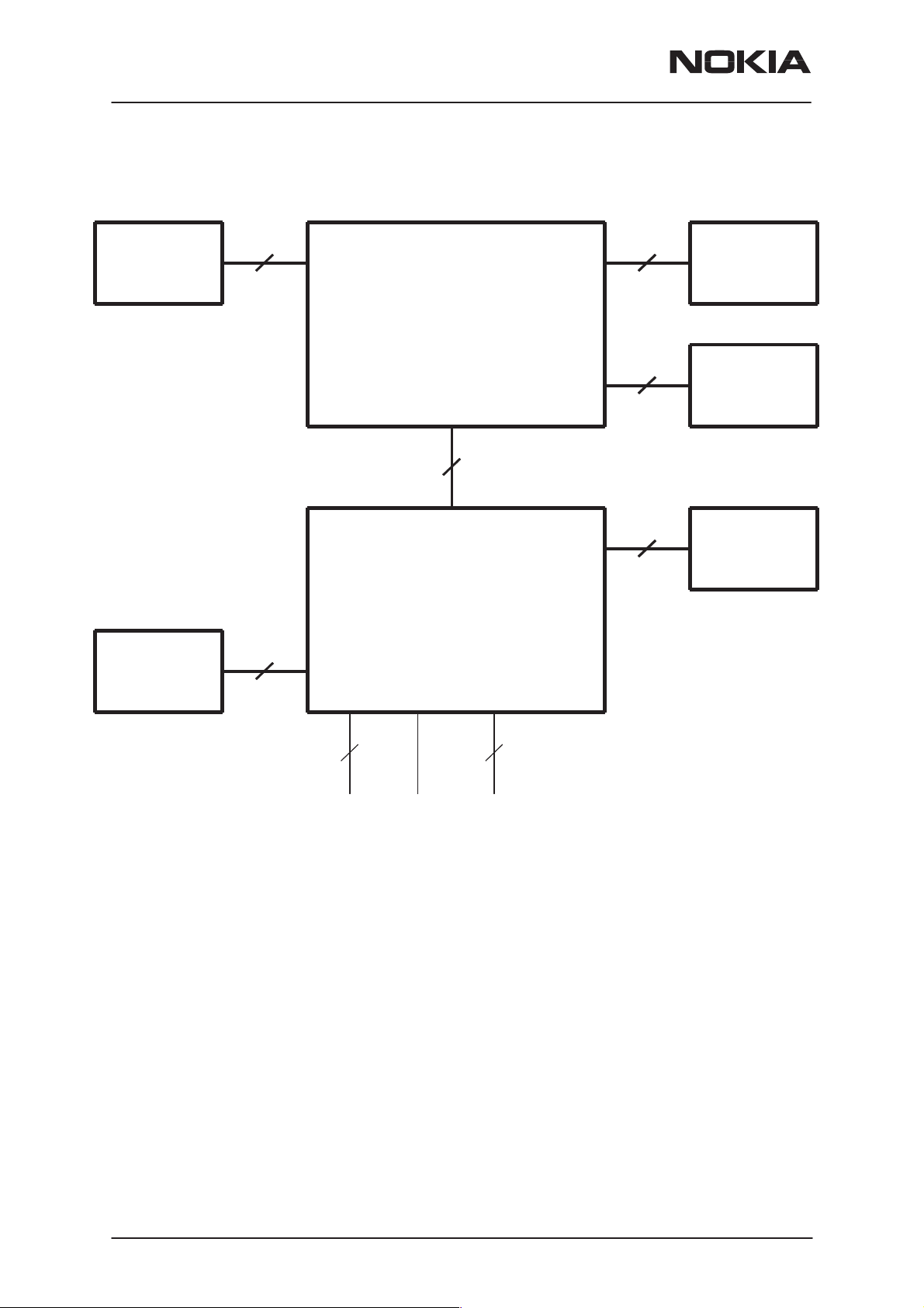
Interconnection Diagram
11 9
Keypad Display
User Interface
Module
Antenna
UE4
2
Earpiece
28
4
Battery
System/RF
Module
1
UF4D
3 + 36+2
Page 6
Nokia Mobile Phones Ltd.
Issue 1 06/1999
Page 7
PAMS Technical Documentation
System Module
Circuit Description
The transceiver electronics consist of the Radio Module, RF + System
blocks, the UI PCB, the display module and audio components. The key-
pad and the display module are connected to the Radio Module with a
connectors. System blocks and RF blocks are interconnected with PCB
wiring. The Transceiver is connected to accessories via a bottom system
connector with charging and accessory control.
The RF block is designed for a handportable phone which operates in the
CDMA 800 system. The purpose of the RF block is to receive and de-
modulate the radio frequency signal from the base station and to transmit
a modulated RF signal to the base station.
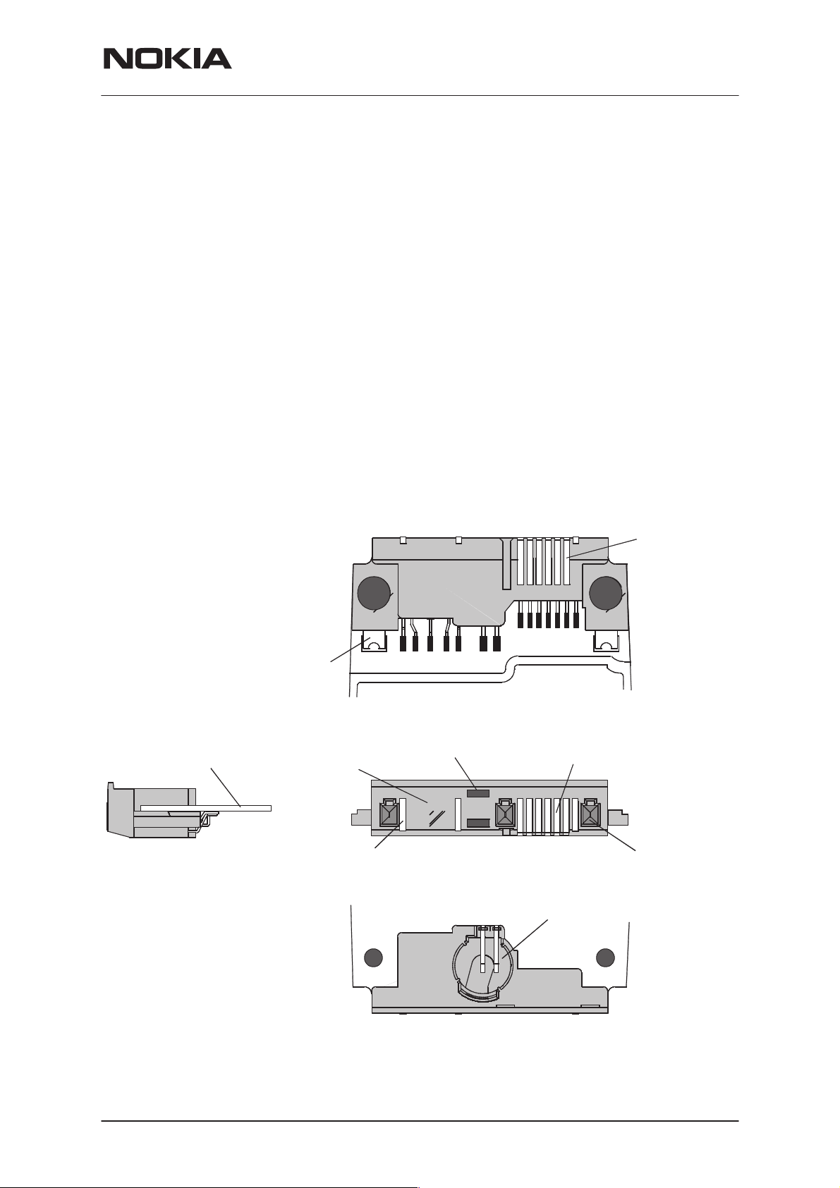
Connectors
NSD–3
System Module
System Connector
B side view
Fixing pads (2 pcs)
Engine PCB
1
DC Jack
Charger pads (3 pcs)
acoustic ports
Microphone
8
7
14
Bottom
connector (6 pads)
Cable locking holes (3 pcs)
Cavity for microphone
IBI connector
(6 pads)
A side view
Note: Intelligent Battery Interface, IBI, is an accessory interface on the
battery side of the phone including the same signals as the bottom con-
nector. The accessory ( e.g. an IBI accessory) can be a battery pack with
Issue 1 06/1999
Nokia Mobile Phones Ltd.
Page 7
Page 8
NSD–3
Á
Á
Á
Á
Á
Á
Á
Á
Á
Á
Á
Á
Á
Á
Á
Á
Á
Á
Á
Á
Á
Á
Á
Á
Á
Á
Á
Á
Á
Á
Á
Á
Á
Á
Á
Á
Á
Á
Á
Á
Á
Á
Á
Á
Á
Á
Á
Á
Á
Á
Á
Á
Á
Á
Á
Á
System Module
special features or an accessory module attached between the phone
and a normal battery pack.
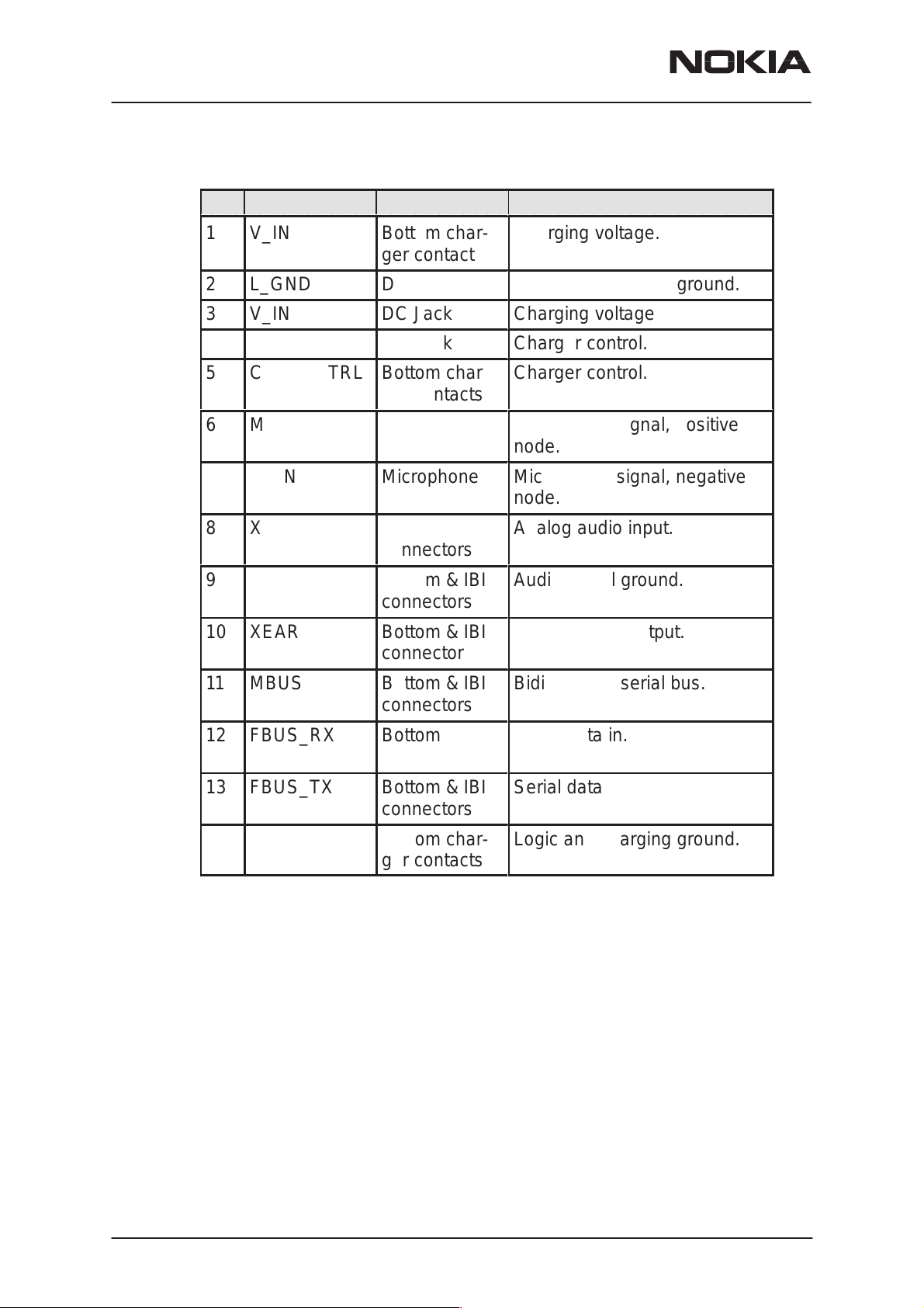
Pin Name Function Description
1
Á
2
3
4
Á
5
Á
Á
6
Á
7
Á
V_IN
ÁÁÁÁ
L_GND
V_IN
CHRG_CTRL
ÁÁÁÁ
CHRG_CTRL
ÁÁÁÁ
ÁÁÁÁ
MICP
ÁÁÁÁ
MICN
ÁÁÁÁ
Bottom charger contacts
БББББ
DC Jack
DC Jack
DC Jack
БББББ
Bottom char-
БББББ
ger contacts
БББББ
Microphone
БББББ
Microphone
БББББ
PAMS Technical Documentation
Charging voltage.
ББББББББББ
Logic and charging ground.
Charging voltage.
Charger control.
ББББББББББ
Charger control.
ББББББББББ
ББББББББББ
Microphone signal, positive
node.
ББББББББББ
Microphone signal, negative
ББББББББББ
node.
8
9
10
11
12
13
14
Á
Á
Á
Á
Á
Á
Á
Á
XMIC
ÁÁÁÁ
SGND
ÁÁÁÁ
XEAR
ÁÁÁÁ
ÁÁÁÁ
MBUS
ÁÁÁÁ
FBUS_RX
ÁÁÁÁ
FBUS_TX
ÁÁÁÁ
L_GND
ÁÁÁÁ
Bottom & IBI
БББББ
connectors
Bottom & IBI
БББББ
connectors
Bottom & IBI
БББББ
connectors
БББББ
Bottom & IBI
connectors
БББББ
Bottom & IBI
БББББ
connectors
Bottom & IBI
БББББ
connectors
Bottom char-
БББББ
ger contacts
Analog audio input.
ББББББББББ
Audio signal ground.
ББББББББББ
Analog audio output.
ББББББББББ
ББББББББББ
Bidirectional serial bus.
ББББББББББ
Serial data in.
ББББББББББ
Serial data out.
ББББББББББ
Logic and charging ground.
ББББББББББ
Page 8
Nokia Mobile Phones Ltd.
Issue 1 06/1999
Page 9
PAMS Technical Documentation
RF–Connector
The RF–connector is needed to utilize the external antenna with Car
Cradle. The RF–connector is located on the back side of the transceiver
on the top section. The connector is plug type connector with special me-
chanical switching.
NSD–3
System Module
Accessory side of connector
Part will be floating in
car holder
Phone side of connector
Issue 1 06/1999
Nokia Mobile Phones Ltd.
Page 9
Page 10
NSD–3
System Module
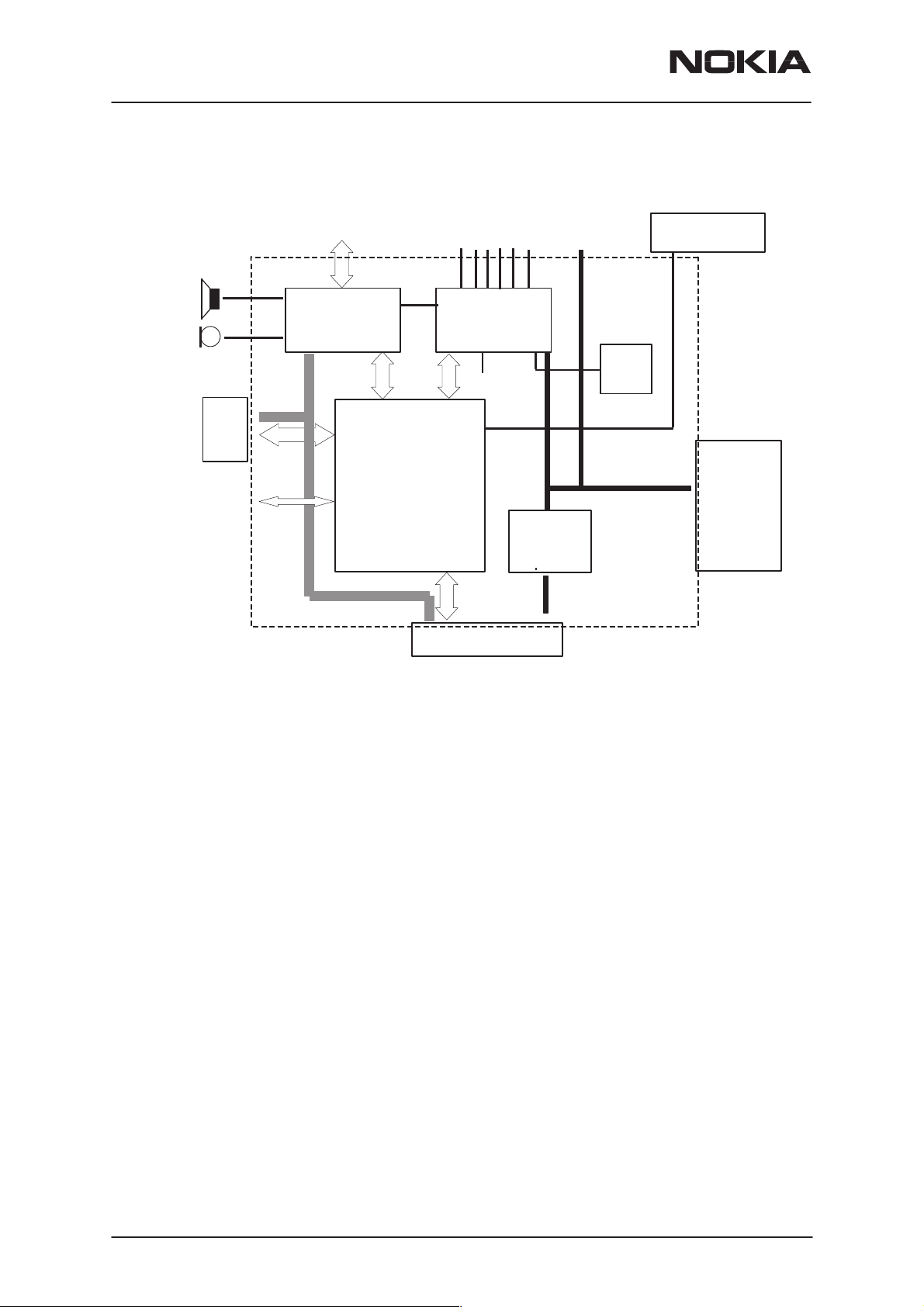
Baseband Module
Block Diagram
PAMS Technical Documentation
UI
TX/RX SIGNALS
BASEBAND
Cafe SUPPLY
Cafe
MEMORIES
AUDIOLINES
MAD
+
RF SUPPLIES
CCONT
BB SUPPLY
SYSCON
PA SUPPL Y
CHARGING
SWITCH
SLEEP CLOCK
32kHz
CLK
VBAT
SYSTEM CLOCK
19.2MHzCLK
BATTERY
Baseband Elements
Baseband refers to all technology elements in the phone design, which do
not include RF functions. The Baseband Module therefore includes audio,
logic control, signal processing, power supply, and user interface func-
tions. Baseband functionality of this product consists of third generation
Digital Core Technology (DCT3) design solutions.
Baseband ASICS Description
MAD4
The MAD4 ASIC contains four main components: DSP, MCU, RAM, and
ROM. This ASIC controls logic functions for the user interface, USART
and PWMs, CAFÉ, Control Timing and Interrupts (CTI), RX Modem, RF
Interface, Accessory Interface, and CDMA functionality.
The DSP controls the RF power and implements the compressor and ex-
pander for AMPS, the vocoders for CDMA and DTMF tone generation.
The MCU performs tasks such as UI control, timers, PUP control, RX Mo-
dem interface, audio control, evaluation of sensor data from CCONT A\D,
and battery charging control.
CAFÉ
Page 10
The CAFÉ ASIC provides CODEC functionality (A/D and D/A conversions
for voice data, microphone and speaker amplification, variable RX and TX
Nokia Mobile Phones Ltd.
Issue 1 06/1999
Page 11

PAMS Technical Documentation
Audio Gain), provides system clock squaring, utilizes PLL for CDMA clock
generation from system clock, and interfaces to the RF section and to
MAD4.
CCONT
The CCONT ASIC provides linear regulated power to most of the phone.
It has a multiplexed A/D converter for temperature sensor digitization, bat-
tery voltage, charger voltage, current consumption, and battery type
detection. An external 32 kHz oscillator circuit is connected to CCONT,
which is used for sleep clock generation. It also has a watchdog circuit
used to power off the phone in the event that MCU receives an interrupt
from power key depression, or an event has caused a process to over run
and MCU does not service the register to prevent the watchdog timer
from timing out.
PENTA
NSD–3
System Module
CHAPS
The PENTA IC chip operates as a low noise, low drop out regulator with 5
independent 2.8–volt outputs used to power on various sections of the RF
module. The PENTA IC has 5 control inputs are controlled by the MAD4
ASIC.
CHAPS operates as an integrated power switch for controlling charger
current. Its features are limited start up current, limited maximum switch
current, transient voltage protection, voltage limit protection, and reverse
voltage protection. It is designed to be used with either a single lithium
cell or three nickel cells battery types.
Issue 1 06/1999
Nokia Mobile Phones Ltd.
Page 11
Page 12

NSD–3
System Module
Memories
SRAM
External SRAM is used by MAD4. Size is 2 Mbit (256k x 8 bit).
FLASH MEMORY
Flash memory contains the main program code for the MCU and default
EEPROM values. Size is 16 Mbit (1M x 16 bit), with layout compatability
for an optional 8 Mbit chip (512k x 16 bit).
EEPROM
An EEPROM is used to store user data and tuning parameters. Size is
256 kbit (32k x 8), with optional 64k x 8 bit. A 2–wire serial interface is
used for communication.
Clocks
System Clock and CDMA Clock
PAMS Technical Documentation
A 19.2 MHz signal is passed to the CAFÉ ASIC from the RF section. The
CAFÉ then generates the 19.2 MHz system clock and the 9.8304 MHz
CDMA clock, which are derived from the RF signal. Both of these clocks
are passed to MAD4.
8kHz Frame Sync Clock
An 8 kHz frame sync is generated in MAD4 and passed to the CAFÉ in
order to synchronize the internal CAFÉ clocks with the equivalent MAD4
clocks. This signal is also used to “frame” the CODEC voice data at 8kHz.
The pulse width of the frame sync will be equal to one period of the 320
kHz clock, which is internal to CAFÉ.
Sleep Clock
Sleep clock is provided by CCONT and produces a 32.768 kHz clock
used by MAD4 when it is in sleep mode. The crystal oscillator in the ex-
ternal CCONT circuitry to CCONT is not automatically started when the
battery is connected, but after power up the oscillator is always running,
even during power off periods. The only exception is when the battery is
removed.
UIF and CCONT Serial Clock (UIF_CCONT_SCLK)
This 960 KHz clock is used to synchronize serial data transmission on the
UIF and CCONT serial data bus UIF_CCONT_SDIO.
Page 12
Nokia Mobile Phones Ltd.
Issue 1 06/1999
Page 13
PAMS Technical Documentation
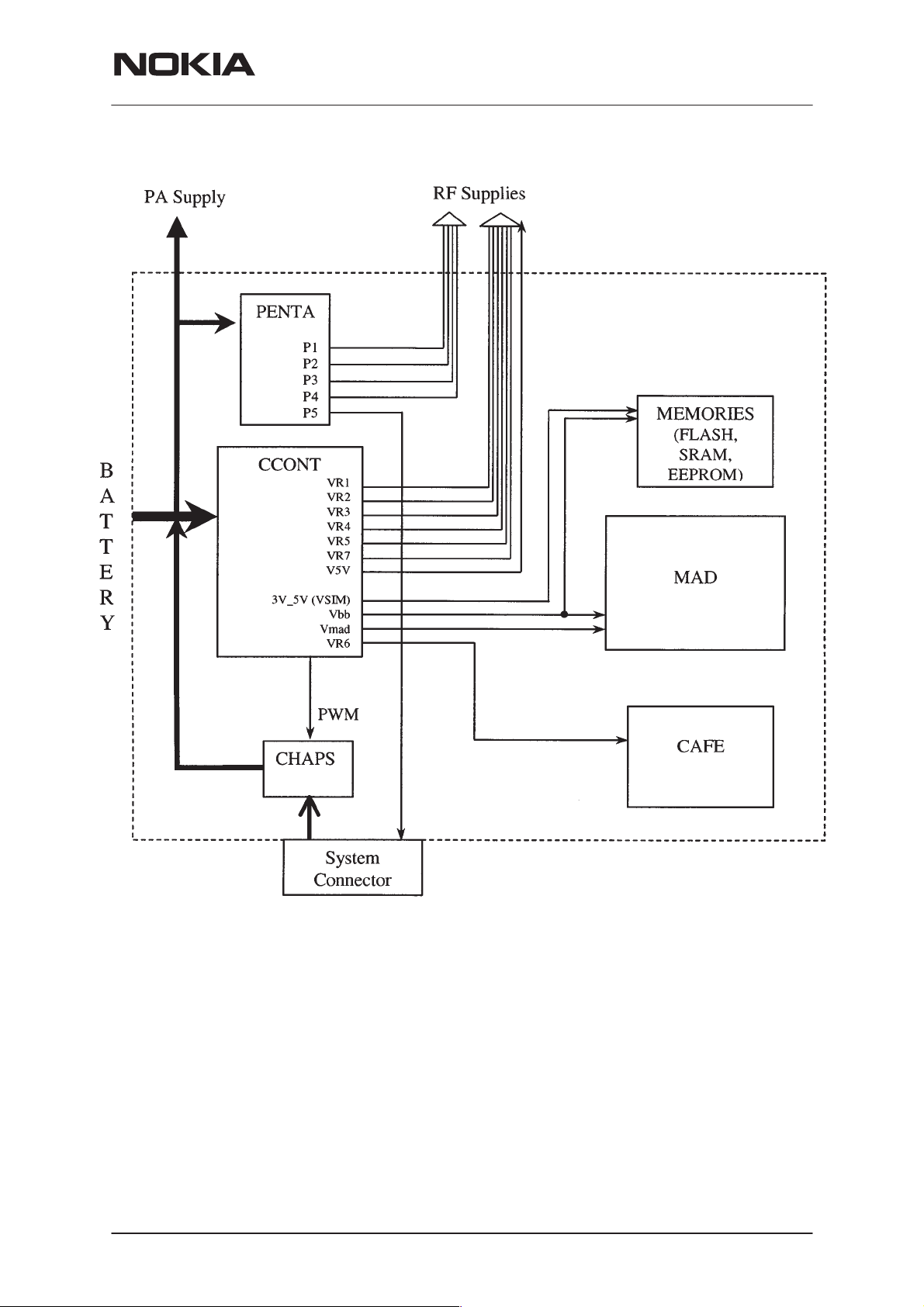
Baseband Power Distribution
NSD–3
System Module
Description
Power management and distribution in the phone is handled by the
CCONT asic. CCONT is a multi function power management IC which
has seven 2.8V linear regulators for the RF–section of the phone. One
2.8V regulator is used to power up the baseband of the phone, and its
output is called Vbb. Additionally, one adjustable regulator is used to pow-
er up certain parts of the baseband. There are also a 5V charge pump,
5V regulator and 3/5V regulator.
The main functions are voltage regulation, power up/down procedures,
reset logic, charging control (PWM) , watchdog, sleep control, ADC and
real time clock.
Issue 1 06/1999
Nokia Mobile Phones Ltd.
Page 13
Page 14

NSD–3
System Module
CCONT Regulators
Battery voltage VBAT is connected to CCONT which regulates all the sup-
ply voltages VBB, VR1–VR7, V2V, VR1_SW, VSIM and V5V. CCONT’s
default startup mode is to turn on VR1, VBB, V2V, VR6 and Vref in pow-
er–up. Vrefs default value is 1.5V, but in in this phone we use 1.25V for
Vref, so one of the first things MAD4 does on power up is to do a write to
CCONT to change Vref to 1.25V.
VBB is used as baseband power supply for all digital parts, and it is on
whenever the phone is powered up. V2V is reserved for a later version of
the MAD4 ASIC which will have a lower core voltage. When the low volt-
age core version of MAD4 is available, V2V will be connected to those
pins on MAD4 which power the core. VSIM is used as programming volt-
age for the Flash memory after the phone is cut out of the panel. This is
necessary if re–flashing is needed after initial flash programming in pro-
duction. V5V is used for RF parts only. VR6 supplies the power for CAFE.
VR1 is used for the VCTCXO supply. VR1_SW is derived from VR1 inside
CCONT, and is actually the same voltage, but can be separately switched
on and off. This VR1_SW is used as an optional external microphone bias
voltage. CLK_EN signal to CCONT controls both the VR1 and VR6 regu-
lators; they can be switched off in sleep modes, during standby.
PAMS Technical Documentation
Charging
CCONT regulators are controlled through a seial data bus from MAD4.
Regulators VR3, 4, 5 and 7 are controllable through external pins; these
pins forming a logical ’OR’ function with the serial commands. If a regula-
tor’s control pin is at logic ’1’, that regulator will turn on. If the pins are not
used for external control they are grounded.
Most of the regulator outputs depend on pin control. In the table the ’State
in reset’ is based on assumption that pin controls are ’0’.
Charging can be performed in any operating mode. The charging algo-
rithm is dependent on the battery technology used. A resistor internal to
the battery pack indicates the battery type. The resistor value corre-
sponds to a specific battery capacity. This capacity value is related to the
battery technology as different capacity values are achieved by using dif-
ferent battery technologies.
The CCONTs A/D converter input measures the battery voltage, tempera-
ture, size and current.
NOTE: Power management circuitry controls the charging current deliv-
ered from the charger to the battery. Charging is controlled with a PWM
input signal from CCONT. The pulse width is controlled by MAD4 and is
sent to CCONT through a serial bus. The battery voltage rise is limited by
turning CHAPS switch off when the battery voltage has reached the de-
sired limits.
Watchdog
Page 14
MAD4 must reset the CCONT watchdog regularly. CCONT watchdog time
can be set through SIO between 0 and 63 seconds at 1 second steps. Af-
Nokia Mobile Phones Ltd.
Issue 1 06/1999
Page 15
PAMS Technical Documentation
ter power–up the default value is 32 seconds. If the watchdog expires,
CCONT will cut off all supply voltages. After total cut–off the phone can
be re–started through any normal power–up procedure. CCONTs watc-
dog functionality may be temporarily disabled by holding CCONTs
PWRONX/WDDISX pin at logic low.
Power Up
There are four ways to power on the phone.
1. Pressing the power button
2. Connecting a charger
3. An IBI interrupt on BTEMP
4. Internal RTC times out.
Each of four methods is described in general in the following sections.
When the battery is connected to phone, nothing will happen until the
power–up procedure is initiated, for instance by pressing the power–but-
ton or by connecting a charger. After that the 32kHz crystal oscillator of
CCONT is started (can take up to 1 sec), and the default regulators are
powered up.
NSD–3
System Module
If a power down is done and the battery remains connected, the 32 kHz
crystal oscillator keeps running in the CCONT.
VCTCXO
CAFE
FLASH
RF
VCHAR
CHAPS
VBAT
PWM
BATTERY
CCONT
VR1_SW
MAD
VR1
VR6
VBB
SIO
VSIM
V5V
Vref
Power distribution diagram
VR1–VR7
Issue 1 06/1999
Nokia Mobile Phones Ltd.
Page 15
Page 16

NSD–3
System Module
Pressing power key
PWRONX
VR1, VBB, VR6
CLK_EN
VCTCXO
CAFE CLK
PURX
SLCLK
PAMS Technical Documentation
t1
t2
t3
t1 < 1 ms
t2 1 – 6 ms, VCXO settled
t3 62 ms, PURX delay generated by CCONT
After PWR–key has been pushed, CCONT gives PURX reset to MAD4
and turns on VR1, VBB and VR6 regulators (if battery voltage has ex-
ceeded 3.0 V). VR1 supplies VCTCXO, VBB supplies MAD, and VR6 sup-
plies digital parts of CAFE. After the initial delay, t2, VCTCXO starts to
give a proper 19.2MHz clock to CAFE, which further divides it to 9.83MHz
for MAD4. CAFE will output the 9.83MHz clock only after the PURX reset
has been removed. After delay, t3, CCONT releases PURX and MAD4
can take control of the operation of the phone.
After MAD4s reset is released MCU–SW detects that the PWR–key is still
pushed and shows the user that the phone is powering up by turning on
the LCD and the lights. MCU–SW then powers up the RF receiver part.
Page 16
V5V–regulator (for RF) default value is off in power–up, and can be con-
trolled on via serial bus when needed.
Nokia Mobile Phones Ltd.
Issue 1 06/1999
Page 17

PAMS Technical Documentation
Power up when charger connected
Normal battery voltage
VCHAR
VR1, VBB, VR6
CLK_EN
VCTCXO
9.83 MHz CLK
PURX
SLCLK
NSD–3
System Module
CCONTINT
Power up, charger connected, VBAT > 3.0 V
The power up procedure is similar to the process described in the pre-
vious chapter with the exception that the rising edge of VCHAR triggers
the power up in CCONT.
CCONT sets output CCONT_INT, MAD4 detects the interrupt and reads
CCONT status register to find the reason for the interrupt (charger in this
case). After reading the A/D register to determine that the charger voltage
is correct MAD should initiate charging activities. The phone will remain in
the so called ”acting dead” state which means that only the battery bars
are displayed on the LCD. The user perceives that the phone is off. If the
power on button is pushed the LCD display will come on and startup will
be the same as normal power on.
CCONT_INT is generated both when the charger is connected, and when
the charger is disconnected.
t1
t2
t3
Issue 1 06/1999
Nokia Mobile Phones Ltd.
Page 17
Page 18

NSD–3
System Module
Empty battery
VBAT > 3.0 V
VCHAR
VR1, VBB, VR6
CLK_EN
VCTCXO
9.83MHz
PURX
SLCLK
PAMS Technical Documentation
CCONT_INT
Power up, charger connected, VBAT < 3.0 V
Before battery voltage voltage rises over 3.0 V CHAPS gives an initial
charge (with limited current) to the battery. After battery voltage reaches
3.0V the power up procedure is as described in the previous section.
If a power down is done and the battery remains connected, the 32 kHz
crystal oscillator keeps running in the CCONT. When a power–up is initi-
ated again, the complete power–up sequence is described in the figure
below. This time the power–up sequence is faster because the oscillator
is already running.
Charging – CHAPS
CHAPS comprises the hardware for charging the battery and protecting
the phone from over–voltage in charger connector.
t1
t2
t3
Page 18
The main functions are:
–transient, over–voltage and reverse charger voltage protection
–limited start–up charge current for a totally empty battery
–voltage limit when battery removed
–with SW protection protection against too high charging current
CHAPS is basically a PWM (Pulse Width Modulation) controlled switch
which connects the charger to VBAT. MAD4 controlls CHAPS by writing
PWM values to CCONTs PWM register over a serial bus. CCONT then
Nokia Mobile Phones Ltd.
Issue 1 06/1999
Page 19

PAMS Technical Documentation
outputs a PWM which is used by CHAPS to control the switch. In the case
of an external fast charger, the PWM is available at the system connector
to control the charger. In the case of a dead battery, shorted battery, or if
the battery is below 3.0V, CHAPS supplies a controlled leakage current of
about 180mA through the switch to attempt to bring the battery voltage
up.
NSD–3
System Module
Pin
num-
ber
1, 16 VCH Charger voltage input
5 RSENSE High current output, connected to current sense
12 VBAT Battery voltage (connected to voltage sense part of CHAPS)
10 VBACK Backup battery charging voltage output
9 LIM Output voltage limit select input
7 PWM Charging switch control input
8 CTIM External capacitor for soft switching
2, 3, 4,
6, 11,
13, 14,
15
Name Description
resistor of phone
GND Ground
CHAPS
BATTERY
Vin
MAD
System
Connector
To
charger
PWMOUT
Charging Control
CCONT
serial control
V_charge
2–wire charging
With 2–wire charging the charger provides constant output current, and
the charging is controlled by PWMOUT signal from CCONT to CHAPS.
PWMOUT signal frequency is selected to be 1 Hz, and the charging
switch in CHAPS is pulsed on and off at this frequency. The final charging
current to the battery is controlled by adjusting the PWMOUT signal pulse
width.
Both the PWMOUT frequency selection and pulse width control are made
by the MCU which writes these values to CCONT.
Issue 1 06/1999
Nokia Mobile Phones Ltd.
Page 19
Page 20

NSD–3
System Module
The 2–wire charger is part number ACP–7, has full–wave rectified output,
defined output voltage and impedance. Typical output current into empty
battery is about 350 mA at nominal mains voltage.
3–wire charging
With 3–wire charging the charger provides adjustable output current, and
the charging is controlled by PWMOUT signal from CCONT to Charger,
with the bottom connector signal. PWMOUT signal frequency is selected
to be 32 Hz, and the charger output voltage is controlled by adjusting the
PWMOUT signal pulse width. The charger switch in CHAPS is constantly
on in this case.
The 3–wire charger is part number ACP–9, a switchmode power supply
(SMPS) adapter using 3–wire charging structure (controlled constant volt-
age). Typical output into an empty battery is about 850mA at nominal
mains voltage.
Battery disconnected when charger is connected
From hardware point of view the phone could otherwise continue func-
tioning normally, but if the charger voltage is higher than the maximum
allowed battery voltage, this can damage the RF parts. Therefore, output
overvoltage protection is needed in case the battery is removed when a
charger is connected, or if a charger is connected before the battery to
the phone. With a charger connected, if VBAT exceeds preset limits in
CHAPS, the switch turns OFF immediately (soft switching bypassed).
There are two voltage limits, VLIM1 and VLIM2. VLIM input = ’0’ selects
VLIM1, VLIM input = ’1’ selects VLIM2.
PAMS Technical Documentation
Parameter Symbol Min Typ Max Unit
Output voltage cutoff limit (during
transmission or Li–battery)
Output voltage cutoff limit (no
transmission or Ni–battery)
VLIM1 4.4 4.6 4.8 V
VLIM2 4.8 5.0 5.2 V
When the switch turns off due to an overvoltage condition, it stays off until
the input voltage falls below the specified limit (VCH<VBAT). Phone soft-
ware will stop the charging as fast as it detects that there is no battery
present.
Page 20
Nokia Mobile Phones Ltd.
Issue 1 06/1999
Page 21

PAMS Technical Documentation
VBAT
VLIM
4V
PWM
”1”
”0”
SWITCH
ON
NSD–3
System Module
t
t
1.1Battery removed, (standard) charger connected, VBAT rises (follows charger voltage)
2. VBAT exceeds limit VLIM(X), switch is turned immediately OFF
3.3VBAT falls (because no battery) , also VCH<VBA T (standard chargers full–rectified
output). When VCH > VBAT and VBAT < VLIM(X) –> switch turned on again (also PWM
is still HIGH) and VBAT exceeds VLIM(X).
4. Software sets PWM = LOW –> CHAPS does not enter PWM mode
Output overvoltage protection when battery removed ( in principle )
Power Down
Pressing power key
When the user wishes to turn the phone off and presses the power key,
MAD (MCU SW) detects that PWR–key is pressed for a long enough
time. After that the lights and LCD are turned off. MCU stops all the activities it was doing (e.g. ends a call), sends power off command to CCONT
by writing a ’zero’ amount of time to the watchdog register, and goes to
idle–task. After the delay CCONT cuts all the supply voltages from the
phone. Only the 32 kHz sleep clock remains running.
OFF
2
4
t
Note that the phone doesn’t go to power off (from HW point of view) when
the charger is connected and PWR–key is pushed. The user perceives
that the phone is off, but in fact the phone is just acting as if it is off (this
state is usually called ”acting dead”).
Battery charge low
As a battery discharges, energy management software keeps a constant
watch on the voltage and displays an appropriate amount of battery bars.
Issue 1 06/1999
Nokia Mobile Phones Ltd.
Page 21
Page 22

NSD–3
System Module
When the battery discharges to a critical level the software notifies the
user by beeping. If left on, the software will power off the phone at a
VBAT of
If the SW fails to power down the phone, hardware will take over and
CCONT will do a reset and power down the phone when the battery voltage drops below 2.8 V.
Watchdog expires
If the SW fails to update the watchdog, the watchdog will eventually expire and CCONT cuts all the supply voltages to the phone. On startup, the
initial value set in CCONT’s watchdog timer register is 32.5 seconds. The
watchdog is programmable from 0 to 63 seconds.
Disconnected battery
When battery is disconnected, immediate and totally uncontrolled power–
down happens. Therefore a power off procedure in this case can not be
described. One possible risk is that if the MCU is writing something to the
EEPROM exactly at the same moment, the memory contents may be corrupted.
TBD
PAMS Technical Documentation
V.
RF to Baseband Interface
The RF to Baseband interface consists of MAD4 and CAFÉ communicating with various parts of the RF module. The MAD4 ASIC produces the
Pulse Duration Modulators (PDMs) which allow analog voltages to be
used for RF control. It also controls the VCTCXO enable, as well as band
and mode selects. MAD also controls the RF supply voltages through
CCONT. The CAFÉ ASIC performs the A/D and D/A conversions for
CDMA and AMPS RX and TX paths. CAFÉ also receives the VCTCXO
19.2 MHz signal and provides MAD4 with the 19.2 MHz system clock.
Page 22
Nokia Mobile Phones Ltd.
Issue 1 06/1999
Page 23

PAMS Technical Documentation
Audio control
Audio Controls and Processing
The audio control is handled by the MAD4 MCU. Speech coding functions
are performed in MAD4 DSP. In transmission mode, the speech code is
then sent to the CAFÉ ASIC for D/A conversion. In receiver mode, PCM
coded blocks are read from the CAFE ASIC Both audio and RF CODECs
reside in CAFÉ.
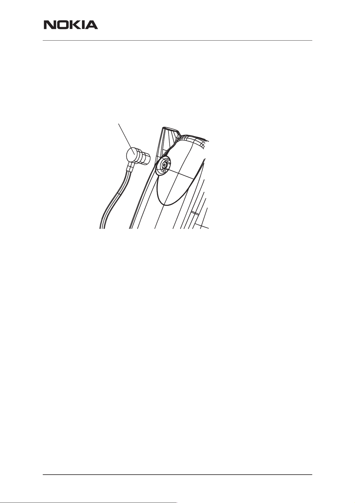
Earpiece
The internal earpiece is connected to the UI board by means of mounting
springs for automated assembly. The 32–ohm impedance, dynamic type
earpiece is connected to the differential output of the CAFÉ ASIC.
Microphone
The internal microphone is connected to the bottom connector by means
of mounting springs. The microphone bias is provided by the CAFÉ ASIC.
Audio Accessory Interface
NSD–3
System Module
External audio is interfaced to the phone through the system connector.
XEAR, XMIC, and SGND are the phone’s external audio signal pins used
for communication during a hands free accessory call.
Issue 1 06/1999
Nokia Mobile Phones Ltd.
Page 23
Page 24

NSD–3
System Module
Digital control
MAD4
The baseband functions are controlled by the MAD asic, which consists of
a MCU, a system ASIC and a DSP. The CDMA specific asic is named as
MAD4.
MCU
For general purpose processing applications.
DSP
The DSP is in charge of the channel and speech coding. The Main interfaces are to the MCU, and via System Logic to CAFE and RF.
System Logic
Peripheral interface:
S MCU Parallel I/O, UART, and PWM control (PUP)
PAMS Technical Documentation
Serial Accessory Interface (FBUS):
S Autobauding support (AccIf)
S Interface to external memories
S Address lines and chip select decoding (BUSC)
S RF Interface and Control (RFIfCtrl)
S Clocking, timing and interrupts (CTI)
S Sleep Control (SleepBlk)
S CAFE Control (CAFECtrl)
User Interface Control (UserIf)
Reset Generator (RstGen)
Clock Generator (ClkGen)
Test Interface (TestIf)
MAD Interfaces
UI and CCONT Serial interface
MAD4s serial interface is used to control the Serial LCD on the User Interface board, and to provide access to CCONTs registers. The DataSelX
and DataClk are generated by MAD4 during both transmit and receive
cycles. Each device has its own chip select signal and must hold its data
pin in a high impedance state if its chip select is not active. Data must be
valid on the rising edge of DataClk during both transmit and receive.
Page 24
CAFE Interface
The MAD4 ASIC supplies an interface to the CAFE ASIC. This interface
consists of parallel transmit and receive busses for CDMA and AMPS
data, and a serial interface for Codec control and data.
E Nokia Mobile Phones Ltd.
Issue 1 06/1999
Page 25

PAMS Technical Documentation
FBUS
FBUS (Fast Bus) is a fast serial interface between the DSP and data accessories or the DSP and multipath analyzer. This interface is a full–duplex, asynchronous, two–line bus.
mdMCUSDIO (Serial Clk)
NSD–3
System Module
Tsds
Tsdh
accFBusRXD (Serial Data)
Data 0 Data 1
...
Data 7
USART Synchronous Mode Receive (Flashing Mode)
MBUS
MBUS is the MCUs serial interface which is used for FLASH downloading
(not program code), testing, and communication with external devices.
Supported baud rates are 9.6, 19.2, 38.4 and 57.6 kbit/s.
JTAG Interface
The JTAG interface is used for MAD4 ASIC emulation. This interface provides for coemulation of the DSP and MCU.
TRUST Interface
TRUST (Trace Utility for Software Testing) is a hardware module used to
capture tracing data from a phone during testing. It serves as a buffer
memory, storing data from the address and data buses of the phone MCU
until read by a PC. A time label is attached to each data word. The unit
also includes a buffer for commands from the PC to the phone.
Signal Definitions
SIGNAL NAME DESCRIPTION From/To Signal Charac-
teristics
Busses, Strobes,
and Clocks
ADD(20:0) 21–Bit Memory Address Bus MAD4 to FLASH
DATA(15:0)
RXD(11:0) Receive Data CAFE to MAD4 0 to 2.8V Digital
Includes parallel and serial
busses as well as data clocks,
and chip selects
and SRAM
16–Bit Memory Data Bus MAD4 to FLASH
and SRAM
0 to 2.8V Digital
0 to 2.8V Digital
Notes
TXD(7:0) Transmit Data MAD4 to CAFE 0 to 2.8V Digital
EEPROMSCLK SCLK to serial EEPROM MAD4 to EE-
PROM
EEPROMSDA Serial data line for serial EE-
PROM.
UIF_CCONT_SCLK Clock for UI and CCONT serial
interface
UIF_CCONT_SDIO User Interface and CCONT Seri-
al Data
Issue 1 06/1999
Nokia Mobile Phones Ltd.
MAD4 to EE-
PROM
MAD4 to
CCONT and UI
connector
MAD4 to
CCONT and UI
connector
0 to 2.8V Digital
0 to 2.8V Digital
(Pullup)
0 to 2.8V Digital
0 to 2.8V Digital
Page 25
Page 26

NSD–3
System Module
PAMS Technical Documentation
From/ToDESCRIPTIONSIGNAL NAME
teristics
CCONTCSX CCONT Chip Select MAD4 to
CCONT
LCDCS LCD Chip Select MAD4 to UI con-
nector
MEM(3) Memory Read Strobe MAD4 to FLASH
and SRAM
MEM(2) Memory Write Strobe MAD4 to FLASH
and SRAM
MEM(1) RAM Chip Select MAD4 to SRAM 0 to 2.8V Digital
MEM(0) FLASH chip enable MAD4 to FLASH 0 to 2.8V Digital
MBUS MCU serial bus for external com-
munication
FBUS_TX DSP Accessory UART Data Out-
put
FBUS_RX DSP Accessory UART Data In-
put
ADATA AMPS Data Input to RxModem
(MAD4)
CAFESIO(2) CAFE I/F Frame Sync MAD4 to CAFE 0 to 2.8V Digital
MAD4 to System
connector
MAD4 to System
connector
System connec-
tor to MAD4
CAFE to MAD4 0 to 2.8V Digital
0 to 2.8V Digital
0 to 2.8V Digital
0 to 2.8V Digital
0 to 2.8V Digital
0 to 2.8V Digital
0 to 2.8V Digital
0 to 2.8V Digital
NotesSignal Charac-
CAFESIO(1) CAFE I/F Serial Data from CAFE CAFE to MAD4 0 to 2.8V Digital
CAFESIO(0) CAFE I/F Serial Data to CAFE MAD4 to CAFE 0 to 2.8V Digital
CLK9M20 19.2MHz System Clock CAFE to MAD4 0 to 2.8V Digital
CLK9M83 9.8304MHz CDMA Clock CAFE to MAD4 0 to 2.8V Digital
SLEEPCLK 32.768kHz Sleep Clock CCONT to
MAD4
RF Interface Control Signals
CAFE_TX_GATE Transmitter Gating Signal MAD4 to RF 0 to 2.8V Digital
TIF_EN TIF chip enable MAD4 to RF 0 to 2.8V Digital
SYN_ACQ&SYN_P
WR_DN
SYN_LK1 MAD4 to RF 0 to 2.8V Digital
RIF_EN MAD4 to RF 0 to 2.8V Digital
TX_LIM Indicates TX Power Greater than
TXI_REF
SYN_CLK R/F I/F Serial Clock MAD4 to RF 0 to 2.8V Digital
SYN_DAT R/F I/F Serial Data MAD4 to RF 0 to 2.8V Digital
MAD4 to RF 0 to 2.8V Digital
RF to MAD4
0 to 2.8V Digital Oscillator still
running when
phone is powered down.
SYN_LE1 R/F I/F Serial Latch Enable #1 MAD4 to RF 0 to 2.8V Digital
CEL_MODE R/F I/F Serial Latch Enable #2 MAD4 to RF 0 to 2.8V Digital
BAND_SEL RF Frequency Band Select (PCS
or Cellular)
MODE_SEL RF Mode Select (CDMA or
AMPS)
Page 26
Nokia Mobile Phones Ltd.
MAD4 to RF 0 to 2.8V Digital
MAD4 to RF 0 to 2.8V Digital
Issue 1 06/1999
Page 27

PAMS Technical Documentation
NSD–3
System Module
From/ToDESCRIPTIONSIGNAL NAME
teristics
AFC AFC PDM MAD4 to RF 0 to 2.8V contin-
uously variable
RX_IF_AGC Receive IF AGC PDM MAD4 to RF 0 to 2.8V contin-
uously variable
TX_IF_AGC Transmit IF AGC PDM MAD4 to RF 0 to 2.8V contin-
uously variable
TX_RF_AGC Transmit RF AGC PDM MAD4 to RF 0 to 2.8V contin-
uously variable
TX_VCO_CAL PENTA Regulator control (P5) MAD4 to RF 0 to 2.8V Not used as a
TX_LIM_ADJ General Purpose PDM2 MAD4 to RF 0 to 2.8V contin-
uously variable
FIL T_SEL General Purpose PDM3 MAD4 to RF 0 to 2.8V Digital Not used as a
BOOST General Purpose PDM4 MAD4 to RF 0 to 2.8V contin-
uously variable
RX_GS RF Receive Gain Switch function MAD4 to RF 0 to 2.8V Digital
RF_TX_GATE_P Transmitter Gating Signal (PCS
Mode)
RF_TX_GATE_C Transmitter Gating Signal (Cellu-
lar Mode)
CLK_EN VCTCXO Enable (to CCont
”SLEEPX” input)
MAD4 to RF 0 to 2.8V Digital
MAD4 to RF 0 to 2.8V Digital
MAD4 to
CCONT
0 to 2.8V Digital Signal to
NotesSignal Charac-
PDM
PDM
CCONT which
controls regulators to RF.
VLIM Used to select the max battery
voltage for the charging circuit in
CHAPS (VLIM1 or VLIM2).
Peripherals, Accessory Inter-
face, and A/Ds
BUZZER Buzzer PWM Output MAd4 to UI con-
VIBRA PWM output for vibra motor MAD4 to on
HOOKINT Hook Interrupt CAFE to MAD4 0 to 2.8V Digital
EAD_HEADINT Headset Interrupt (CCONT per-
forms A/D on this signal).
tp4 DBUS data line test point MAD4 0 to 2.8V Digital
RS232_PWR Control for switching power onto
SGND while using a data cable
accessory.
BSI Intelligent Battery Interface. A/D
input to CCONT.
MAD4 to CHAPS 0 to 2.8V Digital
0 to 2.8V Digital
nector
0 to 2.8V Digital
board VIBRA cir-
cuit, and to bat-
tery connector
via BTEMP line
CAFE to MAD4
and CCONT
N306 (regulator)
to System con-
nector
Battery connec-
tor to CCONT
0 to 2.8V Digital Controlled by
DC voltage level
that varies with
different battery
types.
MAD4
Voltage divider
A/D input to
CCONT
Issue 1 06/1999
Nokia Mobile Phones Ltd.
Page 27
Page 28

NSD–3
System Module
PAMS Technical Documentation
BTEMP A/D input to CCONT. Used for
battery temperature detection
and battery VIBRA control.
PA_TEMP A/D input to CCONT. Used for
RF power amp temperature
detection.
RSSI A/D input to CCONT. Receive
signal strength indicator for
AMPS mode.
V_IN Power in from charger
Ground reference for charger
L_GND
(Separated from GND through
an inductor).
Regulator Control Signals
From/ToDESCRIPTIONSIGNAL NAME
teristics
Battery Connec-
tor to CCONT
RF to CCONT DC voltage level
RF to CCONT DC voltage level
System connec-
tor to CHAPS
System connec-
tor to GND via
inductor
DC voltage level
which changes
with battery temperature.
which changes
with PA temperature.
which changes
with received
signal strength.
ACP–9 DC
ACP–7 Rectified
AC
0V
NotesSignal Charac-
Thermistor voltage divider A/D
input to CCONT
Thermistor voltage divider A/D
input to CCONT
Voltage will
change with
charge control
PWM.
VREGP1 Controls voltage regulator P1
(PENTA).
VREGP2 Used to control voltage regulator
P2 (PENTA). This signal is also
the MSB (bit–21) of the Memory
Address Bus but is not used as
an address bit.
VREGP3 Controls voltage regulator P3
(PENTA).
VREGP4 Controls voltage regulator P4
(PENTA).
CCONT_INT CCONT interrupt to MAD4 CCONT to
User Interface Board Peripher-
als
FLIP Flip interrupt (detects status of
hinge) on variants with flip fea-
ture.
BACKLIGHT Controls illumination on UI board. MAD4 to UI con-
CALL_LED Controls the call LED on UI
board.
MAD4 to
CCONT
MAD4 to
CCONT
MAD4 to
CCONT
MAD4 to
CCONT
MAD4
UI connector to
MAD4
nector
MAD4 to UI con-
nector
0 to 2.8V Digital
0 to 2.8V Digital
0 to 2.8V Digital
0 to 2.8V Digital
0 to 2.8V Digital
0 to 2.8V Digital
0 to 2.8V Digital
0 to 2.8V Digital
LCD_RESETX Resets the LCD on the UI board. MAD4 to UI con-
nector
COL(4:0) Keyboard Columns on UI board. MAD4 to UI con-
nector
UIF(5:0) Keyboard Rows and LCD I/F MAD4 to UI con-
nector
Page 28
Nokia Mobile Phones Ltd.
0 to 2.8V Digital
0 to 2.8V Digital
0 to 2.8V Digital
Issue 1 06/1999
Page 29

PAMS Technical Documentation
NSD–3
System Module
From/ToDESCRIPTIONSIGNAL NAME
teristics
PWRONX Power button signal UI connector to
MAD4
Resets
PURX Power Up Reset CCONT to
MAD4
RESETX System Reset MAD4 to CAFE 0 to 2.8V Digital
CAFE RF/IF
IQSEL IQ Select control line for select-
ing I or Q data
RXIQ(3:0) CDMA Receive I and Q data RF to CAFE Differential I and
TXIQ(3:0) CDMA Transmit I and Q data CAFE to RF Differential I and
LIM_P non–inverting AMPS receive
modulated signal
LIM_N Inverting AMPS receive modu-
lated signal
CLK19M2RF 19.2MHz sinusiod from RF RF to CAFE sinusoid
MAD4 to CAFE 0 to 2.8V Digital
RF to CAFE analog
RF to CAFE analog
0 to 2.8V Digital
0 to 2.8V Digital
Differential Q
Differential Q
NotesSignal Charac-
AMPSMOD AMPS audio signal (after
DSPand D/A) to be transmitted.
Test & Emulation
JTAG1_TRST JT AG Reset MAD4 0 to 2.8V Digital
JTAG2_TDI JTAG Scan Input MAD4 0 to 2.8V Digital
JTAG3_TDO JTAG Scan Output MAD4 0 to 2.8V Digital
JTAG4_TCK JTAG Clock & ATPG Scan Clock MAD4 0 to 2.8V Digital
JTAG5_PD JTAG Mode Select & ATPG
Scan Enable
JTAG0 DSP/MCU Emulation (NOT
USED)
JTAG6 DSP/MCU Emulation (NOT
USED)
DSP External Flag
(NOTE: This pin has a dual function as General Purpose I/O
”P0GPIO(6)”. DSPXF is default
function.)
CHRG_CTRL_A DSP Serial Port Input Clock (for
multipath analyzer)
CAFE to RF analog (voice)
MAD4 0 to 2.8V Digital
MAD4 0 to 2.8V Digital
MAD4 0 to 2.8V Digital
MAD4 0 to 2.8V Digital
MAD4 0 to 2.8V Digital
TP5 DSP Serial Port Frame Sync(for
WDDIS Watchdog Disable Test Connector
CCONT Outputs
Issue 1 06/1999
multipath analyzer)
Nokia Mobile Phones Ltd.
MAD4 0 to 2.8V Digital
0 to 2.8V Digital Used in factory
to CCONT
while still in panel
Page 29
Page 30

NSD–3
System Module
PAMS Technical Documentation
From/ToDESCRIPTIONSIGNAL NAME
teristics
VBB LEAD power pins (DSP) CCONT to
MAD4 and me-
mories as the UI
connector
VR1_SW Power for microphone bias CCONT to V201
(CAFE)
VR1 Provides RF power to RF 2.8V regulator
VR2 Provides RF power to RF 2.8V regulator
VR3 Provides RF power to RF 2.8V regulator
VR4 Provides RF power to RF 2.8V regulator
VR5 Provides RF power to RF 2.8V regulator
VR6 Provides power to CAFE to RF 2.8V regulator
VR7 Provides RF power to RF 2.8V regulator
VR7A provides RF power to RF 2.8V regulator regulator exter-
VREF
VMAD
+5V_POWER Provides 5V power to RF to RF 4.7 to 5.2V Charge pump
Used by CAFE as an A/D voltage reference
Provides power to the MAD4
core. Will be used only with the
ROM3 version of MAD4.
to CAFE 1.244V reference
CCONT to
MAD4
2.8V regulator
2.8V regulator
1.8V regulator
NotesSignal Charac-
nal to CCONT
Programmable to
different voltages
3V_5V
CHRG_CTRL
Audio Signals
EARN Inverting part of the audio differ-
EARP Non–inverting part of the audio
XEAR Single ended audio signal to bot-
MICP Non–inverting part of the audio
Provides 3V to flash (Vpp) for
programming
Charge control PWM signal for
accessories
ential signal to the earpiece.
differential signal to the earpiece.
tom connector.
differential signal to the internal
microphone.
CCONT to
FLASH
System connec-
tor to CHAPS.
Can also be driv-
en by CCONT
CAFE to UI con-
nector
CAFE to UI con-
nector
CAFE to System
connector
System connec-
tor (mic) to
CAFE
2.7 to 3.3V used at 3V
0 to 2.8V Digital
1.8Vp–p max combined differential output
from earn and
earp is 3.6Vp–p
max
1.8Vp–p max combined differential output
from earn and
earp is 3.6Vp–p
max
1.8Vp–p max single ended
Can be used up
to 1Vp–p
combined differential input from
MICP and MICN
is 2Vp–p max
Page 30
Nokia Mobile Phones Ltd.
Issue 1 06/1999
Page 31

PAMS Technical Documentation
NSD–3
System Module
MICN Inverting part of the audio differ-
ential signal to the internal microphone.
XMIC
Single ended external audio input from the bottom connector.
SGND Return path for accessory audio,
and power for data cable.
CAFE Submodule
CDMA RX
The MAD/CAFE RX Interface consists of a 12–bit data bus RXD(11:0)
output from the CAFE ASIC to the MAD ASIC. In CDMA mode the data
transfer rate is 9.8304MHz. The RX data is clocked out of the CAFE ASIC
on the falling edge of the 9.8304MHz clock, and clocked into the MAD
ASIC on the rising edge. For CDMA mode the 4–bit RXI data is supplied
on bits RXD(5:2) and the 4–bit RXQ data is supplied on bits RXD(11:8).
Bits (7), (6), (1) and (0) are not used in CDMA mode.
From/ToDESCRIPTIONSIGNAL NAME
System connec-
tor (mic) to
CAFE
System connec-
tor to
System connector to CAFE and
N306
teristics
Can be used up
to 1Vp–p
Can be used up
to 1Vp–p
nearly 0V. Has
some AC components.
NotesSignal Charac-
combined differential input from
MICP and MICN
is 2Vp–p max
Capacitively
coupled input to
CAFE. Resistive
pulldown
TXGATE
TXD(7:0)
CLK9M8O
IQSEL
CLK9M8O
RXD(11:0)
t
DRXD
LAST VALUE READ DATA FROM CAFE LAST VALUE
t
DRXD
Digital Mode RX Data Bus Timing
CDMA TX
CDMA TX data is transferred from MAD4 to CAFE by using an 8–bit multiplexed parallel data bus TXD(7:0). The data is clocked out of MAD on
the rising edge of the clock and clocked into the CAFE on the falling edge
of the clock. The bus data rate is 9.8304 MHz.
t
DON’T
CARE
t
TXGS
TXGON
VALID DATA
FROM MAD
t
DSU
t
IQSU
IQ
VALID DATA
FROM MAD
t
DH
VALID DATA
FROM MAD
t
IQH
t
TXGOFF
DATA FROM
MAD
DON’T
CARE
t
TXGH
Digital Mode TX Data Bus Timing
Issue 1 06/1999
Nokia Mobile Phones Ltd.
Page 31
Page 32

NSD–3
System Module
AMPS RX
AMPS receive data from the RF section is differential, through pin 23 and
24 of the CAFE ASIC. RX data is transferred at 40 kHz through a 12–bit
data bus RXD(11:0) output from the CAFE ASIC to the MAD4 ASIC. Wide
band data (ADATA) is one bit asynchronous data running at 150 kHz.
Data conversion and the bus interface is synchronous. Data is clocked
out of CAFE on the falling edge of the clock and clocked into the MAD4
on the rising edge of the clock.
AMPS TX
The TX data in AMPS mode is transferred at 120 kHz using an 8–bit multiplexed parallel data bus TXD(7:0). The AMPS transmit channel uses the
Q channel. TX data is clocked out of MAD4 on the rising edge and
clocked into the CAFE on the falling edge.
RF Section
TXIQ(3..0)
CLK19M2
AMPS_MOD
PAMS Technical Documentation
System Connector
XEAR
SGND
XMIC
MICP
MICN
CLK_EN
IQSEL
TXD(7..0)
MAD Module
LIM_N
LIM_P
RXIQ(3..0)
RXD(7..0)
CAFE_TX_GATE
ADATA
CLK9M83
CLK19M20
RESETX
INTERUPTIONS
CAFE Module
VREF
VR6
CCONT
Page 32
CAFE and Peripherals Block Diagram
Nokia Mobile Phones Ltd.
Issue 1 06/1999
Page 33

PAMS Technical Documentation
Audio CODEC
The audio CODEC has the following functional blocks:
– 8 kHz interface for speech codec
– Microphone amplifiers and mux for 3 differential microphone inputs
– Variable gain amplifier for TX audio
– Variable gain amplifier for sidetone audio
– 13 bit Analog to Digital converter and lowpass filter
– 13 bit Digital to Analog converter and lowpass filter
– Variable gain amplifier for RX audio
– Speaker amplifiers for 3 speakers
Transmit
The microphone signal, MICP and MICN, is sent to CAFE differentially
through pin 66 and pin 69. The maximum input signal level at either input
is 1.0 V, which gives a differential level of 2.0 V
ferred in 16 bit frames (2 LSBs are not used).
System Module
. Audio data is trans-
pp
NSD–3
The audio signal from an external accessory (XMIC) drives pin 68. The
ground reference for XMIC is SGND (pin 67), which is a virtual ground.
Receive
The audio receive path consists of a D/A converter, lowpass filter and output attenuator with three selectable outputs. Only one output can be active at a time. The biasing at the outputs can be independently controlled
to be ON at all outputs to avoid switching transients.
The EAR output from pin 77 and pin 80 is intended to drive a phone earpiece having typically 32 ohm resistance. The output is differential, having
positive (EARP) and negative (EARN) output terminals.
The HF output is intended to drive external audio circuitry via XEAR. The
output is single–ended, but also has another pin (HFCM) which drives
signal ground for it.
Detection
The external microphone input is detected by the voltage divider between
R205 and R219 (EAD_HEADINT, A/D to by CCONT). When XEAR is
loaded, it can pull down R213 and generate an interrupt to MAD4 (HOOKINT).
External Microphone Biasing
AUXOUT is used to generate biasing voltage for the external microphone,
and will provide 1.5 V bias voltage to the external microphone. If AUXOUT is not selected, the output will be in high impedance state.
R202, R220, C212, and V201 provide an alternative means of biasing the
internal microphone.
Issue 1 06/1999
Nokia Mobile Phones Ltd.
Page 33
Page 34

NSD–3
System Module
EMC Strategy
The baseband EMC strategy is divided into electrical and mechanical
items. As electrical guide lines, clocks and high speed signals should be
routed in inner layers and away from the PCB edges. Clock signals distributed to other circuits should have series resistors incorporated to reduce rise times and reflections. Slew rate controlled buffers should be
used on custom components wherever possible to reduce the EMC produced by the circuit. Separate power supplies for digital, analog and rf–
blocks should be used as much as possible. Baseband and RF supply
power rails should be isolated from each other by means of inductors in
the power supply rail to prevent high frequency components produced on
the baseband power supply rail to spread out over the RF power supply
plane. This might be required to avoid interference from digital circuits to
affect the performance of RF section.
All external connectors and connection must be filtered using RC or LC
networks to prevent the high frequency components from entering connection cables that then will act as antennas. The amount of this type of
EMC component is in straight relation to the amount of external connections. The type of network and amount of components to be used is determined by the AC and DC impedance characteristic of that particular
signal. Low impedance signals requires LC network while medium impedance level signals, input signals at moderate band width can use RC networks.
PAMS Technical Documentation
The EMC protection should also prevent external or internal signals to
cause interference to baseband and in particular to audio signals. Internal
interference is generated by the transmitter CDMA frequency and the
switch mode charging. The transmitter CDMA frequency interference is
likely to cause noise to both microphone and earphone signals. The
transmitter RF interference is likely to cause more problems in the microphone circuitry than in the earphone circuitry since the earpiece is a low
impedance dynamic type.
As mechanical guide lines, the baseband and RF sections should be isolated from each other using EMC shielding, which suppresses radiated
interferences. The transmitter CDMA frequency can also generate mechanical vibrations that can be picked up by the microphone if it is not
properly isolated from the chassis using rubber or some other soft material. A spring connected microphone is used to prevent microphone interference problems. Connection wires to internal microphone and earphone
should be as short as possible to reduce the interference caused by internal signals.
ESD protection has to be implemented on each external connection that
is accessable during normal operation of the phone.
Page 34
Nokia Mobile Phones Ltd.
Issue 1 06/1999
Page 35

PAMS Technical Documentation
RF Module
Transmitter
The following sections describe the 800, 1900MHz transmitters working
from the Duplexers back to the Base Band signals.
Antenna
A dual band antenna was developed for the phone. The Antenna has two
electrical contacts that must be made to the phone.
Diplexer
Since the product is Dual Band we have two Duplexers. A ceramic 1900
MHz duplexer and a SAW 800 MHz duplexer. Since only one antenna is
used it is necessary to diplex the two duplexers together. This is done using a discrete network that is shown in the figure below. Part of this network is printed on the PCB.
NSD–3
System Module
1900 MHz Transmitter
The following sections describe the 1900MHz transmitters working from
the Duplexers back to the Base Band signals.
1900MHz Duplexer Scorpion
The 1900 MHz duplexer known, as “Scorpion” is a ceramic mono block
device. The front of the duplexer is covered with a shield. It is crucial that
this shield is well soldered down to avoid rejection problems. Solder
joints along the mono block front (i.e. shield side) are also critical for rejection while solder joints at the rear of duplexer serve only as mechanical
securing. Due to the problem of silver leaching the corners of the duplexer should NOT be soldered, only flat sections of the part should be soldered.
1900
Duplexer
800
Duplexer
1900 MHz Isolator
RF Isolators are used the 1900MHz transmitter, its reference designators
is Z605. It is in the industry standard 7 x 7 mm packages and an arrow on
Issue 1 06/1999
Nokia Mobile Phones Ltd.
Page 35
Page 36

NSD–3
System Module
the top of the package indicates the direction of power flow. It allows power to flow only from the PA to the Duplexer and not in the reverse direction. This means that the impedance that is presented to the PA remains
the same regardless of channel. It also avoids the use of a directional
coupler for power detection.
1900 MHz Power Amplifiers Snapper
The Power Amplifier is a GaAs HBT Device. The 1900MHz PA is are referred to as SNAPPER, reference designator N606. The device is two
stage and requires both external inter stage and external output matching, part of this matching is printed on the PCB. It is packaged in a standard SSOP16 plastic package with a heat sink slug underneath. The metal slug on the underside, which serves primarily as a heat sink, but also
as an RF ground connection. A grid of vias are present under the slug to
help conduct heat into the PCB and all layers have a maximum amount of
copper under the PA’s to assist with heat dissipation.
The PA is connected directly to Vbatt through an inductor. It is through
this inductor that most of the current consumed by the PA flows. The PA
is switched on and off by controlling its bias. Since a voltage of greater
than 3.8v was required for the bias the 5 volt output from CCONT has
been utilized. The signal for controlling the PA comes from MAD and are
called TX_GATE_P. This lines switches the +5 volts from CCONT via
N60x to the VREF pin on SNAPPER. When the TX_GATE line is high (i.e.
at 2.7 volts) the 5 volts is switched onto the bias and the PA is on, if there
is no RF input to the PA then it will draw approximately 100 mA.
PAMS Technical Documentation
1900 MHz Transmitter Interstage Filtering
Due to the small separation between the Tx Band 1850 –1910MHz and
the Rx band 1930 – 1900 MHz it is extremely difficult to filter the Tx noise
from the Rx band to a level acceptable to the receiver. To achieve the rejection we required using SAW filter technology, it was necessary to split
the band into two 30 MHz wide sections.
Splitting the band into two allowed us to get significantly more rejection,
however we now have the problem of switching between the two bands.
Fortunately it was possible for the vendor to place both these SAW filters
in a single 4 x 4mm package reference designator Z602. In order to use
this filter, the Tx signal obviously needs to be switched to the correct filter
section. This is achieved on the output (before the PA) with a GaAs switch
reference designator N609, and on the input by a switch integrated into
the up–converter IC Apache reference designator N601. Both switches
are controlled by a signal from MAD4 called FILT_SEL.
The GaAs switch N609 requires a transistor to control it V614 since it requires both high and low signal simultaneously and only one control line
is available from MAD4 to control the switch.
1900 MHz Transmitter Up–converter Apache
Page 36
Apache reference designator N601 is the 1900MHz Up converter. This IC
is contained in an SSOP24 plastic package and is responsible for mixing
Nokia Mobile Phones Ltd.
Issue 1 06/1999
Page 37

PAMS Technical Documentation
the transmit IF signal up to the required RF and amplifying in to a level
sufficient to drive the PA to produce the required output power. Apache
also incorporates a Voltage Variable Attenuator (VVA), this attenuator provides nearly 20dB of RF power control by varying the TX_RF_AGC line.
The VVA is included since it is very difficult to provide all of the huge dynamic range required by CDMA at the intermediate frequency.
The Tx up–converter incorporates an IF amplifier (IFA) a mixer with LO
buffer followed by RF amplifier (RFA), Voltage Variable Attenuator (VVA)
followed by a driver. Finally the driver output is switched to two outputs for
each of the split band filter inputs. A SAW filter reference designator Z601
prior to the VVA input filters the output of the RFA.
The Apache IC runs on two power supplies for two reasons, one the
CCONT was not able to source enough current for the whole IC and secondly the extra 0.3 volts gained by using Vbatt for the Driver stage allows
a big improvement in both output power and ACPR. The IFA and the LO
buffer are powered by VR4 from CCONT. The RFA and driver supplies
come from Vbatt switched by a FET reference designator V606. The control for switching the power to the driver is TX_GATE_P i.e. the same line
used to control the PA. The Driver stages are therefore “punctured” in exactly the same way, as the PA’s to save current.
NSD–3
System Module
A block diagram of the Apache IC is shown below:
IF+_VDD DRV_VDD2
LO_SRC
IF–_VDD DRV_VDD1
LO_VDD
RFA1_VDD RFA2_VDD
RFA1 RFA2
800 MHz Transmitter
External BP Filter
RFA2_OUT DRV_IN
VVA
Driver
RFA2_SRCRFA1_SRC
Switch
SW_CNTRL
DRV_SRC2
DRV_SRC1
GNDSVVA_CNTRL
The following sections describe the 800MHz transmitters working from
the Duplexers back to the Base Band signals.
800 MHz SAW Duplexer
The 800 MHz duplexer used is of SAW technology. Proper soldering of all
pins is necessary for correct rejection performance.
Issue 1 06/1999
Nokia Mobile Phones Ltd.
Page 37
Page 38

NSD–3
System Module
800 MHz Isolator
RF Isolators are used the 800MHz transmitter, its reference designators is
Z60x. It is in the industry standard 7 x 7 mm packages and an arrow on
the top of the package indicates the direction of power flow. It allows power to flow only from the PA to the Duplexer and not in the reverse direction. This means that the impedance that is presented to the PA remains
the same regardless of channel. It also avoids the use of a directional
coupler for power detection.
800 MHz Power Amplifiers Shark
The Power Amplifier PA is a GaAs HBT Device. The PA is referred to as
SHARK reference designator N605. The device is two stage and requires
both external inter stage and external output matching, part of this matching is printed on the PCB. It is packaged in a standard SSOP16 plastic
package with a heat sink slug underneath. The metal slug on the underside, which serves primarily as a heat sink, but also as an RF ground connection. A grid of vias are present under the slug to help conduct heat into
the PCB and all layers have a maximum amount of copper under the PA’s
to assist with heat dissipation.
PAMS Technical Documentation
Shark 800MHz PA has been designed to work in both Digital (CDMA
mode) and Analog (AMPS Mode). The PA is connected directly to Vbatt
through an inductor. It is through this inductor that most of the current
consumed by the PA flows. The PA is switched on and off by controlling
its bias. Since a voltage of greater than 3.8v was required for the bias the
5 volt output from CCONT has been utilized. The signal for controlling the
PA come from MAD4 and is called TX_GATE_C for Snapper 1900MHz.
This line switches the +5 volts from CCONT via N60x to the appropriate
VREF pin on SHARK. When the TX_GATE line is high (i.e. at 2.7 volts)
the 5 volts is switched onto the bias and the PA is on, if there is no RF input to the PA then it will draw approximately 100 mA.
800 MHz Transmitter Up–converter Odyssey
Odyssey reference designator N604 is the 800 MHz Up converter. This IC
is contained in an SSOP28 plastic package and is responsible for mixing
the transmit IF signal up to the required RF and amplifying in to a level
sufficient to drive the PA to produce the required output power.
Odyssey also incorporates a Voltage Variable Attenuator (VVA), this attenuator provides nearly 20dB of RF power control by varying the
TX_RF_AGC line. The VVA is included since it is very difficult to provide
all of the huge dynamic range required by CDMA at the intermediate frequency.
Page 38
The Tx up–converter incorporates an IF amplifier (IFA) a mixer with LO
buffer followed by RF amplifier (RFA), Voltage Variable Attenuator (VVA)
followed by a driver. Finally the driver output is switched to two outputs for
each of the split band filter inputs. A SAW filter reference designator Z606
prior to the VVA input filters the output of the RFA.
Nokia Mobile Phones Ltd.
Issue 1 06/1999
Page 39

PAMS Technical Documentation
The Odyssey IC runs on two power supplies for two reasons, one the
CCONT was not able to source enough current for the whole IC and secondly the extra 0.3 volts gained by using Vbatt for the Driver stage allows
a big improvement in both output power and ACPR. The IFA and the LO
buffer are powered by VR5 from CCONT. The RFA and driver supplies
come from Vbatt switched by a FET reference designator V602. The control for switching the power to the driver is TX_GATE_C i.e. the same line
used to control the PA. The Driver stages are therefore “punctured” in exactly the same way as the PA’s to save current.
External BP Filter
NSD–3
System Module
IF+_IN
IF–_IN
Mixer_OUT
IF+_VDD DRV_VDD2
Mixer
Up–converter
LO_VDD
LO_IN
RFA_IN
GNDSLO_SRC
RFA
RFA_VDDRFA_SRCIF–_VDD
VVA_CNTRL
DRV_VDD1
VGA
DRV_SRC2
DRV_SRC1
800 MHz and 1900 MHz Transmitter Intermediate Frequency (TIF)
The TIF IC generates the Intermediate Frequency (IF) for both the
800MHz and 1900MHz transmitters. This IC reference designator N604
incorporates the IQ modulator for CDMA mode, 85dB of dynamic range
control and a switch for the two transmitters. Also included in the TIF IC is
most of the circuitry required for the power detection for both CDMA over
power detection and AMPS mode closed loop power control.
Issue 1 06/1999
Nokia Mobile Phones Ltd.
Page 39
Page 40

NSD–3
System Module
PAMS Technical Documentation
BAND_SELMODE_SEL
TX_IP
TX_IN
TX_QP
TX_QN
LO_TIF
P_DET
P_REF
R1
RF_IP
RF_IN
RF_QP
RF_QN
AGC
/2
FILT1
FILT2
TIF_EN
TIF_IF_AGC
TX_LIM
R2 C1 C2
1900 MHz Receiver
The following sections describe the 1900MHz receiver working from the
Duplexers to the Base Band signals.
1900 MHz LNA and Interstage Filter
The receiver port of the Duplexer is connected to a discrete Low Noise
Amplifier (LNA). The discrete LNA consists of a Bipolar transistor reference designator V705 with active bias transistors V704. The external LNA
is supplied by VR2 from CCONT. The LNA consumes 22mA of current.
The discrete LNA is followed by an inter stage filter reference designator
Z707. The primary objective of this filter is to attenuate the transmitter signal band 1850 to 1910MHz which is not attenuated sufficiently by the Duplexer and to pass the receive band 1930 to 1990MHz with typically 3dB
of attenuation.
1900 MHz Down Converter IC STEALTH
Page 40
Stealth is the GaAs down converter IC that is used for 1900 MHz CDMA
reception. The IC reference designator is N701 and it is packaged in a
standard SSOP24 plastic package. The first Inter stage filter reference
designator Z707 (mentioned above) is connected to the Stealth LNA input
which has 17dB of Gain and NF of 2.1dB. The LNA output comes off chip
Nokia Mobile Phones Ltd.
Issue 1 06/1999
Page 41

PAMS Technical Documentation
to the second inter stage filter and also a 7dB attenuator. The output of
the attenuator is then connected back to stealth where the signal passes
through an RF Amplifier (RFA) with 12dB of Gain. The signal is then
mixed down to the IF frequency of 128.1MHz. The Mixer is a passive
floating FET design, the LO for this is buffered inside Stealth. The mixer
output is amplified by an IF amplifier (IFA) with 12dB of gain. The Stealth
IC has the ability to lower the gain by 22dB by bypassing the LNA. It also
has the ability to increase the LNA IP3 using the BOOST control which
increases the LNA current.
Stealth is supplies by VR2 from CCONT and consumes 39mA in High
Gain Mode (normal mode). If used in the other modes it would consume
30mA in Low Gain and 60mA in Boost Mode.
SAW 1
VDD2
VDD1
LNA_IN
LNA
VDD3
VDD4
RFA
Mixer
NSD–3
System Module
IF Amp
IF+
IF–
SOURCE1
SOURCE2
SW_CTRL
”STEALTH” IC
GNDS
800 MHz and 1900 MHz CDMA IF filter
Both the 800 MHz CDMA path and the 1900 MHz CDMA Path use the
CDMA IF filter reference designator Z704.
The 1900 MHz and 800 MHz down converters share the 128.1MHz IF
SAW filter and this operates as follows.
When receiving a 1900 MHz CDMA signal the Stealth down converter IC
is power up with VR2 and the 800MHz down converter IC Voyager powered from P4 is turned off. The IFA outputs from 800MHz down converter
IC Voyager (which is connected to the CDMA IF SAW filter) become high
impedance and do not interfere with the 1900 MHz received signal.
VDD5
IF+BYP
LO Buffer
LO_IN
When receiving a 800 MHz CDMA signal the 800MHz down converter IC
Voyager is switched on and the 1900 MHz down converter is switch off.
800 MHz Receiver
The following sections describe the 800MHz receiver working from the
Duplexers to the Base Band signals.
Issue 1 06/1999
Nokia Mobile Phones Ltd.
Page 41
Page 42

NSD–3
System Module
800 MHz Down Converter IC VOYAGER
Voyager is the GaAs down converter IC used for the 800 MHz Band, it
has been designed for both AMPS and CDMA reception. The IC reference designator is N703 and it is packaged in a standard SSOP28 plastic
package. The Rx port of the 800 MHz Duplexer is connected to the LNA
input of the Voyager Down converter IC. The LNA has 17dB of Gain and
a NF of 2.2dB. The LNA output is brought off chip for the 800MHz Inter
stage filter reference designator Z705. The filter output is connected to
the Voyager RFA input and the signal is then mixed down to IF. Up to this
point everything in Voyager is used for both CDMA and AMPS reception.
The mixer output is connected to two IF Amplifiers one for CDMA and one
for AMPS. The CDMA IFA has a gain of 15dB and it’s output is connected
directly to the CDMA IF SAW filter. When the Voyager IC is switched off
the impedance presented to the CDMA IF SAW filter is very high. The
AMPS IFA is connected to the 128.55 MHz AMPS IF SAW filter.
800 MHz AMPS IF Filter
PAMS Technical Documentation
The AMPS IF filter reference designator Z702 is used for 800 MHz AMPS
only.
The Intermediate frequency of the AMPS filter is 450KHz higher than that
of the CDMA IF filter. The reason being that the AMPS path uses double
conversion with second IF of 450KHz. Offsetting the first IF by 450KHz
from the CDMA path allows the same second LO (of 128.1MHz) to be
used for both CDMA and AMPS thereby simplifying the Synthesizer design.
Receiver Intermediate Frequency (RIF)
The RIF IC incorporates the following functions CDMA AGC, IQ Demodulator and AMPS second conversion and Limiter. These functions are explained in the following sections. The RIF IC is power from the VR7 regulator from CCONT and consumes approximately 24 mA of current. The
RIF IC reference designator is N702 and it is packaged in a standard
TQFP32 plastic package.
Page 42
Nokia Mobile Phones Ltd.
Issue 1 06/1999
Page 43

PAMS Technical Documentation
F
NSD–3
System Module
VCC1a
RX_IFP
RX_IFN
MODE_SEL
VCC2
RIF_EN
RIF_IF_AGC
GND3
GND1a GND1b
GND2
RX_IF_FM
AGC
VCC1b
GND1c
RX_FM1
NC
LIM_IN
GND3
LIM_NIN
2
LIM_FB
RX_QP
VCC3
RX_QN
RX_IN
RX_IP
VCC3
GND4
LO–RI
VCC4
LIM_N
LIM_P
RSSI
CDMA AGC
The RIF IC contains a wide dynamic range AGC circuit for CDMA. The
AGC provides +45 to –45dB of Gain controlled by the PDM Line
RX_IF_AGC.
IQ Demodulator
The IQ demodulator mixes the 128.1MHz IF signal down to DC with two
mixers one at quadrature to the other. The LO is at 256.2MHz and is divided by two in the demodulator.
AMPS Second Down conversion
The AMPS path is designed with a second IF of 450KHz. The RIF IC amplifies the 128.55MHz IF signal and then mixes it down to 450KHz with
the 256.2MHz LO (divided by 2 to 128.1MHz).
AMPS Limiter
The 450KHz output is then taken off chip to the 450KHz Ceramic 2nd IF
filter after which the signal returns to RIF where it is passed through a limiting amplifier. The Limiter output is then band pass filtered to generated a
wave form than can be interpreted by the DEMO block in CAFE.
Synthesizers
The frequency plan requires the following Local Oscillator (LO) frequencies to be synthesized. The power supplies to these synthesizers have
been designed to minimize power consumption.
Issue 1 06/1999
Nokia Mobile Phones Ltd.
Page 43
Page 44

NSD–3
System Module
UHF LOs 1 GHz and 2 GHz
The 800 MHz band and 1900 MHz band each require their own UHF LO
to select the required channel. Since only one is required at a time the
PLL IC Reference designator N501 is used for both LO and only the correct Voltage Controlled Oscillator (VCO) switch on. The loop filter for the
two bands is also shared by the two bands. The PLL IC N501 is powered
by VR3 from CCONT and is switched on in both Receive and Transmit
modes. The R and N counters are programmed by the lines SYN_DAT,
SYN_CLK and SYN_LE1 from MAD to achieve the correct output frequency. The PLL IC N501 also incorporates a VHF PLL which is used for
the Transmitter LO.
The 1 GHz VCO reference designator G503 is powered by P1 from PENTA and the 2GHz reference designator G502 is powered by P3 from PENTA.
Receiver VHF LO
PAMS Technical Documentation
The receiver requires a 256.2 MHz LO in CDMA 1900 MHz, CDMA 800
MHz and AMPS modes. A mask programmed PLL IC is used which has
fixed N counters to always produce the correct frequency with no programming required. The Receiver VHF VCO is a discrete design based
around a bipolar transistor reference designator V506. The Receiver VHF
LO is fed to the RIF IC.
Transmitter VHF LO
The transmitter requires three different LO frequencies depending on the
Tx mode. The LO is not required in receive mode and is therefore not
powered up for receive only slots.
The transmitter VHF VCO is a discrete design based around a bipolar
transistor reference designator V508. To cover the wide frequency range
required above the VCO also uses the BAND_SEL control line from MAD
to switch a capacitor in and out of the VCO. Finally in AMPS mode the
Frequency Modulation is applied directly to the VCO through the
AMPS_MOD line. The Dual PLL IC used for the UHF PLLs is also used
for the VHF LO and is programmed using the same 3 control signals from
MAD SYN_DAT, SYN_CLK and SYN_LE1. The transmitter VHF VCO is
powered using a TOKO regulator reference designator N305 that is controlled by the VR7 supply from CCONT. This arrangement was required to
give the VCO a very clean power supply.
Page 44
Nokia Mobile Phones Ltd.
Issue 1 06/1999
Page 45

PAMS Technical Documentation
RF – Base Band Connections
NSD–3
System Module
Signal
Name
From/
Control
To Parameter Min Typ Max Unit Function
VBAT battery Penta 2.8v
reg. PA
Odyssey &
Apache
VR1 CCONT VCTCXO
and
VCTCXO
buffer
VR2 CCONT Stealth
1900 Rx IC
Discrete
1900 MHz
LNA
Rx IC Dis-
crete
Voltage 3.1 3.6 5.3 v Supply voltage for
Penta regulators PA
and PA Driver IC’s
Current 1300mA
Voltage 2.7 2.8 2.85v Supply for VCTCXO
and buffer
Current 5.1 mA
Voltage 2.7 2.8 2.85v Supply for Stealth
1900 Rx IC and discrete 1900 MHz LNA
Current 68 mA
VR3 CCONT Dual PLL,
Rx VHF
PLL, Rx
VHF VCO,
RIF, CDMA
IF Amp in
Voltage 2.7 2.8 2.85v Supply for Dual PLL,
Rx VHF PLL, Rx
VHF VCO, RIF Rx IF
IC, and the IF CDMA
Amplifiers in Voyager
and Stealth
Voyager
and Stealth
Current 55 mA
VR4 CCONT Apache
1900 Tx IC,
discrete LO
buffer
Voltage 2.7 2.8 2.85v Supply voltage for
Apache 1900 MHz
Tx IC and discrete
1900 MHz LO buffer
Current 48 mA
VR5 CCONT Odyssey
800 Tx IC
Voltage 2.7 2.8 2.85v Supply voltage for
Odyssey 800 MHz
Tx IC
Current 25 mA
VR6 CCONT CAFÉ Voltage 2.7 2.8 2.85v Supply voltage for
CAFÉ
Issue 1 06/1999
Current 43 mA
Nokia Mobile Phones Ltd.
Page 45
Page 46

NSD–3
System Module
PAMS Technical Documentation
VR7 CCONT TIF, TOKO
regulator
control
Voltage 2.7 2.8 2.85v Supply voltage for
TIF Transmitter Modulator and AGC IC.
Control for TOKO
regulator for Tx VHF
VCO
Current 24 mA
P1 Penta 1 GHz VCO Voltage 2.7 2.8 2.85v Supply for 800 MHz
Band VHF VCO
Current 16 20 mA
P2 Penta Voyager IF
Amplifier
Voltage 2.7 2.8 2.85v Supply for Voyager
IF Amplifier
Current 12 mA
P3 Penta 2 GHz VCO
Voltage
2.7 2.8 2.85v Supply for 1900 MHz
Band VHF VCO
Current 16 20 mA
P4 Penta Voyager
800 Rx IC
Voltage 2.7 2.8 2.85v Supply for 800 MHz
Rx IC Voyager
Current mA
P5 Penta Discrete
1900 MHz
Voltage 2.7 2.8 2.85v Supply for discrete
1900 MHz LNA
LNA
Current 21 23 mA
+5V
POWER
CCONT PA Bias cir-
cuitry 800
and 1900
Voltage 5v supply which is
required to switch PA
on
Current 5 7 mA
PA_TEMPRF CCONT Voltage 0 1.5 v RF temperature sen-
sor 47K NTC to
Ground
MODE
_SEL
MAD TIF, RIF CDMA
Mode
AMPS
2.7 v Digital or Analog
Mode control
0 v
Mode
BAND_
SEL
MAD Tx VHF
VCO, TIF
1900 Band 2.7 v 1900 or 800 MHz
Band Control
BOOST MAD Voyager,
Stealth
Page 46
Nokia Mobile Phones Ltd.
800 Band 0 v
Boost On 2.7 v Boost control. In-
creases Rx IP3 but
also increases current
Boost Off 0 v
Issue 1 06/1999
Page 47

PAMS Technical Documentation
NSD–3
System Module
RX_GS MAD Voyager,
Stealth
FILT_SELMAD Apache190
0 Tx, 1900
SAW con-
trol circuitry
CEL_M
ODE
MAD Voyager 800 MHz
High Gain 2.7 v Low Gain mode by-
passes the LNA in
Voyager and Stealth,
decreasing sens and
current but increasing IP3
Low Gain 0 v
1850–1880
(ch 0–599)
1880–1910
(ch
600–1199)
CDMA
PCS or
AMPS
2.7 v Control switch to
switch RF path
through correct section of SAW filter
0 v
2.7 v Control to switch
CDMA IF Amp on
800 MHz CDMA
0 v
RSSI RIF CCONT Voltage 0.1 1.5 v Voltage proportional
to received signal
strength in AMPS
Mode
LIM_P RIF CAFÉ Signal Volt-
age pk–pk
LIM_N RIF CAFÉ Signal Volt-
age pk–pk
RX_IP RIF CAFÉ Signal Volt-
age pk–pk
RX_IN RIF CAFÉ Signal Volt-
age pk–pk
RX_IQ RIF CAFÉ Signal Volt-
age pk–pk
600 mV Differential limited
AMPS signal which
is demodulated by
DEMO in CAFÉ
600 mV
2 v Differential I channel
CDMA signal, which
is filtered and passed
through a ADC in
CAFÉ
v
2 v Differential I channel
CDMA signal, which
is filtered and passed
through a ADC in
CAFÉ
RX_IQ RIF CAFÉ Signal Volt-
age pk–pk
Issue 1 06/1999
Nokia Mobile Phones Ltd.
2 v
Page 47
Page 48

NSD–3
System Module
RIF_ENMAD RIF RIF On 2.7 v Control line used to
RIF Off 0 v
PAMS Technical Documentation
enable the RIF IC
RX_IF_
AGC
TIF_EN MAD TIF TIF On 2.7 v Control line used to
TX_LIM
_ADJ
TX_LIM TIF MAD Tx Higher than set on
MAD RIF PDM Volt-
age
TIF Off 0 v
MAD TIF PDM Volt-
age
TX_LIM_ADJ
0 2.7 v IF Gain Control 8 bit
PDM in MAD which
is filtered to provide
a DC level for RIF
Gain Control
enable the TIF IC
0 2.7 v 8 bit PDM in MAD is
used to set one arm
the comparator (the
other (one detector)
is in CDMA Mode.) It
is used to set desired
power in closed loop
AMPS Mode
0 v TX_LIM_ADJ and
RF power detector
comparator output
read by MAD
Tx Lower than set on
TX_LIM_ADJ
TX_RF
_AGC
TX_IP CAFÉ TIF Signal Volt-
TX_IN CAFÉ TIF Signal Volt-
TX_QP CAFÉ TIF Signal Volt-
TX_QN CAFÉ TIF Signal Volt-
MAD Apache and
Odyssey
PDM Voltage Max
Gain
PDM Voltage Min
Gain
age pk–pk
age pk–pk
age pk–pk
age pk–pk
2.7 v
0 v 8 bit PDM in MAD
used to control the
Voltage variable attenuator in Odyssey
and Apache
2.7 v
1 V Differential I channel
CDMA transmit signal
1 V
1 V Differential Q chan-
nel CDMA transmit
signal
1 V
Page 48
Nokia Mobile Phones Ltd.
Issue 1 06/1999
Page 49

PAMS Technical Documentation
NSD–3
System Module
TX_IF_
AGC
MAD TIF PDM Volt-
age Max
Gain
PDM Voltage Min
Gain
2.7 v 8 bit PDM in MAD
used to control the IF
Gain in TIF
0 v
Issue 1 06/1999
Nokia Mobile Phones Ltd.
Page 49
Page 50

NSD–3
System Module
PAMS Technical Documentation
This page intentionally left blank.
Page 50
Nokia Mobile Phones Ltd.
Issue 1 06/1999
 Loading...