

Page 1
Programmes After Market Services
Technical Documentation
[NMP Part No.0275454]
NSB-7 Cellular Phones
Issue 1 06/00
Copyrightã 2000 Nokia Mobile Phones. All Rights Reserved
Page 2
Programmes After Market Services
Technical Documentation
Amendment Record Sheet
Amendment No Date Inserted By Comments
Issue 1 06/00
Copyrightã 2000 Nokia Mobile Phones. All Rights Reserved
Page 3

Programmes After Market Services
Contents:
Technical Documentation
NSB-7 Overall Manual Contents
Section 1: Foreword
Section 2: General Information
Section 3: System Module
Section 4: UI Module
Section 5: Product Variants
Section 6: Service Software Instructions
Section 7: Service Tools
Section 8: Disassembly/Troubleshooting Instructions
Section 9: Non-serviceable Accessories
Section 10: Schematic Diagrams
Issue 1 06/00
Copyrightã 2000 Nokia Mobile Phones. All Rights Reserved
Page 4

Programmes After Market Services
This document is intended for use by qualified service personnel only.
Company Policy
Our policy is of continuous development; details of all technical modifications will be
included with service bulletins.
While every endeavour has been made to ensure the accuracy of this document, some
errors may exist. If any errors are found by the reader, NOKIA MOBILE PHONES Ltd.
should be notified in writing.
Please state:
Technical Documentation
IMPORTANT
Title of the Document + Issue Number/Date of publication
Latest Amendment Number (if applicable)
Page(s) and/or Figure(s) in error
Please send to: Nokia Mobile Phones Ltd.
PAMS Technical Documentation
PO Box 86
FIN-24101 SALO
Finland
Issue 1 06/00
Copyrightã 2000 Nokia Mobile Phones. All Rights Reserved
Page 5

Programmes After Market Services
Technical Documentation
Warnings and Cautions
Please refer to the phone's user guide for instructions relating to operation, care and
maintenance including important safety information. Note also the following:
Warnings:
1. CARE MUST BE TAKEN ON INSTALLATION IN VEHICLES FITTED WITH ELECTRONIC ENGINE MANAGEMENT SYSTEMS AND ANTI-SKID BRAKING SYSTEMS. UNDER CERTAIN FAULT CONDITIONS, EMITTED RF ENERGY CAN
AFFECT THEIR OPERATION. IF NECESSARY, CONSULT THE VEHICLE DEALER/
MANUFACTURER TO DETERMINE THE IMMUNITY OF VEHICLE ELECTRONIC
SYSTEMS TO RF ENERGY.
2. THE HANDPORTABLE TELEPHONE MUST NOT BE OPERATED IN AREAS LIKELY
TO CONTAIN POTENTIALLY EXPLOSIVE ATMOSPHERES EG PETROL STATIONS
(SERVICE STATIONS), BLASTING AREAS ETC.
3. OPERATION OF ANY RADIO TRANSMITTING EQUIPMENT, INCLUDING CELLU-
Cautions:
1. Servicing and alignment must be undertaken by qualified personnel only.
2. Ensure all work is carried out at an anti-static workstation and that an anti-
3. Ensure solder, wire, or foreign matter does not enter the telephone as dam-
4. Use only approved components as specified in the parts list.
5. Ensure all components, modules screws and insulators are correctly re-fit-
LAR TELEPHONES, MAY INTERFERE WITH THE FUNCTIONALITY OF INADEQUATELY PROTECTED MEDICAL DEVICES. CONSULT A PHYSICIAN OR THE
MANUFACTURER OF THE MEDICAL DEVICE IF YOU HAVE ANY QUESTIONS.
OTHER ELECTRONIC EQUIPMENT MAY ALSO BE SUBJECT TO INTERFERENCE.
static wrist strap is worn.
age may result.
ted after servicing and alignment. Ensure all cables and wires are repositioned correctly.
Issue 1 06/00
Copyrightã 2000 Nokia Mobile Phones. All Rights Reserved
Page 6

Programmes After Market Services
Technical Documentation
This Page Intentionally Blank
Issue 1 06/00
Copyrightã 2000 Nokia Mobile Phones. All Rights Reserved
Page 7

Programmes After Market Services
NSB-7 Series Transceivers
General Information
Issue 1 06/00 ãNokia Mobile Phones Ltd.
Page 8

NSB-7
General Information PAMS Technical Documentation
Table of Contents
Page No
General Information................................................................................................................1
Product Selection..................................................................................................................................... 4
Hand portables ...................................................................................................................................... 4
Desktop Option ...................................................................................................................................... 5
Express Car Kit (CARK-124) Option for Americas ....................................................................... 6
Product and Module List ....................................................................................................................... 7
Technical Specifications ........................................................................................................................ 8
General Specifications of Transceiver NSB-7 ............................................................................... 8
Page 2 ãNokia Mobile Phones Ltd. Issue 1 06/00
Page 9

NSB-7
PAMS Technical Documentation General Information
List of Figures
Page No
Fig 1 Hand portables..................................................................................................................................... 4
Fig 2 Desktop option ..................................................................................................................................... 5
Fig 3 Express Car Kit (CARK-124).............................................................................................................. 6
Issue 1 06/00 ãNokia Mobile Phones Ltd. Page 3
Page 10
NSB-7
General Information PAMS Technical Documentation
Product Selection
Hand portables
The NSB-7 is a single band hand portable mobile telephone for the GSM1900 networks
7.
3.
ACP-7E
ACP-8E
ACP-8K
4.
4.
ACP-7C
ACP-7U
ACP-8X
8.
ACP-8U
ACP-8C
9.
ACP-8A
10.
5.
ACP-7H
ACP-7X
6.
ACP-7A
1.
2.
2.
3.
Figure 1: Hand portables
Item Name: Type Code: Material Code:
1. Transceiver See Product Variants
2. Standard Battery (Li-ion 650 mAh) BLB-2 0670246
Standard Battery (Li-ion 650 mAh) for Americas BLB-2 0670322
3. AC Travel Charger (Euro plug) 207-253 Vac ACP-7E 0675144
4. AC Travel Charger (US plug) 108-132 Vac ACP-7U 0675143
AC Travel Charger (US plug) 198-242 Vac ACP-7C 0675158
5. AC Travel Charger (UK plug) 207-253 Vac ACP-7X 0675145
AC Travel Charger (UK plug) 180-220 Vac ACP-7H 0675146
6. AC Travel Charger (Australia plug) 216-264 Vac ACP-7A 0675148
7. Performance Travel Charger Euro plug 90-264 Vac ACP-8E 0675195
Performance Travel Charger Korea plug 90-264 Vac ACP-8K 0675199
8. Performance Travel Charger UK plug 90-264 Vac ACP-8X 0675197
9. Performance Travel Charger US plug 90-264 Vac ACP-8U 0675196
Performance Travel Charger China plug 90-264 Vac ACP-8C 0675211
10. Performance Travel Charger Australia plug 90-264 Vac ACP-8A 0675214
Page 4 ãNokia Mobile Phones Ltd. Issue 1 06/00
Page 11
NSB-7
PAMS Technical Documentation General Information
Desktop Option
The desktop option allows the user to charge the phone from the mains.
1.
3.
ACP-7E
2.
ACP-8E
ACP-8K
7.
ACP-8X
8.
ACP-8U
ACP-8C
9.
ACP-8A
10.
4.
ACP-7C
ACP-7U
5.
ACP-7H
ACP-7X
6.
ACP-7A
Figure 2: Desktop option
Item Name: Type Code: Material Code:
1. Transceiver See Product Variants
2 Desk stand DCV-1B 0675220
3. AC Travel Charger (Euro plug) 207-253 Vac ACP-7E 0675144
4. AC Travel Charger (US plug) 108-132 Vac ACP-7U 0675143
AC Travel Charger (US plug) 198-242 Vac ACP-7C 0675158
5. AC Travel Charger (UK plug) 207-253 Vac ACP-7X 0675145
AC Travel Charger (UK plug) 180-220 Vac ACP-7H 0675146
6. AC Travel Charger (Australia plug) 216-264 Vac ACP-7A 0675148
7. Performance Travel Charger Euro plug 90-264 Vac ACP-8E 0675195
Performance Travel Charger Korea plug 90-264 Vac ACP-8K 0675199
8. Performance Travel Charger UK plug 90-264 Vac ACP-8X 0675197
9. Performance Travel Charger US plug 90-264 Vac ACP-8U 0675196
Performance Travel Charger China plug 90-264 Vac ACP-8C 0675211
10. Performance Travel Charger Australia plug 90-264 Vac ACP-8A 0675214
Issue 1 06/00 ãNokia Mobile Phones Ltd. Page 5
Page 12
NSB-7
General Information PAMS Technical Documentation
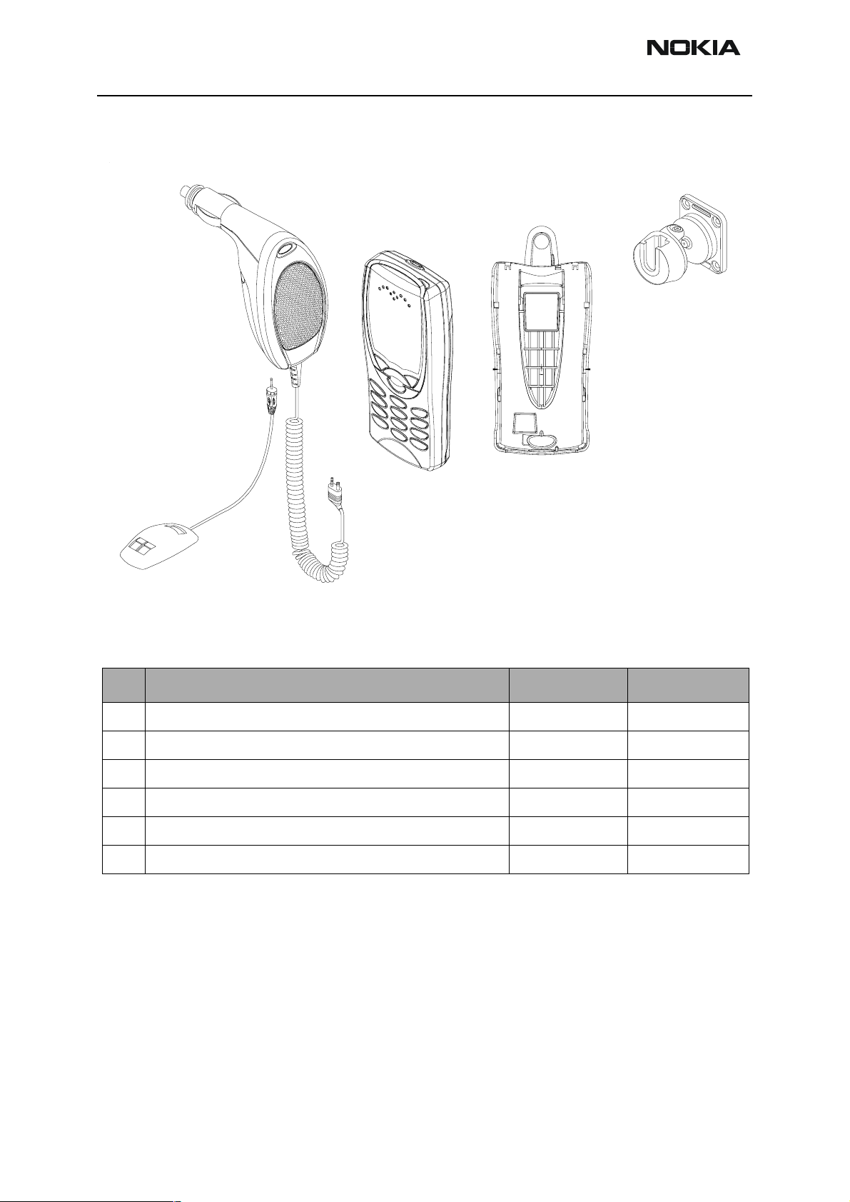
Express Car Kit (CARK-124) Option for Americas
5.
3.
1.
2.
4.
Figure 3: Express Car Kit (CARK-124)
Item Name: Type Code: Material Code:
Express Car Kit for Americas (Retail Pack) CARK-124 0080372
1. Transceiver (Not included, see Product Variants)
2. Pocket Clip SKB-2 0720218
3. Swivel Mount HHS-12 0620054
4. Hands Free Microphone HFM-8 0690016
5. Hands Free Cigarette Lighter Charger PPH-1 0675182
Page 6 ãNokia Mobile Phones Ltd. Issue 1 06/00
Page 13
NSB-7
PAMS Technical Documentation General Information
Product and Module List
Unit/Type: Product Code:
Transceiver NSB-7 See Product Variants
Standard Battery BLB-2 (Li-ion 650 mAh) 0670246
Standard Battery BLB-2 (Li-ion 650 mAh) for Americas 0670322
AC Travel Charger ACP-7E (EURO) 207-253 Vac 0675144
AC Travel Charger ACP-7U (US) 108-132 Vac 0675143
AC Travel Charger ACP-7C (US) 198-242 Vac 0675158
AC Travel Charger ACP-7X (UK) 207-253 Vac 0675145
AC Travel Charger ACP-7H (UK) 180-220 Vac 0675146
AC Travel Charger ACP-7A (AUS) 216-264 Vac 0675148
Performance Travel Charger ACP-8E (EURO) 90-264 Vac 0675195
Performance Travel Charger ACP-8K (KOREA) 90-264 Vac 0675199
Performance Travel Charger ACP-8X (UK) 90-264 Vac 0675197
Performance Travel Charger ACP-8U (US) 90-264 Vac 0675196
Performance Travel Charger ACP-8C (CHINA) 90-264 Vac 0675211
Performance Travel Charger ACP-8A (AUS) 90-264 Vac 0675214
Headset HDC-5 0694059
Loopset LPS-3 0630244
Pocket Clip SKB-2 0720218
Desk Stand DCV-1B 0675220
Swivel Mount HHS-12 0620054
HF Microphone HFM-8 0690016
Plug & Play HF Cigarette Lighter Charger PPH-1 0675182
Cigarette Lighter Charger LCH-8 0675231
Cigarette Lighter Charger LCH-9 0675120
Carrying Case CBK-3V 0272237
Carrying Case CBK-3H 0272236
Issue 1 06/00 ãNokia Mobile Phones Ltd. Page 7
Page 14
NSB-7
General Information PAMS Technical Documentation
Technical Specifications
General Specifications of Transceiver NSB-7
Parameter Unit
Cellular System GSM1900
RX frequency band 1930 ...1990 MHz
TX frequency band 1850 ...1910 MHz
Output power +0 ...+29 dBm / 1.0 mW ...1 W
Duplex spacing 80 MHz
Number of RF channels 299
Channel spacing 200 kHz
Number of TX power levels 16
Sensitivity, static channel -102 dBm
Frequency error, static channel < 0.1 ppm
RMS phase error < 5.0 ο
Peak phase error < 20.0 ο
Page 8 ãNokia Mobile Phones Ltd. Issue 1 06/00
Page 15

Programmes After Market Services
NSB-7 Series Transceivers
System Module
Issue 1 06/00 ãNokia Mobile Phones Ltd.
Page 16

NSB-7
System Module PAMS Technical Documentation
Table of Contents
Page No
System Module ........................................................................................................................1
Transceiver NSB-7 ................................................................................................................................... 6
Introduction ........................................................................................................................................... 6
Operational Modes ............................................................................................................................ 6
Interconnection Diagram ................................................................................................................... 7
System Module......................................................................................................................................... 8
Baseband Module ................................................................................................................................. 8
Block Diagram..................................................................................................................................... 8
Technical Summary ........................................................................................................................... 9
Technical Specifications ...................................................................................................................10
Absolute Maximum Ratings ........................................................................................................ 10
DC Characteristics .......................................................................................................................... 10
External and Internal Signals and Connections..................................................................... 10
DC (charger) connector ...............................................................................................................10
Service Connector .........................................................................................................................11
Battery connector .........................................................................................................................11
SIM card connector ......................................................................................................................12
RTC backup battery ......................................................................................................................12
Functional Description ......................................................................................................................13
Power Distribution.......................................................................................................................... 13
Battery Interface............................................................................................................................. 13
Battery charging ...........................................................................................................................14
Startup Charging ..........................................................................................................................14
Battery Overvoltage Protection ................................................................................................15
Battery Removal During Charging ...........................................................................................16
PWM .................................................................................................................................................16
Battery Identification ..................................................................................................................16
Battery Temperature ....................................................................................................................18
Supply Voltage Regulators .........................................................................................................19
Switched Mode Supply VSIM ....................................................................................................21
Power Up and Power Down ......................................................................................................... 22
Power up with charger ................................................................................................................22
Power Up with the Power Switch (PWRONX) ......................................................................23
Power Up by RTC ...........................................................................................................................24
Power Up by IBI .............................................................................................................................24
Power Down ...................................................................................................................................24
Modes of Operation ....................................................................................................................... 25
Acting Dead ....................................................................................................................................25
Active Mode ...................................................................................................................................25
Sleep Mode .....................................................................................................................................25
Charging ..........................................................................................................................................26
Watchdog .......................................................................................................................................26
Audio Control................................................................................................................................... 27
PCM serial interface ....................................................................................................................27
Digital Control ................................................................................................................................. 28
MAD2 WD1 .....................................................................................................................................28
Memories........................................................................................................................................... 37
Page 2 ãNokia Mobile Phones Ltd. Issue 1 06/00
Page 17

NSB-7
PAMS Technical Documentation System Module
MAD memory configuration ......................................................................................................37
Memory ...........................................................................................................................................37
Program and Data Memory .......................................................................................................37
Work Memory ................................................................................................................................37
MCU Memory Requirements .....................................................................................................37
MCU Memory Map .......................................................................................................................37
Flash Programming ......................................................................................................................38
COBBA GJP .....................................................................................................................................39
Real time clock ..............................................................................................................................40
RTC backup battery charging ....................................................................................................40
Security ............................................................................................................................................40
Baseband EMC Strategy .............................................................................................................40
Baseband Testing ..........................................................................................................................41
Alignments .....................................................................................................................................41
Baseband Startup for Testing ....................................................................................................42
RF Module............................................................................................................................................... 43
Shielding............................................................................................................................................ 43
Environmental Specifications .........................................................................................................43
Normal and Extreme voltages ...................................................................................................43
Temperature Conditions .............................................................................................................43
Humidity ..........................................................................................................................................43
Vibration ..........................................................................................................................................44
ESD Strength ..................................................................................................................................44
Main Technical Specifications ........................................................................................................44
Maximum Ratings .......................................................................................................................... 44
RF Frequency Plan ..............................................................................................................................45
DC Characteristics ..............................................................................................................................45
Regulators......................................................................................................................................... 45
Control Signals ................................................................................................................................ 46
Power Distribution Diagram ............................................................................................................47
RF Characteristics ...............................................................................................................................48
GSM1900 (PCS1900) ..................................................................................................................... 48
Transmitter Characteristics.......................................................................................................... 48
Output Power Requirements ....................................................................................................... 48
Output RF Spectrum due to modulation.................................................................................. 49
Spectrum due to switching transients...................................................................................... 49
Spurious Emissions (when allocated a channel).................................................................... 49
Spurious Emissions (idle mode) .................................................................................................. 50
Frequency Error and Phase Accuracy ........................................................................................ 50
Receiver Characteristics ...................................................................................................................50
Blocking Requirements ................................................................................................................. 51
AM Suppression Requirements ................................................................................................... 51
Sensitivity, Inter modulation, Spurious Rejection and Emissions..................................... 52
Reference Interference level........................................................................................................ 52
RF Block Diagram ...............................................................................................................................53
Frequency synthesizer .......................................................................................................................54
Receiver .................................................................................................................................................55
Transmitter ...........................................................................................................................................56
Issue 1 06/00 ãNokia Mobile Phones Ltd. Page 3
Page 18

NSB-7
System Module PAMS Technical Documentation
AGC strategy ........................................................................................................................................57
AFC function ........................................................................................................................................57
DC Compensation ...............................................................................................................................58
Parts List of RB9 (EDMS Issue 5.3) (Code: 0201512)................................................................ 59
Schematic Diagrams: RB9 (at the back of the binder)
Circuit Diagram of Power Supply (Version 05.21 Edit 64) for layout 5 ............................... A-1
Circuit Diagram of CPU Block (Version 05.21 Edit 45) for layout 5 ..................................... A-2
Connection between RF and Baseband modules (Version 05.21 Edit 37) for layout 5... A-3
Baseband Block Interconnections (Version 05.21 Edit 40) for layout 5 .............................. A-4
Circuit Diagram of MAD Block (Version 05.21 Edit 27) for layout 5 .................................... A-5
Circuit Diagram of RF Block (Version 05.21 Edit 132) for layout 5 ...................................... A-6
Circuit Diagram of UIF (Version 05.21 Edit 36) for layout 5................................................... A-7
Circuit Diagram of Audio and RFI (Version 05.21 Edit 72) for layout 5 .............................. A-8
Circuit Diagram of IR Module (Version 05.21 Edit 23) for layout 5 ..................................... A-9
Layout Diagram of RB9 -Top (Version 05.21)............................................................................A-10
Layout Diagram of RB9 - Bottom (Version 05.21)................................................................... A-10
Testpoints of RB9 - Top (Version 05.21) .....................................................................................A-11
Testpoints of RB9 - Bottom (Version 05.21)..............................................................................A-12
RF Testpoints for RB9 - Circuit Diagram (Version 05.21 Edit132 ) .....................................A-13
RF Testpoints of RB9 - Layout (Version 05.21) .........................................................................A-14
Page 4 ãNokia Mobile Phones Ltd. Issue 1 06/00
Page 19

NSB-7
PAMS Technical Documentation System Module
List of Figures
Page No
Fig 1 Block Diagram ...................................................................................................................................... 8
Fig 2 Block Diagram of Power Distribution ............................................................................................ 13
Fig 3 Charging Block Diagram.................................................................................................................... 14
Fig 4 Output Overvoltage Protection (in principle; not in time scale) ........................................... 15
Fig 5 Output Overvoltage Protection When Battery Removed (in principle)................................ 16
Fig 6 BSI connections for all battery types ............................................................................................ 17
Fig 7 SIMCardDetX Detection Levels........................................................................................................ 18
Fig 8 Standard Battery BTEMP connection ............................................................................................ 19
Fig 9 Principle of the SMR Power Functions.......................................................................................... 22
Fig 10 Power Up With Charger .................................................................................................................. 23
Fig 11 Power Up With Switch .................................................................................................................... 24
Fig 12 Flash Programming Sequence ....................................................................................................... 39
Fig 13 RF Frequency Plan............................................................................................................................. 45
Fig 14 Power Distribution Diagram .......................................................................................................... 47
Fig 15 RF Block Diagram.............................................................................................................................. 53
Fig 16 Phase Locked Loop............................................................................................................................ 55
Fig 17 Power Control Loop Diagram......................................................................................................... 57
Issue 1 06/00 ãNokia Mobile Phones Ltd. Page 5
Page 20

NSB-7
System Module PAMS Technical Documentation
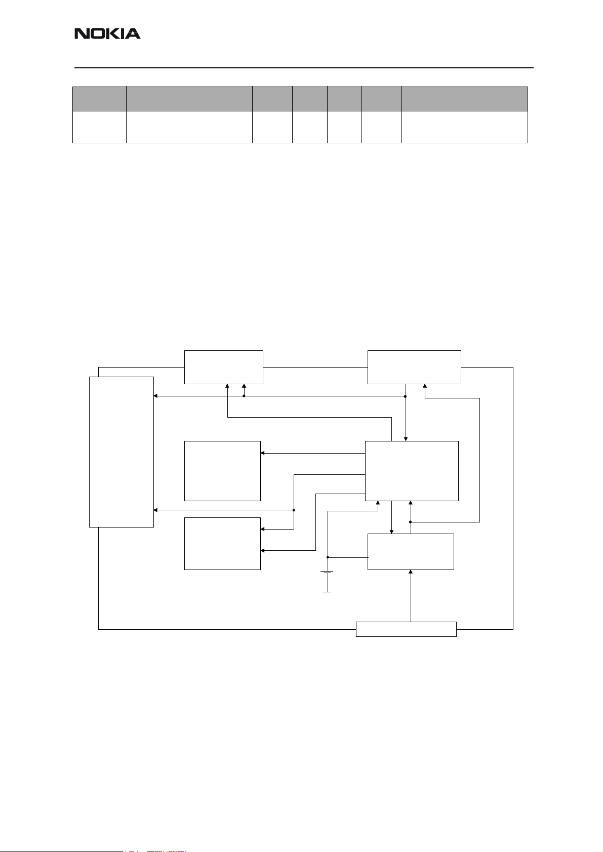
Transceiver NSB-7
Introduction
The NSB-7 is a single band transceiver unit designed for the GSM1900 networks. It is
GSM1900 power class 1 (1W) transceiver.
The transceiver consists of System/RF module (RB9), Display module (UX7) and assembly
parts.
The transceiver has a full graphic display and the user interface is based on a jack style
UI with two soft keys.
A back mounted antenna is used, there is no connection to an external antenna.
The transceiver has a low leakage tolerant earpiece and an omnidirectional microphone,
providing excellent audio quality. The transceiver supports full rate, an enhanced full rate
and a half rate speech decoding.
An integrated IR link provides a connection between two NSB-7 transceivers or a transceiver and a PC (internal data), or a transceiver and a printer.
The small SIM (Subscriber Identity Module) card is located under the back cover of the
phone.
Operational Modes
There are five different operational modes:
• power off mode
•idle mode
• active mode
• charge mode
• local mode
In the power off mode only the circuits needed for power up are supplied.
In the idle mode circuits are powered down and only the sleep clock is running.
In the active mode all the circuits are supplied with power although some parts might be
in idle state part of the time.
The charge mode is effective in parallel with all previous modes. The charge mode itself
consists of two different states, i.e. the fast charge and the maintenance mode.
Page 6 ãNokia Mobile Phones Ltd. Issue 1 06/00
Page 21
NSB-7
PAMS Technical Documentation System Module
The local mode is used for alignment and testing.
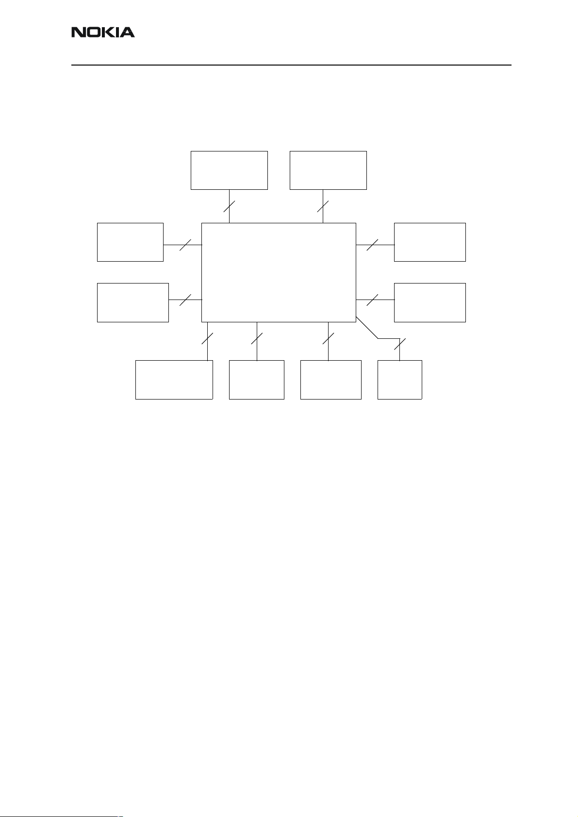
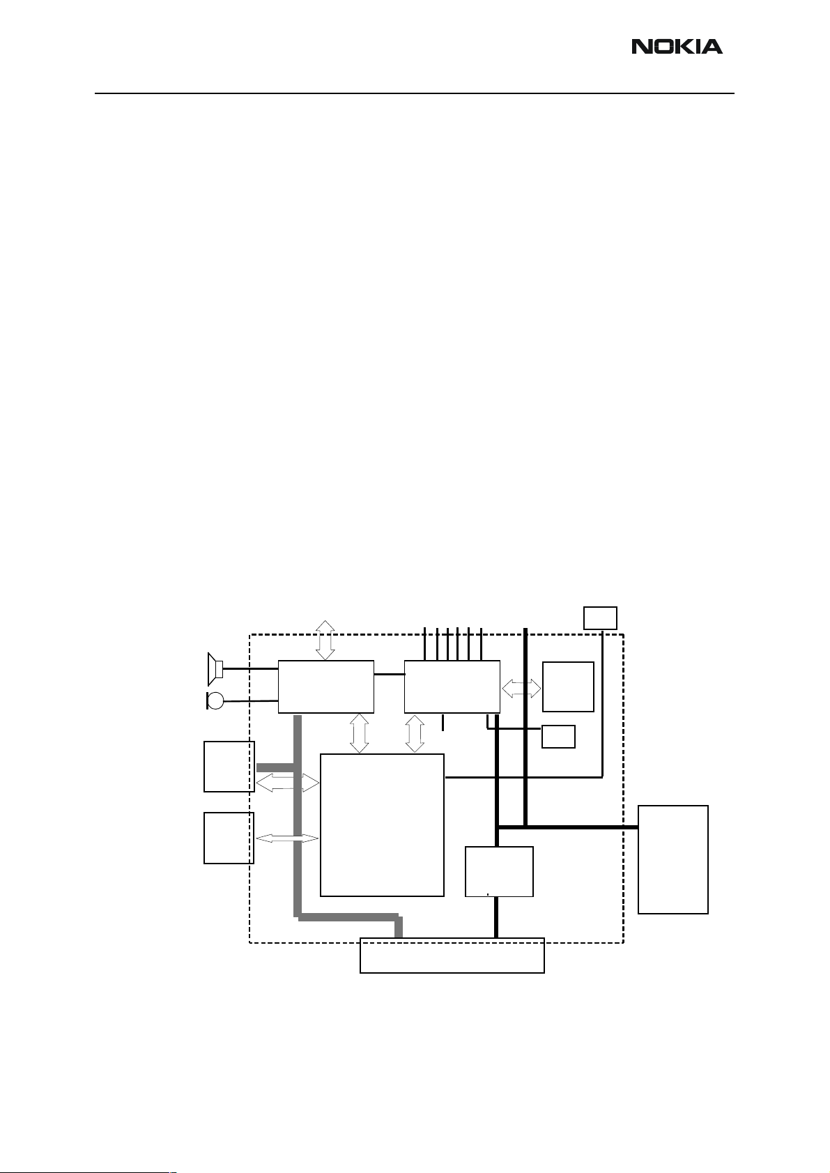
Interconnection Diagram
Keyboard LCD module
14 9
SIM
Antenna
Microphone IR Link Earpiece HF/HS
6
4
Battery
Radio
Module
2
RB9
2+2
Charger
2824
Issue 1 06/00 ãNokia Mobile Phones Ltd. Page 7
Page 22
NSB-7
System Module PAMS Technical Documentation
System Module
Baseband Module
The ASICs are in the uBGA package. Flash and SRAM chips are inside the same package.
EEPROM is software emulated with Flash. These changes have decreased the number of
I/O between the ICs. Smaller I/O count has made using smaller packages possible
The baseband architecture supports a power saving function called ”sleep mode”. This
sleep mode shuts off the VCTCXO, which is used as system clock source for both RF and
baseband. During the sleep mode the system runs from a 32 kHz crystal. The phone is
waken up by a timer running from this 32 kHz clock supply. The sleeping time is determined by some network parameters. The sleep mode is entered when both the MCU and
the DSP are in stand-by mode and the normal VCTCXO clock has been switched off.
The battery charging is controlled by a PWM signal from the CCONT. The PWM duty cycle
is determined by a charging software and is fed to the CHAPS charging switch.
Two types of chargers can be connected to the phone. Standard chargers (two wires)
provide a coarse supply power, which is switched by the CHAPS for suitable charging
voltage and current. Advanced chargers (three wires) are equipped with a control input.
Three wire chargers are treated like two wire ones.
Block Diagram
TX/RX SIGNALS
COBBA SUPPLY
COBBA
UI
MAD
IR
+
MEMORIES
RF SUPPLIES
CCONT
BB SUPPLY
CHAPS
PA SUPPLY
SLEEP CLOCK
32kHz
CLK
VBAT
SIM
13MHz
CLK
SYSTEM CLOCK
BATTERY
BASEBAND
EXT. AUDIO
HS-connector
Charger
connector
Figure 1: Block Diagram
Page 8 ãNokia Mobile Phones Ltd. Issue 1 06/00
Page 23

NSB-7
PAMS Technical Documentation System Module
Technical Summary
The baseband module consists of four ASICs; CHAPS, CCONT, COBBA-GJP and
MAD2WD1, which take care of the baseband functions of the engine.
The baseband is running from a 2.8V power rail, which is supplied by a power controlling
ASIC CCONT. MAD2WD1 supply voltages are VBB and VCORE (V2V), VBB feed I/O pins so
that MAD2WD1 is externally fully compatible with old versions. VCORE feed MAD2WD1
internal functions supply voltage; CPU, DSP and system logic. In the CCONT there are 6
individually controlled regulator outputs for RF-section and two outputs for the baseband. In addition there is one +5V power supply output (V5V). The CCONT contains also a
SIM interface, which supports both 3V and 5V SIM-cards. A real time clock function is
integrated into the CCONT, which utilizes the same 32kHz clock supply as the sleep
clock. A backup power supply is provided for the RTC, which keeps the real time clock
running when the main battery is removed. The backup power supply is a rechargable
battery. The backup time with the battery is ten minutes minimum.
The analog interface between the baseband and the RF section is handled by a COBBA
ASIC. COBBA provides A/D and D/A conversion of the in-phase and quadrature receive
and transmit signal paths and also A/D and D/A conversions of received and transmitted
audio signals to and from the user interface. The COBBA supplies the analog TXC and AFC
signals to RF section according to the MAD DSP digital control. Data transmission
between the COBBA and the MAD is implemented using serial bus for high speed signalling and for PCM coded audio signals. Digital speech processing is handled by the MAD
ASIC. COBBA is a dual voltage circuit, the digital parts are running from the baseband
supply VBB and the analog parts are running from the analog supply VCOBBA.
The baseband supports both internal and external microphone inputs and speaker outputs. Input and output signal source selection and gain control is done by the COBBA
according to control messages from the MAD. Keypad tones, DTMF and other audio tones
are generated and encoded by the MAD and transmitted to the COBBA for decoding. A
buzzer and an external vibra alert control signals are generated by the MAD with separate PWM outputs.
EMC shielding is implemented using a metallized plastic frame. On the other side the
engine is shielded with PCB grounding. Heat generated by the circuitry will be conducted
out via the PCB ground planes.
Issue 1 06/00 ãNokia Mobile Phones Ltd. Page 9
Page 24
NSB-7
System Module PAMS Technical Documentation
Technical Specifications
Absolute Maximum Ratings
Parameter Rating
Battery voltage -0.3... 5.3 V
Charger input voltage -5.0... 16V
DC Characteristics
Line Symbol Minimum
Supply battery voltage 3.0 3.9 4.8 V
Battery powerup voltage (HW) 2.9 3.0 3.1 V
Battery cut off voltage (HW) 2.7 2.8 2.9 V (3.1 V SW cutoff)
Regulated baseband supply voltage
Regulated baseband supply current
COBBA analog supply voltage 2.7 2.8 2.85 V
COBBA analog supply current 5 20 100 mA
Regulated 5V supply voltage 4.8 5.0 5.2 V
Regulated 5V supply current 0 1 30 mA
Regulated 5V SIM supply voltage 4.8 5.0 5.2 V
Regulated 5V SIM supply current 3 10 30 mA
Regulated 3V SIM supply voltage 2.8 3.0 3.2 V
2.7 2.8 2.85 V
3 50 125 mA
Typical /
Nominal
Maximum Unit / Notes
Regulated 3V SIM supply current 1 6 30 mA
Voltage reference 1.4775 1.5 1.5225 V
External and Internal Signals and Connections
This section describes the external electrical connection and interface levels on the baseband. The electrical interface specifications are collected into tables that covers a connector or a defined interface.
DC (charger) connector
DC (charger) connector is physically integrated in the same component with the acces-
Page 10 ãNokia Mobile Phones Ltd. Issue 1 06/00
Page 25
NSB-7
PAMS Technical Documentation System Module
sory interface connector. DC connector has both jack and contact pads for desk stand.
Name Min Typ Max Unit Notes
VIN 0 12 V
0850mA
L_GND 0 0.3 V
Service Connector
Name Parameter Min Typ Max Unit Remark
MBUS Serial clock from
the Prommer
FBUS_RX Serial data from the
Prommer
FBUS_TX Data acknowledge
to the Prommer
GND GND 0 0 V Ground
0
2.0
0
2.0
0
2.0
logic low
logic low
logic low
logic high
logic low
logic high
0.8
2.85
0.8
2.85
0.5
2.85
V Prommer detection and Serial
Clock for synchronous communication
V Receive Data from Prommer to
Baseband
V Transmit Data from Baseband to
Prommer
The service connector is used as a flash programming interface for updating (i.e. re-programming) the flash program memory and an electrical access for services to the engine.
When the flash prommer is connected to the phone supply power is provided through the
battery contacts and the phone is powered up with a pulse given to the BTEMP line.
Battery connector
The BSI contact on the battery connector is used to detect when the battery is to be
removed to be able to shut down the operations of the SIM card before the power is lost
if the battery is removed with power on. The BSI contact disconnects earlier than the
supply power contacts to give enough time for the SIM and LCD shut down.
Name Min Typ Max Unit Notes
VBATT 3.0 3.9 4.2 V Battery voltage
BSI 0 2.85 V Battery size indication
Phone has 100kohm pull-up resistor.
SIM Card removal detection
(Threshold is 2.4V@VBB=2.8V)
68 kohm Battery indication resistor (BLB-2)
kohm Battery indication resistor (service battery)
Issue 1 06/00 ãNokia Mobile Phones Ltd. Page 11
Page 26
NSB-7
System Module PAMS Technical Documentation
Name Min Typ Max Unit Notes
BTEMP 0 1.4 V Battery temperature indication
Phone has a 100k (+/-5%) pull-up resistor,
Battery package has a NTC pull-down
resistor: 47k +/-5%@+25C, B=4050 +/3%
2.1
510330
0 1 kohm Local mode initialization (in production)
BGND 0 0 V Battery ground
V
ms
Phone power up by battery (input)
Power up pulse width
SIM card connector
The SIM card connector is located on the engine beside the battery pack.
Pin Name Parameter Min Typ Max Unit Notes
4GND GND 0 0 V Ground
3, 5 VSIM 5V SIM Card
3V SIM Card
6 DATA 5V Vin/Vout
3V Vin/Vout
2 SIMRST 5V SIM Card
3V SIM Card
4.8
2.8
4.0
0
2.8
0
4.0
2.8
5.0
3.0
“1”
“0”
“1”
“0”
“1”
“1”
5.2
3.2
VSIM
0.5
VSIM
0.5
VSIM
VSIM
V Supply voltage
VSIM data
Trise/Tfall max 1us
VSIM reset
1SIMCLKFrequency
Trise/Tfall
3.25
25
MHz
ns
SIM clock
RTC backup battery
The RTC block in CCONT needs a power backup to keep the clock running when the
phone battery is disconnected. The backup power is supplied from a rechargable Li-ion
battery that can keep the clock running ten minutes minimum. The backup battery is
charged from the main battery through CHAPS.
Signal Parameter Min Typ Max Unit Notes
VBACK Backup battery charging
from CHAPS
Backup battery charging
from CHAPS
VBACK Backup battery supply to
CCONT
3.02 3.15 3.28 V
100 200 500 uA Vout@VBAT-0.2V
23.28V
Page 12 ãNokia Mobile Phones Ltd. Issue 1 06/00
Page 27
NSB-7
PAMS Technical Documentation System Module
Signal Parameter Min Typ Max Unit Notes
Backup battery supply to
CCONT
Functional Description
Power Distribution
In normal operation the baseband is powered from the phone‘s battery. The battery consists of one Lithium-Ion cell. An external charger can be used for recharging the battery
and supplying power to the phone.
The baseband contains parts that control power distribution to whole phone excluding
those parts that use continuous battery supply. The battery feeds power directly to the
CCONT and UI (buzzer and display and keyboard lights).
The power management circuit CHAPS provides protection against over voltages, charger
failures and pirate chargers etc. that would otherwise cause damage to the phone.
RF
UI
(LCD,
backlights,
buzzer)
80 uA
RF supply voltages
VCobba
Vbb
Battery connector
VB
CCONTCOBBA GJP
Baseband
MAD2 +
MEMORY
CHRG_CTRL
VCORE
CHAPS
RTC backup
VChar
Charger & headset connector
Vbatt
Figure 2: Block Diagram of Power Distribution
Battery Interface
Issue 1 06/00 ãNokia Mobile Phones Ltd. Page 13
Page 28
NSB-7
System Module PAMS Technical Documentation
Battery charging
The electrical specifications give the idle voltages produced by the acceptable chargers
at the DC connector input. The absolute maximum input voltage is 30V due to the transient suppressor that is protecting the charger input. At phone end there is no difference
between a plug-in charger or a desktop charger. The DC-jack pins and bottom connector
charging pads are connected together inside the phone.
MAD
MAD
VBAT
CCONTINT
CCONT
0R22
GND
ICHAR
PWM_OUT
VCHAR
LIM
VOUT
CHAPS
RSENSE
PWM
VCH
GND
22k
TRANSCEIVER
1u
100k
1n
10k
Figure 3: Charging Block Diagram
30V
CHARGER
2A
VIN
L_GND
Startup Charging
When a charger is connected, the CHAPS is supplying a startup current minimum of
130mA to the phone. The startup current provides initial charging to a phone with an
empty battery. Startup circuit charges the battery until the battery voltage level is
reaches 3.0V (+/- 0.1V) and the CCONT releases the PURX reset signal and program execution starts. Charging mode is changed from startup charging to PWM charging that is
controlled by the MCU software. If the battery voltage reaches 3.55V (3.75V maximum)
before the program has taken control over the charging, the startup current is switched
off. For accessory detection, startup current is possible cut via CCUT line. The startup
current is switched on again when the battery voltage is sunken 100mV (nominal).
Parameter Symbol Min Typ Max Unit
VOUT Start-up mode cutoff limit Vstart 3.45 3.55 3.75 V
VOUT Start-up mode hysteresis
NOTE: Cout=4.7 uF
Start-up regulator output current
VOUT=0V....Vstart
Vstarthys 80 100 200 mV
Istart 130 165 200 mA
Page 14 ãNokia Mobile Phones Ltd. Issue 1 06/00
Page 29
NSB-7
PAMS Technical Documentation System Module
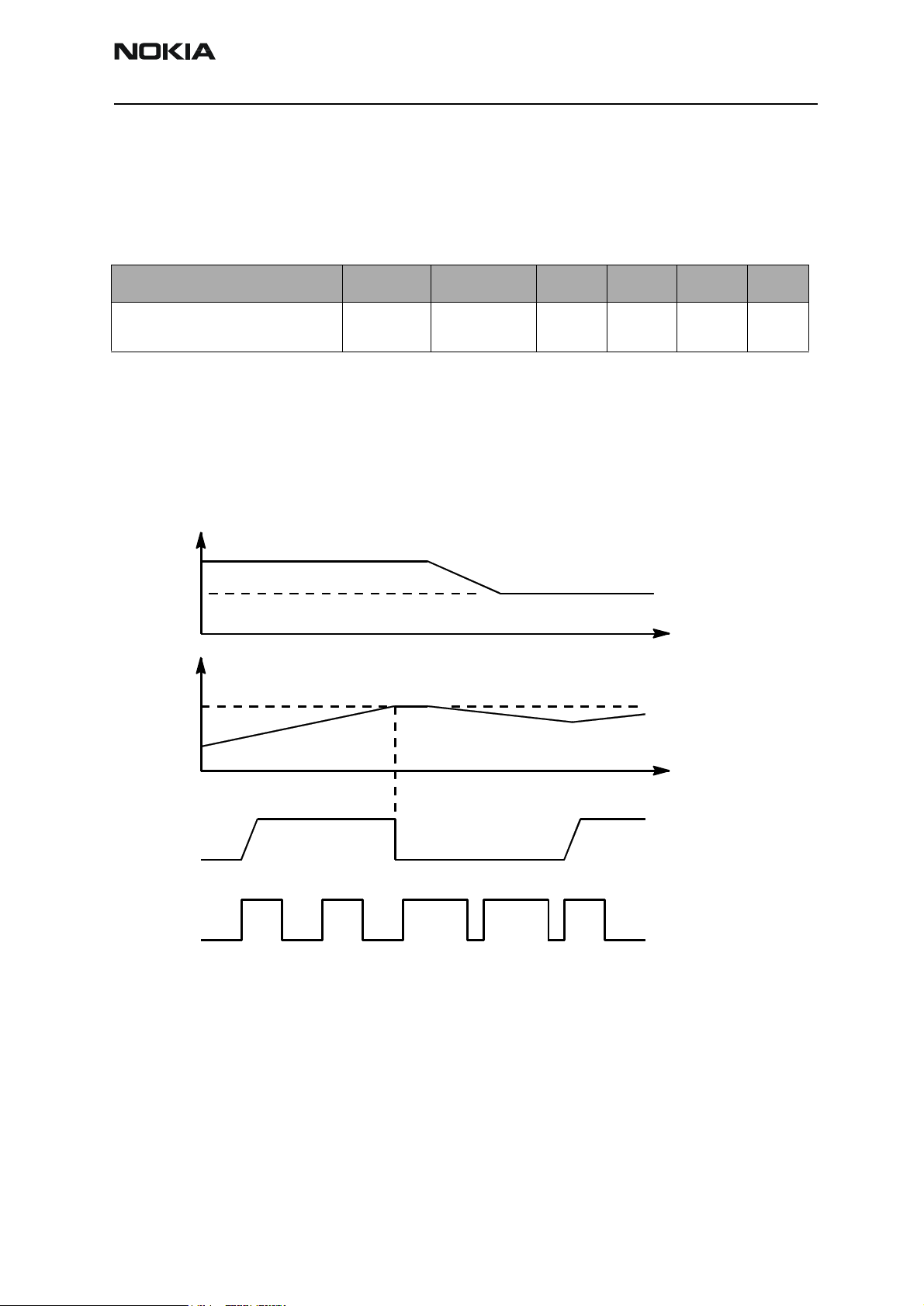
Battery Overvoltage Protection
Output overvoltage protection is used to protect phone from damage. This function is
also used to define the protection cutoff voltage for the Lithium-Ion battery. The power
switch is immediately turned OFF if the voltage in VOUT rises above the selected limit
VLIM.
Parameter Symbol LIM input Min Typ Max Unit
Output voltage cutoff limit (during transmission or Li-battery)
VLIM LOW 4.4 4.6 4.8 V
The voltage limit (VLIM1 or VLIM2) is selected by logic LOW or logic HIGH on the CHAPS
(N101) VLIM input pin.
When the switch in output overvoltage situation has once turned OFF, it stays OFF until
the battery voltage falls below VLIM and PWM = LOW is detected. The switch can be
turned on again by setting PWM = HIGH.
VCH
VCH<VOUT
t
VOUT
VLIM
SWITCH
PWM (32Hz)
t
ON OFF
Figure 4: Output Overvoltage Protection (in principle; not in time scale)
ON
Issue 1 06/00 ãNokia Mobile Phones Ltd. Page 15
Page 30
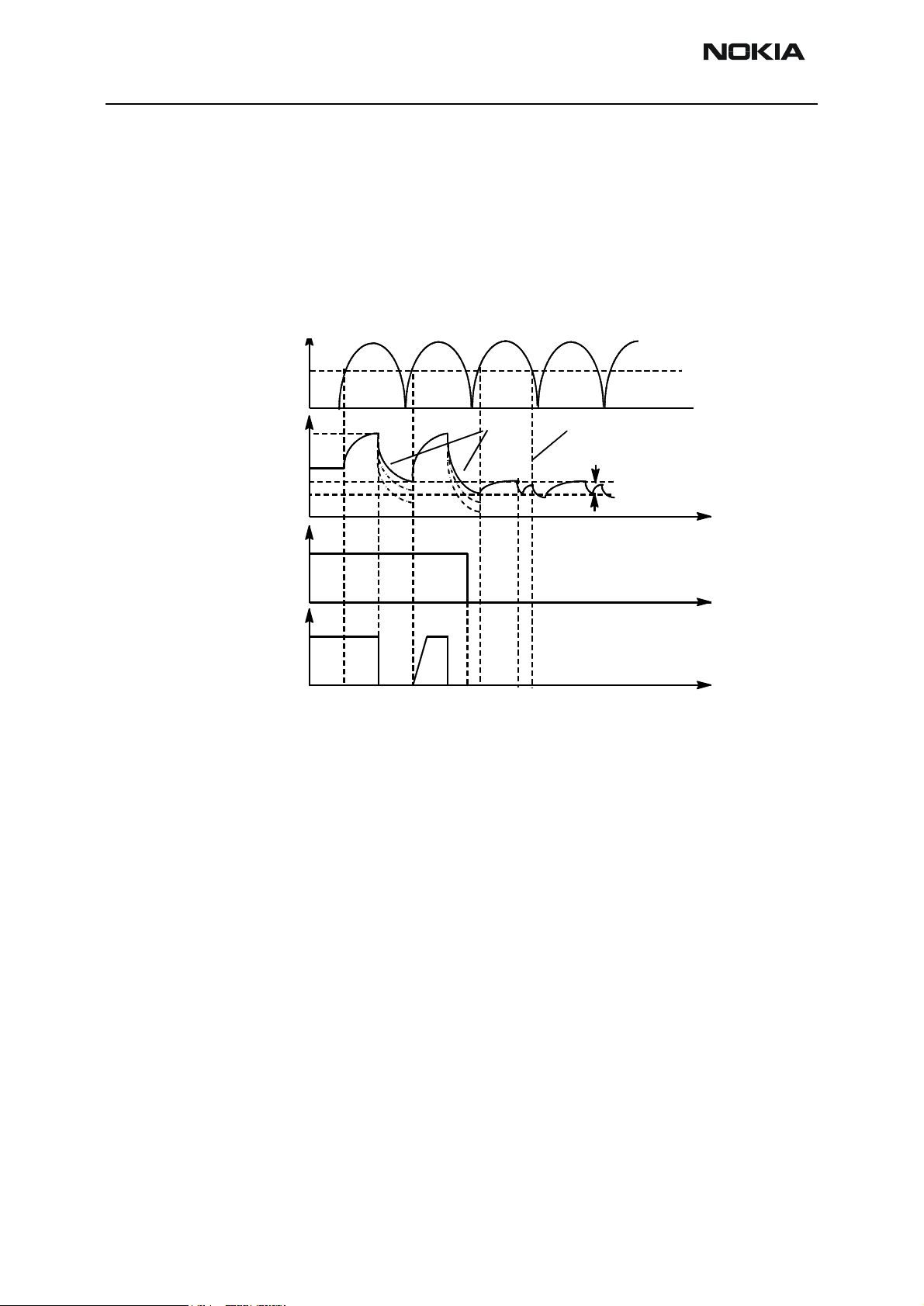
NSB-7
"1"
3
4
5
6
7
System Module PAMS Technical Documentation
Battery Removal During Charging
Output overvoltage protection is also needed in case the main battery is removed when
charger connected or charger is connected before the battery is connected to the phone.
With a charger connected, if VOUT exceeds VLIM, CHAPS turns switch OFF until the
charger input has sunken below Vpor (nominal 3.0V, maximum 3.4V). MCU software will
stop the charging (turn off PWM) when it detects that battery has been removed. The
CHAPS remains in protection state as long as PWM stays HIGH after the output overvoltage situation has occured.
VCH
(Standard
Charger)
VOUT
PWM
SWITCH
Vpor
Droop depends on load
VLIM
4V
Vstart
0
ON
OFF
1
Battery removed, (standard) charger connected, VOUT rises (follows charger voltage)
2. VOUT exceedslimit VLIM(X),switch is turned immediatelyOFF
3
VOUT falls (because no battery) , also VCH<Vpor (standard chargers full-rectified
output).WhenVCH>VporandVOUT<VLIM(X)->switchturnedonagain(alsoPWM
is still HIGH) a nd VOUT again exceeds VLIM(X).
4. Software sets PWM = LOW -> CHAPS does n ot enter PWM mode
5. PWM low -> Startup mode, startup current flows until Vstart limit reached
6. VOUT exceeds limit Vstart, Istart is turned off
7. VCH falls below Vpor
2
1
& C in phone
Istart off due to VCH<Vpor
Vstarthys
t
t
t
Figure 5: Output Overvoltage Protection When Battery Removed (in principle; not in time scale)
PWM
When a charger is used, the power switch is turned ON and OFF by the PWM input. PWM
rate is 1Hz. When PWM is HIGH, the switch is ON and the output current Iout = charger
current - CHAPS supply current. When PWM is LOW, the switch is OFF and the output
current Iout = 0. To prevent the switching transients inducing noise in audio circuitry of
the phone soft switching is used.
Battery Identification
Different battery types are identified by a pulldown resistor inside the battery pack. The
BSI line inside transceiver has a 100k pull-up to VBB. The MCU can identify the battery
Page 16 ãNokia Mobile Phones Ltd. Issue 1 06/00
Page 31

NSB-7
PAMS Technical Documentation System Module
by reading the BSI line DC-voltage level with a CCONT (N100) A/D-converter.
Name Min Typ Max Unit Notes
BSI 0 2.8 V Battery size indication 100k pull-up resistor to
VBB in phone
SIM Card removal detection (Threshold is
2.4V@VBB=2.8V)
68 kohm Indication of a BLB-2 battery (600mAh Li-Ion)
22 kohm Indication resistor for a service battery
-5 5 % Indication resistor and pull-up resistor tolerance
VBATT
BATTERY
BTEMP
BSI
R
s
BGND
2.8V
10n
100k
10k
TRANSCEIVER
BSI
SIMCardDetX
CCONT
MAD
Figure 6: BSI connections for all battery types
The battery identification line is used also for battery removal detection. The BSI line is
connected to a SIMCardDetX line of MAD2. SIMCardDetX is a threshold detector with a
nominal input switching level 0.85xVcc for a rising edge and 0.55xVcc for a falling edge.
The battery removal detection is used as a trigger to power down the SIM card before the
power is lost. The BSI contact in the battery contact disconnects before the other con-
Issue 1 06/00 ãNokia Mobile Phones Ltd. Page 17
Page 32

NSB-7
System Module PAMS Technical Documentation
tacts so that there is a delay between battery removal detection and supply power off.
Vcc
0.85 _ 0.05 Vcc
0.55 _ 0.05 Vcc
SIMCARDDETX
GND
Figure 7: SIMCardDetX Detection Levels
SigOut
Battery Temperature
The battery temperature is measured with a NTC inside the battery pack. The BTEMP line
inside transceiver has a 100k pull-up to VREF. The MCU can calculate the battery temperature by reading the BTEMP line DC-voltage level with a CCONT (N100) A/D-converter.
Pin Name Min Typ Max Unit Notes
3 BTEMP 0 1.4 V Battery temperature indication 100k pull-up
resistor to VREF in phone
Battery package has NTC pull-down resistor: 47k
+/-5%@+25C, B=4050 +/-3%
2.1
510320
47 Kohm Service battery value
-5 5 % 100k pull-up resistor tolerance
V
ms
Phone power up by battery (input)
Power up pulse width
Page 18 ãNokia Mobile Phones Ltd. Issue 1 06/00
Page 33

NSB-7
PAMS Technical Documentation System Module
VBATT
BATTERY
R
NTC
BSI
BTEMP
T
BGND
TRANSCEIVER
VREF
100k
10k
BTEMP
CCONT
Based on 47 kohm ± 5 % NTC with B = 4090 ±1.5 %. Without any alignment, with that
and 1 % pull-up resistor, ± 2.5 _C accuracy is achieved between - 20 and +60 _C (± 3.5
_C @ -40 ... +85 _C).
Supply Voltage Regulators
The heart of the power distribution is the CCONT. It includes all the voltage regulators
and feeds the power to the whole system. The baseband digital parts are powered from
the VBB regulator which provides 2.8V baseband supply. The baseband regulator is active
always when the phone is powered on. The VBB baseband regulator feeds MAD and
memories, VCORE for MAD core, COBBA digital parts and the LCD driver in the UI section.
There is a separate regulator for a SIM card. The regulator is selectable between 3V and
5V and controlled by the SIMPwr line from MAD to CCONT. The COBBA analog parts are
powered from a dedicated 2.8V supply VCOBBA. The CCONT supplies also 5V for RF and
for flash VPP. The CCONT contains a real time clock function, which is powered from a
RTC backup when the main battery is disconnected. The RTC backup is rechargable polyacene battery. The battery is charged from the main battery voltage by the CHAPS when
the main battery voltage is over 3.2V.
Figure 8: Standard Battery BTEMP connection
Operating Mode Vref RF REG VCOBBA VBB VSIM SIMIF Vcore
Power off Off Off Off Off Off Pull-down Off
Power on On On/Off On On On On/Off On
Reset On Off
On On Off Pull-down On
VR1 On
Sleep On Off Off On On On/Off On
Issue 1 06/00 ãNokia Mobile Phones Ltd. Page 19
Page 34

NSB-7
System Module PAMS Technical Documentation
NOTE: COBBA regulator is off in SLEEP mode. Its output pin may be fed from VBB
in SLEEP mode by setting bit RFReg(5) to’1’ (default).
CCONT includes also five additional 2.8V regulators providing power to the RF section.
These regulators can be controlled either by the direct control signals from MAD or by
the RF regulator control register in CCONT which MAD can update. Below are the listed
the MAD control lines and the regulators they are controlling.
- TxPwr controls VTX regulator (VR5)
- RxPwr controls VRX regulator (VR2)
- SynthPwr controls all the rf regulators except VR1
- VCXOPwr controls VXO regulator (VR1)
CCONT generates also a 1.5 V reference voltage VREF to COBBA. The VREF voltage is also
used as a reference to some of the CCONT A/D converters.
In addition to the above mentioned signals MAD includes also TXP control signal which
goes to HAGAR power control block. The transmitter power control TXC is led from
COBBA to HAGAR.
Characteristics Condition Min Typ Max Unit
Output current VR1-VR6 Vout@2.8V 100 mA
Output current VR7
Depends on external BJT
Output current VR7BASE
Base current limit
Output current VBB On
Current limit 250mA
Output current VBB Sleep
Current limit 5mA
Output voltage VR1-VR7 over full temperature, input
Output voltage VBB over full temperature, input
Output voltage V2V
(VCORE)
Vout@2.8V 150 mA
Vout@2.8V -10 mA
Vout@2.8V
Vout@2.8V
voltage and load range
voltage and load range
Programmable:
Vout=1.3V+225mV*n
N = 0,1,2,3,4,5,6
2.7 2.8 2.85 V
2.7 2.8 2.85 V
1.30 2.65 V
125
1
mA
mA
Output voltage V2V
(VCORE) tolerance
Line regulation (not VBB) F v 10kHz, 2)
VBAT>3.15V
-5 +5 %
49 DB
Page 20 ãNokia Mobile Phones Ltd. Issue 1 06/00
Page 35

NSB-7
PAMS Technical Documentation System Module
Characteristics Condition Min Typ Max Unit
Line regulation (not VBB) F v 100kHz, 2)
VBAT>3.15v
Line regulation VBB, V2V
(VCORE)
Load regulation T = 25_C0.61mV/mA
Supply current (each regulator) VR1...VR7
Supply current VBB ON mode I
Supply current VBB SLEEP mode I
Output voltage V2V
(VCORE)
F v 100kHz 2) 30 DB
ON mode I
MAD2WD1 C10
MAD2WD1 C07
MAD2WD1 C05
40 DB
/
out
60+330
/60+
out
250
/60+
out
100
2.65
1.75
1.75
I
/
out
10+540
I
/10+
out
400
I
/10+
out
150
mA
mA
mA
V
NOTE 1: Characteristics above are NOT valid if Vbat < 3.0V.
NOTE 2: Line regulation is 20dB for f<100kHz when battery voltage is lower than 3.1V.
Switched Mode Supply VSIM
There is a switched mode supply for SIM-interface. SIM voltage is selected via serial IO.
The 5V SMR can be switched on independently of the SIM voltage selection, but can’t be
switched off when VSIM voltage value is set to 5V.
Characteristics Condition Min Typ Max Unit
Output voltage VSIM Over temperature
Over current
Output voltage V5V Over temp & current 4.8 5.0 5.2 V
Output voltage V5V_2 Over temperature 5.0 6.0 V
Output current VSIM Continuous DC 30 mA
Output current V5V Continuous DC 30 mA
Current consumption VSIM on
sleep
2.8
4.8
3.0
5.0
200
100
3.2
5.2
330
150
NOTE: VSIM and V5V can give together a total of 30mA.
V
uA
uA
Issue 1 06/00 ãNokia Mobile Phones Ltd. Page 21
Page 36

NSB-7
System Module PAMS Technical Documentation
In the next figure the principle of the SMR / VSIM-functions is shown.
CCONT External
VBAT
V5V_4
V5V_3
V5V_2
VSIM
Power Up and Power Down
The baseband is powered up by:
1 Pressing the power key, that generates a PWRONX interrupt signal from the
power key to the CCONT, which starts the power up procedure.
2 Connecting a charger to the phone. The CCONT recognizes the charger from the
VCHAR voltage and starts the power up procedure.
3 A RTC interrupt. If the real time clock is set to alarm and the phone is switched
off, the RTC generates an interrupt signal, when the alarm is gone off. The RTC interrupt
signal is connected to the PWRONX line to give a power on signal to the CCONT just like
the power key.
5V reg
V5V
Figure 9: Principle of the SMR Power Functions
5V
5/3V
4 A battery interrupt. Intelligent battery packs have a possibility to power up the
phone. When the battery gives a short (10ms) voltage pulse through the BTEMP pin, the
CCONT wakes up and starts the power on procedure.
Power up with charger
When the charger is connected CCONT will switch on the CCONT digital voltage as soon
as the battery voltage exceeds 3.0V. The reset for CCONT’s digital parts is released when
the operating voltage is stabilized (50 us from switching on the voltages). Operating
voltage for VCXO is also switched on. The counter in CCONT digital section will keep
MAD in reset for 62 ms (PURX) to make sure that the clock provided by VCXO is stable.
After this delay MAD reset is released, and VCXO -control (SLEEPX) is given to MAD. The
next diagram explains the power on procedure with charger (the picture assumes empty
Page 22 ãNokia Mobile Phones Ltd. Issue 1 06/00
Page 37

NSB-7
PAMS Technical Documentation System Module
battery, but the situation would be the same with full battery):
SLEEPX
PURX
CCPURX
Vbat
VR6
VR1
VBB (2.8V)
Vchar
Vref
12 3
1: Battery voltage over 3.0==>Digital voltages to CCONT (VBB)
2: CCONT digital reset released. VCXO turned on
3: 62ms delay before PURX released
Figure 10: Power Up With Charger
When the phone is powered up with an empty battery pack using the standard charger,
the charger may not supply enough current for standard powerup procedure and the
powerup must be delayed.
Power Up with the Power Switch (PWRONX)
When the power on switch is pressed the PWRONX signal will go low. CCONT will switch
on the CCONT digital section and VCXO as was the case with the charger driven power
up. If PWRONX is low when the 64 ms delay expires, PURX is released and SLEEPX control
goes to MAD. If PWRONX is not low when 64 ms expires, PURX will not be released, and
Issue 1 06/00 ãNokia Mobile Phones Ltd. Page 23
Page 38

NSB-7
System Module PAMS Technical Documentation
CCONT will go to power off (digital section will send power off signal to analog parts)
SLEEPX
PURX
CCPURX
PWRONX
VR1,VR6
VBB (2.8V)
Vchar
12 3
1:Power switch pressed ==> Digital voltages on in CCONT (VBB)
2: CCONT digital reset released. VCXO turned on
3: 62 ms delay to see if power switch is still pressed.
Power Up by RTC
RTC (internal in CCONT) can power the phone up by changing RTCPwr to logical 1.
Power Up by IBI
IBI can power CCONT up by giving a short pulse (10ms) through the BTEMP line. After
powerup BTEMP will act as any other input channel for ADC.
When the PURX reset is released, the MAD releases the system reset ExtSysResetX and
the internal MCUResetX signals and starts the boot program execution from MAD
bootrom if MAD GenSDIO pin is pulled low or from external memory if GenSDIO pin is
pulled high. In normal operation the program execution continues from the flash program memory. If the MBUS line is pulled low during the power up the bootrom starts a
flash programming sequence and waits for the prommer response through FBUS_RX line.
Power Down
The baseband is powered down by:
1 Pressing the power key, that is monitored by the MAD, which starts the power
down procedure.
Figure 11: Power Up With Switch
2 If the battery voltage is dropped below the operation limit, either by not charging
it or by removing the battery.
3 Letting the CCONT watchdog expire, which switches off all CCONT regulators and
Page 24 ãNokia Mobile Phones Ltd. Issue 1 06/00
Page 39

NSB-7
PAMS Technical Documentation System Module
the phone is powered down.
4 Setting the real time clock to power off the phone by a timer. The RTC generates
an interrupt signal, when the alarm is gone off. The RTC interrupt signal is connected to
the PWRONX line to give a power off signal to the CCONT just like the power key.
The power down is controlled by the MAD. When the power key has been pressed long
enough or the battery voltage is dropped below the limit the MCU initiates a power
down procedure and disconnects the SIM power. Then the MCU outputs a system reset
signal and resets the DSP. If there is no charger connected the MCU writes a short delay
to CCONT watchdog and resets itself. After the set delay the CCONT watchdog expires,
which activates the PURX and all regulators are switched off and the phone is powered
down by the CCONT.
If a charger is connected when the power key is pressed the phone enters into the acting
dead mode.
Modes of Operation
Acting Dead
If the phone is off when the charger is connected, the phone is powered on but enters a
state called ”acting dead”. To the user the phone acts as if it was switched off. A battery
charging alert is given and/or a battery charging indication on the display is shown to
acknowledge the user that the battery is being charged.
Active Mode
In the active mode the phone is in normal operation, scanning for channels, listening to
a base station, transmitting and processing information. All the CCONT regulators are
operating. There are several sub-states in the active mode depending on if the phone is
in burst reception, burst transmission, if DSP is working etc.
Sleep Mode
In the sleep mode all the regulators except the baseband VBB and the SIM card VSIM
regulators are off. Sleep mode is activated by the MAD after MCU and DSP clocks have
been switched off. The voltage regulators for the RF section are switched off and the
VCXO power control, VCXOPwr is set low. In this state only the 32 kHz sleep clock oscillator in CCONT is running. The flash memory power down input is connected to the ExtSysResetX signal, and the flash is deep powered down during the sleep mode.
The sleep mode is exited either by the expiration of a sleep clock counter in the MAD or
by some external interrupt, generated by a charger connection, key press, headset connection etc. The MAD starts the wake up sequence and sets the VCXOPwr and ExtSysResetX control high. After VCXO settling time other regulators and clocks are enabled for
active mode.
If the battery pack is disconnect during the sleep mode, the CCONT pulls the SIM interface lines low as there is no time to wake up the MCU.
Issue 1 06/00 ãNokia Mobile Phones Ltd. Page 25
Page 40

NSB-7
System Module PAMS Technical Documentation
Charging
Charging can be performed in any operating mode.The battery type/size is indicated by a
resistor inside the battery pack. The resistor value corresponds to a specific battery
capacity. This capacity value is related to the battery technology as different capacity
values are achieved by using different battery technology.
The battery voltage, temperature, size and current are measured by the CCONT controlled
by the charging software running in the MAD.
The power management circuitry controls the charging current delivered from the
charger to the battery. Charging is controlled with a PWM input signal, generated by the
CCONT. The PWM pulse width is controlled by the MAD and sent to the CCONT through a
serial data bus. The battery voltage rise is limited by turning the CHAPS switch off when
the battery voltage has reached 4.2 V. Charging current is monitored by measuring the
voltage drop across a 220 mohm resistor.
Watchdog
The Watchdog block inside CCONT contains a watchdog counter and some additional
logic which are used for controlling the power on and power off procedures of CCONT.
Watchdog output is disabled when WDDisX pin is tied low. The WD–counter runs during
that time, though. Watchdog counter is reset internally to 32 s at power up. Normally it
is reset by MAD writing a control word to the WDReg.
Page 26 ãNokia Mobile Phones Ltd. Issue 1 06/00
Page 41

NSB-7
PAMS Technical Documentation System Module
Audio Control
PCM serial interface
The interface consists of following signals: a PCM codec master clock (PCMDClk), a
frame synchronization signal to DSP (PCMSClk), a codec transmit data line (PCMTX) and
a codec receive data line (PCMRX). The COBBA-GJP generates the PCMDClk clock, which
is supplied to DSP SIO. The COBBA-GJP also generates the PCMSClk signal to DSP by
dividing the PCMDClk. The PCMDClk frequency is 512 kHz. PCMSClk frequency is 8.0 kHz.
PCMDClk
PCMSClk
PCMTxData
PCMRxData
sign extended
15 14 13 12 011 10
sign extended
MSB
MSB
LSB
LSB
Issue 1 06/00 ãNokia Mobile Phones Ltd. Page 27
Page 42

NSB-7
System Module PAMS Technical Documentation
Digital Control
The baseband functions are controlled by the MAD ASIC, which consists of a MCU, a system ASIC and a DSP. MAD with the GSM/PCN specific ASIC is named to MAD2.
MAD2 WD1
MAD2 WD1 contains following building blocks:
- ARM RISC processor with both 16-bit instruction set (THUMB mode) and 32-bit
instruction set (ARM mode)
- TI Lead DSP core with peripherals:
- API (Arm Port Interface memory) for MCU-DSP communication, DSP code
download, MCU interrupt handling vectors (in DSP RAM) and DSP booting.
- Serial port (connection to PCM)
-Timer
- DSP memory
- BUSC (BusController for controlling accesses from ARM to API, System Logic
and MCU external memories, both 8- and 16-bit memories)
- System Logic
- CTSI (Clock, Timing, Sleep and Interrupt control)
- MCUIF (Interface to ARM via BUSC). Contains MCU BootROM
- DSPIF (Interface to DSP)
- MFI (Interface to COBBA AD/DA Converters)
- CODER (Block encoding/decoding and A51&A52 ciphering)
- AccIF (Accessory Interface)
- SCU (Synthesizer Control Unit for controlling 2 separate synthesizer)
- UIF (Keyboard interface, serial control interface for COBBA PCM Codec, LCD
Driver and CCONT)
- SIMI (SimCard interface with enhanced features)
- PUP (Parallel IO, USART and PWM control unit for vibra and buzzer)
- Flexpool
Page 28 ãNokia Mobile Phones Ltd. Issue 1 06/00
Page 43

NSB-7
PAMS Technical Documentation System Module
The MAD2 operates from a 13 MHz system clock, which is generated from the 13Mhz
VCXO frequency. The MAD2 supplies a 6,5 MHz or a 13 MHz internal clock for the MCU
and system logic blocks and a 13 MHz clock for the DSP, where it is multiplied to 45.5
MHz DSP clock. The system clock can be stopped for a system sleep mode by disabling
the VCXO supply power from the CCONT regulator output. The CCONT provides a 32 kHz
sleep clock for internal use and to the MAD2, which is used for the sleep mode timing.
The sleep clock is active when there is a battery voltage available i.e. always when the
battery is connected.
MAD2WD1 supply voltages are VBB and VCORE (V2V), VBB feed I/O pins so that
MAD2WD1 is externally fully compatible with old versions. VCORE feed MAD2WD1
internal functions supply voltage; CPU, DSP and system logic.
Pin
No:
A1 MCUGemIO 0 O 2 0 MCU General pur-
C2 LEADGND Lead Ground
D2 Col4 I/O UIF 2 Input Programma-
D3 Col3 I/O UIF 2 Input Programma-
H11 MCUGenIO1 I/O 2 Input,
E4 GND Ground
D4 Col2 I/O UIF 2 Input Programma-
C4 Col1 I/O UIF 2 Input programma-
Pin Name
Pin
Type
Connecte
d to/
from
Drive
req. mA
Reset
State
pullup
Note Explanation
pose output port
I/O line for keyboard
ble pullup
PR0201
ble pullup
PR0201
Pullup
PR0201
ble pullup
PR0201
ble pullup
PR0201
column 4
I/O line for keyboard
column 3
General purpose I/O
port
I/O line for keyboard
column 2
I/O line for keyboard
column 1
C3 Col0 I/O UIF 2 Input programma-
ble pullup
PR0201
D1 LCDCSX I/O UIF 2 Input external pul-
lup/down
E1 LEADVCC Lead Power
F12 LoByteSelX NC
I/O line for keyboard
column 0
serial LCD driver chip
select, parallel LCD
driver enable
Issue 1 06/00 ãNokia Mobile Phones Ltd. Page 29
Page 44

NSB-7
System Module PAMS Technical Documentation
Pin
No:
E3 Row5LCDCD I/O UIF 2 Input,
N4 VCC_CORE Core VCC in
E2 Row4 I/O UIF 2 Input,
F4 Row3 I/O UIF 2 Input,
F3 Row2 I/O UIF 2 Input,
Pin Name
Pin
Type
Connecte
d to/
from
Drive
req. mA
Reset
State
pullup
pullup
pullup
pullup
Note Explanation
pullup
PR0201
3325c10
pullup
PR0201
pullup
PR0201
pullup
PR0201
Keyboard row5 data
I/O, serial LCD driver
command/data indi-
cator, parallel LCD
driver read/write
select
Power
I/O line for keyboard
row 4, parallel LCD
driver register selec-
tion control
I/O line for keyboard
row 3, parallel LCD
driver data
I/O line for keyboard
row 2, parallel LCD
driver data
F2 Row1 I/O UIF 2 Input,
pullup
F1 Row0 I/O UIF 2 Input,
pullup
L11 JTDO O 2 Tri-state JTAG data out
L5 GND Ground
N12 JTRst I Input,
pulldown
M12 JTClk I Input pulldown
N13 JTDI I Input,
pullup
M13 JTMS I Input,
pullup
G13 VCC_IO IO VCC in
L12 CoEmu0 I/O 2 Input,
pullup
pullup
PR0201
pullup
PR0201
pulldown
PD0201
PD0201
pullup
PR0201
pullup
PR0201
3325c10
pullup
PR0201
I/O line for keyboard
row 1, parallel LCD
driver data
I/O line for keyboard
row 0, parallel LCD
driver data
JTAG reset
JTAG Clock
JTAG data in
JTAG mode select
Power
DSP/MCU emulation
port 0
L13 CoEmu1 I/O 2 Input,
pullup
H4 LEADGND Lead Ground
pullup
PR0201
DSP/MCU emulation
port 1
Page 30 ãNokia Mobile Phones Ltd. Issue 1 06/00
Page 45

NSB-7
PAMS Technical Documentation System Module
Pin
No:
L1 ARMGND ARM Ground
N3 MCUAd0 O MCU
K4 ARMVCC ARM Power
N2 MCUAd1 O MCU
N1 MCUAd2 O MCU
M4 MCUAd3 O MCU
M3 MCUAd4 O MCU
M2 MCUAd5 O MCU
M1 MCUAd6 O MCU
Pin Name
Pin
Type
Connecte
d to/
from
MEMORY
MEMORY
MEMORY
MEMORY
MEMORY
MEMORY
MEMORY
Drive
req. mA
2 0 MCU address bus
2 0 MCU address bus
2 0 MCU address bus
2 0 MCU address bus
2 0 MCU address bus
2 0 MCU address bus
2 0 MCU address bus
Reset
State
Note Explanation
H1 VCC_IO IO VCC in
3325c10
L4 MCUAd7 O MCU
MEMORY
L3 MCUAd8 O MCU
MEMORY
L2 MCUAd9 O MCU
MEMORY
K5 MCUAd10 O MCU
MEMORY
J4 GND Ground
K3 MCUAd11 O MCU
MEMORY
K2 MCUAd12 O MCU
MEMORY
K1 MCUAd13 O MCU
MEMORY
J3 MCUAd14 O MCU
MEMORY
2 0 MCU address bus
2 0 MCU address bus
2 0 MCU address bus
2 0 MCU address bus
2 0 MCU address bus
2 0 MCU address bus
2 0 MCU address bus
2 0 MCU address bus
Power
J2 MCUAd15 O MCU
MEMORY
2 0 MCU address bus
Issue 1 06/00 ãNokia Mobile Phones Ltd. Page 31
Page 46

NSB-7
System Module PAMS Technical Documentation
Pin
No:
J1 MCUAd16 O MCU
M10 VCC_CORE Core VCC in
H3 MCUAd17 O MCU
H2 MCUAd18 O MCU
G4 MCUAd19 O MCU
G3 MCUAd20 O MCU
G2 VCONT O
K6 ExtMCUDa0 I/O MCU
Pin Name
Pin
Type
Connecte
d to/
from
MEMORY
MEMORY
MEMORY
MEMORY
MEMORY
MEMORY
Drive
req. mA
2 0 MCU address bus
2 0 MCU address bus
2 0 MCU address bus
2 0 MCU address bus
2 0 MCU address bus
2 Input MCU data bus
Reset
State
Note Explanation
3325c10
Power
K9 GND Ground
L6 ExtMCUDa1 I/O MCU
MEMORY
M6 ExtMCUDa2 I/O MCU
MEMORY
N6 ExtMCUDa3 I/O MCU
MEMORY
L7 ExtMCUDa4 I/O MCU
MEMORY
M7 ExtMCUDa5 I/O MCU
MEMORY
N7 ExtMCUDa6 I/O MCU
MEMORY
N8 ExtMCUDa7 I/O MCU
MEMORY
M8 MCUGenIODa0I/O 2 Input MCU Data in
L8 MCUGenIODa1I/O 2 Input MCU Data in
2 Output MCU data bus
2 Output MCU data bus
2 Output MCU data bus
2 Output MCU data bus
2 Output MCU data bus
2 Output MCU data bus
2 Output MCU data bus
General purpose I/O
16-bit mode
16-bit mode
port
General purpose I/O
port
K8 MCUGenIODa2I/O 2 Input MCU Data in
16-bit mode
N9 MCUGenIODa3I/O 2 Input MCU Data in
16-bit mode
General purpose I/O
port
General purpose I/O
port
Page 32 ãNokia Mobile Phones Ltd. Issue 1 06/00
Page 47

NSB-7
PAMS Technical Documentation System Module
Pin
No:
E10 GND Ground
M9 MCUGenIODa4I/O 2 Input MCU Data in
L9 MCUGenIODa5I/O 2 Input MCU Data in
N10 MCUGenIODa6I/O 2 Input MCU Data in
L10 MCUGenIODa7I/O 2 Input MCU Data in
M5 MCURdX O MCU
G11 VCC_CORE Core VCC in
N5 MCUWrX O MCU
Pin Name
Pin
Type
Connecte
d to/
from
MEMORY
MEMORY
Drive
req. mA
2 1 MCU Read strobe
2 1 MCU write strobe
Reset
State
Note Explanation
General purpose I/O
16-bit mode
16-bit mode
16-bit mode
16-bit mode
3325c10
port
General purpose I/O
port
General purpose I/O
port
General purpose I/O
port
Power
N11 ROM1SelX O MCU
ROM
M11 RAMSelX O MCU
RAM
J11 IRON O IR Mod 2 1 IR control
A1 MCUGenIO1 I/O 2 Input,
D8 DSPXF O 2 1 External flag
K10 SCVCC Special cell Power
K11 RFClk I VCXO Input System clock from
K12 RFClkGnd Input System clock refer-
K13 SIMCardDetX I Input SIM card detection
J10 SCGND Special cell Ground
D9 BuzzPWM O BUZZER 2 0 Buzzer PWM control
D11 LEADVCC LEAD Power
2 1 ROM chip select
2 1 RAM chip select
pullup
pullup
PR0201
General purpose I/O
port
VCTCXO
ence ground input
G12 VibraPWM O VIBRA 2 0 Vibra PWM control
C9 GND Ground
E12 MCUGenIO3 I/O 2 Input,
pullup
pullup
PR1001
General purpose I/O
port
Issue 1 06/00 ãNokia Mobile Phones Ltd. Page 33
Page 48

NSB-7
System Module PAMS Technical Documentation
Pin
No:
E13 MCUGenIO2 I/O 2 Input,
J13 KBLights O UIF 2 1
C5 AccTxData I/O 4 Tri- State external pul-
B6 VCC_IO IO VCC in
F11 HookDet I Input Non-MBUS acces-
F10 HeadDet I Input Headset detection
D6 AccRxData I Input Accessory RX data,
D5 GND Ground
Pin Name
Pin
Type
Connecte
d to/
from
Drive
req. mA
Reset
State
pullup
Note Explanation
pullup
PR1001
lup
3325c10
General purpose I/O
port
Accessory TX data,
Flash_TX
Power
sory connection
detector
interrupt
Flash_RX
G10 MCUGenIO4 I/O 2 Input,
pulldown
B5 MBUS I/O 2 Input,
external pullup
E11 VCXOPwr O CCONT 2 1 VCXO regulator con-
D13 SynthPwr O CCONT 2 0 Synthesizer regula-
B7 VCC_CORE Core VCC in
C10 GenCCO-
NTCSX
F13 LEADGND LEAD Ground
B10 GenSDIO I/O CCONT,
O CCONT 2 1 Chip select to CCONT
2Input,
UIF
external
pullup/
down
pulldown
PD1001
external
pullup
3325c10
external pullup/down
depending on
how to boot
General purpose I/O
port
MBUS, Flash clock
trol
tor control
Power
Serial data in/out
A10 GenSClk O CCONT,
UIF
C11 SIMCardData I/O CCONT 2 0 SIM data
J12 GND Ground
B13 PURX I CCONT Input Power Up Reset
2 0 Serial clock
Page 34 ãNokia Mobile Phones Ltd. Issue 1 06/00
Page 49

NSB-7
PAMS Technical Documentation System Module
Pin
No:
B12 CCONTInt I CCONT Input CCONT interrupt
A13 Clk32k I CCONT Input Sleep clock oscillator
D10 VCC_IO IO VCC in
A12 SIMCardClk O CCONT 2 0 SIM clock
B11 SIMCardRstX O CCONT 2 0 SIM reset
A11 SIMCardIOC O CCONT 2 0 SIM data in/out con-
D12 SIMCardPwr O CCONT 2 0 SIM power control
H10 LEADVCC LEAD Power
C13 RxPwr O 2 0 (RX regulator control)
C12 TxPwr O 2 0 (TX regulator control)
H12 TestMode I Input,
Pin Name
Pin
Type
Connecte
d to/
from
Drive
req. mA
Reset
State
pulldown
Note Explanation
input
Power
3325c10
trol
pulldown
PD0201
Test mode select
H13 ExtSysResetX O 2 0 System Reset
B9 PCMTxData O COBBA 2 0 Transmit data, DX
K7 VCC_IO IO VCC in
3325c10
A9 PCMRxData I COBBA Input Receive data, RX
B8 PCMDClk I COBBA Input Transmit clock, CLKX
A8 PCMSClk I COBBA Input Transmit frame sync,
C6 COBBAClk O COBBA 4 1 COBBA clock, 13
A6 COBBACSX COBBA COBBA
A7 COBBASD COBBA COBBA
C7 IData COBBA COBBA
D7 QData COBBA COBBA
G1 VCC_CORE Core VCC in
3325c10
C1 DSPGenOut3 O RF 2 0 DSP general purpose
Power
FSX
MHz
Power
output
B4 DSPGenOut2 O RF 2 0 DSP general purpose
output
Issue 1 06/00 ãNokia Mobile Phones Ltd. Page 35
Page 50

NSB-7
System Module PAMS Technical Documentation
Pin
No:
A4 DSPGenOut1 O RF 2 0 DSP general purpose
A5 DSPGenOut0 O CRFU 2 0 DSP general purpose
A3 FrACtrl O RF 2 0 RF front amplifier
B3 SynthEna O HAGAR 2 0 Synthesizer data
B1 SynthClk O HAGAR 2 0 Synthesizer clock
B2 SynthData O HAGAR 2 0 Synthesizer data
A2 TxPA O HAGAR 2 0 Power amplifier con-
Pin Name
Pin
Type
Connecte
d to/
from
Drive
req. mA
Reset
State
Note Explanation
output
output
control
enable
trol
Page 36 ãNokia Mobile Phones Ltd. Issue 1 06/00
Page 51

NSB-7
PAMS Technical Documentation System Module
Memories
MAD memory configuration
The MAD2WD1 used in NSB-7 contains 16 kWords RAM, and 80 kWords ROM memory.
Memory
The MCU program code resides in an external flash program memory, which size is
16Mbits (1024k x 16bit). The MCU work (data) memory size is 2048 kbits (256k x 16bit).
Flash and SRAM memory chips are packed in same combo memory package.
The BusController (BUSC) section in the MAD decodes the chip select signals for the
external memory devices and the system logic. BUSC controls internal and external bus
drivers and multiplexers connected to the MCU data bus. The MCU address space is
divided into access areas with separate chip select signals. BUSC supports a programmable number of wait states for each memory range.
Program and Data Memory
The MCU program code resides in the program memory. The program memory is 16Mbits
(1024k x 16bit) Flash memory.
The flash memory has a power down pin that should be kept low, during the power up
phase of the flash to ensure that the device is powered up in the correct state, read only.
The power down pin is utilized in the system sleep mode by connecting the ExtSysResetX
to the flash power down pin to minimize the flash power consumption during the sleep.
Nonvolatile data memory is implemented with program (Flash) memory. Special EEPROM
emulation (EEEMmu) software is utilized.
Work Memory
The work memory is a static RAM of size 2096k (256k x 16). The memory contents are
lost when the baseband voltage is switched off. All retained data must be stored into the
data memory when the phone is powered down.
MCU Memory Requirements
Device Organisation Access Time ns Wait States Used Remarks
FLASH 1024kx16 120 1 uBGA 48
SRAM 256kx16 120 1 uBGA 48
MCU Memory Map
MAD2 supports maximum of 4GB internal and 4MB external address space. External
memories use address lines MCUAd0 to MCUAd21 and 8-bit/16-bit databus. The BUSC
bus controller supports 8- and 16-bit access for byte, double byte, word and double word
data. Access wait states (0, 1 or 2) and used databus width can be selected separately for
each memory block.
Issue 1 06/00 ãNokia Mobile Phones Ltd. Page 37
Page 52

NSB-7
System Module PAMS Technical Documentation
Flash Programming
The phone has to be connected to the flash loading adapter so that supply voltage for
the phone and data transmission lines can be supplied from/to the adapter. When
adapter switches supply voltage to the phone, the program execution starts from the
BOOT ROM and the MCU investigates in the early start-up sequence if the flash prommer
is connected. This is done by checking the status of the MBUS-line. Normally this line is
high but when the flash prommer is connected the line is forced low by the prommer.
The flash prommer serial data receive line is in receive mode waiting for an acknowledgement from the phone. The data transmit line from the baseband to the prommer is
initially high. When the baseband has recognized the flash prommer, the TX-line is pulled
low. This acknowledgement is used to start to toggle MBUS (FCLK) line three times in
order that MAD2 gets initialized. This must be happened within 15 ms after TX line is
pulled low. After that the data transfer of the first two bytes from the flash prommer to
the baseband on the RX-line must be done within 1 ms.
When MAD2 has received the secondary boot byte count information, it forces TX line
high. Now, the secondary boot code must be sent to the phone within 10 ms per 16 bit
word. If these time-out values are exceeded, the MCU (MAD2) starts normal code execution from flash. After this, the timing between the phone and the flash prommer is handled with dummy bites.
A 5V programming voltage is supplied inside the transceiver from the battery voltage
with a switch mode regulator (5V/30mA) of the CCONT. The 5V is connected to VPP pin
of the flash.
Characteristics Min Typ Max Unit
Time from boot indication to
MAD2 initialization sequence
Time from MAD2 initialization
sequence to byte length information
Time from byte length information
to end of secondary boot code
loading.
15 ms
1 ms
10 per16 bit
word
ms
Page 38 ãNokia Mobile Phones Ltd. Issue 1 06/00
Page 53

NSB-7
PAMS Technical Documentation System Module
CCONT pin
(PurX)
MAD pin
(FCLK (MBUS))
MAD pin 109
(FRX (FRxData))
MAD pin
(FTX (FTxData))
SRAM D221 (Chip Sel)
FLASH D210 (Chip Sel)
COBBA GJP
CCONT pin
(PurX)
MAD pin
(FCLK (MBUS))
MAD pin
(FRX (FRxData))
MAD pin
(FTX (FTxData))
Figure 12: Flash Programming Sequence
COBBA GJP ASIC provides an interface between the baseband and the RF-circuitry.
COBBA performs analogue to digital conversion of the receive signal. For transmit path
COBBA performs digital to analogue conversion of the transmit amplifier power control
Issue 1 06/00 ãNokia Mobile Phones Ltd. Page 39
Page 54

NSB-7
System Module PAMS Technical Documentation
ramp and the in-phase and quadrature signals. A slow speed digital to analogue converter will provide automatic frequency control (AFC).
COBBA is at any time connected to MAD asic with two interfaces, one for transferring TX
and RX data between MAD and COBBA and one for transferring codec RX/TX samples.
Real time clock
Requirements for a real time clock implementation are a basic clock (hours and minutes),
a calender and a timer with alarm and power on/off -function and miscellaneous calls.
The RTC will contain only the time base and the alarm timer but all other functions (e.g.
calendar) will be implemented with the MCU software. The RTC needs a power backup to
keep the clock running when the phone battery is disconnected. The backup power is
supplied from a rechargable Li-ion battery that can keep the clock running some ten
minutes. If the backup has expired, the RTC clock restarts after the main battery is connected. The CCONT keeps MCU in reset until the 32kHz source is settled (1s max).
The CCONT is an ideal place for an integrated real time clock as the asic already contains
the power up/down functions and a sleep control with the 32kHz sleep clock, which is
running always when the phone battery is connected. This sleep clock is used for a time
source to a RTC block.
RTC backup battery charging
CHAPS has a current limited voltage regulator for charging a backup battery. The regulator derives its power from VOUT so that charging can take place without the need to
connect a charger. The backup battery is only used to provide power to a real time clock
when VOUT is not present so it is important that power to the charging circuitry is
derived from VOUT and that the charging circuitry does not present a load to the backup
battery when VOUT is not present.
It should not be possible for charging current to flow from the backup battery into VOUT
if VOUT happens to be lower than VBACK. Charging current will gradually diminish as the
backup battery voltage reaches that of the regulation voltage.
Security
The phone flash program and IMEI code are software protected using an external security device that is connected between the phone and a PC. The security device uses the
phone given IMEI number, the software version number and a 24bit hardware random
serial number that is read from the COBBA and calculates a flash authority identification
number that is stored into the phone (emulated) EEPROM.
Baseband EMC Strategy
The baseband EMC strategy is divided into electrical and mechanical items. As electrical
guide lines, clocks and high speed signals should be routed in inner layers and away from
the PCB edges. Clock signals distributed to other circuits should have series resistors
incorporated to reduce rise times and reflections. Slew rate controlled buffers should be
used on custom components wherever possible to reduce the EMC produced by the circuit. Separate power supplies for digital, analog and rf-blocks should be used as much as
possible. Baseband and RF supply power rails should be isolated from each other by
Page 40 ãNokia Mobile Phones Ltd. Issue 1 06/00
Page 55

NSB-7
PAMS Technical Documentation System Module
means of inductors in the power supply rail to prevent high frequency components produced on the baseband power supply rail to spread out over the RF power supply plane.
This might be required to avoid interference from digital circuits to affect the performance of RF section.
All external connectors and connection must be filtered using RC or LC networks to prevent the high frequency components from entering connection cables that then will act
as antennas. The amount of this type of EMC component is in straight relation to the
amount of external connections. The type of network and amount of components to be
used is determined by the AC and DC impedance characteristic of that particular signal.
Low impedance signals requires LC network while medium impedance level signals, input
signals at moderate band width can use RC networks.
The EMC protection should also prevent external or internal signals to cause interference
to baseband and in particular to audio signals. Internal interference is generated by the
transmitter burst frequency and the switchmode charging. The transmitter burst frequency interference is likely to cause noise to both microphone and earphone signals.
The transmitter RF interference is likely to cause more problems in the microphone circuitry than in the earphone circuitry since the earpiece is a low impedance dynamic type.
As mechanical guide lines, the baseband and RF sections should be isolated from each
other using EMC shielding, which suppresses radiated interferences. The transmitter
burst frequency can also generate mechanical vibrations that can be picked up by the
microphone if it is not properly isolated from the chassis using rubber or some other soft
material. Connection wires to internal microphone and earphone should be as short as
possible to reduce the interference caused by internal signals.
ESD protection has to be implemented on each external connection that is accessible
during normal operation of the phone.
Baseband Testing
The MCU software enters a local mode at startup if a dummy battery is attached and the
battery temperature value is high enough. This means that the fixed resistor on the
BTEMP line must correspond to a temperature higher than +85 C. In the local mode the
baseband can be controlled through MBUS or FBUS connections by a PC-locals software.
Baseband internal connections are tested with self tests if possible. By connecting MAD2
pin ROW5 to ground, MAD2 pins are toggled as a daisy chain, which can be used for
detecting short circuits in MAD2 pins. Test pads will be placed on engine pcb for service
and production trouble shooting purposes in some supply voltage and signal lines.
Alignments
Within alignment those parameters are adjusted, that cannot be set accurate enough by
design, because of component tolerances.
Due to use of 5% resistor values, the channels of the CCONT A/D converters need to be
aligned in the production phase.
Within battery voltage VBATT tuning the MCU software reads the A/D reading from
Issue 1 06/00 ãNokia Mobile Phones Ltd. Page 41
Page 56

NSB-7
System Module PAMS Technical Documentation
CCONT at 3.6V and stores this reading to EEPROM memory as a reference point. Another
reference point is created by assuming that when the input voltage is zero, A/D reading
is also zero. Now the slope is known and A/D readings can be calibrated. Calibration is
included in VBATT A/D reading task.
Battery charging voltage VCHAR and current ICHAR are calibrated using one test setting.
Test jig in production line must have a connection to battery terminals. ICHAR is
adjusted to 500mA and VCHAR to 8.4V with appropriate load connected to the battery
terminals.
BTEMP is calibrated with 47kohm resistor.
BSI is calibrated with 22kohm resistor.
Baseband Startup for Testing
When an unprogrammed module is powered up the first time the MCU starts from the
boot rom inside the MAD2. The MBUS line is to be kept low to inform the MCU that the
flash prommer is connected and the MCU should stop after the boot and wait for a
download code.
When the flash programming is performed successfully the MCU switches to flash prom
software. If the baseband is powered up for the first time the MCU will remain in local
mode as the factory set has not been executed. To allow re-programming of working
modules the MCU is at startup forced into local mode by connecting the BSI and BTEMP
signals to ground using specified resistors.
Page 42 ãNokia Mobile Phones Ltd. Issue 1 06/00
Page 57

NSB-7
PAMS Technical Documentation System Module
RF Module
This RF module takes care of all RF functions of GSM1900 single band engine. RF circuitry is on one side of a 8 layer transceiver PCB. PCB area for the RF circuitry is about 15
cm2. RF design is based on the first dualband direct conversion RF-IC ”Hagar”. So there is
no intermediate frequency. That means the number of components is lower than before
and there shall be much less interference problems than previously.
Shielding
EMC emissions are taken care by using metallized plastic shield which screens the whole
transceiver. Internal screening is realized by isolated partitions, these are the PA and the
VCO blocks. The baseband circuitry is located on the same side of pcb.
Minimum height on RF board is 1.8 mm and a little space has been reserved for higher
components (2.5 mm). In addition there is a possibility to put some higher (max. 2.0 mm)
components in low area (recesses can be made in plastic shield). Heat generated by the
circuitry will be conducted out via the PCB ground planes and metal shields.
Environmental Specifications
Normal and Extreme voltages
Lithium-Ion battery (1cell)
Nominal Voltage 4.1 V
Lower Extreme Voltage 3.45 V (0.85 x 4.1 V = 3.49 V, "the MS shall inhibit
Higher Extreme Voltage Nominal
Absolute Maximum Voltage 5.1 V
Software Cut-off Voltage 3.1 V
Temperature Conditions
RF Specifications are met within
all RF transmissions when the power supply
voltage is below the manufacturer declared
shut-down voltage")
-10...+55 deg C ambient temperature.
Storage temperature range is
-40...+70 deg C.
Humidity
Relative humidity range is 5... 95%.
This module is not protected against water. Condensation or splashed water
Issue 1 06/00 ãNokia Mobile Phones Ltd. Page 43
Page 58

NSB-7
System Module PAMS Technical Documentation
might cause malfunction momentary. Long term wetness will cause permanent
damage (corrosion etc.).
Vibration
All requirements must be met in following vibration conditions:
Freq. ASD (Acceleration Spectral Density) random vibration
10...100 Hz 3 m2/s3 (0.0132 g2/Hz)
100...500 Hz -3 dB/Octave
ESD Strength
Module should withstand an electrostatic discharge from 150 pF capacitor
via 300 ohm resistor. Conducted discharge into antenna and battery connector
is 8 kV (>10 discharges) and air contact 15 kV (>10 discharges).
Main Technical Specifications
Maximum Ratings
Parameter Rating
Normal battery voltage, idle mode 3.6 V
Regulated supply voltage 2.8 +/- 3% V
Voltage reference 1.5 +/- 1.5% V
Operating temperature range -10...+55 deg. C
Absolute maximum voltage 5.1 V
Software cut-off voltage 3.1 V
Page 44 ãNokia Mobile Phones Ltd. Issue 1 06/00
Page 59

NSB-7
PAMS Technical Documentation System Module
RF Frequency Plan
Figure 13: RF Frequency Plan
DC Characteristics
Regulators
Transceiver has a multi function power management IC at baseband section, which contains among other functions also 7 pcs of 2.8 V regulators. All regulators can be controlled individually with 2.8 V logic directly or through control register. In GSM direct
controls are used to get fast switching because the regulators are used to enable RF
functions.
VREF_2 from CCONT IC and RXREF from COBBA IC are used as the reference voltages for
HAGAR RF-IC, VREF_2 (1.5V) for bias reference and RXREF (1.2V) for RX ADC’s reference.
Issue 1 06/00 ãNokia Mobile Phones Ltd. Page 45
Page 60

NSB-7
System Module PAMS Technical Documentation
Control Signals
VXCO
PWR
LLLLL<10 uALeakage current
H H L L L 28 mA Synthesizer
H H H L L 81 mA RX active
H H L H L 138 mA TX active except
H H L H H 1700 mA TX active, full
SYNTH
PWR
RX
PWR
TX
PWR
TXP
Typ.curre
nt cons.
Notes
(PA)
PA
power
All regulators are connected to HAGAR and directed with SYNTPWR. Different modes are
switched on via serial bus.
All control signals are coming from MAD2 (2.8 V logic signals).
List of the needed supply voltages:
Volt. source Name of the supply Load
V5V VCP PLL charge pump, VCO
VR5 VTX TX modulator
VR1 VXO VCTCXO
VR2 VRX HAGAR IC
(LNA2+mixer+DTOS)
VR4 VSYN_2 HAGAR IC (div+LO-buff+prescaler)
VR3 VSYN_1 LNA + HAGAR (Vdd_bb)
VR6 COBBA analog parts
VREF_2 ref. voltage for HAGAR
RXREF (COBBA) ref. voltage for HAGAR
TXVGSM (Hagar) Ant. sw. GSM
TXVDCS (Hagar) Ant. sw. DCS
TXVDET (Hagar) Power detector
Vbatt VBATT RF regulators in CCONT, PA
Page 46 ãNokia Mobile Phones Ltd. Issue 1 06/00
Page 61

NSB-7
V
V
PAMS Technical Documentation System Module
Power Distribution Diagram
SYNPWR
VXOENA
VBATT
Hagar
Vpc
VREF
vref_2
HAGAR
bias ref
TXC
TXP
V5V
1.76 A
PA
VR7
VR6
vtx
VR5
vsyn_2
VR4
BATTERY
3.6 V
vsyn_1
4.7V
Reg
20 mA
VCO
20 mA
analog
COBBA
1.6 mA
67 mA
TX: 31.5 mA
RX: 18.5 mA
HAGAR RF-IC
RX / TX parts
PLL
6mA
7.7 mA
LNA
TX: 29 mA
RX: 26 mA
vrx
R2VR3
vxo
2mA
VCTCXO
+buff.
1.3 mA
R1
Figure 14: Power Distribution Diagram
Issue 1 06/00 ãNokia Mobile Phones Ltd. Page 47
Page 62

NSB-7
System Module PAMS Technical Documentation
RF Characteristics
GSM1900 (PCS1900)
Item Values
Receive Frequency Range 1930.2 … 1989.8 MHz
Transmit Frequency Range 1850.2 … 1909.8 MHz
Duplex Spacing 80 MHz
Channel Spacing 200 kHz
Number of Channels 299
Power Class 1
Number of Power Levels 16
Transmitter Characteristics
Item Values
Type Direct conversion, single band,
non-linear, FDMA/TDMA
LO Frequency Range 3700.4... 3819.6 MHz
Output Power 1 W peak
Gain Control Range min. 30 dB
Maximum Phase Error (RMS/peak) 5 deg / 20 deg
Output Power Requirements
Parameter Min. Typ. Max. Unit / Notes
Max. Output Power 29.0 dBm
Max. Output Power Tolerance
(Power Level 0)
Output Power Tolerance / Power
Levels 1...8
Output Power Tolerance / Power
Levels 9...13
+/- 2.0
+/- 2.5
+/- 3.0
+/- 4.0
+/- 4.0
+/- 5.0
dB, normal condition
dB, extreme condition
dB, normal condition
dB, extreme condition
dB, normal condition
dB, extreme condition
Output Power Tolerance / Power
Levels 14 and 15
+/- 5.0
+/- 6.0
dB, normal cond.
dB, extreme cond.
Page 48 ãNokia Mobile Phones Ltd. Issue 1 06/00
Page 63

NSB-7
PAMS Technical Documentation System Module
Output RF Spectrum due to modulation
Power level
PL 0 +0.5 -30 -33 -60 -60 -65 -73 dBc
PL 1 +0.5 -30 -33 -60 -60 -63 -71 dBc
PL 2 +0.5 -30 -33 -60 -60 -61 -69 dBc
PL 3 and lower +0.5 -30 -33 -60 -60 -59 -67 dBc
100
kHz
Measurement Bandwidth 30 kHz Measurement Bandwidth 100 kHz
200
kHz
250
kHz
400
kHz
600 to
1800
kHz
1800 to
6000
kHz
> 6000
kHz
Spectrum due to switching transients
Power Level 400 kHz 600 kHz 1200 kHz 1800 kHz Unit
all -23 -26 -32 -36 dBm
Measurement Bandwidth 30 kHz
Spurious Emissions (when allocated a channel)
Unit
Frequency Range Min. Typ. Max. Unit / Notes
9 kHz... 1 GHz -36 dBm
1... 12.75 GHz -30 dBm *
* 1930 … 1990 MHz -71 dBm
A maximum of five exceptions with a level up to –36 dBm are permitted in the band
1930…1990 MHz for each ARFCN used in the measurements.
Issue 1 06/00 ãNokia Mobile Phones Ltd. Page 49
Page 64

NSB-7
System Module PAMS Technical Documentation
Spurious Emissions (idle mode)
Frequency Range Min. Typ. Max. Unit / Notes
9 kHz... 1 GHz -57 dBm
1... 12.75 GHz -47 dBm *
* 1850 … 1910 MHz -53 dBm
Frequency Error and Phase Accuracy
Propagation condition Min. Typ. Max. Unit/Notes
Static ch. +/- 0.1 ppm
TU1.5 +/- 320 Hz
TU50 +/- 260 Hz
HT100 +/- 350 Hz
RA130 +/- 400 Hz
RMS Phase Error 5.0 deg
Peak Deviation 20.0 deg
Receiver Characteristics
Item Values
Type Direct conversion, single band, linear, FDMA/TDMA
LO Frequencies 3860.4... 3979.6 MHz
Typical 3 dB Bandwidth +/- 91 kHz
Sensitivity min. - 102 dBm, S/N >8 dB
Typical Total Receiver Voltage Gain
(from antenna to RX ADC)
Receiver Output Level (RF Level -95 dBm) 230 mVpp, single ended I/Q-signals to RX ADCs
Typical AGC Dynamic Range 83 dB
Accurate AGC Control Range 50 dB
86 dB
Typical AGC Step in LNA 33 dB
Usable Input Dynamic Range -102... -10 dBm
RSSI Dynamic Range -110... -48 dBm
Compensated Gain Variation in Receive Band +/- 1.0 dB
Page 50 ãNokia Mobile Phones Ltd. Issue 1 06/00
Page 65

NSB-7
PAMS Technical Documentation System Module
Blocking Requirements
Frequency Band Minimum
600 kHz <= [f – fo] < 800 kHz -43 dBm / in-band
800 kHz <= [f – fo] < 1.6 MHz -43 dBm / in-band
1.6 MHz <= [f – fo] < 3 MHz -33 dBm / in-band
3 MHz <= [f – fo] -26 dBm / in-band
100 kHz – < 1830 MHz 0 dBm / out-of-band
1830 MHz – < 1910 MHz -12 dBm / out-of-band
> 2010 MHz – 2070 MHz -12 dBm / out-of-band
> 2070 MHz – 12.75 GHz 0 dBm / out-of-band
Typical /
Nominal
Maximum Unit / Notes
In-band (1910…2010 MHz); maximum of twelve occurrences are permitted.
Out-of-band; maximum of 24 occurrences are permitted.
AM Suppression Requirements
Frequency Band Minimum
[f – fo] >= 6 MHz * -29 dBm
Typical /
Nominal
Maximum Unit / Notes
* Interferer is TDMA signal, pseudo random GMSK modulated at integer multiple of 200
kHz distance from wanted signal.
Interferer is at least 2 channels separated from any identified spurious response.
Interferer is active one time slot and delayed in time between 61 and 86 bit periods relative to the wanted signal bursts. It’s also synchronized.
Issue 1 06/00 ãNokia Mobile Phones Ltd. Page 51
Page 66

NSB-7
System Module PAMS Technical Documentation
Sensitivity, Inter modulation, Spurious Rejection and Emissions
Parameter Minimum
Reference Sensitivity Level -102 dBm
Inter modulation Rejection 50 dB, fo=2*f1-f2, [f2-
Spurious Response Rejection 56 * dB
Spurious Emissions -57 dBm, 9 kHz - 1 GHz
Typical /
Nominal
Maximum Unit / Notes
f1]=800 kHz
-47 dBm, 1 GHz - 12.75
GHz
* 12 occurrences allowed in band 1910-2010 MHz/test ch. Rest of the occurrences have
to meet blocking requirements. Max. 24 spurious responses are allowed in combined
band 100 kHz-1830 MHz and 2010 MHz-12.75 GHz, other responses have to be in the
limits of blocking specification.
Reference Interference level
Parameter Minimum
Typical /
Nominal
Maximum Unit / Notes
Cochannel Interference Ratio 9 dB
Adjacent (200 kHz) Interference
Ratio
Adjacent (400 kHz) Interference
Ratio
Adjacent (600 kHz) Interference
Ratio
-9 dB
-41 dB
-49 dB
Interferer is modulated with random GMSK. Interferer and wanted signals are faded.
Page 52 ãNokia Mobile Phones Ltd. Issue 1 06/00
Page 67

NSB-7
PAMS Technical Documentation System Module
RF Block Diagram
Architecture contains RF-IC (“Hagar”), PA module, VCO module, VCTCXO module and discrete LNA stage.
TXIP
TXIN
TXQP
AFC
RXREF
1.2 V
VREF_2
Q
I
1.5 V
SERIAL CTRL
BUS
TXC
TXQN
TXP
SHF
VCO
PLL
26 MH z
BIAS
f
f/2
f/2
Hagar
f
Figure 15: RF Block Diagram
Issue 1 06/00 ãNokia Mobile Phones Ltd. Page 53
Page 68

NSB-7
A
System Module PAMS Technical Documentation
Frequency synthesizer
VCO frequency is locked by PLL into a stable frequency source, which is a VCTCXO module (Voltage Controlled Temperature Compensated Crystal Oscillator). VCTCXO is running
at 26 MHz. Temperature effect is controlled by AFC (Automatic Frequency Control) voltage. VCTCXO is locked to a frequency of base station. AFC is generated by baseband with
a 11 bit conventional DAC in COBBA asic.
PLL is located in HAGAR RF-IC and is controlled via serial bus by COBBA (in baseband).
There is a 64/65 (P/P+1) pre-scaler, an N- and A-divider, a reference divider, a phase
detector and a charge pump for an external loop filter. SHF (Super High Frequency) local
signal, generated by a VCO module (Voltage Controlled Oscillator), is fed to the prescaler. The pre-scaler is a dual modulus divider. Output of the pre-scaler is fed to the Nand A-divider which generates an input to the phase detector. The phase detector compares this signal to a reference signal (400kHz) which is divided by the reference divider
from VCTCXO output. Output of the phase detector is connected to the charge pump
which charges or discharges an integrator capacitor in the loop filter depending on a
phase of measured frequency compared to the reference frequency.
The loop filter filters out pulses and generates a DC control voltage to the VCO. The loop
filter defines a step response of PLL (Phase Locked Loop), i.e. Settling Time, and effects to
a stability of the loop - that’s why the integrator capacitor has got a resistor for phase
compensation. Other filter components are for sideband rejection. Dividers are controlled
via serial bus. SDATA is for data, SCLK is a serial clock for the bus and SENA1 is a latch
enable which stores new data into the dividers.
LO signal is generated by a SHF VCO module. The VCO has double frequency in GSM1900
compared to actual RF channel frequency. The LO signal is divided by two in HAGAR.
freq.
R
f
ref
f_out /
M
PHASE
DET.
CHARGE
PUMP
Kd
reference
FC-controlled
LP
f_out
VCO
Kvco
M
M = A(P+1) + (N-A)P=
=NP+A
Page 54 ãNokia Mobile Phones Ltd. Issue 1 06/00
Page 69

NSB-7
PAMS Technical Documentation System Module
Figure 16: Phase Locked Loop
Receiver
Receiver is a direct conversion linear receiver. Received RF signal from antenna is fed via
Antenna Switch to the 1st RX SAW filter and a discrete LNA (Low Noise Amplifier). Gain
selection control of the LNA comes from HAGAR IC. Gain step is activated when RF level
in antenna is about -40 dBm.
After the LNA amplified signal (with low noise level) is fed to a bandpass filter (the 2nd
RX SAW filter). The RX filters define how good are the blocking characteristics against
spurious signals outside the receive band and the protection against spurious responses.
These bandpass filtered signals are then balanced with baluns. Differential RX signal is
amplified and mixed directly down to a BB frequency in HAGAR. Local Oscillator signal is
generated by an external VCO. The VCO signal is divided by 2. PLL and dividers are in
HAGAR IC.
From the mixer output to an ADC input RX signal is divided to I- and Q-signals. Accurate
phasing is generated by LO dividers. After the mixer DTOS amplifiers convert the differential signals to single ended. DTOS has two gain stages. The first one has constant gain
of 12dB and 85kHz cut off frequency. The gain of second stage is controlled by control
signal g10. If g10 is high (1) the gain is 6dB and if g10 is low (0) the gain is -4dB.
The active channel filters in HAGAR IC provides selectivity for channels (-3dB @ +/-100
kHz typ.). Integrated baseband filter is an active RC filter with two off-chip capacitors.
Long RC time constant needed in the channel selection filter of direct conversion
receiver is produced by large off-chip capacitors because the impedance levels could not
be increased due to noise specifications. The baseband filter consists of two stages, DTOS
and BIQUAD. DTOS is a differential to single-ended converter having 8dB or 18dB gain.
BIQUAD is a modified Sallen-Key Biquad.
Integrated resistors and capacitors are tunable. These are controlled by a digital control
word. The correct control words which compensate process variation of the integrated
resistors and capacitors and tolerance of the off-chip capacitors are found by a calibration circuit.
The next stage in receiver chain is an AGC amplifier - also integrated in HAGAR. The AGC
has a digital gain control via serial bus from COBBA IC. The AGC stage provides gain control range of 40 dB (10 dB steps) for the receiver and also necessary DC compensation.
The 10 dB AGC step is implemented by DTOS stages.
The DC compensation is made during DCN1 and DCN2 operations (controlled via serial
bus). DCN1 is carried out by charging large external capacitors in the AGC stages to a
voltage which cause a zero dc-offset. DCN2 sets the signal offset to a constant value
(RXREF 1.2 V). The RXREF signal (from COBBA GJP) is used as a zero level to RX ADCs.
Single ended filtered I/Q-signal is finally fed to the ADCs of COBBA. The input level for
ADC is 1.4 Vpp max.
Issue 1 06/00 ãNokia Mobile Phones Ltd. Page 55
Page 70

NSB-7
System Module PAMS Technical Documentation
Transmitter
Transmitter chain consists of a final frequency IQ-modulator, a single band power amplifier and a power control loop.
I- and Q-signals are generated by baseband in COBBA asic. After post filtering (RC network) the signals are modulated by IQ-modulator in HAGAR IC. The LO signal for modulator is generated by a VCO and is divided by 2. After modulator the TX signal is amplified
and buffered. HAGAR TX output level is +3 dBm minimum.
Next the TX signal is converted to single ended by discrete baluns. The final amplification
is realized by the power amplifier (PA). It has a 50 ohm input and output. Right output
power is controlled by a power control loop. The PA is able to generate over 1 W output
power (0 dBm input level). The gain control range is over 35 dB to get desired power levels and power ramping up/down.
Harmonics generated by the nonlinear PA are filtered out by the diplexer inside the
antenna switch module.
Power control circuitry consists of a discrete power detector and an error amplifier (in
HAGAR). There is a directional coupler between the PA output and the antenna switch.
The directional coupler takes a sample from the TX power with a certain ratio. The sampled signal is rectified by a schottky-diode to produce a DC signal (after filtering). The
detected voltage is compared by the error amplifier in HAGAR to TXC voltage which is
generated by a DA converter in COBBA. The TXC has got a raised cosine form (cos4 function) which reduces switching transients when pulsing the TX power up and down.
Because dynamic range of the detector is not wide enough to control the TX power
(actually the RF output voltage) over the whole range there is a control named TXP to
work under the detected levels. Burst is enabled and set to rise with TXP until the output
level is high enough, i.e. when the feedback loop works. The loop controls the TX output
to rise to a wanted output level. The burst has got a template of TXC ramp. Because the
feedback loops can be unstable the loop is compensated by a dominating pole. The pole
Page 56 ãNokia Mobile Phones Ltd. Issue 1 06/00
Page 71

NSB-7
PAMS Technical Documentation System Module
decreases gain at high frequencies to insure phase margins high enough.
PADIR.COUPLER
RF_OUT
DETECTOR
K
cp
R1
=-R1/R2
K
det
R2
Figure 17: Power Control Loop Diagram
K
ERROR
AMPLIFIER
RF_IN
K
PA
R
DOMINATING
C
POLE
TXC
AGC strategy
AGC amplifier is used to maintain output level of the receiver in certain range. AGC has
to be set before each received burst. This is called pre-monitoring. Receiver is switched
on roughly 280 µs before the burst begins. DSP measures received signal level and
adjusts AGC amplifier via serial bus from COBBA GJP.
There is a 50 dB accurate gain control (10 dB steps) and one larger step (~30 dB) in LNA.
LNA AGC gain step size depends on a channel with some amount.
RSSI must be measured accurately on range of -48...-110 dBm. Above -48 dBm level MS
reports to base station the same reading.
Production calibration is done by two RF levels. The LNA gain step is not calibrated.
AFC function
AFC is used to lock the transceivers clock to the frequency of base station. AFC voltage is
generated by COBBA asic with a 11 bit DA converter. In the AFC control line a RC filter is
used to reduce noise coming from the converter. Settling time requirement for the RC
network comes from signalling, i.e. how often PSW (Pure Sine Wave) slots occur. The
PSW is repeated in every 10th frame. It means there is a PSW every 46 ms. The AFC
tracks base station frequency continuously. This way the transceiver gets a stable frequency. Temperature does not affect to VCTCXO frequency very fast.
Settling time requirement comes also from the start-up time allowed. When the trans-
Issue 1 06/00 ãNokia Mobile Phones Ltd. Page 57
Page 72

NSB-7
System Module PAMS Technical Documentation
ceiver is in sleep mode and ”wakes up" to a receive mode there is only ca. 5 ms for the
AFC voltage to settle. When the first burst comes in the system clock has to be settled
with +/- 0.1 ppm frequency accuracy. The VCTCXO module requires also 5 ms to settle to
the final frequency. Amplitude rises to full swing in 1... 2 ms. Because the frequency settling time is higher this oscillator must be powered up early enough.
DC Compensation
DC compensation is done during DCN1 and DCN2 operations (controlled via serial bus).
DCN1 is carried out by charging large external capacitors in AGC stages to a voltage
which causes a zero dc offset. DCN2 sets the signal offset to a constant value (RXREF 1.2
V).
Page 58 ãNokia Mobile Phones Ltd. Issue 1 06/00
Page 73

NSB-7
PAMS Technical Documentation System Module
Parts List of RB9 (EDMS Issue 5.3) Code: 0201512
ITEM CODE DESCRIPTION VALUE TYPE
R100 1430826 Chip resistor 680 k 5 % 0.063 W 0402
R101 1430804 Chip resistor 100 k 5 % 0.063 W 0402
R102 1430796 Chip resistor 47 k 5 % 0.063 W 0402
R103 1430770 Chip resistor 4.7 k 5 % 0.063 W 0402
R104 1430796 Chip resistor 47 k 5 % 0.063 W 0402
R105 1430754 Chip resistor 1.0 k 5 % 0.063 W 0402
R109 1620017 Res network 0w06 2x100r j 0404 0404
R110 1430826 Chip resistor 680 k 5 % 0.063 W 0402
R111 1430820 Chip resistor 470 k 5 % 0.063 W 0402
R118 1430778 Chip resistor 10 k 5 % 0.063 W 0402
R120 1620025 Res network 0w06 2x100k j 0404 0404
R122 1620019 Res network 0w06 2x10k j 0404 0404
R124 1620017 Res network 0w06 2x100r j 0404 0404
R128 1430718 Chip resistor 47 5 % 0.063 W 0402
R131 1419003 Chip resistor 0.22 5 % 1210
R154 1430325 Chip resistor 2.2 M 5 % 0.063 W 0603
R201 1430812 Chip resistor 220 k 5 % 0.063 W 0402
R202 1430804 Chip resistor 100 k 5 % 0.063 W 0402
R203 1430770 Chip resistor 4.7 k 5 % 0.063 W 0402
R205 1430762 Chip resistor 2.2 k 5 % 0.063 W 0402
R206 1430762 Chip resistor 2.2 k 5 % 0.063 W 0402
R207 1430726 Chip resistor 100 5 % 0.063 W 0402
R208 1430726 Chip resistor 100 5 % 0.063 W 0402
R209 1825021 Chip varistor vwm14v vc46v 0402 0402
R210 1825021 Chip varistor vwm14v vc46v 0402 0402
R211 1430754 Chip resistor 1.0 k 5 % 0.063 W 0402
R215 1620023 Res network 0w06 2x47k j 0404 0404
R252 1430754 Chip resistor 1.0 k 5 % 0.063 W 0402
R254 1430760 Chip resistor 1.8 k 5 % 0.063 W 0402
R256 1430718 Chip resistor 47 5 % 0.063 W 0402
R257 1430718 Chip resistor 47 5 % 0.063 W 0402
R258 1430746 Chip resistor 560 5 % 0.063 W 0402
R260 1430744 Chip resistor 470 5 % 0.063 W 0402
R261 1430726 Chip resistor 100 5 % 0.063 W 0402
R262 1825021 Chip varistor vwm14v vc46v 0402 0402
R263 1825021 Chip varistor vwm14v vc46v 0402 0402
R266 1430796 Chip resistor 47 k 5 % 0.063 W 0402
R267 1430762 Chip resistor 2.2 k 5 % 0.063 W 0402
R268 1430744 Chip resistor 470 5 % 0.063 W 0402
R269 1620025 Res network 0w06 2x100k j 0404 0404
R270 1430792 Chip resistor 33 k 5 % 0.063 W 0402
R272 1430804 Chip resistor 100 k 5 % 0.063 W 0402
R273 1430792 Chip resistor 33 k 5 % 0.063 W 0402
R274 1430812 Chip resistor 220 k 5 % 0.063 W 0402
R275 1620105 Res network 0w06 2x2k2 j 0404 0404
R277 1620025 Res network 0w06 2x100k j 0404 0404
R310 1430778 Chip resistor 10 k 5 % 0.063 W 0402
Issue 1 06/00 ãNokia Mobile Phones Ltd. Page 59
Page 74

NSB-7
System Module PAMS Technical Documentation
R311 1430778 Chip resistor 10 k 5 % 0.063 W 0402
R350 1430155 Chip resistor 15 5 % 0.1 W 0603
R351 1430155 Chip resistor 15 5 % 0.1 W 0603
R352 1430155 Chip resistor 15 5 % 0.1 W 0603
R353 1430155 Chip resistor 15 5 % 0.1 W 0603
R354 1825021 Chip varistor vwm14v vc46v 0402 0402
R371 1430137 Chip resistor 1.0 k 1 % 0.063 W 0402
R372 1430137 Chip resistor 1.0 k 1 % 0.063 W 0402
R373 1430137 Chip resistor 1.0 k 1 % 0.063 W 0402
R374 1430137 Chip resistor 1.0 k 1 % 0.063 W 0402
R403 1430702 Chip resistor 12 5 % 0.063 W 0402
R404 1430702 Chip resistor 12 5 % 0.063 W 0402
R510 1620003 Res network 0w03 4x100r j 0804 0804
R530 1620019 Res network 0w06 2x10k j 0404 0404
R532 1430832 Chip resistor 2.7 k 5 % 0.063 W 0402
R533 1430778 Chip resistor 10 k 5 % 0.063 W 0402
R541 1620033 Res network 0w06 2x5k6 j 0404 0404
R546 1620033 Res network 0w06 2x5k6 j 0404 0404
R563 1430187 Chip resistor 47 k 1 % 0.063 W 0402
R564 1430746 Chip resistor 560 5 % 0.063 W 0402
R565 1430770 Chip resistor 4.7 k 5 % 0.063 W 0402
R614 1430728 Chip resistor 120 5 % 0.063 W 0402
R640 1430738 Chip resistor 270 5 % 0.063 W 0402
R643 1430832 Chip resistor 2.7 k 5 % 0.063 W 0402
R645 1430832 Chip resistor 2.7 k 5 % 0.063 W 0402
R672 1430728 Chip resistor 120 5 % 0.063 W 0402
R732 1430746 Chip resistor 560 5 % 0.063 W 0402
R737 1430744 Chip resistor 470 5 % 0.063 W 0402
R738 1430706 Chip resistor 15 5 % 0.063 W 0402
R740 1430730 Chip resistor 150 5 % 0.063 W 0402
R741 1430730 Chip resistor 150 5 % 0.063 W 0402
R743 1430690 Chip jumper 0402
R744 1430710 Chip resistor 22 5 % 0.063 W 0402
R754 1430720 Chip resistor 56 5 % 0.063 W 0402
R763 1430774 Chip resistor 6.8 k 5 % 0.063 W 0402
R764 1430776 Chip resistor 8.2 k 5 % 0.063 W 0402
R790 1430788 Chip resistor 22 k 5 % 0.063 W 0402
R791 1430770 Chip resistor 4.7 k 5 % 0.063 W 0402
R792 1430780 Chip resistor 12 k 5 % 0.063 W 0402
R800 1430778 Chip resistor 10 k 5 % 0.063 W 0402
R801 1430774 Chip resistor 6.8 k 5 % 0.063 W 0402
R802 1430764 Chip resistor 3.3 k 5 % 0.063 W 0402
R805 1620505 Res network 0w04 2DB ATT 0404
R806 1430738 Chip resistor 270 5 % 0.063 W 0402
R807 1430738 Chip resistor 270 5 % 0.063 W 0402
R829 1430752 Chip resistor 820 5 % 0.063 W 0402
R830 1430762 Chip resistor 2.2 k 5 % 0.063 W 0402
R831 1430718 Chip resistor 47 5 % 0.063 W 0402
R832 1430788 Chip resistor 22 k 5 % 0.063 W 0402
R833 1430762 Chip resistor 2.2 k 5 % 0.063 W 0402
R834 1430812 Chip resistor 220 k 5 % 0.063 W 0402
C101 2320548 Ceramic cap. 33 p 5 % 50 V 0402
Page 60 ãNokia Mobile Phones Ltd. Issue 1 06/00
Page 75

NSB-7
PAMS Technical Documentation System Module
C102 2320538 Ceramic cap. 12 p 5 % 50 V 0402
C103 2312411 Ceramic cap. 1.0 u 20 % 25 V 1206
C104 2320783 Ceramic cap. 33 n 10 % 10 V 0402
C105 2611719 Tantalum cap. 10 u 20 % 10 V 2.0x1.35x1.35
C106 2320481 Ceramic cap. 5R 1 u 10 % 0603
C107 2320481 Ceramic cap. 5R 1 u 10 % 0603
C108 2312401 Ceramic cap. 1.0 u 10 % 10 V 0805
C113 2320508 Ceramic cap. 1.0 p 0.25 % 50 V 0402
C120 2320778 Ceramic cap. 10 n 10 % 16 V 0402
C121 2320778 Ceramic cap. 10 n 10 % 16 V 0402
C127 2320805 Ceramic cap. 100 n 10 % 10 V 0402
C128 2312401 Ceramic cap. 1.0 u 10 % 10 V 0805
C129 2312401 Ceramic cap. 1.0 u 10 % 10 V 0805
C131 2611719 Tantalum cap. 10 u 20 % 10 V 2.0x1.35x1.35
C132 2611741 Tantalum cap. 4.7 u 20 % 10 V 2.0x1.3x1.2
C133 2320481 Ceramic cap. 5R 1 u 10 % 0603
C140 2320481 Ceramic cap. 5R 1 u 10 % 0603
C142 2611719 Tantalum cap. 10 u 20 % 10 V 2.0x1.35x1.35
C150 2320481 Ceramic cap. 5R 1 u 10 % 0603
C151 2320481 Ceramic cap. 5R 1 u 10 % 0603
C152 2320481 Ceramic cap. 5R 1 u 10 % 0603
C153 2320481 Ceramic cap. 5R 1 u 10 % 0603
C154 2320481 Ceramic cap. 5R 1 u 10 % 0603
C163 2320602 Ceramic cap. 4.7 p 0.25 % 50 V 0402
C165 2611737 Tantalum cap. 68 u 20 % 16 V 7.3x4.3x2.0
C169 2320602 Ceramic cap. 4.7 p 0.25 % 50 V 0402
C200 2320544 Ceramic cap. 22 p 5 % 50 V 0402
C201 2320783 Ceramic cap. 33 n 10 % 10 V 0402
C203 2320778 Ceramic cap. 10 n 10 % 16 V 0402
C204 2320778 Ceramic cap. 10 n 10 % 16 V 0402
C205 2610203 Tantalum cap. 2.2 u 20 % 10 V 2.0x1.3x1.2
C206 2320778 Ceramic cap. 10 n 10 % 16 V 0402
C207 2320778 Ceramic cap. 10 n 10 % 16 V 0402
C208 2320778 Ceramic cap. 10 n 10 % 16 V 0402
C209 2320778 Ceramic cap. 10 n 10 % 16 V 0402
C211 2320778 Ceramic cap. 10 n 10 % 16 V 0402
C212 2320779 Ceramic cap. 100 n 10 % 16 V 0603
C213 2320744 Ceramic cap. 1.0 n 10 % 50 V 0402
C221 2320778 Ceramic cap. 10 n 10 % 16 V 0402
C231 2320778 Ceramic cap. 10 n 10 % 16 V 0402
C241 2320778 Ceramic cap. 10 n 10 % 16 V 0402
C247 2320778 Ceramic cap. 10 n 10 % 16 V 0402
C248 2320481 Ceramic cap. 5R 1 u 10 % 0603
C249 2320778 Ceramic cap. 10 n 10 % 16 V 0402
C251 2320778 Ceramic cap. 10 n 10 % 16 V 0402
C253 2320783 Ceramic cap. 33 n 10 % 10 V 0402
C257 2320783 Ceramic cap. 33 n 10 % 10 V 0402
C258 2320783 Ceramic cap. 33 n 10 % 10 V 0402
C259 2320783 Ceramic cap. 33 n 10 % 10 V 0402
C260 2320481 Ceramic cap. 5R 1 u 10 % 0603
C262 2320783 Ceramic cap. 33 n 10 % 10 V 0402
C263 2320783 Ceramic cap. 33 n 10 % 10 V 0402
Issue 1 06/00 ãNokia Mobile Phones Ltd. Page 61
Page 76

NSB-7
System Module PAMS Technical Documentation
C268 2320481 Ceramic cap. 5R 1 u 10 % 0603
C269 2320544 Ceramic cap. 22 p 5 % 50 V 0402
C270 2610207 Tantalum cap. 10 u 20 % 2.0x1.3x1.2
C276 2320481 Ceramic cap. 5R 1 u 10 % 0603
C291 2320546 Ceramic cap. 27 p 5 % 50 V 0402
C292 2320546 Ceramic cap. 27 p 5 % 50 V 0402
C293 2320546 Ceramic cap. 27 p 5 % 50 V 0402
C296 2610207 Tantalum cap. 10 u 20 % 2.0x1.3x1.2
C297 2610207 Tantalum cap. 10 u 20 % 2.0x1.3x1.2
C299 2320546 Ceramic cap. 27 p 5 % 50 V 0402
C303 2320744 Ceramic cap. 1.0 n 10 % 50 V 0402
C304 2320744 Ceramic cap. 1.0 n 10 % 50 V 0402
C306 2320598 Ceramic cap. 3.9 n 5 % 50 V 0402
C307 2320598 Ceramic cap. 3.9 n 5 % 50 V 0402
C310 2312401 Ceramic cap. 1.0 u 10 % 10 V 0805
C330 2320481 Ceramic cap. 5R 1 u 10 % 0603
C331 2320779 Ceramic cap. 100 n 10 % 16 V 0603
C342 2320560 Ceramic cap. 100 p 5 % 50 V 0402
C371 2320564 Ceramic cap. 150 p 5 % 50 V 0402
C372 2320564 Ceramic cap. 150 p 5 % 50 V 0402
C373 2320564 Ceramic cap. 150 p 5 % 50 V 0402
C400 2320481 Ceramic cap. 5R 1 u 10 % 0603
C401 2320805 Ceramic cap. 100 n 10 % 10 V 0402
C405 2320544 Ceramic cap. 22 p 5 % 50 V 0402
C406 2320805 Ceramic cap. 100 n 10 % 10 V 0402
C510 2320135 Ceramic cap. 150 n 10 % 10 V 0603
C511 2320135 Ceramic cap. 150 n 10 % 10 V 0603
C512 2320135 Ceramic cap. 150 n 10 % 10 V 0603
C513 2320135 Ceramic cap. 150 n 10 % 10 V 0603
C520 2320485 Ceramic cap. 470 p 5 % 50 V 0603
C521 2320485 Ceramic cap. 470 p 5 % 50 V 0603
C522 2320485 Ceramic cap. 470 p 5 % 50 V 0603
C523 2320485 Ceramic cap. 470 p 5 % 50 V 0603
C530 2320631 Ceramic cap. 180 p 5 % 25 V 0402
C531 2320631 Ceramic cap. 180 p 5 % 25 V 0402
C532 2320781 Ceramic cap. 47 n 20 % 16 V 0603
C533 2320781 Ceramic cap. 47 n 20 % 16 V 0603
C534 2320783 Ceramic cap. 33 n 10 % 10 V 0402
C535 2320546 Ceramic cap. 27 p 5 % 50 V 0402
C540 2320556 Ceramic cap. 68 p 5 % 50 V 0402
C541 2320556 Ceramic cap. 68 p 5 % 50 V 0402
C550 2320598 Ceramic cap. 3.9 n 5 % 50 V 0402
C557 2320554 Ceramic cap. 56 p 5 % 50 V 0402
C560 2320548 Ceramic cap. 33 p 5 % 50 V 0402
C561 2320778 Ceramic cap. 10 n 10 % 16 V 0402
C562 2320546 Ceramic cap. 27 p 5 % 50 V 0402
C564 2320783 Ceramic cap. 33 n 10 % 10 V 0402
C612 2320564 Ceramic cap. 150 p 5 % 50 V 0402
C621 2320805 Ceramic cap. 100 n 10 % 10 V 0402
C630 2320534 Ceramic cap. 8.2 p 0.25 % 50 V 0402
C631 2320534 Ceramic cap. 8.2 p 0.25 % 50 V 0402
C640 2320520 Ceramic cap. 2.2 p 0.25 % 50 V 0402
Page 62 ãNokia Mobile Phones Ltd. Issue 1 06/00
Page 77

NSB-7
PAMS Technical Documentation System Module
C642 2320744 Ceramic cap. 1.0 n 10 % 50 V 0402
C643 2320540 Ceramic cap. 15 p 5 % 50 V 0402
C644 2320516 Ceramic cap. 1.5 p 0.25 % 50 V 0402
C645 2320540 Ceramic cap. 15 p 5 % 50 V 0402
C711 2320540 Ceramic cap. 15 p 5 % 50 V 0402
C712 2320744 Ceramic cap. 1.0 n 10 % 50 V 0402
C714 2320779 Ceramic cap. 100 n 10 % 16 V 0603
C717 2320778 Ceramic cap. 10 n 10 % 16 V 0402
C718 2320602 Ceramic cap. 4.7 p 0.25 % 50 V 0402
C721 2320536 Ceramic cap. 10 p 5 % 50 V 0402
C723 2320548 Ceramic cap. 33 p 5 % 50 V 0402
C731 2320596 Ceramic cap. 3.3 n 5 % 50 V 0402
C733 2320536 Ceramic cap. 10 p 5 % 50 V 0402
C734 2320536 Ceramic cap. 10 p 5 % 50 V 0402
C737 2320508 Ceramic cap. 1.0 p 0.25 % 50 V 0402
C743 2320540 Ceramic cap. 15 p 5 % 50 V 0402
C747 2320602 Ceramic cap. 4.7 p 0.25 % 50 V 0402
C752 2320560 Ceramic cap. 100 p 5 % 50 V 0402
C759 2320602 Ceramic cap. 4.7 p 0.25 % 50 V 0402
C761 2320536 Ceramic cap. 10 p 5 % 50 V 0402
C765 2320540 Ceramic cap. 15 p 5 % 50 V 0402
C772 2611741 Tantalum cap. 4.7 u 20 % 10 V 2.0x1.3x1.2
C782 2320520 Ceramic cap. 2.2 p 0.25 % 50 V 0402
C783 2312401 Ceramic cap. 1.0 u 10 % 10 V 0805
C785 2320805 Ceramic cap. 100 n 10 % 10 V 0402
C790 2320518 Ceramic cap. 1.8 p 0.25 % 50 V 0402
C792 2320560 Ceramic cap. 100 p 5 % 50 V 0402
C793 2320540 Ceramic cap. 15 p 5 % 50 V 0402
C794 2312215 Ceramic cap. 2.2 n 5 % 50 V 0805
C799 2320534 Ceramic cap. 8.2 p 0.25 % 50 V 0402
C801 2320564 Ceramic cap. 150 p 5 % 50 V 0402
C802 2312221 Ceramic cap. 4.7 n 5 % 25 V 0805
C803 2320564 Ceramic cap. 150 p 5 % 50 V 0402
C804 2320520 Ceramic cap. 2.2 p 0.25 % 50 V 0402
C805 2610203 Tantalum cap. 2.2 u 20 % 10 V 2.0x1.3x1.2
C806 2320508 Ceramic cap. 1.0 p 0.25 % 50 V 0402
C829 2320560 Ceramic cap. 100 p 5 % 50 V 0402
C830 2320560 Ceramic cap. 100 p 5 % 50 V 0402
C831 2310793 Ceramic cap. 2.2 u 10 % 10 V 0805
C832 2320778 Ceramic cap. 10 n 10 % 16 V 0402
C833 2320744 Ceramic cap. 1.0 n 10 % 50 V 0402
C834 2320744 Ceramic cap. 1.0 n 10 % 50 V 0402
C835 2320540 Ceramic cap. 15 p 5 % 50 V 0402
C836 2320544 Ceramic cap. 22 p 5 % 50 V 0402
C860 2320548 Ceramic cap. 33 p 5 % 50 V 0402
L103 3203705 Ferrite bead 0.015r 42r/100m 0805 0805
L104 3203705 Ferrite bead 0.015r 42r/100m 0805 0805
L200 3203709 Ferrite bead 0.5r 120r/100m 0402 0402
L271 3203709 Ferrite bead 0.5r 120r/100m 0402 0402
L272 3203709 Ferrite bead 0.5r 120r/100m 0402 0402
L303 3203709 Ferrite bead 0.5r 120r/100m 0402 0402
L304 3203709 Ferrite bead 0.5r 120r/100m 0402 0402
Issue 1 06/00 ãNokia Mobile Phones Ltd. Page 63
Page 78

NSB-7
System Module PAMS Technical Documentation
L505 3646053 Chip coil 4 n Q=28/800M 0402
L553 4551019 Dir.coup. 1880+-30mhz 1 4DB 2X1.22x1.25
L600 3646055 Chip coil 8 n 5 % Q=28/800 MHz 0402
L601 3646085 Chip coil 6 n 10 % Q=29/800 MHz 0402
L630 3646055 Chip coil 8 n 5 % Q=28/800 MHz 0402
L739 3646087 Chip coil 1 n Q=31/800M 0402
L751 3203705 Ferrite bead 0.015r 42r/100m 0805 0805
L752 3640043 Chip coil 4 n 10 % Q=50/1GHZ 0805
L758 3646027 Chip coil 33 n 5 % Q=7/100 MHz 0402
L800 3648808 Chip coil 10 % Q=50 1206
B100 4510219 Crystal 32.768 k +-30PPM 9PF
B301 5140157 Buzzer 85db 3000hz 3.0v 8.5x8.5x 8.5x8.5x3
G800 4350237 Vco 3700-3980mhz 2.7v 20ma pcs
G830 4510261 VCTCXO 26 M +-5PPM 2.7V GSM
F101 5119019 SM, fuse f 1.5a 32v 0603
Z600 4511167 Saw filter 1960+-30 M
Z620 4511167 Saw filter 1960+-30 M
Z670 4550203 Ant.switch 1850-1990mhz 6.7x5x2 6.7x5x2
H400 9510608 Rf-can assembly dmc02694 hda56
T630 3640431 Transf balun 1920mhz+/-70mhz 0805 0805
T740 3640431 Transf balun 1920mhz+/-70mhz 0805 0805
T800 3640423 Transf balun 3.7ghz+/-300mhz 0805 0805
V100 1825023 Chip varistor vwm9v vc20v 0805 0805
V101 4210052 Transistor DTC114EE npn RB V EM3
V104 4113651 Trans. supr. QUAD 6 V SOT23-5
V116 4110067 Schottky diode MBR0520L 20 V 0.5 A SOD123
V250 4210119 Transistor BC849CW npn 30 V 0.1 A SOT323
V251 4210119 Transistor BC849CW npn 30 V 0.1 A SOT323
V252 4210052 Transistor DTC114EE npn RB V EM3
V254 4110089 Diode x 2 BAV70W 70 V .5 A 4 ns SOT323
V320 4860005 Led Green 0603
V321 4860005 Led Green 0603
V322 4860005 Led Green 0603
V323 4860005 Led Green 0603
V324 4860005 Led Green 0603
V325 4860005 Led Green 0603
V331 4864389 Led 0603
V332 4864389 Led 0603
V333 4864389 Led 0603
V334 4864389 Led 0603
V335 4864389 Led 0603
V336 4864389 Led 0603
V343 4110089 Diode x 2 BAV70W 70 V .5 A 4 ns SOT323
V360 4110089 Diode x 2 BAV70W 70 V .5 A 4 ns SOT323
V760 4110078 Schdix2 bas70-05w 70v 70ma sot323 SOT323
V800 4210119 Transistor BC849CW npn 30 V 0.1 A SOT323
V903 4210185 Transistor SOT343
V905 4210119 Transistor BC849CW npn 30 V 0.1 A SOT323
D200 4370677 Mad2wd1 v18 rom5 f741541g ubga144 UBGA144
D210 4340747 Combomemory 16m flash+2m sram csp CSP
N100 4370467 Ccont2i wfd163kg64t/8 lfbga8x8
N101 4370621 Chaps v2.0 u423v20g36t lbga6x6
Page 64 ãNokia Mobile Phones Ltd. Issue 1 06/00
Page 79

NSB-7
PAMS Technical Documentation System Module
N220 4340413 IC, regulator TK11230BMC 3.0 V SOT23L
N250 4370643 Cobba_gjp v4.1 v257bg64t/8 bga64 BGA64
N310 4370433 Uiswitch sttm23av20t tssop20 TSSOP20
N400 4860081 Irda qsdl-m134#021 115.2kbps 2v7 2V7
N401 4340335 IC, regulator TK11228AM SSO6
N505 4370667 Hagar 3 sttza8hg80t lfbga80 LFBGA80
N600 4340719 IC, regulator TK11247BMC 4.7 V SOT23L
N702 4350241 IC, pow.amp.
S330 5209001 SM, sw tact spst 12v 50ma side k KEY
M300 9854352 PCB UX7V 4.5X4.5X1.6 D 140/PA
9854432 PCB RB9 94.7X40.0X1.0 M8 4/PA
Issue 1 06/00 ãNokia Mobile Phones Ltd. Page 65
Page 80

NSB-7
System Module PAMS Technical Documentation
This Page Intentionally Blank
Page 66 ãNokia Mobile Phones Ltd. Issue 1 06/00
Page 81

Programmes After Market Services
NSB-7 Series Transceivers
UI Module
Issue 1 06/00 ãNokia Mobile Phones Ltd.
Page 82

NSB-7
UI Module PAMS Technical Documentation
Table of Contents
Page No
UI Module.................................................................................................................................1
UIF Module ................................................................................................................................................ 4
Introduction ........................................................................................................................................... 4
BB Interface......................................................................................................................................... 4
LCD Module Interface....................................................................................................................... 6
Bottom Connector Signals .............................................................................................................. 7
Functional Description ........................................................................................................................ 8
Audio Control...................................................................................................................................... 8
Display Circuit.................................................................................................................................. 12
Keyboard............................................................................................................................................ 13
Power Key ......................................................................................................................................... 13
Backlighting ..................................................................................................................................... 14
Buzzer................................................................................................................................................. 15
Speaker .............................................................................................................................................. 16
Microphone ...................................................................................................................................... 17
Vibra Alerting Device ..................................................................................................................... 18
IR Module.......................................................................................................................................... 19
Page 2 ãNokia Mobile Phones Ltd. Issue 1 06/00
Page 83

NSB-7
PAMS Technical Documentation UI Module
List of Figures
Page No
Fig 1 User Interface ....................................................................................................................................... 4
Fig 2 View through LCD Cell ....................................................................................................................... 6
Fig 3 Audio Control ....................................................................................................................................... 8
Fig 4 External Audio Connections............................................................................................................. 9
Fig 5 Display Circuit ...................................................................................................................................... 12
Fig 6 Keyboard ................................................................................................................................................ 13
Fig 7 Backlighting .......................................................................................................................................... 14
Fig 8 Buzzer ..................................................................................................................................................... 15
Fig 9 Speaker................................................................................................................................................... 16
Fig 10 Microphone......................................................................................................................................... 17
Fig 11 Vibra Alerting Device ....................................................................................................................... 18
Fig 12 IR Transmission................................................................................................................................. 19
Fig 13 IR Module............................................................................................................................................ 20
Issue 1 06/00 ãNokia Mobile Phones Ltd. Page 3
Page 84

NSB-7
UI Module PAMS Technical Documentation
UIF Module
Introduction
UI module is implemented on the same PCB board with BB-module and RF-module. UI
HW parts are LCD, backlighting, audio parts, IR, keyboard, power key and vibra.
Buzzer Keys
1
2
2
BASEBAND
1
LED
8
5
LCD
3
IR
1
Vibra
Figure 1: User Interface
BB Interface
Signal Parameter Min Typ Max Unit Notes
IRONX IR-module on/off 0
FBUS_RX IR receive pulse
IR receive no pulse
FBUS_TX
IR transmit pulse
IR transmit no pulse
VIBRA
From VB
ROW (0:4) ROWS 0
COL (0:4) COL0 0
0.7 x VBB
0
0.7 x VBB
0.7 x VBB
0
0.9 1.0
115
0.7 x VBB
0.7 x VBB
0.3 x VBB
VBB
0.3 x VBB
VBB
VBB
0.3 x VBB
1.1
140
0.3 x VBB
VBB
0.3 x VBB
VBB
VIR on state
lout@2mA
V
V
lout@2mA
V
V
mA
V Keyboard matrix row
V Keyboard matrix
column
VB Battery Voltage 3.0 4.8 V Battery
voltage (for lights)
Page 4 ãNokia Mobile Phones Ltd. Issue 1 06/00
Page 85

NSB-7
PAMS Technical Documentation UI Module
Signal Parameter Min Typ Max Unit Notes
PWRONX 0
0.7 x VBB
ROW5/
LCDCD
SCL Serial clock for LCD 0
SDA Serial data for LCD 0.3 x VBB
LCDEN LCD enable 0
LCDRSTX Reset 0
GND 0 0 V Ground
BUZZER 0
LCD command/data 0
0.7 x VBB
0.7 x VBB
0.7 x VBB
0.7 x VBB
0.7 x VBB
440
0
0.3 x VBB
VBB
0.3 x VBB
VBB
0.3 x VBB
VBB
VBB
0.3 x VBB
VBB
0.3 x VBB
VBB
0.3 x VBB
VBB
4700
50
V Power on key
V keyboard matrix row 5
LCD driver code/data
selection
V LCD driver serial clock
V LCD driver serial data
V LCD driver chip select
VLCD driver reset
V
V
Hz
%
PWM low level
PWM high level
Buzzer PWM fre-
quency
PWM duty cycle
VBB 2.7 2.8 2.9 V Logic supply voltage
LIGHT 0
0.7 x VBB
EARN 17.6 788 mV Connected to COBBA
EARP 17.6 788 mV Connected to COBBA
CCUT Charging control 0
0.7 x VBB
0.3 x VBB
VBB
0.3 x VBB
VBB
V Illumination control
EARN output.
EARP output.
Stops charging
Issue 1 06/00 ãNokia Mobile Phones Ltd. Page 5
Page 86

NSB-7
UI Module PAMS Technical Documentation
LCD Module Interface
Line
Pin
Symbol
Parameter Min Typical Max Unit Notes
1 VBB Supply voltage 2.7 2.8 2.9
300
2 SCLK Serial clock input 0
0
3 SDA Serial data input 0
0.7 x VBB
4 LCDCDX Control/display
data flag input
5 LCDCSX Chip select input 0
6 OSC External clock for
LCD
7GND Ground 0 V
8VOUT DC/DC voltage
converter output
9 LCDRSTX Reset 0
0
0.7 x VBB
0.7 x VBB
30.4 32.0 33.6 kHz Connected to VBB
0.7 x VBB
4.0
VBB
0.3 x VBB
VBB
0.3 x VBB
VBB
0.3 x VBB
VBB
9V
0.3 x VBB
VBB
V
uA
MHz VBB=2.7V
V
V Control
VActive
VActive
Data
on PCB
Display Driver
Viewing through LCD cell
Figure 2: View through LCD Cell
19
Page 6 ãNokia Mobile Phones Ltd. Issue 1 06/00
Page 87

NSB-7
PAMS Technical Documentation UI Module
Bottom Connector Signals
Name Min Typ Max Unit Notes
XMICP,
XMICN
XEARP,
XEARN
1.47
2.5
100
16
16
2.2
60
47
10
6.8
22
10
2.8
1
1.55
2.9
600
350
300
1.0
626
1500
kΩ
Vpp
V
V
µA
mV
W
µF
W
kΩ
Vpp
mV
kΩ
W
V
Input AC impedance
Maximum signal level
Mute (output DC level)
Unmute (output DC level)
Bias current
Maximum signal level
Output AC impedance (ref.GND)
Series output capacitance
Load AC impedance to GND (Headset)
Load AC impendance to GND (Accessory)
Maximum output level (no load)
Output signal level
Load DC resistance to GND (Accessory)
Load DC resistance to GND (Headset)
DC voltage (100k pull-up to VBB)
HEADDET 21 µA When accessory is not connected
An external headset device is connected to the system connector XMIC and XEAR lines,
from which the signals are routed to COBBA MIC3 microphone inputs and HF earphone
outputs.
Issue 1 06/00 ãNokia Mobile Phones Ltd. Page 7
Page 88

NSB-7
UI Module PAMS Technical Documentation
Functional Description
Audio Control
The audio control and processing is taken care of by the COBBA-GJP, which contains the
audio and RF codecs, and the MAD2, which contains the MCU, ASIC and DSP blocks handling and processing the audio signals.
DSP
MAD
MCU
Buzzer
Driver in
UISWITCH
Buzzer
MICP/N
XMICP/N
XEARP/N
Bias +
EMC
EMC + Acc.
Interf.
EMC
MIC2
MIC1
MIC3
HFCM
AuxOut
HF
EARP/N
Preamp
Amp Multipl.
Multipl.Premult.
COBBA
Pre
& LP
LP
A
D
D
A
Figure 3: Audio Control
The baseband supports three microphone inputs and two earphone outputs. The inputs
can be taken from an internal microphone, a headset microphone or PPH-1 microphones.
The microphone signals from different sources are connected to separate inputs at the
COBBA-GJP ASIC. Inputs for the microphone signals are differential type.
The MIC1 inputs are used for a headset microphone that can be connected directly to the
HS/HF connector. The internal microphone is connected to MIC2 inputs. In COBBA there
are also three audio signal outputs of which dual ended EAR lines are used for internal
ear piece and HF line accessory audio output. The third audio output AUXOUT is used for
bias supply to the headset microphone. PData(2) is used for PPH-1 mute control.
The output for the internal earphone is a dual ended type output capable of driving a
dynamic type speaker. The output for the external accessory and the headset is dual
ended (differential). Input and output signal source selection and gain control is performed inside the COBBA-GJP ASIC according to control messages from the MAD2. Keypad tones, DTMF, and other audio tones are generated and encoded by the MAD2 and
transmitted to the COBBA-GJP for decoding.
Page 8 ãNokia Mobile Phones Ltd. Issue 1 06/00
Page 89

NSB-7
PAMS Technical Documentation UI Module
External audio connections
The external audio connections are presented on the next page. A headset and PPH-1
can be connected directly to the system connector. The headset microphone bias is supplied from COBBA AUXOUT output and fed to microphone through XMICP line.
10k
10k
CTIM
CHAPS
Baseband
MAD
HeadDet
CCUT
HookDet
CCONT
COBBA
EAD
AUXOUT
PData(2)
HF
HFCM
MIC1P
33n
10k
10k
100k
10ı
10ı
100k
2k2
100k
2.8 V
470R
100R
470R
220k
2.8 V
100k
33k
XEARP
XEARN
33k
100R
XMICP
MIC1N
33n
MIC3N
MIC3P
33n
33n
2k2
1k
100R
XMICN
Figure 4: External Audio Connections
Issue 1 06/00 ãNokia Mobile Phones Ltd. Page 9
Page 90

NSB-7
UI Module PAMS Technical Documentation
Analog audio accessory detection
In XERP signal there is a 100 kΩ pull-up and 33k pull-down in the transceiver for HeadDet. The HeadDet is pulled up when an accessory is connected, and pulled down when
disconnected. To get HeadDet working properly the system connector must be assembled
otherwise the transceiver will assume that some accessory is connected. In XMICN signal
there is a 1.2 kΩ pull-down in the transceiver and serial 1.2 kΩ from AUXOUT to XMICP.
The XMICN is connected to the transistor which is then connected to the HookDet line
(in MAD).
External accessory notices powered-up phone by detecting voltage in HeadDet line.
Accessory connected HookDet*) HeadDet**) Notes
No accessory connected High Low
Headset with a button switch pressed Low High XEAR and XMIC loaded (dc)
Headset with a button switch released High High XEAR and XMIC loaded (dc)
Hands free (PPH-1) Low High XMIC loaded (dc)
‘) HookDet is used only for detect button in headset.
‘’’) HeadDet is used only for detect that some accessory is connected into system connector.
NOTE: Charging must stop when the detection sequences are done! CCUT signal at high
stops charging.
Headset detection
The external headset device is connected to the headset connector, from which the signals are routed to COBBA headset microphone inputs and earphone outputs. In the
XMICN line there is a 1.0 kΩ pulldown in the transceiver. The microphone is a low resistance pull-up compared to the transceiver pulldown.
When there is no call going, the AUXOUT is in high impedance state and the XMICN and
XMICP are pulled down. When a headset is connected, the XMICP is pulled up. The
switch inside the system connector is connected to the HeadDet line (in MAD), an interrupt is given due to both connection and disconnection.
NOTE: If the headset is connected switch closed, the transceiver can not detect if the
headset or PPH-1 in power off mode is connected. When switch is released to open the
transceiver can not any more detect the headset without polling by SW.
Page 10 ãNokia Mobile Phones Ltd. Issue 1 06/00
Page 91

NSB-7
PAMS Technical Documentation UI Module
Headset switch detection
In the XMICN line there is a 1.0 kΩ pulldown in the transceiver. The microphone is a low
resistance pull-up compared to the transceiver pulldown. When a remote control switch
is open, there is a capacitor in parallel with the microphone, so the XMICN is pulled up
and HookDet pulled closed, the XMICN is pulled down via the microphone and HookDet
is pulled up. So both pressing and releasing of the button gives an interrupt when AUXOUT is set to 2.1 V.
PPH-1 detection
The external Plug and Play PPH-1 device is connected to the system connector, from
which the signals are routed to COBBA headset microphone inputs and earphone outputs. In the XMICN line there is a 1.0 kΩ pull-down in the transceiver. The PPH-1 has a
low resistance pull-up compared to the transceiver pull-down. When there is no call
going, the AUXOUT is in high impedance state and the XMICN and XMICP is pulled down.
When a powered PPH-1 is connected, the XMICP is pulled up. The switch inside the system connector is connected to the HeadDet line (in MAD), an interrupt is given due to
both connection and disconnection.
The PPH-1 device has two operating mode devices with external microphone and without external microphone. When internal microphone is used the detection signal (EAD) is
higher than when external microphone is used.
NOTE I: If the PPH-1 is connected in power off mode, the transceiver can not detect if
the device is a headset or a PPH-1 connected. When PPH-1 is powered on it is possible to
detect when case of PPH-1.
NOTE II: If the external microphone is connected from or disconnected to PPH-1 it is not
possible for the transceiver to detect when that happens.
Internal audio connections
The speech coding functions are performed by the DSP in the MAD2 and the coded
speech blocks are transferred to the COBBA for digital to analog conversion, down link
direction. In the up link direction the PCM coded speech blocks are read from the COBBA
by the DSP.
Issue 1 06/00 ãNokia Mobile Phones Ltd. Page 11
Page 92

NSB-7
UI Module PAMS Technical Documentation
Display Circuit
The display circuit includes LCD module UX7 and two capacitors. The LCD module is COG
(Chip on Glass) technology. The connection method for chip on the glass is ACF, Adhesive
Conductive Film. The LCD module is connected to the UI board with STAX elastomer.
Capacitors are placed on the PCB.
The display driver includes HW-reset, voltage tripler or quadrupler which depends on
temperature, temperature compensating circuit and low power control. Driver includes
84x48 RAM memory which is used when some elements are created on the display. Elements can be created with software. Driver doesn't include CG-ROM. One bit in RAM is
the same as one pixel on the display.
GENSIO(1:0)
ROW5
LCDEN
LCDRSTX
Figure 5: Display Circuit
Page 12 ãNokia Mobile Phones Ltd. Issue 1 06/00
Page 93

NSB-7
PAMS Technical Documentation UI Module
Keyboard
Matrix size is 5 rows and 5 columns. Scanning is used for keyboard reading. Rows and
columns are connected to the MAD interface
Figure 6: Keyboard
ROW/COL 0 1 2 3 4
0 SLIDE SWT Side Key Send End/Mode Side key
1 NC Soft left Up Down Soft right
2 NC 1 47*
3 NC 2 580
4 PWR switch3 69#
NC = Not Connected
Power Key
Micro switch is used as a power key on the UI module. Circuitry includes the micro
Issue 1 06/00 ãNokia Mobile Phones Ltd. Page 13
Page 94

NSB-7
UI Module PAMS Technical Documentation
switch and two diodes which are needed for MAD interface. Power key is connected to
CCONT. Power switch is active in LOW state. Power key is connected to ROW4.
Backlighting
Switching circuits for backlighting are placed on the UI module. Display and keyboard
lighting are connected together. When LIGHT-signal is HIGH the lights are on and when
LIGHT-signal is LOW state lights are off.
Figure 7: Backlighting
Backlighting is made by LED’s, three LED’s on the right and three on the left side of the
display. LED’s are compatible with CL270-YG and those are side illuminating. Light is on
when LIGHT-signal is in the HIGH state.
The keyboard backlighting is made by 6 LED’s.. The LED’s are compatible with CL190-YG.
Backlighting is on when LIGHT-signal is on HIGH state.
Page 14 ãNokia Mobile Phones Ltd. Issue 1 06/00
Page 95

NSB-7
PAMS Technical Documentation UI Module
Buzzer
Alerting tones and/or melodies as a signal of an incoming call are generated with a
buzzer that is controlled with a PWM signal by the MAD via UISWITCH. Also key press
and user function response beeps are generated with the buzzer. The buzzer is a SMD
device and is placed on the mother board. Target for SPL is 100dB (A) at 5cm.
Figure 8: Buzzer
Issue 1 06/00 ãNokia Mobile Phones Ltd. Page 15
Page 96

NSB-7
UI Module PAMS Technical Documentation
Speaker
Speaker circuit includes pads for speaker and 2 capacitors, 2 ferrites for EMC protection.
The speaker is sealed to the A-cover with gasket and UI PCB with supporting light guide.
With that the frequency response is more constant. The speaker does not need holes for
PCB. This gives reliable sound quality for the phone and it can be estimated in several
environments. Arrangement is a leak tolerant speaker.
The low impedance, dynamic type earphone is connected to a differential output in the
COBBA audio codec. The electrical specifications for the earphone output are shown
below. The voltage level at each output is given as reference to ground. Earphone levels
are given to 32 ohm load.
Nominal Maximum Notes
COBBA output, differential, 6dB
gain
Earpiece sound pressure (sensitivity
+28dBPa/V 1kHz)
17.6mV 788mV ENGINE - UI Interface; Estimate,
must be checked with final earpiece construction
-7dBPa +26dBPa Measured as shielded (in brackets
with leak ring)
Figure 9: Speaker
Page 16 ãNokia Mobile Phones Ltd. Issue 1 06/00
Page 97

NSB-7
PAMS Technical Documentation UI Module
Microphone
The internal microphone is placed on the B-cover. Microphone is OMNI directional. The
microphone requires a bias current to operate. The bias current is generated from
VCOBBA supply with a transistor. EMC protection parts are implemented on the motherboard.
Pin Name Min Typ Max Unit Notes
X300/2 MICP 0.55 4.1 mV Connected to COBBA MIC2N input. The maxi-
mum value corresponds to 1kHz, 0 dBmO network level with input amplifier gain set to 32
dB. Typical value is maximum value - 16 dB
X300/1 MICN 0.55 4.1 mV Connected to COBBA MIC2P input. The maxi-
mum value corresponds to 1kHz, 0 dBmO network level with input amplifier gain set to 32
dB. Typical value is maximum value - 16 dB
Figure 10: Microphone
Issue 1 06/00 ãNokia Mobile Phones Ltd. Page 17
Page 98

NSB-7
UI Module PAMS Technical Documentation
Vibra Alerting Device
A vibra alerting device is used for giving silent signal to the user of an in coming call.
Vibra is located in the phone. The vibra is controlled with a PWM signal by the MAD via
UISWITCH.
Signal Parameter Min Typ Max Unit Notes
M300/1 1.0 1.1 2.0 V Measured against
M300/2
I
vibra
Rated load current
Rated load speed 7000
115
8000
140
12000
mA
rpm
Figure 11: Vibra Alerting Device
Page 18 ãNokia Mobile Phones Ltd. Issue 1 06/00
Page 99

NSB-7
PAMS Technical Documentation UI Module
IR Module
An infrared transceiver module is designed to substitute an electrical cable between the
phone and a PC. The infrared transceiver module is a stand alone component capable to
perform infrared transmitting and receiving functions by transforming signals transmitted in infrared light from and to electrical data pulses running in two wire asynchronous
databus. IR is located at the left bottom corner of the product.
Signal Parameter Min Typ Max Unit Notes
IRONX IR-module on/off 0.7 x VBB
0
FBUS_RX IR receive no pulse
IR receive pulse
FBUS_TX IR transmit pulse
IR transmit no pulse
0.7 x VBB
0
0.7 x VBB
0
VBB
0.3 x VBB
VBB
0.3 x VBB
VBB
0.3 x VBB
V lout@2mA, IR is at
off state
IR, is at on state
V
Vlout@2mA
The module is activated with an IRONX signal by the MAD, which supplies power to the
module. The IR datalines are connected to the MAD accessory interface AccIf via FBUS.
The AccIf in MAD performs pulse encoding and shaping for transmitted data and detection and decoding for received data pulses.
The data is transferred over the IR link using serial data at speeds 9.6, 19.2, 38.4, 57.6 or
115.2 kbits/s, which leads to maximum throughput of 92.160 kbits/s. The IR module used
does not comply with the IrDA 1.0 specification (InfraRed Data Association), which is
based on the HP SIR (Hewlett-Packard`s Serial InfraRed) concept. Maximum transmission
distance is set to 60cm.
In IR transmission a light pulse corresponds to 0-bit and a "dark pulse" corresponds to 1bit.
constant pulse
IR TX
UART TX
startbit stopbit1 0100110
Figure 12: IR Transmission
The FBUS cannot be used for external accessory communication, when the infrared mode
Issue 1 06/00 ãNokia Mobile Phones Ltd. Page 19
Page 100

NSB-7
UI Module PAMS Technical Documentation
is selected. Infrared communication reserves the FBUS completely.
Figure 13: IR Module
Page 20 ãNokia Mobile Phones Ltd. Issue 1 06/00
 Loading...