

Page 1

Programmes After Market Services (PAMS)
Technical Documentation
NME–2A Series Transceivers
Chapter 5
Handset HSE - 6XA
Issue2 02/00
Page 2
NME–2A
P.A.M.S.
Handset HSE - 6XA
Amendment
Number
Date Inserted By Comments
08/97 Original
Technical Documentation
AMENDMENT RECORD SHEET
Page 5 – 2
Issue2 02/00
Page 3

P.A.M.S.
NME–2A
Technical Documentation
Handset HSE - 6XA
CHAPTER 5 – HANDSET HSE - 6XA
CONTENTS
Introduction 5 – 5. . . . . . . . . . . . . . . . . . . . . . . . . . . . . . . . . . . . . . . . . . . . . . . . . . . . . .
Technical Summary 5 – 5. . . . . . . . . . . . . . . . . . . . . . . . . . . . . . . . . . . . . . . . . . . . . . .
Modes of Operation 5 – 5. . . . . . . . . . . . . . . . . . . . . . . . . . . . . . . . . . . . . . . . . . .
External Signals and Connections 5 – 5. . . . . . . . . . . . . . . . . . . . . . . . . . . . . . .
Display Specifications 5 – 6. . . . . . . . . . . . . . . . . . . . . . . . . . . . . . . . . . . . . . . . . .
Functional Description 5 – 7. . . . . . . . . . . . . . . . . . . . . . . . . . . . . . . . . . . . . . . . . . . .
Functional Blocks 5 – 7. . . . . . . . . . . . . . . . . . . . . . . . . . . . . . . . . . . . . . . . . . . . .
Circuit Description 5 – 9. . . . . . . . . . . . . . . . . . . . . . . . . . . . . . . . . . . . . . . . . . . . . . . .
General 5 – 9. . . . . . . . . . . . . . . . . . . . . . . . . . . . . . . . . . . . . . . . . . . . . . . . . . . . . .
Page No
Construction 5 – 9. . . . . . . . . . . . . . . . . . . . . . . . . . . . . . . . . . . . . . . . . . . . . . . . . .
Handset Module 5 – 9. . . . . . . . . . . . . . . . . . . . . . . . . . . . . . . . . . . . . . . . . . . . . .
Microphone Amplifier 5 – 9. . . . . . . . . . . . . . . . . . . . . . . . . . . . . . . . . . . . . . .
Earphone Amplifier 5 – 10. . . . . . . . . . . . . . . . . . . . . . . . . . . . . . . . . . . . . . . . .
CPU with Peripherals 5 – 10. . . . . . . . . . . . . . . . . . . . . . . . . . . . . . . . . . . . . . .
HOOK Indicator 5 – 10. . . . . . . . . . . . . . . . . . . . . . . . . . . . . . . . . . . . . . . . . . . .
M2BUS Electronics 5 – 10. . . . . . . . . . . . . . . . . . . . . . . . . . . . . . . . . . . . . . . . .
LCD Display 5 – 10. . . . . . . . . . . . . . . . . . . . . . . . . . . . . . . . . . . . . . . . . . . . . . .
Display Controller/Driver 5 – 10. . . . . . . . . . . . . . . . . . . . . . . . . . . . . . . . . . . .
Keyboard Matrix 5 – 11. . . . . . . . . . . . . . . . . . . . . . . . . . . . . . . . . . . . . . . . . . .
Illumination 5 – 11. . . . . . . . . . . . . . . . . . . . . . . . . . . . . . . . . . . . . . . . . . . . . . . .
Voltage Supply 5 – 11. . . . . . . . . . . . . . . . . . . . . . . . . . . . . . . . . . . . . . . . . . . . .
Power on/off Logic 5 – 11. . . . . . . . . . . . . . . . . . . . . . . . . . . . . . . . . . . . . . . . .
Oscillators 5 – 12. . . . . . . . . . . . . . . . . . . . . . . . . . . . . . . . . . . . . . . . . . . . . . . . .
Assembly Parts 5 – 14. . . . . . . . . . . . . . . . . . . . . . . . . . . . . . . . . . . . . . . . . . . . . . . . . .
Parts List of EH9 v. 3.4 5 – 15. . . . . . . . . . . . . . . . . . . . . . . . . . . . . . . . . . . . . . . . . . . .
Parts List of EH9 v. 4.1 5 – 20. . . . . . . . . . . . . . . . . . . . . . . . . . . . . . . . . . . . . . . . . . . .
Issue2 02/00
Page 5 – 3
Page 4

NME–2A
P.A.M.S.
Handset HSE - 6XA
Technical Documentation
List of Figures
Figure 1. Handset connector 5 – 6. . . . . . . . . . . . . . . . . . . . . . . . . . . . . . . . . . . . .
Figure 2. Block Diagram – HSE–6XA 5 – 13. . . . . . . . . . . . . . . . . . . . . . . . . . . . . .
Figure 3. Exploded View HSE–6XA 5 – 14. . . . . . . . . . . . . . . . . . . . . . . . . . . . . . .
Schematic Diagrams:
Circuit Diagram EH9 Module (Version: 0.8 Edit 48) 5/A3 – 1. . . . . . . . . . . . . . . .
Component Layout Diagrams EH9 Module Side 1 5/A3 – 2. . . . . . . . . . . . . . . . .
Component Layout Diagrams EH9 Module Side 2 5/A3 – 3. . . . . . . . . . . . . . . . .
Page No
Page 5 – 4
Issue2 02/00
Page 5

P.A.M.S.
NME–2A
Technical Documentation
Introduction
The HSE–6XA Handset has two main functions: to form an
electro–acoustic interface between the user and the transceiver unit and
to provide means for controlling the transceiver unit and other
accessories.
The HSE–6XA is divided into two parts: the EH9 electronics module and
the MHSE6XA mechanics. The EH9 module consists of an 8–bit
microprocessor with internal memory, a 2x8 character display (+ 2
seven–segment) with one driver IC, keyboard, earphone, microphone,
loudspeaker and corresponding amplifiers.
The mechanics consist of the A–cover (front), B–cover (rear), keyboard
rubber mat, coiled cord, display frame and a number of smaller parts.
The HSE–6XA is designed for single–handset systems and for mobile use
only, so it has no audio switches, and is not provided with functions for a
power–safe or sleep mode.
Handset HSE - 6XA
Technical Summary
Modes of Operation
The HSE–6XA has only one mode of operation, used when the handset is
operating as a combined handset and control unit. There is no need for a
local mode because all testing can be done by means of
M2BUS–messages.
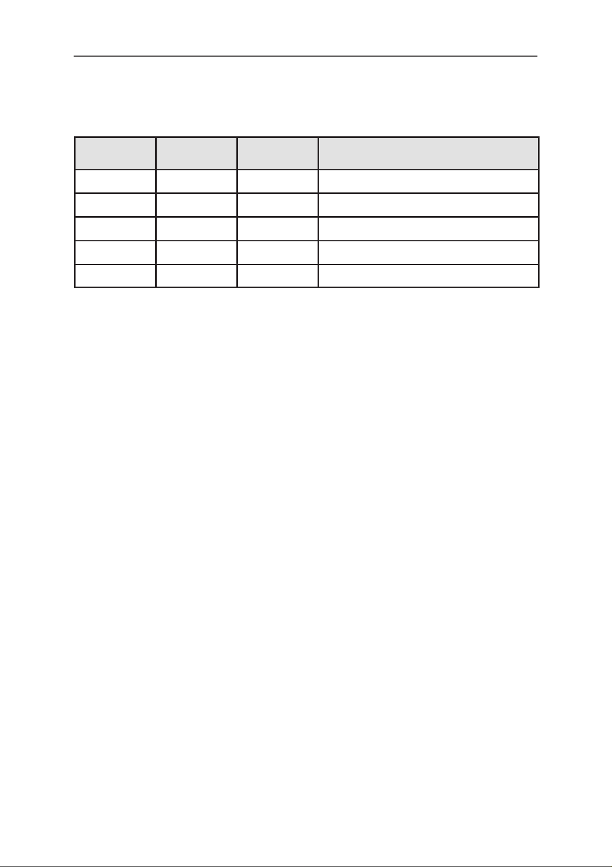
External Signals and Connections
The HSE–6XA has an 8–pin connector for connection to the junction box,
system cable and transceiver via coiled cord.
Issue2 02/00
Page 5 – 5
Page 6
NME–2A
P.A.M.S.
Handset HSE - 6XA
RXD
HANDSET
47R
47R
1k
100k
10uF
47nF
HJ
Technical Documentation
VBS
DGND
M2BUS
N/C
PWR
AGND
MIC
EAR
Figure 1. Handset connector
Signal names and basic interface connections:
Pin Name Level Comments
1 VBS typ. 13.2 V
min. 10.0 V
max. 17.0 V
2 DGND Digital ground
3 MBUS Input: ”0”< 0.9 V Input levels at processor
”1”> 1.9 V input/RxD
Output: ”0”< 0.5 V Max allowed capacitance 2
nF
4 No connection
5 POWER Series diode dropout 0.7 V
6 AGND Analog ground
7 MIC max. 2 V
rms
8 EAR max. 1.2 V
rms
No DC connection
DC 0.0 V
Display Specifications
The HSE–6XA comprises a 16 character (5x2) dot matrix and two and a
half seven segment indexes.
The HSE–6XA comprises a 2x8 (5x7) dot matrix display for 2
seven–segment characters, a signal strength indicator (left bar) and a
number of fixed indicators over and under the character lines.
Page 5 – 6
Issue2 02/00
Page 7

P.A.M.S.
NME–2A
Technical Documentation
The yellow–green supertwist liquid crystal display is connected to the pcb
by means of elastomer connectors. The display is illuminated with green
LEDs from both sides.
Technical specifications for the display include:
Display type Yellow–green supertwist lcd, transflective
Illumination colour Yellow–green LED
Driving mode MUX 1:16, 1/5–bias
Driving voltage 7.5 V at +25°C
Temp. compensation 30 mV/°C
Lens thickness 1.1 mm
Display driver NEC µPD7228AG
Storage temperature –30...+85°C
Handset HSE - 6XA
Oper. temperature –25...+70°C
Humidity typ. 50% RH max. 90% RH
Response times t(
Functional Description
Functional Blocks
HSE–6XA Handset consists of the following functional blocks:
– Audio circuit
– Microprocessor
– Keyboard matrix
– Keyboard illumination
– Display controller/driver
– Voltage converter
– LCD display
) < 100 ms (+25°C) < 1500 ms (–25°C)
rise
t(
) < 100 ms (+25°C) < 1500 ms (–25°C)
fall
– Display illumination
The Audio circuit consists of the earphone and the microphone and
corresponding amplifiers.
The Microprocessor is a single chip version with internal ROM and RAM.
The microprocessor controls all other blocks.
The Keyboard matrix is connected directly to microprocessor inputs and
outputs.
Issue2 02/00
Page 5 – 7
Page 8

NME–2A
P.A.M.S.
Handset HSE - 6XA
Keyboard illumination is accomplished with LEDs and is switched on, off
or dimmed by the microprocessor.
The Display controller/driver is connected to the microprocessor over a
parallel data line, and contains a display data RAM and character
generator ROM/RAM.
The Voltage converter converts the voltages of +5 V to –5 V and divides
the voltage between +5 V and –5 V to five levels (V1...V5), which are
connected to the display controller/driver.
The LCD display is connected to pcb and display drivers over two
elastomer connectors.
The Display illumination is of the same type as the keyboard illumination.
Technical Documentation
Page 5 – 8
Issue2 02/00
Page 9

P.A.M.S.
NME–2A
Technical Documentation
Circuit Description
General
The user interface of the handset is of the menu type. Alphabetical
characters can be used. A dot matrix display is provided.
Construction
The handset consists of two body halves with a PC board inserted in
between. A coiled cord, a speaker, an earphone and a microphone are
wired to the PC board.
Handset Module
The HSE–6XA handsets consist of the following functional blocks:
1. microphone amplifier
Handset HSE - 6XA
2. earphone amplifier
3. CPU with peripherals
4. Hook indicator
5. M2BUS electronics
6. LCD display
7. display controller/driver
8. keyboard matrix
9. illumination
10. voltage supply
11. power on/off logic
12. oscillators
Microphone Amplifier
The microphone is biased through the RC filter R135,C37,C65 and source
resistor R49.
The frequency response of the microphone is filtered to obtain a suitable
shape by low pass filters C10/R60 and R10/R11/C11/C12/C14/R8 and
high pass filter R9/C13. The amplification is about 29 dB with a 1 kHz
signal. The microphone amplifier is built around OPAMP N3 (pin 5,6,7).
Issue2 02/00
Page 5 – 9
Page 10

NME–2A
P.A.M.S.
Handset HSE - 6XA
Earphone Amplifier
The Earphone amplifier is of the differential type. Total amplification is
about 10 dB. The reference voltage is 4.0 volts. The earphone amplifier is
built around OPAMP N3 (pin 1,2,3 and pin 12,13,14)
CPU with Peripherals
Microprocessor D1 is a single chip version with internal ROM and RAM. It
has 16 kbytes of ROM and 256 bytes of RAM. It controls the other blocks
on the basis of information coming from the M2BUS. In addition, it reads
the user inputs, and sends them to the M2BUS.
HOOK Indicator
On–hook/off–hook information is received from a reed relay, which is
located on the PC board and controlled by a magnet in the handset
cradle.
M2BUS Electronics
Technical Documentation
The MBUS is a serial data bus with which the handset sends messages
to, and receives them from, the radio unit. Transistor V28 sends the
outgoing messages (TXD). Incoming data comes to processor pin 11
(RXD). Net free state is controlled by software before message sending.
LCD Display
The display is a 16 symbol 5 x 7 dot matrix supertwist LCD with two
7–segment characters and a few indicators. The LCD is connected to the
PCB by two elastomer connectors. The multiplexing ratio is 1:16.
Display Controller/Driver
The Display controller/driver is connected to the microprocessor by a
parallel (4 bit) data line, and contains display data RAM and character
generator ROM/RAM. All other characters are created by the processor
ROM. There is reserved a memory location for one character in RAM,
loaded by a M2BUS message.
Resistors R35, R42 and R88 comprise a resistor network from which the
LCD driving voltages are received. The voltage between +5 V and – 5 V is
divided to five levels which are applied to the display driver. R41 provides
temperature compensation (about 10 mV/ °C).
Page 5 – 10
Issue2 02/00
Page 11

P.A.M.S.
NME–2A
Technical Documentation
Keyboard Matrix
Keyboard has a 3 x 8 line matrix. Four of the eight write lines are used in
common with display driver data lines. A diode in each of these lines
prevents any contention in data lines when two or more keys are
depressed at the same time.
Illumination
The keyboard and the display are illuminated by LEDs. They can all be
switched on or off. Furthermore the display LEDs have 3 dimmer levels.
The on/off and dimmer function is controlled by the microprocessor.
Variations in power supply voltage (10.8V to 15.6V) do not affect
illumination as all LEDs are powered by constant current sources.
The keyboard is lit by 22 LEDs. There is one illumination LED for each
button.
The display is lit by six LEDs V9...V14 (three in series). The LEDs are
located on the PC board at the ends of the plastic display light conductor.
The light conductor is beneath the display.
Handset HSE - 6XA
Voltage Supply
The handset receives the battery voltage of the radio unit (about 12 V).
This voltage is fed to the LEDs and the voltage regulators. There is an
eight volt regulator N3 for audio circuits and a five volt regulator, N4, for
the logic.
The analog 8V supply is divided to 4.0 volt by resistors R3 and R4 and
buffered by op.amp. N3 (pin 8,9,10) connected as a voltage follower to get
the reference voltage for the audio amplifiers.
The negative five volt supply for the display driver is created by diode V29
and capacitors C17 and C24. The drive frequency is produced and
buffered by inverter D3.
To avoid audio disturbances, ground potentials are separated between the
analog and digital parts. AGND is the analog ground where the ground
current is almost zero. DGND is the ground for the digital circuits and
circuits which use more power, such as LEDs.
Power on/off Logic
The power on/off switch is located on the keyboard (but not in the matrix).
The radio unit detects the depression of the power button and turns power
on. When the button is pressed while power is on, the microcontroller of
the handset detects it and sends a M2BUS message to the radio unit. The
radio unit detects the duration of the key depression; if it is more than 0.5
seconds it will turn power off.
Issue2 02/00
Page 5 – 11
Page 12

NME–2A
P.A.M.S.
Handset HSE - 6XA
Oscillators
The clock frequency of 7.3728 MHz for the microcontroller is generated by
crystal oscillator B4. In order to decreae harmonic frequencies resistor R2
and capacitor C32 are added.
The oscillator for the display driver and the negative five volt generator
comprises inverter D3, resistors R33 and R34 and capacitor C47. The
frequency is about 200 kHz.
Technical Documentation
Page 5 – 12
Issue2 02/00
Page 13

P.A.M.S.
NME–2A
Technical Documentation
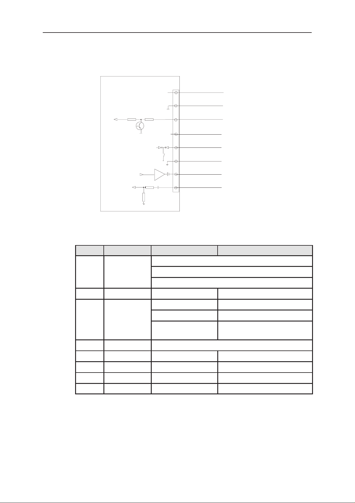
Block Diagram of HSE–6XA
5x7 DOT MATRIX LCD 2x8 CHARACTERS + 2x7– SEGMENT
LCD DRIVER/CONTROLLER NEC uPD7228AG
C(41:0)
CLK
OSCILLATOR
CLK
VDD
GND
DC – CONVERTER
V1
V2
V3
V4
V5
CLK
VDD
GND
VDD
GND
VLC1
VLC2
VLC3
VLC4
VLC5
COLUMN
DRIVER
ROW
DRIVER
DISPLAY
DATARAM
100x8 bit
CHARACTER
GENERATOR
ROM
5600 bit
I/O
BUFFER
DISPLAY
ILLUMINATION
R(15:0)
RESET
CS
C/D
BUSY
STB
DB(3:0)
Handset HSE - 6XA
+12V
DISPILL
DISPDIMM
DISPCTRL
KEYBOARD MATRIX
KEYBOARD
ILLUMINATION
+12V
VDD
LOGIC
5V
EARDR
+12V
KBRDILL
PWR
MBUS
INTERFACE
RESET
BLOCK
AUDIO BLOCK
KBRDILL
KBRDDIMM
RESET
INTEL 87C51FB
8bit microcontroller
ROM 16k
RAM 256b
HOOK
DISPILL
DISPDIMM
HOOK– IND.
AUDIO
8V
4
3
12
MBUS
+12V
DGND
LSP
Issue2 02/00
+8V
PWR
5
7
6
8
POWER
AGND
MIC EAR
Figure 2. Block Diagram – HSE–6XA
D0000111
Page 5 – 13
Page 14

NME–2A
P.A.M.S.
Handset HSE - 6XA
Exploded View of HSE–6XA
Technical Documentation
13
Figure 3. Exploded View HSE–6XA
Assembly Parts
ITEM Q’TY CODE DESCRIPTION VALUE, TYPE
1 9450015 Front cover 1D 21067
2 9450014 Bottom cover 1D 21068
3 Spare part combination
4 9790169 Keypad HSE–6XA DMC 00069
5 9204295 Logo plate ”Nokia” 4D 21063
6 9457035 Display lens 4D 21151
7 7100410 Coil cord 3C 21414
8 6293003 PT–screw FeZn KB 30x14 WN1442
9 9380154 Label Blank
12 9450013 Volume button 2D 21137
13 9480329 Foam Piece
Page 5 – 14
Issue2 02/00
Page 15

P.A.M.S.
NME–2A
Technical Documentation
Handset HSE - 6XA
Parts List of EH9 v.3.4
(EDMS Issue 3.4)
ITEM CODE DESCRIPTION VALUE TYPE
R001 1430087 Chip resistor 100 k 5 % 0.063 W 0603
R002 1430111 Chip resistor 1.0 M 5 % 0.063 W 0603
R003 1430087 Chip resistor 100 k 5 % 0.063 W 0603
R004 1430087 Chip resistor 100 k 5 % 0.063 W 0603
R006 1430075 Chip resistor 33 k 5 % 0.063 W 0603
R007 1430087 Chip resistor 100 k 5 % 0.063 W 0603
R008 1430067 Chip resistor 15 k 5 % 0.063 W 0603
R009 1430017 Chip resistor 390 5 % 0.063 W 0603
R010 1430067 Chip resistor 15 k 5 % 0.063 W 0603
R011 1430067 Chip resistor 15 k 5 % 0.063 W 0603
R012 1430035 Chip resistor 1.0 k 5 % 0.063 W 0603
R013 1430167 Chip resistor 47 5 % 0.063 W 0603
R015 1430065 Chip resistor 10 k 5 % 0.063 W 0603
R018 1430049 Chip resistor 3.9 k 5 % 0.063 W 0603
R019 1430049 Chip resistor 3.9 k 5 % 0.063 W 0603
R021 1430087 Chip resistor 100 k 5 % 0.063 W 0603
R022 1430035 Chip resistor 1.0 k 5 % 0.063 W 0603
R025 1430065 Chip resistor 10 k 5 % 0.063 W 0603
R026 1430065 Chip resistor 10 k 5 % 0.063 W 0603
R027 1430065 Chip resistor 10 k 5 % 0.063 W 0603
R028 1430065 Chip resistor 10 k 5 % 0.063 W 0603
R029 1430057 Chip resistor 8.2 k 5 % 0.063 W 0603
R030 1430049 Chip resistor 3.9 k 5 % 0.063 W 0603
R033 1430087 Chip resistor 100 k 5 % 0.063 W 0603
R034 1430065 Chip resistor 10 k 5 % 0.063 W 0603
R035 1430067 Chip resistor 15 k 5 % 0.063 W 0603
R036 1430067 Chip resistor 15 k 5 % 0.063 W 0603
R037 1430067 Chip resistor 15 k 5 % 0.063 W 0603
R038 1430067 Chip resistor 15 k 5 % 0.063 W 0603
R039 1430067 Chip resistor 15 k 5 % 0.063 W 0603
R040 1430065 Chip resistor 10 k 5 % 0.063 W 0603
R041 1800619 NTC resistor 15 k 10 % 1206
R042 1430049 Chip resistor 3.9 k 5 % 0.063 W 0603
R049 1430043 Chip resistor 2.2 k 5 % 0.063 W 0603
R060 1430067 Chip resistor 15 k 5 % 0.063 W 0603
R063 1430075 Chip resistor 33 k 5 % 0.063 W 0603
R067 1430067 Chip resistor 15 k 5 % 0.063 W 0603
Issue2 02/00
Page 5 – 15
Page 16

NME–2A
P.A.M.S.
Handset HSE - 6XA
R072 1430087 Chip resistor 100 k 5 % 0.063 W 0603
R073 1430075 Chip resistor 33 k 5 % 0.063 W 0603
R074 1430087 Chip resistor 100 k 5 % 0.063 W 0603
R075 1430087 Chip resistor 100 k 5 % 0.063 W 0603
R076 1430075 Chip resistor 33 k 5 % 0.063 W 0603
R077 1430075 Chip resistor 33 k 5 % 0.063 W 0603
R078 1430075 Chip resistor 33 k 5 % 0.063 W 0603
R079 1430065 Chip resistor 10 k 5 % 0.063 W 0603
R088 1430043 Chip resistor 2.2 k 5 % 0.063 W 0603
R104 1430057 Chip resistor 8.2 k 5 % 0.063 W 0603
R105 1430087 Chip resistor 100 k 5 % 0.063 W 0603
R107 1430065 Chip resistor 10 k 5 % 0.063 W 0603
R108 1430065 Chip resistor 10 k 5 % 0.063 W 0603
R109 1430065 Chip resistor 10 k 5 % 0.063 W 0603
R118 1430167 Chip resistor 47 5 % 0.063 W 0603
R120 1430167 Chip resistor 47 5 % 0.063 W 0603
R121 1430167 Chip resistor 47 5 % 0.063 W 0603
R122 1430167 Chip resistor 47 5 % 0.063 W 0603
R123 1430167 Chip resistor 47 5 % 0.063 W 0603
R124 1430151 Chip resistor 10 5 % 0.063 W 0603
R125 1430151 Chip resistor 10 5 % 0.063 W 0603
R128 1430065 Chip resistor 10 k 5 % 0.063 W 0603
R129 1430075 Chip resistor 33 k 5 % 0.063 W 0603
R130 1430065 Chip resistor 10 k 5 % 0.063 W 0603
R131 1430065 Chip resistor 10 k 5 % 0.063 W 0603
R132 1430065 Chip resistor 10 k 5 % 0.063 W 0603
R133 1430049 Chip resistor 3.9 k 5 % 0.063 W 0603
R134 1430035 Chip resistor 1.0 k 5 % 0.063 W 0603
R135 1430035 Chip resistor 1.0 k 5 % 0.063 W 0603
R136 1430035 Chip resistor 1.0 k 5 % 0.063 W 0603
R138 1430167 Chip resistor 47 5 % 0.063 W 0603
R139 1430035 Chip resistor 1.0 k 5 % 0.063 W 0603
R140 1430035 Chip resistor 1.0 k 5 % 0.063 W 0603
C007 2307816 Ceramic cap. 47 n 20 % 25 V 0805
C008 2610005 Tantalum cap. 10 u 20 % 16 V 3.5x2.8x1.9
C009 2604209 Tantalum cap. 1.0 u 20 % 16 V 3.2x1.6x1.6
C010 2610005 Tantalum cap. 10 u 20 % 16 V 3.5x2.8x1.9
C011 2320083 Ceramic cap. 1.0 n 5 % 50 V 0603
C012 2320107 Ceramic cap. 10 n 5 % 50 V 0603
C013 2610005 Tantalum cap. 10 u 20 % 16 V 3.5x2.8x1.9
C014 2320099 Ceramic cap. 4.7 n 5 % 50 V 0603
C015 2307816 Ceramic cap. 47 n 20 % 25 V 0805
Technical Documentation
Page 5 – 16
Issue2 02/00
Page 17

P.A.M.S.
NME–2A
Technical Documentation
C017 2307816 Ceramic cap. 47 n 20 % 25 V 0805
C018 2320107 Ceramic cap. 10 n 5 % 50 V 0603
C019 2307816 Ceramic cap. 47 n 20 % 25 V 0805
C022 2320045 Ceramic cap. 27 p 5 % 50 V 0603
C023 2320045 Ceramic cap. 27 p 5 % 50 V 0603
C024 2307816 Ceramic cap. 47 n 20 % 25 V 0805
C028 2610005 Tantalum cap. 10 u 20 % 16 V 3.5x2.8x1.9
C032 2320035 Ceramic cap. 10 p 5 % 50 V 0603
C033 2604209 Tantalum cap. 1.0 u 20 % 16 V 3.2x1.6x1.6
C034 2307816 Ceramic cap. 47 n 20 % 25 V 0805
C037 2610005 Tantalum cap. 10 u 20 % 16 V 3.5x2.8x1.9
C038 2320059 Ceramic cap. 100 p 5 % 50 V 0603
C039 2320107 Ceramic cap. 10 n 5 % 50 V 0603
C040 2320107 Ceramic cap. 10 n 5 % 50 V 0603
C041 2320107 Ceramic cap. 10 n 5 % 50 V 0603
C042 2320107 Ceramic cap. 10 n 5 % 50 V 0603
C043 2320059 Ceramic cap. 100 p 5 % 50 V 0603
C044 2320059 Ceramic cap. 100 p 5 % 50 V 0603
C045 2320059 Ceramic cap. 100 p 5 % 50 V 0603
C046 2320059 Ceramic cap. 100 p 5 % 50 V 0603
C047 2320059 Ceramic cap. 100 p 5 % 50 V 0603
C048 2320059 Ceramic cap. 100 p 5 % 50 V 0603
C049 2320059 Ceramic cap. 100 p 5 % 50 V 0603
C050 2320059 Ceramic cap. 100 p 5 % 50 V 0603
C051 2320059 Ceramic cap. 100 p 5 % 50 V 0603
C052 2320059 Ceramic cap. 100 p 5 % 50 V 0603
C053 2320059 Ceramic cap. 100 p 5 % 50 V 0603
C054 2320059 Ceramic cap. 100 p 5 % 50 V 0603
C055 2320059 Ceramic cap. 100 p 5 % 50 V 0603
C056 2310752 Ceramic cap. 10 n 20 % 50 V 0805
C057 2307816 Ceramic cap. 47 n 20 % 25 V 0805
C058 2307816 Ceramic cap. 47 n 20 % 25 V 0805
C059 2307816 Ceramic cap. 47 n 20 % 25 V 0805
C060 2307816 Ceramic cap. 47 n 20 % 25 V 0805
C061 2604209 Tantalum cap. 1.0 u 20 % 16 V 3.2x1.6x1.6
C062 2604209 Tantalum cap. 1.0 u 20 % 16 V 3.2x1.6x1.6
C063 2320059 Ceramic cap. 100 p 5 % 50 V 0603
C064 2320099 Ceramic cap. 4.7 n 5 % 50 V 0603
C065 2610005 Tantalum cap. 10 u 20 % 16 V 3.5x2.8x1.9
B004 4510036 Crystal 7.3728 M +–50PPM 12x6x3mm
V001 4864378 Led Green V 0805
V002 4864378 Led Green V 0805
Handset HSE - 6XA
Issue2 02/00
Page 5 – 17
Page 18

NME–2A
P.A.M.S.
Handset HSE - 6XA
V003 4864378 Led Green V 0805
V004 4864378 Led Green V 0805
V005 4864378 Led Green V 0805
V006 4864378 Led Green V 0805
V007 4864378 Led Green V 0805
V008 4864378 Led Green V 0805
V009 4864378 Led Green V 0805
V010 4864378 Led Green V 0805
V011 4864378 Led Green V 0805
V012 4864378 Led Green V 0805
V013 4864378 Led Green V 0805
V014 4864378 Led Green V 0805
V015 4200917 Transistor BC848B/BCW32 npn 30 V 100 mA SOT23
V026 4200917 Transistor BC848B/BCW32 npn 30 V 100 mA SOT23
V027 4200917 Transistor BC848B/BCW32 npn 30 V 100 mA SOT23
V028 4200917 Transistor BC848B/BCW32 npn 30 V 100 mA SOT23
V029 4108639 Diode x 2 BAS28 75 V 250 mA SOT143
V032 4108639 Diode x 2 BAS28 75 V 250 mA SOT143
V033 4108639 Diode x 2 BAS28 75 V 250 mA SOT143
V034 4200917 Transistor BC848B/BCW32 npn 30 V 100 mA SOT23
V035 4200917 Transistor BC848B/BCW32 npn 30 V 100 mA SOT23
V036 4108639 Diode x 2 BAS28 75 V 250 mA SOT143
V037 4200917 Transistor BC848B/BCW32 npn 30 V 100 mA SOT23
V038 4108639 Diode x 2 BAS28 75 V 250 mA SOT143
V039 4200917 Transistor BC848B/BCW32 npn 30 V 100 mA SOT23
V040 4200917 Transistor BC848B/BCW32 npn 30 V 100 mA SOT23
V041 4200917 Transistor BC848B/BCW32 npn 30 V 100 mA SOT23
V042 4200917 Transistor BC848B/BCW32 npn 30 V 100 mA SOT23
V043 4864378 Led Green V 0805
V044 4864378 Led Green V 0805
V045 4864378 Led Green V 0805
V046 4864378 Led Green V 0805
V047 4864378 Led Green V 0805
V048 4864378 Led Green V 0805
V049 4864378 Led Green V 0805
V050 4864378 Led Green V 0805
V051 4864378 Led Green V 0805
V052 4864378 Led Green V 0805
V053 4864378 Led Green V 0805
V054 4864378 Led Green V 0805
V055 4864378 Led Green V 0805
V056 4864378 Led Green V 0805
Technical Documentation
Page 5 – 18
Issue2 02/00
Page 19

P.A.M.S.
NME–2A
Technical Documentation
D001 0240427 MCU Software Module
4370157 MCU 8BIT5V OTP16K RAM256X8 PLCC44
8400472 ROM Code
9380149 Sticker Brady LAT–2–747 9.5X9.5
D002 4309047 IC, LCD driver uPD7228 QFP80
D003 4309569 IC, 6 x inverter 4069 SO14
N003 4306494 IC, 2 x op.amp. TL074ID SO14
N004 4301062 IC, regulator LP2951AC SO8S
N005 4301062 IC, regulator LP2951AC SO8S
S022 5200116 Bush button switch 1–lock 1–pole 1–POLE
S023 5200116 Bush button switch 1–lock 1–pole 1–POLE
S025 5304759 Reed relay 10at 0.5a 2x15 smd
X001 5416638 Connector 8–pole right angle 1.5 1.5
X002 5416640 Pin header m1x2 p1.5 90deg 1a0r02 1A0R02
X003 5416640 Pin header m1x2 p1.5 90deg 1a0r02 1A0R02
X004 5416640 Pin header m1x2 p1.5 90deg 1a0r02 1A0R02
A001 9510038 RF shield 3D21421 HSE–1
P001 9854152 PC board EH9 135.9x48.0x1.6 m4 3/pa
5140450 Cond. microphone 62+– 2DB HSE–1
5140566 Receiver capsule cr–4e with leads LEADS
9854152 PCB EH9 135.9X48.0X1.6 M4 3/PA
Handset HSE - 6XA
Issue2 02/00
Page 5 – 19
Page 20

NME–2A
P.A.M.S.
Handset HSE - 6XA
Technical Documentation
Parts List of EH9 v.4.1
(0200905 EDMS Issue 4.1)
ITEM CODE DESCRIPTION VALUE TYPE
R001 1430087 Chip resistor 100 k 5 % 0.063 W 0603
R002 1430111 Chip resistor 1.0 M 5 % 0.063 W 0603
R003 1430087 Chip resistor 100 k 5 % 0.063 W 0603
R004 1430087 Chip resistor 100 k 5 % 0.063 W 0603
R006 1430075 Chip resistor 33 k 5 % 0.063 W 0603
R007 1430087 Chip resistor 100 k 5 % 0.063 W 0603
R008 1430067 Chip resistor 15 k 5 % 0.063 W 0603
R009 1430017 Chip resistor 390 5 % 0.063 W 0603
R010 1430067 Chip resistor 15 k 5 % 0.063 W 0603
R011 1430067 Chip resistor 15 k 5 % 0.063 W 0603
R012 1430035 Chip resistor 1.0 k 5 % 0.063 W 0603
R013 1430167 Chip resistor 47 5 % 0.063 W 0603
R014 1430001 Chip resistor 100 5 % 0.063 W 0603
R015 1430065 Chip resistor 10 k 5 % 0.063 W 0603
R016 1430007 Chip resistor 180 5 % 0.063 W 0603
R017 1430007 Chip resistor 180 5 % 0.063 W 0603
R018 1430049 Chip resistor 3.9 k 5 % 0.063 W 0603
R019 1430049 Chip resistor 3.9 k 5 % 0.063 W 0603
R021 1430087 Chip resistor 100 k 5 % 0.063 W 0603
R022 1430035 Chip resistor 1.0 k 5 % 0.063 W 0603
R023 1430001 Chip resistor 100 5 % 0.063 W 0603
R025 1430065 Chip resistor 10 k 5 % 0.063 W 0603
R026 1430065 Chip resistor 10 k 5 % 0.063 W 0603
R027 1430065 Chip resistor 10 k 5 % 0.063 W 0603
R028 1430065 Chip resistor 10 k 5 % 0.063 W 0603
R029 1430057 Chip resistor 8.2 k 5 % 0.063 W 0603
R030 1430049 Chip resistor 3.9 k 5 % 0.063 W 0603
R033 1430087 Chip resistor 100 k 5 % 0.063 W 0603
R034 1430065 Chip resistor 10 k 5 % 0.063 W 0603
R035 1430067 Chip resistor 15 k 5 % 0.063 W 0603
R036 1430067 Chip resistor 15 k 5 % 0.063 W 0603
R037 1430067 Chip resistor 15 k 5 % 0.063 W 0603
R038 1430067 Chip resistor 15 k 5 % 0.063 W 0603
R039 1430067 Chip resistor 15 k 5 % 0.063 W 0603
R040 1430065 Chip resistor 10 k 5 % 0.063 W 0603
R041 1800619 NTC resistor 15 k 10 % 1206
R042 1430049 Chip resistor 3.9 k 5 % 0.063 W 0603
R049 1430043 Chip resistor 2.2 k 5 % 0.063 W 0603
R060 1430067 Chip resistor 15 k 5 % 0.063 W 0603
R063 1430075 Chip resistor 33 k 5 % 0.063 W 0603
R067 1430067 Chip resistor 15 k 5 % 0.063 W 0603
R071 1430001 Chip resistor 100 5 % 0.063 W 0603
Page 5 – 20
Issue2 02/00
Page 21

P.A.M.S.
NME–2A
Technical Documentation
R072 1430087 Chip resistor 100 k 5 % 0.063 W 0603
R073 1430075 Chip resistor 33 k 5 % 0.063 W 0603
R074 1430087 Chip resistor 100 k 5 % 0.063 W 0603
R075 1430087 Chip resistor 100 k 5 % 0.063 W 0603
R076 1430075 Chip resistor 33 k 5 % 0.063 W 0603
R077 1430075 Chip resistor 33 k 5 % 0.063 W 0603
R078 1430075 Chip resistor 33 k 5 % 0.063 W 0603
R079 1430065 Chip resistor 10 k 5 % 0.063 W 0603
R081 1430007 Chip resistor 180 5 % 0.063 W 0603
R082 1430007 Chip resistor 180 5 % 0.063 W 0603
R083 1430007 Chip resistor 180 5 % 0.063 W 0603
R084 1430007 Chip resistor 180 5 % 0.063 W 0603
R088 1430043 Chip resistor 2.2 k 5 % 0.063 W 0603
R103 1430001 Chip resistor 100 5 % 0.063 W 0603
R104 1430057 Chip resistor 8.2 k 5 % 0.063 W 0603
R105 1430087 Chip resistor 100 k 5 % 0.063 W 0603
R107 1430065 Chip resistor 10 k 5 % 0.063 W 0603
R108 1430065 Chip resistor 10 k 5 % 0.063 W 0603
R109 1430065 Chip resistor 10 k 5 % 0.063 W 0603
R118 1430167 Chip resistor 47 5 % 0.063 W 0603
R119 1430007 Chip resistor 180 5 % 0.063 W 0603
R120 1430167 Chip resistor 47 5 % 0.063 W 0603
R121 1430167 Chip resistor 47 5 % 0.063 W 0603
R122 1430167 Chip resistor 47 5 % 0.063 W 0603
R123 1430167 Chip resistor 47 5 % 0.063 W 0603
R124 1430151 Chip resistor 10 5 % 0.1 W 0603
R125 1430151 Chip resistor 10 5 % 0.1 W 0603
R128 1430065 Chip resistor 10 k 5 % 0.063 W 0603
R129 1430075 Chip resistor 33 k 5 % 0.063 W 0603
R130 1430065 Chip resistor 10 k 5 % 0.063 W 0603
R131 1430065 Chip resistor 10 k 5 % 0.063 W 0603
R132 1430065 Chip resistor 10 k 5 % 0.063 W 0603
R133 1430049 Chip resistor 3.9 k 5 % 0.063 W 0603
R134 1430035 Chip resistor 1.0 k 5 % 0.063 W 0603
R135 1430035 Chip resistor 1.0 k 5 % 0.063 W 0603
R136 1430035 Chip resistor 1.0 k 5 % 0.063 W 0603
R137 1430001 Chip resistor 100 5 % 0.063 W 0603
R138 1430167 Chip resistor 47 5 % 0.063 W 0603
R139 1430035 Chip resistor 1.0 k 5 % 0.063 W 0603
R140 1430035 Chip resistor 1.0 k 5 % 0.063 W 0603
C007 2307816 Ceramic cap. 47 n 20 % 25 V 0805
C008 2610005 Tantalum cap. 10 u 20 % 16 V
3.5x2.8x1.9
C009 2604209 Tantalum cap. 1.0 u 20 % 16 V
3.2x1.6x1.6
C010 2610005 Tantalum cap. 10 u 20 % 16 V
3.5x2.8x1.9
Handset HSE - 6XA
Issue2 02/00
Page 5 – 21
Page 22

NME–2A
P.A.M.S.
Handset HSE - 6XA
C011 2320083 Ceramic cap. 1.0 n 5 % 50 V 0603
C012 2320107 Ceramic cap. 10 n 5 % 50 V 0603
C013 2610005 Tantalum cap. 10 u 20 % 16 V
3.5x2.8x1.9
C014 2320099 Ceramic cap. 4.7 n 5 % 50 V 0603
C015 2307816 Ceramic cap. 47 n 20 % 25 V 0805
C017 2307816 Ceramic cap. 47 n 20 % 25 V 0805
C018 2320107 Ceramic cap. 10 n 5 % 50 V 0603
C019 2307816 Ceramic cap. 47 n 20 % 25 V 0805
C022 2320045 Ceramic cap. 27 p 5 % 50 V 0603
C023 2320045 Ceramic cap. 27 p 5 % 50 V 0603
C024 2307816 Ceramic cap. 47 n 20 % 25 V 0805
C028 2610005 Tantalum cap. 10 u 20 % 16 V
3.5x2.8x1.9
C032 2320035 Ceramic cap. 10 p 5 % 50 V 0603
C033 2604209 Tantalum cap. 1.0 u 20 % 16 V
3.2x1.6x1.6
C034 2307816 Ceramic cap. 47 n 20 % 25 V 0805
C037 2610005 Tantalum cap. 10 u 20 % 16 V
3.5x2.8x1.9
C038 2320059 Ceramic cap. 100 p 5 % 50 V 0603
C039 2320107 Ceramic cap. 10 n 5 % 50 V 0603
C040 2320107 Ceramic cap. 10 n 5 % 50 V 0603
C041 2320107 Ceramic cap. 10 n 5 % 50 V 0603
C042 2320107 Ceramic cap. 10 n 5 % 50 V 0603
C043 2320059 Ceramic cap. 100 p 5 % 50 V 0603
C044 2320059 Ceramic cap. 100 p 5 % 50 V 0603
C045 2320059 Ceramic cap. 100 p 5 % 50 V 0603
C046 2320059 Ceramic cap. 100 p 5 % 50 V 0603
C047 2320059 Ceramic cap. 100 p 5 % 50 V 0603
C048 2320059 Ceramic cap. 100 p 5 % 50 V 0603
C049 2320059 Ceramic cap. 100 p 5 % 50 V 0603
C050 2320059 Ceramic cap. 100 p 5 % 50 V 0603
C051 2320059 Ceramic cap. 100 p 5 % 50 V 0603
C052 2320059 Ceramic cap. 100 p 5 % 50 V 0603
C053 2320059 Ceramic cap. 100 p 5 % 50 V 0603
C054 2320059 Ceramic cap. 100 p 5 % 50 V 0603
C055 2320059 Ceramic cap. 100 p 5 % 50 V 0603
C056 2310752 Ceramic cap. 10 n 20 % 50 V 0805
C057 2307816 Ceramic cap. 47 n 20 % 25 V 0805
C058 2307816 Ceramic cap. 47 n 20 % 25 V 0805
C059 2307816 Ceramic cap. 47 n 20 % 25 V 0805
C060 2307816 Ceramic cap. 47 n 20 % 25 V 0805
C061 2604209 Tantalum cap. 1.0 u 20 % 16 V
3.2x1.6x1.6
C062 2604209 Tantalum cap. 1.0 u 20 % 16 V
3.2x1.6x1.6
Technical Documentation
Page 5 – 22
Issue2 02/00
Page 23

P.A.M.S.
NME–2A
Technical Documentation
C063 2320059 Ceramic cap. 100 p 5 % 50 V 0603
C064 2320099 Ceramic cap. 4.7 n 5 % 50 V 0603
C065 2610005 Tantalum cap. 10 u 20 % 16 V
3.5x2.8x1.9
B004 4510036 Crystal 7.3728 M +–50PPM 12x6x3mm
V001 4864378 Led Green V 0805
V002 4864378 Led Green V 0805
V003 4864378 Led Green V 0805
V004 4864378 Led Green V 0805
V005 4864378 Led Green V 0805
V006 4864378 Led Green V 0805
V007 4864378 Led Green V 0805
V008 4864378 Led Green V 0805
V009 4864378 Led Green V 0805
V010 4864378 Led Green V 0805
V011 4864378 Led Green V 0805
V012 4864378 Led Green V 0805
V013 4864378 Led Green V 0805
V014 4864378 Led Green V 0805
V015 4200917 Transistor BC848B/BCW32 npn 30 V 100 mA
SOT23
V026 4200917 Transistor BC848B/BCW32 npn 30 V 100 mA
SOT23
V027 4200917 Transistor BC848B/BCW32 npn 30 V 100 mA
SOT23
V028 4200917 Transistor BC848B/BCW32 npn 30 V 100 mA
SOT23
V029 4108639 Diode x 2 BAS28 75 V 250 mA
SOT143
V032 4108639 Diode x 2 BAS28 75 V 250 mA
SOT143
V033 4108639 Diode x 2 BAS28 75 V 250 mA
SOT143
V034 4200917 Transistor BC848B/BCW32 npn 30 V 100 mA
SOT23
V035 4200917 Transistor BC848B/BCW32 npn 30 V 100 mA
SOT23
V036 4108639 Diode x 2 BAS28 75 V 250 mA
SOT143
V037 4200917 Transistor BC848B/BCW32 npn 30 V 100 mA
SOT23
V038 4108639 Diode x 2 BAS28 75 V 250 mA
SOT143
V039 4200917 Transistor BC848B/BCW32 npn 30 V 100 mA
SOT23
V040 4200917 Transistor BC848B/BCW32 npn 30 V 100 mA
SOT23
Handset HSE - 6XA
Issue2 02/00
Page 5 – 23
Page 24

NME–2A
P.A.M.S.
Handset HSE - 6XA
V041 4200917 Transistor BC848B/BCW32 npn30V100mSOT23
V042 4200917 Transistor BC848B/BCW32 npn30V100mSOT23
V043 4864378 Led Green V 0805
V044 4864378 Led Green V 0805
V045 4864378 Led Green V 0805
V046 4864378 Led Green V 0805
V047 4864378 Led Green V 0805
V048 4864378 Led Green V 0805
V049 4864378 Led Green V 0805
V050 4864378 Led Green V 0805
V051 4864378 Led Green V 0805
V052 4864378 Led Green V 0805
V053 4864378 Led Green V 0805
V054 4864378 Led Green V 0805
V055 4864378 Led Green V 0805
V056 4864378 Led Green V 0805
D001 4370437 IC, MCU PLCC44
D002 4309047 IC, LCD driver uPD7228 QFP80
D003 4309569 IC, 6 x inverter 4069 SO14
N003 4306494 IC, 2 x op.amp. TL074ID SO14
N004 4301062 IC, regulator LP2951AC SO8S
N005 4301062 IC, regulator LP2951AC SO8S
S022 5200116 Bush button switch 1–lock 1–POLE
S023 5200116 Bush button switch 1–lock 1–POLE
S025 5304759 Reed relay 10at 0.5a 2x15 smd
X001 5416638 Connector 8–pole right angle 1.5
X002 5416640 Pin header m1x2 p1.5 90deg 1a0r02 1A0R02
X003 5416640 Pin header m1x2 p1.5 90deg 1a0r02 1A0R02
A001 9510038 RF shield 3D21421 HSE–1
P001 9854152 PC board EH9 135.9x48.0x1.6 m4 3/pa
Technical Documentation
Page 5 – 24
Issue2 02/00
 Loading...