

Page 1

Nokia Customer Care
8 — System Module
Issue 1 COMPANY CONFIDENTIAL Page 8 –1
Copyright © 2006 Nokia. All rights reserved.
Page 2
RM-88
Nokia Customer Care System Module
(This page left intentionally blank.)
Page 8 –2 COMPANY CONFIDENTIAL Issue 1
Copyright © 2006 Nokia. All rights reserved.
Page 3
RM-88
System Module Nokia Customer Care
Table of Contents
Baseband description............................................................................................................................................8–5
System module block diagram........................................................................................................................8–5
Baseband functional description.....................................................................................................................8–6
Absolute maximum ratings..............................................................................................................................8–6
Phone modes of operation...............................................................................................................................8–7
Operation modes...............................................................................................................................................8–8
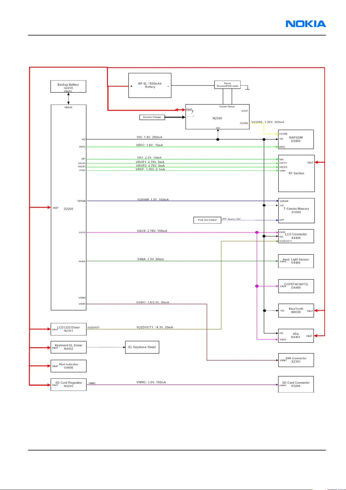
Power distribution............................................................................................................................................8–9
Clocking scheme..............................................................................................................................................8–10
Bluetooth.........................................................................................................................................................8–10
IrDA...................................................................................................................................................................8–11
USB....................................................................................................................................................................8–11
SIM card............................................................................................................................................................8–11
RF-BB interface................................................................................................................................................8–11
FBUS..................................................................................................................................................................8–12
ACI interface.....................................................................................................................................................8–12
SIM interface....................................................................................................................................................8–13
MiniSD interface...............................................................................................................................................8–13
Battery interface..............................................................................................................................................8–14
User interface..................................................................................................................................................8–15
Display interface.........................................................................................................................................8–15
Keyboard.....................................................................................................................................................8–15
Display and keyboard backlight...............................................................................................................8–15
ALS interface...............................................................................................................................................8–15
E-Mail LED....................................................................................................................................................8–16
Audio concept.......................................................................................................................................................8–17
Audio HW architecture....................................................................................................................................8–17
Internal microphone.......................................................................................................................................8–18
Internal earpiece.............................................................................................................................................8–19
Internal speaker..............................................................................................................................................8–19
Vibra circuitry..................................................................................................................................................8–19
Baseband technical specifications......................................................................................................................8–20
External interfaces..........................................................................................................................................8–20
USB IF electrical characteristics......................................................................................................................8–20
FBUS interface electrical characteristics (between RAP and N2300).........................................................8–21
SIM IF connections...........................................................................................................................................8–21
MiniSD interface connections.........................................................................................................................8–22
Charger connector and charging interface connections & electrical characteristics...............................8–23
Battery interface electrical characteristics...................................................................................................8–24
Internal interfaces...........................................................................................................................................8–24
l2C.....................................................................................................................................................................8–24
Keyboard interface electrical characteristics................................................................................................8–24
Display connector and interface connections..............................................................................................8–25
Back-up battery interface electrical characteristics.....................................................................................8–26
Frequency mappings............................................................................................................................................8–27
GSM850 frequencies........................................................................................................................................8–27
EGSM900 frequencies......................................................................................................................................8–28
GSM1800 frequencies......................................................................................................................................8–29
GSM1900 frequencies......................................................................................................................................8–30
Issue 1 COMPANY CONFIDENTIAL Page 8 –3
Copyright © 2006 Nokia. All rights reserved.
Page 4

RM-88
Nokia Customer Care System Module
List of Tables
Table 14 Battery interface connections.............................................................................................................8–15
Table 15 ALS resistor values................................................................................................................................8–16
Table 16 Charging interface connections..........................................................................................................8–23
Table 17 Charging IF electrical characteristics..................................................................................................8–23
Table 18 Battery IF electrical characteristics.....................................................................................................8–24
Table 19 Back-up battery connections...............................................................................................................8–26
Table 20 Back-up battery electrical characteristics..........................................................................................8–26
List of Figures
Figure 52 System level block diagram..................................................................................................................8–6
Figure 53 Power distribution diagram.................................................................................................................8–9
Figure 54 BT-RAP connection..............................................................................................................................8–11
Figure 55 MiniSD contact area & pin order........................................................................................................8–14
Figure 56 Battery pin order.................................................................................................................................8–15
Figure 57 ALS HW implementation.....................................................................................................................8–16
Figure 58 E-mail LED implementation................................................................................................................8–17
Figure 59 Audio block diagram...........................................................................................................................8–18
Figure 60 Internal microphone passive circuitry..............................................................................................8–18
Figure 61 Internal earpiece circuitry..................................................................................................................8–19
Figure 62 Internal speaker circuitry...................................................................................................................8–19
Figure 63 Vibra circuitry......................................................................................................................................8–20
Figure 64 Charger connector...............................................................................................................................8–23
Page 8 –4 COMPANY CONFIDENTIAL Issue 1
Copyright © 2006 Nokia. All rights reserved.
Page 5
RM-88
System Module Nokia Customer Care
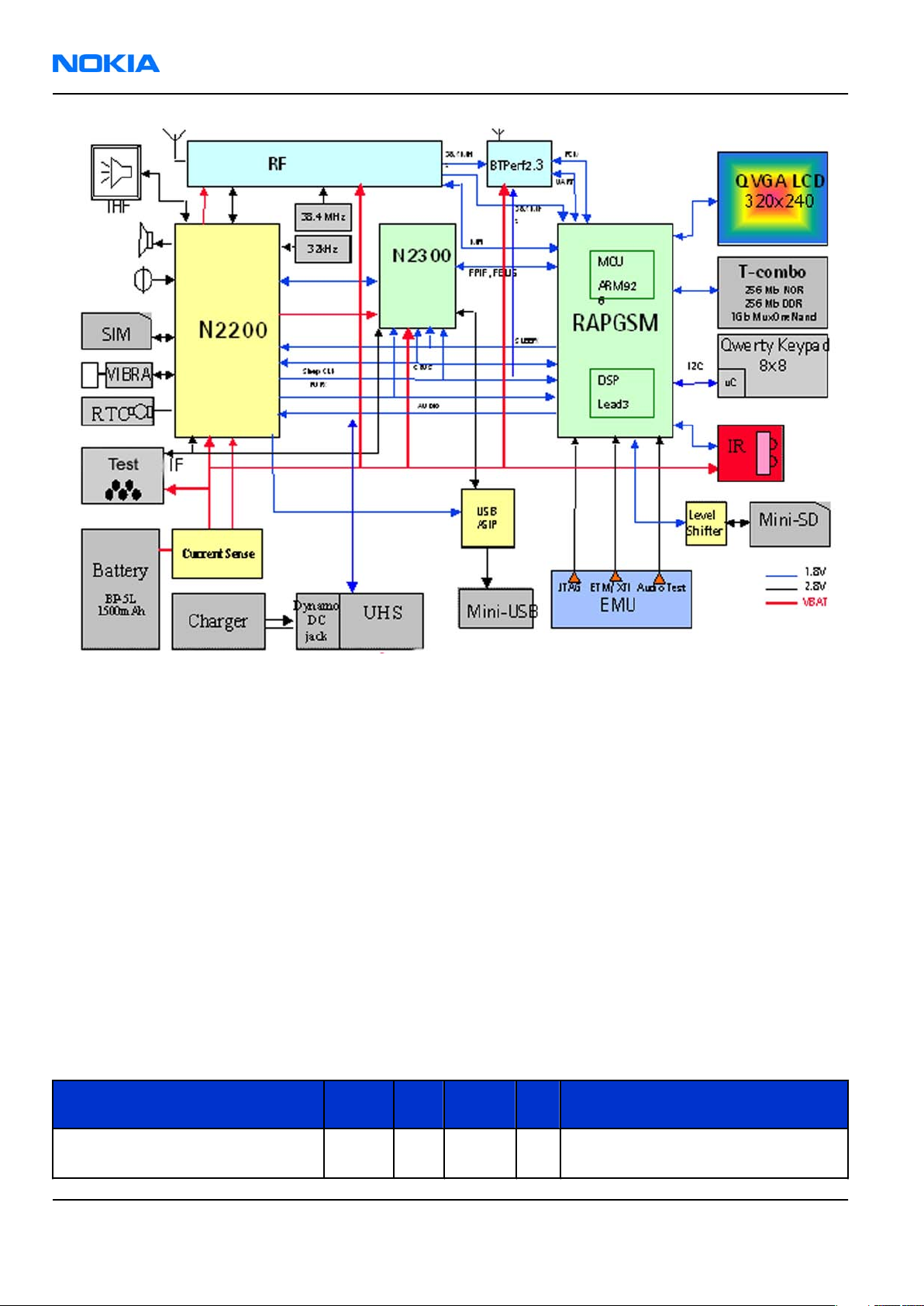
Baseband description
System module block diagram
The device is a quad-band GSM mono-block product with full QWERTY keyboard. It is based on Series 60 UI
Style on the Symbian Operating System (SOS) release (version 9.1).
The device has two antennas; Internal antenna for cellular quad band GSM and BT antenna.
Bluetooth module has its own antenna. System calculations assume 15dB antenna isolation between
Bluetooth and cellular GSM antenna.
Architecture overview
The device is a monoblock quadband GSM/EDGE 850/900/1800/1900 handportable phone running on
Symbian series 60 release 3.0.
Product segment is a Smart phone.
The device baseband is single processor architecture based on CeMEnt G3.1S engine (CeBBo1GSM BB + Ritsa
4.5 RF).
The baseband includes following HW-blocks:
• RAP, GSM EDGE BaseBand ASIC (ARM926EJ-S MCU, Lead3 PH3 DSP)
• N2200 , primary Energy Management ASIC
• N2300, secondary Energy Management ASIC
• T-combo memory, 256Mbit NOR FLASH + 256Mbit DDR-SDRAM + 1Gbit Mux-one Nand combo memory
• Audio (Microphone, Speaker, IHF and external audio)
• EL keyboard backlightning
• Ambient light sensor
• Bottom Connectors (Mini USB-B + 2.5mm Headset Jack + Dynamo DC jack)
• SIM Interface
• BB-RF Interface
• Bluetooth BTPerf 2.3 (BT 2.0 + EDR)
• UI (Oxford QVGA LCD, QWERTY keyboard)
• IR Interface (IrDA, 115.2kbit/s)
• Mini SD Interface (hot swappable)
RF block includes:
• N7505 AHNE RF ASIC (Quad-band GSM functionality based on Ritsa 4.5 engine.)
• N7520 front end module (PA and antenna switch)
• G7500 VCO and G7501 VCXO (38.4MHz)
Issue 1 COMPANY CONFIDENTIAL Page 8 –5
Copyright © 2006 Nokia. All rights reserved.
Page 6
RM-88
Nokia Customer Care System Module
Figure 52 System level block diagram
Baseband functional description
Digital baseband is single processor architecture. It consists of RAP, EM ASIC (N2200), EM ASIC (N2300) and
memories as the core. RAP is a GSM EDGE chip with lots of peripheral features. Supported cellular protocols
in RAP are GSM (minimum EDGE class 10, GPRS phase2). In general RAP consists of three separate parts. The
first part is processor subsystem (PSS) that includes both MCU and DSP processors and related functions. The
second part is MCU peripherals that are peripherals mainly controlled by MCU. The third one is DSP peripherals
that are peripherals mainly controlled by DSP. N2200 is an audio ASIC including also energy management
(EM) functions. With second EM ASIC N2300, it covers the analog audio and energy management function.
N2200 is also the device that handles the power-up and power-down routines of the system. During the
times when the digital BB is alive N2200 handles a variety of tasks that can not be accomplished elsewhere
due to voltage requirements, noise etc. N2300 power IC is intended for energy management control, supply
voltage generation and charge control of mobile phone. N2300 has a step down type (buck) programmable
switch mode regulator for digital core supply generation, up (boost) switch mode regulator with current
control for led supply, charge control circuitry with integrated switch, level shifters and regulator for FBUS/
USB-OTG, and digital circuitry including registers. Stacked triple combo memory (RAM, Nor, Nand in one
package) includes 256Mbit DDR SDRAM , 256Mbit NOR Flash and 1Gbit Mux-One Nand.
Absolute maximum ratings
Signal Min Nom Max
Uni
t
Notes
Battery voltage (idle) -0.3 5.2 V Battery voltage maximum value is
specified during charging is active
Page 8 –6 COMPANY CONFIDENTIAL Issue 1
Copyright © 2006 Nokia. All rights reserved.
Page 7
RM-88
System Module Nokia Customer Care
Signal Min Nom Max
Battery voltage (Call) +3.2 +4.8 V Battery voltage maximum value is
Charger input voltage -0.3 +16 V
Uni
t
specified during charging is active
Notes
Phone modes of operation
Mode Description
NO_SUPPLY (dead) mode means that the main battery is not present or its voltage is too low (below
N2200 master reset threshold) and that the back-up battery voltage is too low.
BACK_UP The main battery is not present or its voltage is too low but back-up battery voltage is
adequate and the 32 kHz oscillator is running (RTC is on).
PWR_OFF In this mode (warm), the main battery is present and its voltage is over N2200 master
reset threshold. All regulators are disabled, PurX is on low state, the RTC is on and the
oscillator is on. PWR_OFF (cold) mode is almost the same as PWR_OFF (warm), but the
RTC and the oscillator are off.
RESET RESET mode is a synonym for start-up sequence. In this mode certain regulators are
enabled and after they and RFClk have stabilized, the system reset (PurX) is released
and PWR_ON mode entered. RESET mode uses 32 kHz clock to count the REST mode
delay (typically 16 ms).
DEEP SLEEP Deep sleep mode is entered only from Pwr_on mode with the aid of sw when the
system's activity is low. At deep sleep, VCTCXO is powering off. System is running with
the sleep clock. Regulators are in sleep mode.
FLASHING FLASHING mode is for SW downloading.
Voltage limits
Parameter Description Value
Master reset
threshold
VMSTR
VMSTR+
VMSTR-
VCOFF+
(N2200) 2.2V (typ.)
Master reset
threshold
level, rising
(N2300) 2.1V (typ.)
Master reset
threshold
level, falling
(N2300) 1.9V (typ.)
Hardware
cutoff
(rising) 2.9V (typ.)
Issue 1 COMPANY CONFIDENTIAL Page 8 –7
Copyright © 2006 Nokia. All rights reserved.
Page 8
RM-88
Nokia Customer Care System Module
Parameter Description Value
Hardware
cutoff
VCOFF-
SWCOFF
The master reset threshold controls the internal reset of N2200 / (N2300). If battery voltage is above VMSTR,
N2300’s charging control logic is alive. Also, RTC is active and supplied from the main battery. Above VMSTR,
N2300 allows the system to be powered on although this may not succeed due to voltage drops during start
up. SW can also consider battery voltage too low for operation and power down the system.
(falling) 2.6V (typ.)
SW cutoff
limit ~3.2V
Power key
The system boots up when power key is pressed (adequate battery voltage, VBAT, present).
Power down can be initiated by pressing the power key again (the system is powered down with the aid of
SW).
Operation modes
There are four different power up possibilities to switch power on:
• Power key is pressed
• Charger is connected
• A pulse is supplied to MBUS line (Clk)
• Internal power up with Real Time Clock alarm.
Power is not switched on by supplying battery voltage as in DCT4 generations
It should be noted that system behavior depends on the type of device the engine is in. The difference is
mainly in the power key concept, basically:
• The power key controls the system power ON/OFF
• The system boots up always when not empty battery is connected. The power key controls only the CMT
functionality. PDA functions are always available
• To the EM ASIC's functionality there is no difference how the power key is connected (the power up and
down signaling and timings are the same)
Page 8 –8 COMPANY CONFIDENTIAL Issue 1
Copyright © 2006 Nokia. All rights reserved.
Page 9
RM-88
System Module Nokia Customer Care
Power distribution
Figure 53 Power distribution diagram
System power-up
Power up procedure starts when the user presses power key (option 1) or when (not empty) battery is
attached (option 2). In addition, some other triggers may start the system.
Issue 1 COMPANY CONFIDENTIAL Page 8 –9
Copyright © 2006 Nokia. All rights reserved.
Page 10

RM-88
Nokia Customer Care System Module
Power down procedure
Controlled powering off is done with the aid of SW when the user requests it or when the battery voltage is
falling too low. Uncontrolled powering off happens for example when battery is suddenly removed.
Clocking scheme
The main system clock is a small signal sine wave created in the RF-section of the engine with Voltage
Controlled, Temperature Compensated, crystal oscillator (VCTCXO). The delivered frequency is 38.4MHz . RAP
has its own sleep mode in which use low accuracy, low frequency sleep clock instead of RF clock. In deep
sleep, ASIC is sleep mode and therefore VCTCXO can be switched off (VCTCXO is a significant power consumer).
In deep sleep also the core voltage is decreased.
Bluetooth
The device uses BTH Perf2.3 solution. The Bluetooth is V 2.0 + EDR. The Bluetooth module is implemented by
using CSR’s BC4-ROM. BlueCore-4 ROM is a single chip radio and baseband IC for Bluetooth 2.4 GHz systems.
In BB5.0 ,BT interface has been designed so that it allows attaching BT modules from different vendors. The
interface consists of UART interface and PCM interface for audio.
Page 8 –10 COMPANY CONFIDENTIAL Issue 1
Copyright © 2006 Nokia. All rights reserved.
Page 11

RM-88
System Module Nokia Customer Care
Figure 54 BT-RAP connection
IrDA
IrDA specifies a reliable, fully digital peer-to-peer data link between IrDA units at data rates from 9600 bits/
s to 115 kbit/s. The link is based on the serial transmission of data as pulses of infra red light at the wave
length of 870nm and angles of +-15degrees at the range 0 - 50 to 100 cm. The transmission is not
omnidirectional but focused and only reaches a peer at a limited line-of-sight distance from the transmitter
thus not disturbing any other units in the neighbourhood.
IR communication is half-duplex e.g. the IR receiver sees its own transmission, and the IR interface is either
transmitting or receiving, but not both at once.
USB
USB (Universal Serial Bus) provides a wired connectivity between a USB host PC and peripheral devices.
USB is a differential serial bus for USB devices. USB controller supports USB specification revision 2.0 with full
speed USB (12 Mbps). The device is connected to the USB host through the system connector. The USB bus is
hot plugged capable, which means that USB devices may be plugged in/out at any time.
SIM card
The device SIM interface supports both1.8V and 3V technology smart cards.
The power is not allowed to be supplied to cards until the power contacts to battery are properly connected.
RF-BB interface
In BB-RF interface there are 19 signal pins between RAP and cellular RF.
Issue 1 COMPANY CONFIDENTIAL Page 8 –11
Copyright © 2006 Nokia. All rights reserved.
Page 12

RM-88
Nokia Customer Care System Module
Between EM (N2200) and cellular RF there are 8 pins + VBAT. RF is controlled directly by RAP and N2200. Digital
control signals, such as RFBus and reset signals, are taken from RAP and analog control signals, such as AFC
and TxC, are taken from EM ASIC (N2200).
RFBUS is similar control bus than CBUS and DBUS, but it is only used as controlling interface between RF and
BaseBand (RAP). RAP controls AFC and TxC signals via TxCData bus and RF regulator control is done via CBUS.
Analog Rx and Tx signals are connected to/from RAP that includes RF converters for this purpose. The TxC
serial bus interface is a one-way bus, which is used to transfer data from RAP3G to the N2200 ASIC TXC DACs.
These DACs are used to control the RF power amplifiers. The TXC bus includes TxCCtrl pin, which is used to
select the EM ASIC (N2200) DAC, the data is written to. In case the TxCCtrl is in low state, the data is written
to the DAC1 and in case the TxCCtrl is in high state, the data is written to DAC2.
The TxC bus clock frequency is programmable but the frequency to be used in CeBBo1 is 19.2 MHz and for
RFBUS the frequency used is 9.6 MHz.
FBUS
USB and FBUS have multiplexed interface between EM ASIC (2300) and RAP.
ACI interface
The ACI (Accessory Control Interface) is a point-to-point, bi-directional, single line serial bus.
It has two main features: the insertion and removal detection of an accessory device and acting as a data
bus between phone and accessory, intended for control purposes. A third function of ACI is to identify and
authenticate the accessory.
Page 8 –12 COMPANY CONFIDENTIAL Issue 1
Copyright © 2006 Nokia. All rights reserved.
Page 13

RM-88
System Module Nokia Customer Care
SIM interface
The device has one SIM (Subscriber Identification Module) interface. It is only accessible if battery is removed.
The SIM interface consists of an internal interface between RAP and EM ASIC (N2200), and of an external
interface between N2200 and SIM contacts.
The EM ASIC SIM1 interface supports both 1.8 V and 3.0 V SIM cards. The SIM interface voltage is first 1.8 V
when the SIM card is inserted, and if the card does not response to the ATR a 3 V interface voltage is used.
MiniSD interface
In the RAP the MMC/SD interface is multiplexed with NAND Flash and SIM2 interfaces.
Issue 1 COMPANY CONFIDENTIAL Page 8 –13
Copyright © 2006 Nokia. All rights reserved.
Page 14
RM-88
Nokia Customer Care System Module
Figure 55 MiniSD contact area & pin order
Battery interface
The battery interface supports a 3-pole battery interface. The interface consists of three connectors: VBAT,
BSI and GND.
The BSI line is used to recognize the battery capacity by a battery internal pull down resistor.
Page 8 –14 COMPANY CONFIDENTIAL Issue 1
Copyright © 2006 Nokia. All rights reserved.
Page 15

RM-88
System Module Nokia Customer Care
Figure 56 Battery pin order
Table 14 Battery interface connections
Pin Signal I/O Engine connection Notes
1 VBAT -> EM ASIC N2200 VBAT Battery voltage
2 BSI -> EM ASIC N2200 BSI Battery size
indication
(fixed resistor
inside the
battery pack)
3 GND GND Ground
Battery temperature is estimated by measuring separate battery temperature NTC via the BTEMP line, which
is located on the transceiver PWB.
For service purposes, the device SW can be forced into local mode by using pull down resistors connected to
the BSI line.
User interface
Display interface
The device supports Oxford QVGA 2.8” TFT display with 320 x 240 resolution and 24bit colors. It uses 8-bit
display interface.
Keyboard
The device uses external COP8 micro controller to handle engine & qwerty keyboard matrix. The
communication between COP8 and RAP is handled by I2C bus.
Display and keyboard backlight
The device has one LED Driver (SMPS) that is used to drive six display LEDs.
Display LEDs are connected in to two three LED series. Current adjustment of the driver is done from the
display LED branch, and keyboard current also depends on the display brightness. In a typical use case,
keyboard LEDs are turned ON only in dark ambient lighting conditions.
The keyboard backlight is made with electroluminance. The device has discrete EL-driver, which provide
backlight for keyboard.
ALS interface
Ambient Light Sensor (ALS) is located in the upper part of the phone. It consists of the following components:
• lightguide (part of the front cover)
• phototransistor (V4400) + resistor (R4401)
• NTC + resistors (R4400, R4402, R4403)
Issue 1 COMPANY CONFIDENTIAL Page 8 –15
Copyright © 2006 Nokia. All rights reserved.
Page 16

RM-88
Nokia Customer Care System Module
• EM ASIC (N2200)
Information on ambient lighting is used to control the backlights of the phone:
• Keypad lighting is switched on only when the environment is dark / dim
• Display backlights are dimmed, when the environment is dark / dim
The ambient light sensor itself is a photo transistor, which is temperature-compensated by an external NTC
resistor. N2200 reads the light sensor (LS) and temperature (LST) results.
ALS calibration is not possible in the service points. ALS is serviced by replacing faulty phototransistors.
Figure 57 ALS HW implementation
Table 15 ALS resistor values
Symbol R1 R2 R3 R4 R5 R6 R7 NTC-res
Value 5 kOhm15kOhm
30
kOhm
50
kOhm
470
kOhm
100
kohm
470
kohm
47
kOhm
E-Mail LED
The device has E-Mail indicator LED.
Page 8 –16 COMPANY CONFIDENTIAL Issue 1
Copyright © 2006 Nokia. All rights reserved.
Page 17

RM-88
System Module Nokia Customer Care
Figure 58 E-mail LED implementation
Audio concept
Audio HW architecture
In BB5.0, the digital functions of audio are integrated into RAP and analogue functions into EM ASIC N2200.
Audio codec supports 48 kHz and 44.1 kHz sampling rates in addition to 40 kHz, which provides full 20 kHz
audio bandwidth (near CD quality) in Rx path.
Issue 1 COMPANY CONFIDENTIAL Page 8 –17
Copyright © 2006 Nokia. All rights reserved.
Page 18

RM-88
Nokia Customer Care System Module
Figure 59 Audio block diagram
Internal microphone
Internal microphone is used for HandPortable (HP) and Internal HandsFree (IHF) call modes.
An analogue electret microphone is connected to Retu ASIC’s Mic1P and Mic1N is connected ground near Retu.
Figure 60 Internal microphone passive circuitry
Page 8 –18 COMPANY CONFIDENTIAL Issue 1
Copyright © 2006 Nokia. All rights reserved.
Page 19

RM-88
System Module Nokia Customer Care
Internal earpiece
The internal earpiece is used in the HandPortable (HP) call mode. A dynamic 7x11 mm earpiece capsule is
connected to N2200 ASIC’s differential outputs EarP and EarN.
Figure 61 Internal earpiece circuitry
Internal speaker
The internal speaker is used in Internal HandsFree (IHF) call mode.
A dynamic 20 mm speaker is connected to N2200 ASIC’s outputs HFSpP and HFSpN.
The IHF amplifier integrated in EM ASIC N2200 is a Digital Pulse Modulated Amplifier (DPMA).
Figure 62 Internal speaker circuitry
Vibra circuitry
Vibra is used for vibra-alarm function.
The vibra motor is connected to the N2200 ASIC VibraP and VibraN Pulse Width Modulated (PWM) outputs.
Issue 1 COMPANY CONFIDENTIAL Page 8 –19
Copyright © 2006 Nokia. All rights reserved.
Page 20

RM-88
Nokia Customer Care System Module
Figure 63 Vibra circuitry
Baseband technical specifications
External interfaces
Name of Connection Connector reference
USB X2001
Charger X2000
Headset X2002
SIM X2700
MiniSD X5200
Battery connector X2070
USB IF electrical characteristics
Description Parameter Min Max Unit Notes
Absolute
maximum
voltage on D+
and D-
Supply voltage VBUS 4.4 5.25 V
Supply current:
Functioning I
Suspended I
Unconfigured I
V
D+/D-
VBUS
VBUS
VBUS
-1 4.6 V USB
specification
revision 2.0
100 mA
500 uA
100 mA
High-level
V
input voltage:
High (driven) V
High (floating) V
Low-level
IH
IHZ
V
IL
2
2.7 3.6
0.8 V
input voltage
Page 8 –20 COMPANY CONFIDENTIAL Issue 1
Copyright © 2006 Nokia. All rights reserved.
Page 21

RM-88
System Module Nokia Customer Care
Description Parameter Min Max Unit Notes
Differential
V
DI
0.2 V |(D+) - (D-)|
input
sensitivity
Differential
V
CM
0.8 2.5 V Included VDI
input voltage
range
Low-level
V
OL
0 0.3 V
output voltage
High-level
V
OH
2.8 3.6 V
output voltage
(driven)
Output signal
V
CRS
1.3 2 V
crossover
voltage
FBUS interface electrical characteristics (between RAP and N2300)
Description Parameter Min Max Unit
High-level input voltage V
IH
0.7 x
V
DDSHV2
V
DDSHV2
range
V
Low-level Input voltage V
High-level output voltage V
Low-level output voltage V
Rise/fall time
IL
OH
OL
tR/tF
0 0.3 x
V
DDSHV2
0.8 x
V
DDSHV2
V
DDSHV2
0 0.22 x
V
DDSHV2
V
V
V
0 25 ns
(VDDSHV2 = 1.8V)
SIM IF connections
Pin Signal I/O Engine connection Notes
C1 VSIM Out N2200 VSIM1 Supply voltage
to SIM card, 1.8
V or 3.0 V.
C2 SIMRST Out N2200 SIM1Rst Reset signal to
SIM card
C3 SIMCLK Out N2200 SIM1ClkC Clock signal to
SIM card
C5 GND - GND Ground
C7 SIMDATA In/Out N2200 SIM1DaC Data input /
output
Issue 1 COMPANY CONFIDENTIAL Page 8 –21
Copyright © 2006 Nokia. All rights reserved.
Page 22

RM-88
Nokia Customer Care System Module
MiniSD interface connections
Signal
name/
RAP3G
GenIO 09orMMCCmd <> 0-1.8 V /
GenIO 54
GenIO 13
or GenIO
53
GenIO 08orMMCDa <> 0-1.8 V /
GenIO 55
GenIO 07 MMCLSSh
GenIO 10 SDDa2 < 0-1.8 V /
Signal
name/ SD
Card
MMCClk > 0-1.8 V /
utDn
Direction -- Levels -- Freq./Timing
> 0-1.8 V /
>
Signal Properties
Resolution
0-3.6V
0-3.6V
0-3.6V
0-3.6V
0-3.6V
Max 25
MHz
Descriptio
n / Notes
SD
Comman
d
SD Clock
SD Data
bit 0
Level
shifter
shutdow
n
Data bit 1
GenIO 14 SDDa3 < 0-1.8 V /
>
GenIO 15 SDDa4 < 0-1.8 V /
>
GenIO 12
or GenIO
65
GenIO 11
or GenIO
66
GenIO 03 SDDaDir2 > 0-1.8 V /
GenIO 04 SDDaDir3 > 0-1.8 V /
GenIO 05 SDDaDir4 > 0-1.8 V /
GenIO 46 MMCDet < 0-1.8 V /
MMCCmd
Dir
MMCDaDir > 0-1.8 V /
> 0-1.8 V /
0-3.6V
0-3.6V
0-3.6V
0-3.6V
0-3.6V
0-3.6V
0-3.6V
0-3.6V
Data bit 2
Data bit 3
Comman
d Dir
Data bit 0
Dir
Data bit 1
Dir
Data bit 2
Dir
Data bit 3
Dir
Card
insert/
removal
detection
Page 8 –22 COMPANY CONFIDENTIAL Issue 1
Copyright © 2006 Nokia. All rights reserved.
Page 23

RM-88
System Module Nokia Customer Care
Signal
name/
RAP3G
GenIO 06 SD Write
Signal
name/ SD
Card
Protect
Signal Properties
Direction -- Levels -- Freq./Timing
Resolution
< 0-1.8 V /
0-3.6V
Descriptio
n / Notes
Write
protect
detection
, used
only with
normal
size SD
Card
GenIO 02 MMCFBClk < 0-1.8 V /
0-3.6V
Clock
Feedback
Charger connector and charging interface connections & electrical characteristics
Figure 64 Charger connector
Table 16 Charging interface connections
Pin Signal I/O Engine connection Notes
1 Vchar In N2300 VCharIn1, 2 Charging
voltage /
charger
detection,
Center pin
2 Charge GND Ground Charger
ground
Table 17 Charging IF electrical characteristics
Description Parameter Min Max Unit Notes
Vchar V Charge 0 9 V Center pin
Vchar I Charge 0.85 A Center pin
Charge GND 0.85 A
Issue 1 COMPANY CONFIDENTIAL Page 8 –23
Copyright © 2006 Nokia. All rights reserved.
Page 24

RM-88
Nokia Customer Care System Module
Description Parameter Min Max Unit Notes
Threshold for
V
MSTR+
2.1 V Typical value
charging,
rising (N2300)
Threshold for
V
MSTR-
1.9 V Typical value
charging,
falling (N2300)
Battery interface electrical characteristics
Table 18 Battery IF electrical characteristics
Description Parameter Max Unit
Operation voltage V
Current rating I
IN
IN
4.23 VDC
0.9 A
Internal interfaces
Name of Connection Connector reference
Joystick connector X4500
Display X4400
ALS V4400
Vibra M2100
Microphone B2100
Earpiece B2101
IHF speaker B2102
l2C
I2C is an Inter IC bus and aimed for slow control of peripherals.
The device uses I2C to interconnect QWERTY keyboard controller to RAP.
Keyboard interface electrical characteristics
Description Parameter Min Typ Max Unit Notes
High-level
input voltage
Low-level
input voltage
High-level
output
voltage
V
IH
V
IL
V
OH
0.65* V
DDS
V
DDS
0.3+ V
-0.3 0 0.35* V
1.62 V
DDS
1.98 V Column
DDS
DDS
V Row
V Row
Low-level
V
OL
0 0.45 V Column
output
voltage
Page 8 –24 COMPANY CONFIDENTIAL Issue 1
Copyright © 2006 Nokia. All rights reserved.
Page 25

RM-88
System Module Nokia Customer Care
Description Parameter Min Typ Max Unit Notes
(VDDS = 1.8V)
Display connector and interface connections
Pin Signal I/O Engine connection Notes
1 V LED1 + <- N2301 VLEDout N2301 is
controlled by
EM ASIC
(N2300)
2 V LED2 + <- N2301 VLEDout N2301 is
controlled by
EM ASIC
(N2300)
3 VDD <- EM ASIC
(N2200)
4 GND
5 RDX <- RAP Lcdrdx Read Enable
6 D/CX <- RAP Lcdrmd Data/
VAUX Core Voltage
(active low)
Command
select
(high = data
low =
command)
7 D1 <-> RAP Lcdda1 Data
8 D3 <-> RAP Lcdda3 Data
9 GND
Issue 1 COMPANY CONFIDENTIAL Page 8 –25
Copyright © 2006 Nokia. All rights reserved.
Page 26

RM-88
Nokia Customer Care System Module
Pin Signal I/O Engine connection Notes
10 D5 <-> RAP Lcdda5 Data
11 D7 <-> RAP Lcdda7 Data
12 TE -> RAP Te Tearing Effect
13 RESX <- RAP Gpio60 Reset (active
low)
14 CSX <- RAP Lcdsx Chip Select
(active low)
15 D6 <-> RAP Lcdda6 Data
16 D4 <-> RAP Lcdda4 Data
17 D2 <-> RAP Lcdda2 Data
18 GND
19 D0 <-> RAP Lcdda0 Data
20 WRX -> RAP Lcdwrx Write Enable
(active low)
21 GND
22 VDDI <- EM ASIC
(N2200)
23 V LED2 - -> R2303 SETCURR1 Resistor
24 V LED1 - -> R2303 SETCURR1 Resistor
Back-up battery interface electrical characteristics
Table 19 Back-up battery connections
Pin name I/O Connection Notes
L2207,
VBack
Description Parameter Min Typ Max Unit
Back-Up
Battery
Voltage
-> N2200,
VBack
Table 20 Back-up battery electrical characteristics
Back-up battery G2200 is
connected to N2200 via coil
Vback 0 2.5 2.7 V
VIO Interface
voltage
Page 8 –26 COMPANY CONFIDENTIAL Issue 1
Copyright © 2006 Nokia. All rights reserved.
Page 27

RM-88
System Module Nokia Customer Care
Frequency mappings
GSM850 frequencies
Issue 1 COMPANY CONFIDENTIAL Page 8 –27
Copyright © 2006 Nokia. All rights reserved.
Page 28

RM-88
Nokia Customer Care System Module
EGSM900 frequencies
Page 8 –28 COMPANY CONFIDENTIAL Issue 1
Copyright © 2006 Nokia. All rights reserved.
Page 29

RM-88
System Module Nokia Customer Care
GSM1800 frequencies
Issue 1 COMPANY CONFIDENTIAL Page 8 –29
Copyright © 2006 Nokia. All rights reserved.
Page 30

RM-88
Nokia Customer Care System Module
GSM1900 frequencies
Page 8 –30 COMPANY CONFIDENTIAL Issue 1
Copyright © 2006 Nokia. All rights reserved.
 Loading...