

Page 1

Customer Care Solutions
RH-23 Series Transceivers
System Module and User
Interface
Issue 1 02/2004 Company Confidential Nokia Corporation
Page 2

CCS Technical Documentation
Table of Contents
Glossary of Terms ......................................................................................................... 3
Introduction ...................................................................................................................6
Electrical Modules ...................................................................................................... 6
Interconnection Diagram ............................................................................................. 6
Baseband ........................................................................................................................ 7
Baseband Module, technical summary ....................................................................... 7
Environmental Specifications ..................................................................................... 8
Baseband Technical Specifications ............................................................................. 9
Baseband External and Internal Signals and Connections ........................................ 12
External Signals and Connections ............................................................................. 19
Baseband Functional Description ................................................................................ 27
Modes of Operation .................................................................................................. 27
Power Up and Reset .................................................................................................. 29
A/D Channels ............................................................................................................ 30
FM Radio .................................................................................................................. 32
External Audio .......................................................................................................... 35
Memory Block .......................................................................................................... 39
Clock distribution ...................................................................................................... 39
RF Module Introduction .............................................................................................. 42
RF Frequency Plan .................................................................................................... 43
DC characteristics ..................................................................................................... 44
RF characteristics ........................................................................................................ 47
Frequency Synthesizers ............................................................................................. 52
Receiver .................................................................................................................... 52
Transmitter ................................................................................................................ 52
Keyboard Illumination .............................................................................................. 55
RH-23
Page No
2 COMPANY CONFIDENTIAL Issue 1 02/2004
Copyright © 2004 Nokia. All Rights Reserved.
Page 3
Company confidential RH-23
CCS Technical Documentation System Module and User Interface
Abbreviations
ACI Accessory Control Interface
A/D Analog to Digital
ASIC Application Specific Integrated Circuit
BB Baseband
CSTN Color Super Twisted Nematic
DCT4 Digital Core Technology, generation 4
DSP Digital Signal Processor
EMC Electro Magnetic Compatibility
ESD Electro Static Discharge
FSTN Film compensated SuperTwist Nematic
GSM Global System Mobile
HW Hardware
IF Interface
IHF Integrated Hands Free
IMEI International Mobile Equipment Identity
IR Infrared
LCD Liquid Crystal Display
LED Light Emitting Diode
MCU Microprocessor Control Unit
PDM Pulse Density Modulation
PWB Printed Wired Board
PWM Pulse Width Modulation
SIM Subscriber Identification Module
SW Software
UEM Universal Energy Management
UI User Interface
UPP Universal Phone Processor
Issue 1 02/2004 Nokia Corporation. Page 3
Page 4
RH-23 Company confidential
System Module and User Interface CCS Technical Documentation
Electrical Modules
The RH-23 has been split into two different parts. The System Module 1AQ consists of:
Baseband (BB) Engine, FM-radio, Vibra, IR link, Pop-Port system connector, hardware
accelerator for camera and Radio Frequency (RF) parts.
The upper block flex 1BG consists of: Colour LCD (primary), B&W display (secondary),
camera, earpiece, IHF speaker, SIM connector and antenna
System module and upper block flex are connected together with a hinge flex 1BF via
40-pin board-to-board connectors.
The keyboard is located in separate UI PWB named 1BF. 1BF is connected to system module through a board-to-board connector.
The baseband blocks provide the MCU, DSP, external memory interface and digital control functions in the UPP ASIC. Power supply circuitry, charging, audio processing and RF
control hardware are in the UEM ASIC.
The purpose of the RF block is to receive and demodulate the radio frequency signal from
the base station and to transmit a modulated RF signal to the base station.
Figure 1: Interconnection Diagram
IHF Speaker VGA Camera
Antenna
Displays
Upper Block
Module 1BG
Earpiece
IR Link
SIM
Battery
System Module
Keyboard
module
1AQ
Charger
Vibra
Page 4 Nokia Corporation. Issue 1 02/2004
Accessories
Microphone
Page 5

Company confidential RH-23
CCS Technical Documentation System Module and User Interface
Baseband Module
Technical summary
Main functionality of the baseband is implemented into two ASICs: UPP (Universal Phone
Processor) and UEM (Universal Energy Management).
Baseband is running from power rails 2.8V analog voltage and 1.8V I/O voltage. UPP core
voltages can be lowered down to 1.0V, 1.3V and 1.57V. RH-23 core voltage is 1.57V. UEM
includes 6 linear LDO (Low Drop-Out) regulator for baseband and 7 regulators for RF. It
also includes 4 current sources for biasing purposes and internal usage. UEM also
includes SIM interface which supports both 1.8V and 3V SIM cards.
A real time clock function is integrated into the UEM. RTC utilizes the same 32kHz clock
supply as the sleep clock. A backup power supply is provided for the RTC-battery, which
keeps the real time clock running when the main battery is removed. The backup power
supply is a rechargeable surface mounted Li-Ion battery. The backup time with the battery is 30 minutes minimum.
The UEM ASIC handles the analog interface between the baseband and the RF section.
UEM provides A/D and D/A conversion of the in-phase and quadrature receive and transmit signal paths and also A/D and D/A conversions of received and transmitted audio signals to and from the user interface. The UEM supplies the analog TXC and AFC signals to
RF section according to the UPP DSP digital control. Data transmission between the UEM
and the UPP is implemented using two serial busses, DBUS for DSP and CBUS for MCU.
There are also separate signals for PDM coded audio. Digital speech processing is handled
by the DSP inside UPP ASIC. UEM is a dual voltage circuit, the digital parts are running
from the baseband supply 1.8V and the analog parts are running from the analog supply
2.78V.
The baseband supports both internal and external microphone inputs and speaker outputs. Input and output signal source selection and gain control is performed by the UEM
according to control messages from the UPP. Keypad tones, DTMF, and other audio tones
are generated and encoded by the UPP and transmitted to the UEM for decoding. An
external vibra alert control signals are generated by the UEM with separate PWM outputs. RH-23 has a serial control interface: FBUS. FBUS can be accessed through a test
pad and the Pop-Port as described later. EMC shielding is implemented using metal cans.
Issue 1 02/2004 Nokia Corporation. Page 5
Page 6
RH-23 Company confidential
System Module and User Interface CCS Technical Documentation
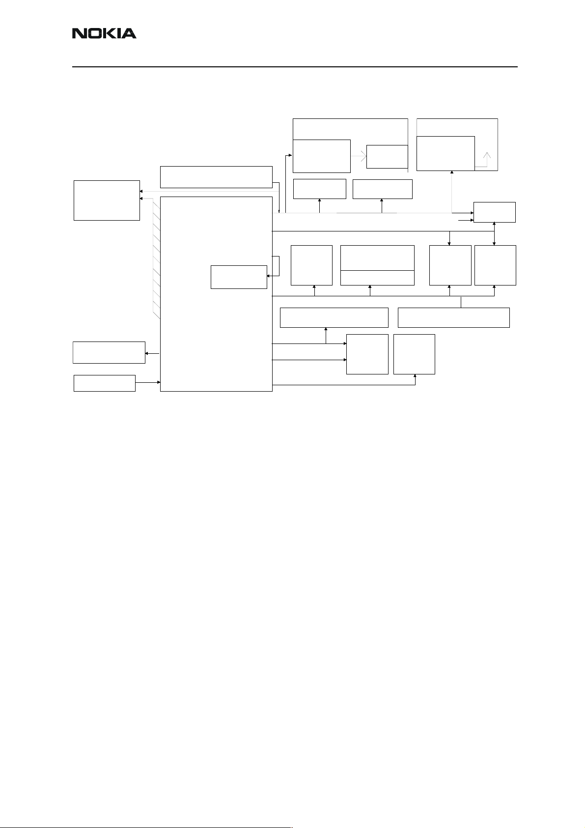
Figure 2: Baseband Block Diagram
Hallmagnet
Internal
antenna
CAMERA
LCD2
Illumination
SIM
PA
RF
Helgo
HWA
UPP
8mv3
LCD1
Illumination
On Keyboard PWB
Keyboard
Illumination
Flash 128Mbit
+
SRAM 8Mbit
FMRadio
Mo/St Amp
Hallswitch
Vibra
Vibra
UEMKEdge
Tomahawk
Page 6 Nokia Corporation. Issue 1 02/2004
IR 1.8V
Battery BL-4C
Charger
Page 7
Company confidential RH-23
CCS Technical Documentation System Module and User Interface
Environmental Specifications
Temperature Conditions
Full functionality through ambient temperature range -10 oC to +55 oC.
Reduced functionality between -25 oC to -10 oC and +55 oC to +75 oC.
Humidity and Water Resistance
Full functionality in humidity range is 5% - 95%.
Condensed or dripping water may cause intermittent malfunctions.
Protection against dripping water is implemented.
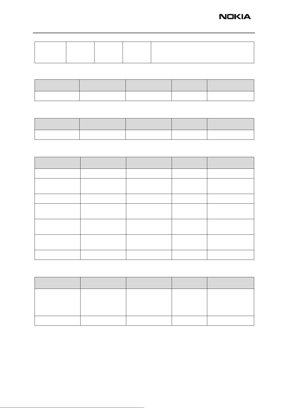
Baseband Technical Specifications
Table 1: Absolute Maximum Ratings
Signal Note
Battery Voltage (Idle) -0.3V - 5.5V
Battery Voltage (Call) Max 4.8V
Charger Input Voltage -0.3V - 16V
DC Characteristics
Regulators and Supply Voltage Ranges
Table 2: Battery Voltage Range
Signal Min Nom Max Note
VBAT 3.05V 3.6V 4.2V (charging high limit voltage) 3.05V is SW cut off
Table 3: Baseband Regulators
Signal Min Nom Max Note
VANA 2.70V 2.78V 2.86V Imax = 80mA
VFLASH1 2.70V
2.61V
VFLASH2 2.70V 2.78V 2.86V Imax = 40mA
VSIM 1.745V
2.91V
VIO 1.72V 1.8V 1.88V Imax = 150mA
2.78V 2.86V
2.96V
1.8V
3.0V
1.855V
3.09V
Imax = 70mA
Isleep= 1.5mA
Imax = 25mA
Isleep = 0.5mA
Isleep = 0.5mA
Issue 1 02/2004 Nokia Corporation. Page 7
Page 8
RH-23 Company confidential
System Module and User Interface CCS Technical Documentation
VCORE 1.492V 1.57V 1.650V Imax = 200mA
Isleep = 0.2mA default value
1.5V
Table 4: Accessory Regulator
Signal Min Nom Max Note
Vout 2.72V 2.78 2.86V Imax = 150mA
Table 5: Camera & LCD Regulator
Signal Min Nom Max Note
Vdig 1.72V 1.80V 1.88V Imax = 150mA
Table 6: RF Regulators
Signal Min Nom Max Note
VR1A / VR1B 4.6V 4.75V 4.9V Imax = 10mA
VR2 2.70V
3.20V
VR3 2.70V 2.78V 2.86V Imax = 20mA
VR4 2.70V 2.78V 2.86V Imax = 50mA
VR5 2.70V 2.78V 2.86V Imax = 50mA
VR6 2.70V 2.78V 2.86V Imax = 50mA
VR7 2.70V 2.78V 2.86V Imax = 45mA
Signal Min Nom Max Note
IPA1 and IPA2 0mA - 5mA Programmable, +/-
2.78V
3.3V
Table 7: Current Sources
2.86V
3.40V
Imax = 100mA
Isleep = 0.1mA
Isleep = 0.1mA
Isleep = 0.1mA
6%
VIPA1& VIPA2=0V-
2.7V
IPA3 and IPA4 95µA 100µA 105µA VIPA34 = 0V - 2.7V
Page 8 Nokia Corporation. Issue 1 02/2004
Page 9
Company confidential RH-23
CCS Technical Documentation System Module and User Interface
Power Distribution Diagram
Figure 3: Power Distribution Diagram
RF
RTC Battery
Charger
IPA1
IPA2
ISET
VR1A
VR1B
VR2
VR3
VR4
VR5
VR6
VR7
VBACK
VCHARIN
BATTERY
UEM
UEM
analog parts
VBAT
VBAT
VFLASH1
VANA
VFLASH2
VIO
VCORE
VSIM
ILLUMINATION
LED
drivers
VIBRA
FM-
RADIO
COMBO 128 Mbit+8Mbit
LEDs
IHF PA
CAMERA
ACCELLERATOR
UPP
Pop-Port
Accessory
Regulator
VIO
LCD1
EXTERNAL 1.8V REGULATOR
VOUT
IR
LCD2
VDIG
SIM
Issue 1 02/2004 Nokia Corporation. Page 9
Page 10
RH-23 Company confidential
System Module and User Interface CCS Technical Documentation
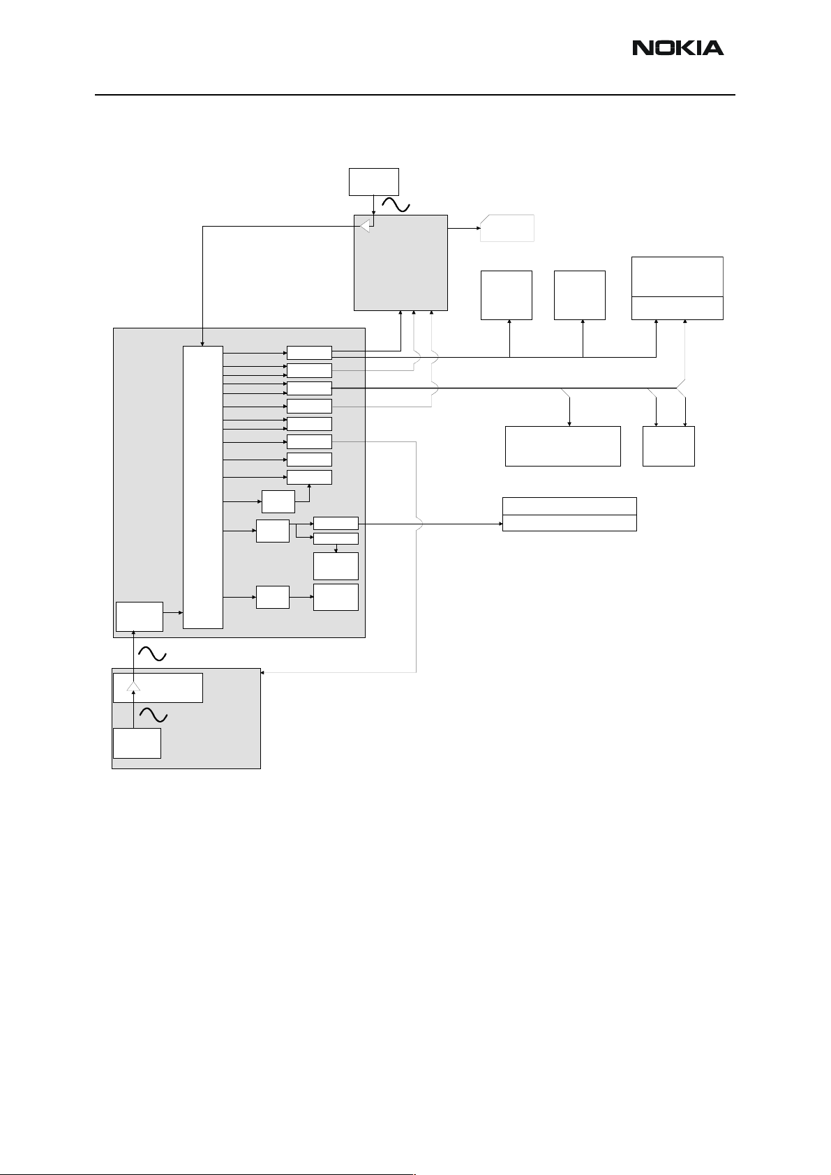
Clocking Strategy
Figure 4: Clock Distribution Diagram
32kHz XO
UPP
Clock
Slicer
CTSI
UIFClk
SIMClk
MCCLK
MBusUS ARTClk
GenI OUSARTClk
RxMClk
MFIC lk
PDCClk
SCUClk
CoderClk
AccClk
AccPLLClk
MCUCl k
MCUClk
PLL
PLL
PLL
UIF
SIMIF
PUP
RxModem
MFI
SCU
Coder
ACCIF
EXTBUSC
ARM7
SleepClk
MEMIF
Lead3
UEM
CBUSClk
SIMCardClk
DBUSClk
FLSClk
SIMClkO
LCDCamClk
SIM
LCD1
LCD2
CLK
MONO/STEREO
AMPLIFIER
MEMORIES
COMBO 128Mbit+8Mbit
CAMERA
ACCELLERATOR
GENIO3/
CLK
GENIO 11/
FMCtrlCl k
GENIO 15/
GENIO 24/
FMClk
FM-
RADIO
RFClk
OSC_IN
26MHz
VCTCXO
RFBusClk
HELGO
RF
Page 10 Nokia Corporation. Issue 1 02/2004
Page 11
Company confidential RH-23
CCS Technical Documentation System Module and User Interface
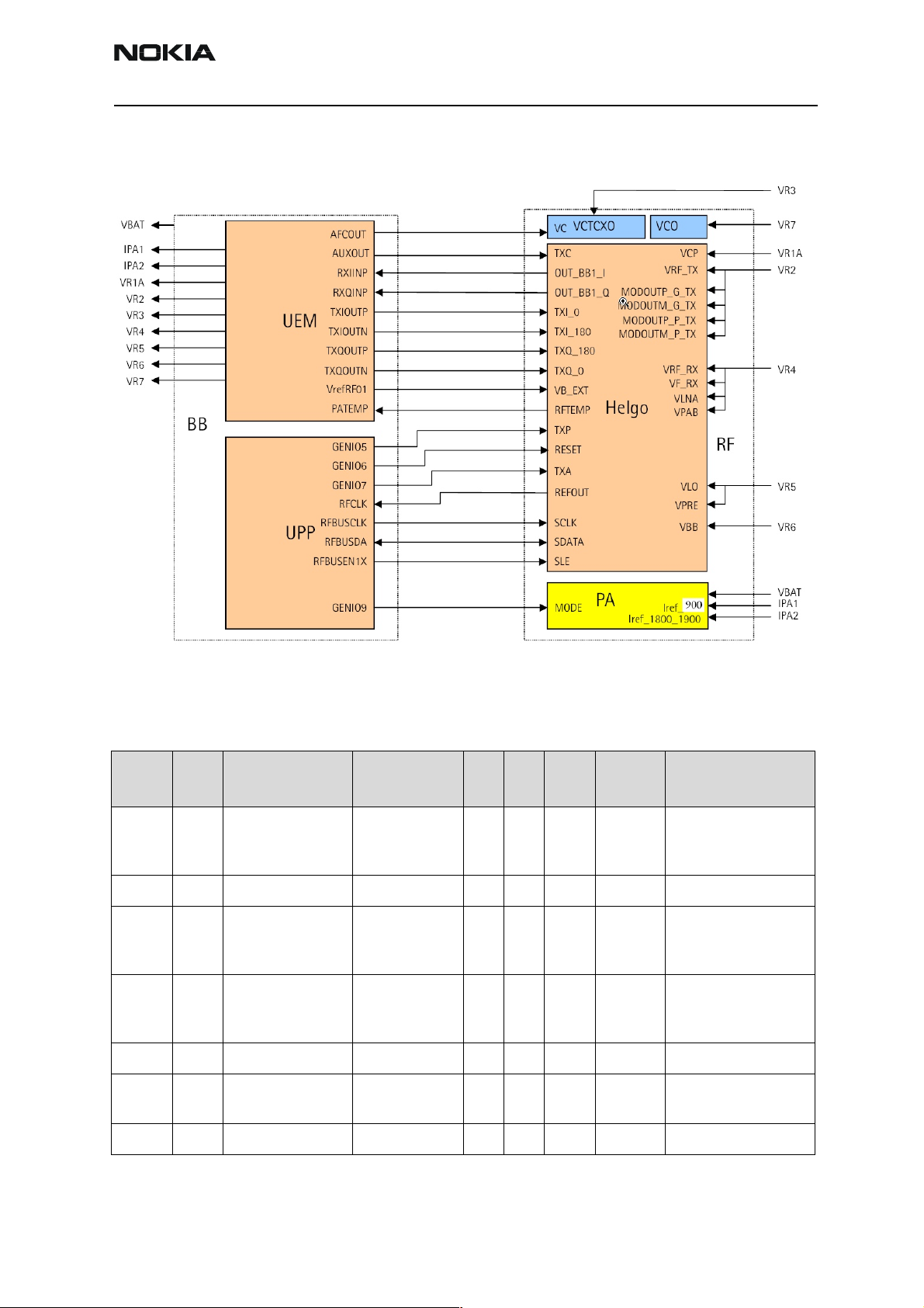
RF/BB Interface
Figure 5: RF/BB Connections
Table 8: AC and DC Characteristics of RF-Baseband Voltage Supplies
Signal
VBAT Bat-
VR1A
VR1B
VR2 UEM HELGO Voltage 2.702.782.86 V Supply for I/Q-modu-
Fro
m
tery
UEM HELGO Voltage 4.6 4.754.9 V Supply for charge
To Parameter
PA, UEM, LED
drivers, IHF PA,
Vibra and IR
Voltage 2.953.6 4.2 V Battery supply. Cut-
Current 2000 mA
Current drawn
by PA when
”off”
Current 2 10 mA
Current 65 100 mA
Mi
Typ Max Unit Function
n
0.8 2 µA
off level of DCT4 regulators is 3.05V.
pump for SHF VCO
tuning.
lators, buffers, ALS
Issue 1 02/2004 Nokia Corporation. Page 11
Page 12
RH-23 Company confidential
System Module and User Interface CCS Technical Documentation
VR3 UEM VCTCXO, HELGO Voltage 2.702.782.86 V Supply for VCTCXO,
PLL digital parts
Current 1 20 mA
VR4 UEM HELGO Voltage 2.702.782.86 V Supply for Helgo RX;
PA bias blocks.
Current 50 mA
VR5 UEM HELGO Voltage 2.702.782.86 V Supply for Helgo PLL;
dividers, LO-buffers,
prescaler
Current 50 mA
VR6 UEM HELGO Voltage 2.702.782.86 V Supply for Helgo BB
and LNAs
Current 50 mA
VR7 UEM SHF VCO Voltage 2.702.782.86 V Supply for SHF VCO
Current 30 mA
VrefRF01UEM HELGO Voltage 1.3341.351.366V Voltage Reference for
HELGO DCN2
op.amps.
Current 100 µA
VrefRF02UEM VB_EXT Voltage 1.3341.351.366V Voltage reference for
HELGO bias block.
Current 100 µA
Page 12 Nokia Corporation. Issue 1 02/2004
Page 13
Company confidential RH-23
CCS Technical Documentation System Module and User Interface
Table 9: AC and DC Characteristics of RF-Baseband Digital Signals
Input characteistics
Signal Front To Parameter
Min Typ Max Unit
TXP UPP (GenIO5) HELGO ”1” 1.38 1.88 V Power amplifier
”0” 0 0.4 V
TXA UPP (GenIO7) HELGO ”1” 1.38 1.88 V Power control
”0” 0 0.4 V
MODE UPP (GenIO9) PA ”1” 1.38 1.88 V GSM/EDGE mode
”0” 0 0.4 V
RFBusEna1XUPP HELGO ”1” 1.38 1.88 V RFbus enable
Function
enable
loop enable
selection
”0” 0 0.4 V
RFBusData
RFBusClk UPP HELGO ”1” 1.38 1.88 V RFBus clock
RESET UPP (GENIO6) HELGO ”1” 1.38 1.85 V Reset to HELGO
Signal name From To Parameter
VCTCXO VCTCXO
UPP HELGO ”1” 1.38 1.88 V RFbus data; read/
write
”0” 0 0.4 V
”0” 0 0.4 V
Data frequency 10 MHz
”0” 0 0.4 V
Table 10: AC and DC Characteristics of DCT4 RF-Baseband Analogue Signals
Mi
n
UPP Frequency 26 MHzHigh stability
(buffered
in HELGO)
Typ
MaxUni
t
Function
clock signal for
the logic circuits,
AC coupled.
Signal amplitude 0.2 0.8 2.0 Vp
p
Duty Cycle 40 60 %
VCTCXOGnd VCTCXO UPP DC Level 0 V Ground for
VCTCXO
RXI/RXQ HELGO UEM Voltage swing
(static)
1.351.4 1.45VppReceived demodulated IQ signals
Issue 1 02/2004 Nokia Corporation. Page 13
Page 14
RH-23 Company confidential
System Module and User Interface CCS Technical Documentation
DC level 1.3 1.351.4 V
TXIP / TXIN UEM HELGO Differential voltage
swing (static)
DC level 1.171.201.23V
TXQP / TXQN UEM HELGO Same specification as for TXIP / TXIN Q-signal
AFC UEM VCTCXO Voltage Min
Max
TxC UEM HELGO Voltage Min
Max
RFTemp HELGO UEM Voltage at -20oC 1,5
Voltage at +25oC 1,7
Voltage at +60oC 1,7
DC_sense PA UEM Voltage 0.6 V PA final stage
2.152.2 2.25VppI-signal
0.0
2.4
2.4
0.1
V Automatic fre-
2.6
0.1 V Transmitter power
7
9
quency control for
VCTCXO
level and ramping
control
V Temperature sen-
sor of RF
quiescent current
level information
IPA1 / IPA2 UEM PA Output Voltage 0 2.7 V PA final stage
quiescent current
adjustment
Current range 0 5 mA
Current tolerance -6 +6 %
Baseband functional description
Modes of operation
RH-23 baseband engine has six different functional modes:
1 No supply
2 Backup
3Acting Dead
4Active
Page 14 Nokia Corporation. Issue 1 02/2004
Page 15

Company confidential RH-23
CCS Technical Documentation System Module and User Interface
5 Sleep
6 Charging
No Supply
In NO_SUPPLY mode, the phone has no supply voltage. This mode is due to disconnection
of main battery and backup battery or low battery voltage level in both of the batteries.
Phone is exiting from NO_SUPPLY mode when sufficient battery voltage level is detected.
Battery voltage can rise either by connecting a new battery with VBAT > VMSTR+ or by
connecting charger and charging the battery above VMSTR+.
Back_Up
In BACK_UP mode the backup battery has sufficient charge but the main battery can be
disconnected or empty (VBAT < VMSTR+ and VBACK > VBUCOFF). VRTC regulator is disabled
in BACK_UP mode. VRTC output is supplied without regulation from backup battery
(VBACK). All the other regulators are disabled in BACK_UP mode.
Acting Dead
If the phone is off when the charger is connected, the phone is powered on but enters a
state called ”Acting Dead”. To the user, the phone acts as if it was switched off. A battery-charging alert is given and/or a battery charging indication on the display is shown
to acknowledge the user that the battery is being charged.
Active
In the Active mode the phone is in normal operation, scanning for channels, listening to
a base station, transmitting and processing information. There are several sub-states in
the active mode depending on if the phone is in burst reception, burst transmission, if
DSP is working etc.
One of the sub-states of the active mode is FM radio on state. In that case, Audio Amplifier and FM radio are powered on. FM radio circuitry is controlled by the MCU and
32kHz-reference clock is generated in the UPP. VFLASH2 regulator is operating.
In Active mode the RF regulators are controlled by SW writing into UEM’s registers
wanted settings: VR1A can be enabled or disabled. VR2 can be enabled or disabled and
its output voltage can be programmed to be 2.78V or 3.3V. VR4 -VR7 can be enabled,
disabled, or forced into low quiescent current mode. VR3 is always enabled in Active
mode.
Sleep Mode
Sleep mode is entered when both MCU and DSP are in stand–by mode. Both processors
control sleep-mode. When SLEEPX signal ‘low’ is detected UEM enters SLEEP mode.
VCORE, VIO and VFLASH1 regulators are put into low quiescent current mode. All the RF
regulators are disabled in SLEEP. When SLEEPX signal ‘high’ is detected UEM enters
ACTIVE mode and all functions are activated.
Issue 1 02/2004 Nokia Corporation. Page 15
Page 16

RH-23 Company confidential
System Module and User Interface CCS Technical Documentation
The sleep mode is exited either by the expiration of a sleep clock counter in the UEM or
by some external interrupt, generated by a charger connection, key press, headset connection etc.
In sleep mode VCTCXO is shut down and 32 kHz sleep clock oscillator is used as reference
clock for the baseband.
Charging
Charging can be performed in parallel with any operating mode. The battery type/size is
indicated by a BSI-resistor inside the battery pack. The resistor value corresponds to a
specific battery capacity. This capacity value is related to the battery technology as different capacity values are achieved by using different battery technology.
The battery voltage, temperature, size and current are measured by the UEM controlled
by the charging software running in the UPP.
The charging control circuitry (CHACON) inside the UEM controls the charging current
delivered from the charger to the battery. The battery voltage rise is limited by turning
the UEM switch off when the battery voltage has reached 4.2 V. Charging current is
monitored by measuring the voltage drop across a 220 mΩ resistor.
Power Up and Reset
UEM ASIC controls reset and power up. RH-23 baseband can be powered up in following
ways:
1 Press power button which means grounding the PWRONX pin on UEM
2 Connect the charger to the charger input
3 Supply battery voltage to the battery pin.
4 RTC alarm power up
After receiving one of the above signals, the UEM counts a 20ms delay and then enters
its reset mode. The watchdog starts up, and if the battery voltage is greater than Vcoff+
a 200ms delay is started to allow references etc. to settle. After this delay elapses the
VFLASH1 regulator is enabled. 500us later VR3, VANA, VIO and VCORE are enabled.
Finally the PURX line is held low for 20 ms. This reset, PURX, is fed to the baseband ASIC
UPP, resets are generated for the DSP and the MCU. During this reset phase the UEM
forces the VCXO regulator on regardless of the status of the sleep control input signal to
the UEM. All baseband regulators are switched on at the UEM power on except for the
SIM regulator that is controlled by the MCU. The UEM internal watchdog is running during the UEM reset state, with the longest watchdog time selected. If the watchdog
expires, the UEM returns to power off state.
Page 16 Nokia Corporation. Issue 1 02/2004
Page 17

Company confidential RH-23
CCS Technical Documentation System Module and User Interface
Power Up with PWR key
When the Power on key is pressed the UEM enters the power up sequence as described in
the previous paragraph. Pressing the power key causes the PWRONX pin on the UEM to
be grounded. The UEM PWRONX signal is not part of the keypad matrix. The power key is
only connected to the UEM. This means that when pressing the power key an interrupt is
generated to the UPP that starts the MCU. The MCU then reads the UEM interrupt register and notice that it is a PWRONX interrupt. The MCU now reads the status of the
PWRONX signal using the UEM control bus, CBUS. If the PWRONX signal stays low for a
certain time the MCU accepts this as a valid power on state and continues with the SW
initialization of the baseband. If the power on key does not indicate a valid power on situation, the MCU powers off the baseband.
Power Up when Charger is connected
In order to be able to detect and start charging in a case where the main battery is fully
discharged (empty) and hence UEM has no supply (NO_SUPPLY or BACKUP mode of
UEM) charging is controlled by START-UP CHARGING circuitry.
Whenever VBAT level is detected to be below master reset threshold (VMSTR-) charging
is controlled by START_UP charge circuitry. Connecting a charger forces VCHAR input to
rise above charger detection threshold, VCHDET+. By detection start-up charging is
started. UEM generates 100mA constant output current from the connected charger’s
output voltage. As battery charges its voltage rises, and when VBAT voltage level higher
than master reset threshold limit (VMSTR+) is detected START_UP charge is terminated.
Monitoring the VBAT voltage level is done by charge control block (CHACON). MSTRX=‘1’
output reset signal (internal to UEM) is given to UEM’s RESET block when VBAT>VMSTR+
and UEM enters into reset sequence as described in section Power Up and Reset.
If VBAT is detected to fall below VMSTR- during start-up charging, charging is cancelled.
It will restart if new rising edge on VCHAR input is detected (VCHAR rising above VCHDET+).
Power Up when Battery is connected
Baseband can be powered up by connecting battery with sufficient voltage. Battery voltage has to be over UEM internal comparator threshold level, Vcoff+. When battery voltage is detected, UEM enters to reset sequence as described in section Power Up and
Reset.
Phone can be powered up to LOCAL mode by setting BSI resistor 3.3kΩ. This causes MCU
to wake up directly when battery voltage is supplied.
RTC Alarm Power Up
If phone is in power off mode when RTC alarm occurs the wake up procedure is as
described in section Power Up and Reset. After baseband is powered on, an interrupt is
given to MCU. When RTC alarm occurs during power on state the interrupt for MCU is
generated.
Issue 1 02/2004 Nokia Corporation. Page 17
Page 18

RH-23 Company confidential
System Module and User Interface CCS Technical Documentation
A/D Channels
The UEM contains the following A/D converter channels that are used for several measurement purposes. The general slow A/D converter is a 10-bit converter using the UEM
interface clock for the conversion. An interrupt will be given at the end of the measurement.
The UEM’s 11-channel analog to digital converter is used to monitor charging functions,
battery functions, user interface and RF functions.
A/D-channels used by RH-23:
BTEMP, Battery Temperature estimation, NTC pull down resistor in BTEMP line
BSI, Battery Size Indicator
VBAT, Battery voltage
VCHAR, Charging voltage
ICHAR, Charging current
HOOKINT, Eg. Headset-button detection
HEADINT, Accessory detection connected to ACI line in Pop-Port
PATEMP, RFIC temperature, connected to Helgo
VCXOTEMP, RF PA type detection, R715
KEYB1, Fold detection, connected to Hall switch
Fold detection switch
Fold position detection is implemented with Hall switch TLE4917 that is located in lower
block and magnet locating in upper block Hall switch output is connected to KEYB1 ADchannel.
• When Fold is closed (magnet near switch) output is pulled high to
VFLASH1
• When fold is open output is low, 0V
PRG pin is connected to GND. PRG determines the output state when magnet is not near.
Page 18 Nokia Corporation. Issue 1 02/2004
Page 19

Company confidential RH-23
CCS Technical Documentation System Module and User Interface
Figure 6: Hall Switch connection to UEM
Battery
A 760mAh Li-ion battery pack BL-4C is used in RH-23. Other battery packs are not plan
to be used.
Table 11: BL-4C Characteristics
Description Value
Nominal discharge cut-off voltage 3.1V
Nominal battery voltage 3.6V
Nominal charging voltage 4.2V
Maximum charger output current 850 mA
Minimum charger output current 200 mA
Table 12: Pin Numbering of Battery Pack
Signal name Function
VBAT Positive battery terminal
BSI Battery capacity measurement (fixed resistor inside the battery pack)
GND Ground/negative/common battery terminal
Issue 1 02/2004 Nokia Corporation. Page 19
Page 20

RH-23 Company confidential
System Module and User Interface CCS Technical Documentation
Figure 7: Battery pack contacts
Charging
Supported chargers are AC-1, ACT-1, ACP-7, ACP-8, ACP-9, ACP-12, LCH-8, LCH-9 and
LCH-12.
Charging is controlled by the UEM and external components are needed for EMC, reverse
polarity and transient protection of the input to the baseband module. The charger connection is through the system connector interface.
The operation of the charging circuit has been specified in such a way as to limit the
power dissipation across the charge switch and to ensure safe operation in all modes.
Table 13: Charging Connector characteristics
Pin Signal Min Nom Max Condition Note
1 VCHAR 11 . 1 V pe ak 16.9 Vpeak
7.9 Vrms
1.0 Apeak
7.0 Vrms 8.4 Vrms 9.2 Vrms
850 mA
2 GND 0 Charger ground
Standard charger Charger positive input
Fast charger
Stereo FM Radio
RH-23 is using the same FM radio module as HDb12 and HDb18. FM radio circuitry is
implemented by using highly integrated radio IC, TEA5767. TEA5767 is a single-chip
electronically tuned FM stereo radio with fully integrated IF selectivity and demodulation. The IF-frequency is 225 kHz. The radio is completely adjustment-free and does only
require a minimum of small and low cost external components. It has signal dependent
mono/stereo blend [Stereo Noise Cancelling (SNC)]. The radio can tune the European, US
and Japan FM bands. Channel tuning and other controls are controlled through serial bus
interface by the MCUSW. Reference clock, 32kHz, is generated by the UPP CTSI block
(routed from sleep clock).
Page 20 Nokia Corporation. Issue 1 02/2004
Page 21

Company confidential RH-23
CCS Technical Documentation System Module and User Interface
Figure 8: Digital interface connection
Table 14:
BB Signal
VFLASH2 Vcca 2.7V 2.78V2.86V Imax =10.5 mA
GenIO(24) FMClk 1.4V01.8V 1.88V
GenIO(8) FMWrEn 1.4V0V1.8V 1.88V
GenIO(12) FMCtrlDa 1.4V01.8V 1.88V
FM Radio
Signal
Vcc(vco) 2.7V 2.78V2.86V Imax =940 µA
Vccd 2.7V 2.78V2.86V Imax = 3.9 mA
Min Nom Max Condition Note
32kH
z
30pp
m
FM Radio Interface
High
0.4V
0.4V
0.6V
Low
Frequency
Stability
High
Low
High
Low
Reference clock for FM
radio module
Write/Read enable
Bi-directional data
GenIO(11) FMCtrlClk 1.4V01.8V 1.88V
0.6V
1MHz Frequency
FM
Antenna
RFI1, RFI2 76M
Hz
108
MHz
High
Low
FM Input frequency
Issue 1 02/2004 Nokia Corporation. Page 21
Page 22

RH-23 Company confidential
System Module and User Interface CCS Technical Documentation
FM Radio L
FM Radio R
VAFL
VAFR
Camera
Technical Summary
Camera is a VGA-type with built-in auto functions such as white-balance control, multiple read, automatic color correction etc. HW accelerator will be used for white balancing
and other needed picture processing functions. Camera module is located on upper block
part of phone and is connected to camera accelerator via flex connection. Accelerator is
connected to UPP via same UIF bus, which displays are using.
The interface to camera is bi-directional: 8-bit control data can be transmitted from UPP
to camera and 8/16-bit data can be transmitted from camera to UPP.
100
mV
24dB 30dB Channel separation
54dB 60dB (S+N)/N
2% Harmonic distortion
Figure 9: Camera and HWA connections to the baseband
Audio level
Page 22 Nokia Corporation. Issue 1 02/2004
Page 23

Company confidential RH-23
CCS Technical Documentation System Module and User Interface
Table 15: HWA Power Supply characteristics
Signal name Type Min Typ Max Unit Description
Vdd PWR 1.7 1.8 1.9 V Digital Power Supply
Vpp PWR 2.7 2.78 2.9 V Embedded DRAM VPP
Table 16: HWA signals Table 17a: HWA DC characteristics for Digital IOs
Signal Type Description Symbol Parameter Min Max Unit
MSCL I/O Master CCI serial
clock
MSDA I/O Master CCI serial data Vih High level input
RQN I, subLVDS CPP receiver CK- Vol Low level output
RQN I, subLVDS CPP receiver CK+ Voh High level output
RDN I, sub-
LVDS
RDP I, sub-
LVDS
DACLK I UIF Serial data clock
RXDA I UIF Data to receive
TXDA O UIF data to transmit
CSX I UIF Chip Select
CE I Chip Enable(active
CPP receiver D-
CPP receiver D+
high)
Vil Low level input
voltage
voltage
voltage
voltage
0.3*Vdd V
0.7*Vdd V
0.2*Vdd V
0.8*Vdd V
CLK I System Clock
Table 17: Camera Power Supply characteristics
Signal name Type Min Typ Max Unit Description
VDIG PWR 1.7 1.8 1.9 V Digital Power Supply
VANA PWR 2.7 2. 8 2.9 V Analogue Supply
Issue 1 02/2004 Nokia Corporation. Page 23
Page 24

RH-23 Company confidential
System Module and User Interface CCS Technical Documentation
Table 18: Camera Signals Table 18a: Camera DC Characteristics for Digital IOs
Signal Type Description Symbol Parameter Min Max Un.
XSHUTDOWN
CCISCL I/O CCI bus serial
CCISDA I/O CCI bus serial
CCPCLKN O, sub-
CCPCLKP O, sub-
CCPDATAN O, sub-
CCPDATAP O, sub-
Signal name Type Min Typ Max Unit Description
I Power down con-
trol
clock
data
CCP Clock+ ve
LVDS
LVDS
LVDS
LVDS
phase
CCP Clock -ve
phase
CCP Data +ve
phase
CCP Data -ve
phase
Table 19: Camera EXTCLK parameters
Vil Low level input volt-
age
Vih High level input volt-
age
Vol Low level output
voltage
Voh High level output
voltage
0.7*
VDIG
0.8*
VDIG
0.3*VDIGV
V
0.2*VDIGV
V
EXTCLK I VDIG V External system clock, DC-coupled
13.00 MHz
Page 24 Nokia Corporation. Issue 1 02/2004
Page 25

Company confidential RH-23
CCS Technical Documentation System Module and User Interface
Compact Camera Port (CCP)
Figure 10: CCP interface
Camera Module HWA
Parallel
to
Serial
Converter
CCPCLKP
CCPCLKN
CCPDATAP
CCPDATAN
Serial
to
Parallel
Converter
SubLVDS Receivers SubLVDS Transmitters
The Compact Camera Port (CCP) consists of bit-serial data and a data qualification clock.
The bit-serial data and data qualification clock are transmitted differentially via SubLVDS transmitter pads
The CCP interface utilizes SubLVDS I/O that provides 1.8 V-operated differential signalling over short distances. Modified LVDS type current mode transmitters / receivers are
used, and optimized for maximum driving symmetry. SubLVDS enables the use of high
data rates with low EMI.
Table 20: CCP (subLVDS) Transmitter Signal Specifications
Parameter Min Typ Max Unit
Common mode voltage 1.7 1.8 1.9 V
Differential voltage swing (based on 100Ω +/-5% terminating resistor) 100 150 200 mV
Drive current range(internally set by bias circuit) 0.5 1.5 2 mA
Output impedance 40 140 W
Rise time and Fall time 300 500 ps
Issue 1 02/2004 Nokia Corporation. Page 25
Page 26

RH-23 Company confidential
System Module and User Interface CCS Technical Documentation
LCD displays
RH-23 has two separate LCD displays:
• Primary LCD used is 128 x 128 matrix, 12 bpp (bits per pixel), active matrix color display.
• Secondary LCD is 96x36 dot matrix FSTN Black & White display.
Both displays are connected to BB by UPP UIF- serial bus. Maximum transfer speed is
6.5Mhz for primary display and 3.25MHz for secondary display. VGA-camera is also using
same UIF- bus as LCD displays . Separate CSX pins do switching between devices.
Figure 11: UIF interface
CAM
CCPDATAN/P
XSHUTDOWN
LCD1
CCISCL
CCISDA
CCPCLKN/P
EXTCLK
SDA
SCLK
RESX
CSX
MSCL
MSDATA
RQN/P
RDN/P
DACLK
RXDA
TXDA
CSX
CE
CLK
CamCtrClk
CamVCtr
HWACSX
CAMRxDa
LCDCamTxDa
LCDCamClk
LCDResX
LCDCSX
CSX2
HWA
UPP
LCD2
Page 26 Nokia Corporation. Issue 1 02/2004
RESX
SCLK
SDA
CSX
Page 27

Company confidential RH-23
CCS Technical Documentation System Module and User Interface
Table 21: LCD1 and LCD2 Power Supply characteristics
Signal Min Typ Max Unit Description
VDD 2.70 2.78 2.86 V Supply voltage. connected to VFLASH1
VDDI 1.72 1.8 1.88 V Logic supply voltage, connected to VDIG
Table 22: LCD1 and LCD2 DC characteristics for Digital IOs
Symbol Parameter Min Max Unit
Vil Low level input voltage 0.3*VDDI V
Vih High level input voltage 0.7*VDDI V
Vol Low level output voltage 0.22*VDDI V
Voh High level output voltage 0.8*VDDI V
Table 23: DC Characteristics for VLED+ lines
Symbol Parameter Typ Max Unit
VLED+ Forward voltage Vf over LED when LED ON 3.6 4 V
Forward voltage Vf over LED when LED OFF 0 V
Table 24: LCD1 (Color display) Connector Table 24a:LCD2 (Color display) Connector
Pin Signal Type Note Pin Signal Type Note
1 VDD PWR Voltage supply 1 VDD PWR Voltage supply
2 VDDI PWR Logic supply 2 VDDI PWR Logic supply
3 SDA I/O Serial data Input/Output 3 SDA I/O Serial data Input/
Output
4 GND PWR Ground 4 GND PWR Ground
5 NC Not connected 5 SCLK I Serial clock,
3.25MHz
6 GND PWR Ground 6 GND PWR Ground
7 SCLK I Serial clock, 6.5MHz 7 RESX I Reset, Active low
8 GND PWR Ground 8 GND PWR Ground
9 RESX I Reset, Active low 9 CSX I Chip select, Active
low
10 CSX I Chip select, Active low 10 GND PWR Ground
11 GND PWR Ground 11 GND PWR Ground
12 EAR Connected to GND 12 VLED+ PWR LED Supply voltage
Issue 1 02/2004 Nokia Corporation. Page 27
Page 28

RH-23 Company confidential
System Module and User Interface CCS Technical Documentation
13 GND PWR Ground 13 LEDGND PWR LED return current
14 EAR Connected to GND 14 GND PWR Ground
15 VDD PWR Voltage supply 15 VDD PWR Voltage supply
16 VLED+ PWR LED Supply voltage 16 GND PWR Ground
17 LEDGND PWR LED return current 17 GND PWR Ground
18 VLED+ PWR LED Supply voltage 18 GND PWR Ground
19 VLED+ PWR LED Supply voltage 19 GND PWR Ground
20 GND PWR Ground 20 GND PWR Ground
Keyboard and LCD Illumination
In RH-23, white LEDs are used for LCD and keypad illumination. Three LEDs are used for
primary LCD, one LED for secondary LCD and four LEDs for keyboard illumination. LCD
backlight-LEDs are located inside LCD modules.
Figure 12: Keyboard LED driver
Keyboard LEDs use 4-channel, charge-pump type, white LED driver (LM2795) that is
enabled by the UEM KLIGHT by setting PWM to 100% (~0V). Resistor connected to ISET
pin of the driver determines LED current.
Both LCDs share one similar driver the keyboard illumination is using, LM2795. Driver is
enabled by GENIO(20). LCD1 LED cathodes are all connected to KLIGHT and LCD2 LED
cathode is connected to DLIGHT. Because only one LCD is illuminated at time it is possible to activate either LCD1 or LCD2 illumination by sinking the LED current through
KLIGHT or DLIGHT.
• When LCD1 is illuminated current flows through LCD1 LEDs to KLIGHT and ground.
• When LCD2 is illuminated current flows through LCD2 LED to DLIGHT and ground.
Because LCD1 LED requires more current than LCD2 GENIO(21) is connected to BRGT
through resistive divider to increase LED current. BRGT is analog brightness control pin of
LM2795.
Page 28 Nokia Corporation. Issue 1 02/2004
Page 29

Company confidential RH-23
CCS Technical Documentation System Module and User Interface
• When LCD2 is illuminated GENIO(21) is set to ‘0’. ISET resistor determines the current.
• When LCD1 is illuminated GENIO(21) is set to ‘1’ (1.8V) and LED current is boosted.
Figure 13: LCD1 and LCD2 LED driver diagram
VBAT
LM2795
SD
GENIO(20)
GENIO(21)
68k
BRGT
33k
ISET
270R
LCD2
LCD1
IR Module
The IR link supports speed from 9600 bit/s to 1.152 MBit/s up to distance of 80 cm.
Transmission over the IR is half-duplex. The length of the transmitted IR pulse depends
on the speed of the transmission. IR transceiver can be set into shutdown mode by setting SD pin to logic ’1’ for current saving reasons. VBAT supplies transmitter LED, VIO
supplies I/O parts and VFLASH1 other parts of the transceiver. RX and TX data lines are
connected directly to UPP, not through UEM.
KLIGHT
UEM
VBAT
KLIGHT
Figure 14: IR interface
DLIGHT
VBAT
DLIGHT
Vibra
A vibra alerting device is used to generate a vibration signal for an incoming call. Vibra
connection is done with spring contacts via additional vibra lifting part PWB. Vibra inter-
Issue 1 02/2004 Nokia Corporation. Page 29
Page 30
RH-23 Company confidential
System Module and User Interface CCS Technical Documentation
face is the same like other DCT4 projects. The vibra is controlled by a PWM signal from
the UEM
UI Board (Keyboard)
RH-23 has separate UI board, named as 1BF, which includes contacts for the keypad
domes and 4 LED’s for keypad lighting. 4 resistors beside each LED are for ESD purposes
and connected to GND from both ends. UI board is connected to main PWB through 20
pole board-to-board connector with springs.
Keyboard is Douglas 4 style and 6x5-matrix keyboard is for controlling the keyboard. Key
pressing is detected by scanning procedure. Keypad signals are connected UPP keyboard
interface.
When no key is pressed, row inputs are high due to UPP internal pull-up resistors. The
columns are written zero. When key is pressed one row is pulled down and an interrupt is
generated to MCU. After receiving interrupt, MCU starts scanning procedure. All columns
are first written high and then one column at the time is written down. All other columns except one, which was written down, are set as inputs. Rows are read while column at the time is written down. If some row is down it indicates that key which is at
the cross point of selected column and row was pressed. After detecting pressed key all
register inside the UPP are reset and columns are written back to zero.
Table 25: Keyboard (board-to-board) Connector
Pin Signal Note
1 GND Ground
2 ROW(4) Keyboard matrix row 4
3 ROW(3) Keyboard matrix row 3
4 COL(2) Keyboard matrix column 2
5 ROW(2) Keyboard matrix row 2
6 COL(1) Keyboard matrix column 1
7 ROW(0) Keyboard matrix row 0
8 ROW(1) Keyboard matrix row 1
9 COL(3) Keyboard matrix column 3
10 COL(4) Keyboard matrix column 4
11 GND Ground
12 ROW(5) Keyboard matrix row 5
13 GND Ground
14 VLED1+ Supply Voltage for Keyboard LED
15 VLED2+ Supply Voltage for Keyboard LED
16 VLED3+ Supply Voltage for Keyboard LED
Page 30 Nokia Corporation. Issue 1 02/2004
Page 31

Company confidential RH-23
CCS Technical Documentation System Module and User Interface
17 VLED4+ Supply Voltage for Keyboard LED
18 GND Ground
19 GND Ground
20 GND Ground
Table 26: DC Characteristics for ROW and COL lines
Symbol Parameter Min Max Unit
Voh Low level output voltage 0 0.3*VIO V
Vol High level output voltage 0.7*VIO VIO V
Table 27: DC Characteristics for VLED+ lines
Symbol Parameter Typ Max Unit
VLED1+ to
VLED4+
Forward voltage Vf over LED when LED ON 3.6 4 V
Forward voltage Vf over LED when LED OFF 0 V
SIM Interface
SIM card reader is located on upper block part of phone and is connected to UEM via
hinge flex. The UEM contains the SIM interface logic level shifting. The SIM interface can
be programmed to support 3V and 1.8V SIM
The SIM power up/down sequence is generated in the UEM. This means that the UEM
generates the RST signal to the SIM. In addition, the SIMCardDet signal is connected to
UEM. Detection for SIM card removal is done with switch integrated to SIM card reader.
Switch is connected to UEM SIMCardDet pin. UEM will automatically power down the
SIM card interface within 5ms if card is removed. This is done to avoid the defected SIM
cards. A comparator inside UEM does the monitoring of the SimCardDet signal. The SIM
interface is powered up when the SIMCardDet signal indicate ”Card in”.
Table 28: SIM interface signals
Pin Name Type Purpose
1 VSIM PWR Supply voltage
2 SIMRST O SIM reset
3 SIMCLK O SIM clock
5 GND PWR Ground
6 NC Not connected
7 SIMDATA I/O SIM Data
8 S2 I SIMCARDDET
Issue 1 02/2004 Nokia Corporation. Page 31
Page 32

RH-23 Company confidential
System Module and User Interface CCS Technical Documentation
9 S1 PWR GND
Table 29: VSIM characteristics
Signal name Min Typ Max Unit
VSIM 1.8V card 1.6 1.8 1.9 V
VSIM 1.8V card 2.7 2.78 2.9 V
Table 30: DC Characteristics for SIM IO’s
Symbol Parameter Min Max Unit
Vil Low level input voltage 0.15*VSIM V
Vih High level input voltage 0.7*VSIM V
Vol Low level output voltage 0.15*Vdd V
Voh High level output voltage 0.9*Vdd V
Table 31: DC characteristics for SIMCardDet
Parameter Min Typ Max Unit
SIMCardDet voltage, SIM present 0 V
SIMCardDet voltage, switch open 2.7 2.78 2.86 V
SIMCardDet, BSI comparator Threshold 1.94 2.1 2.26 V
SIMCardDet, BSI comparator Hysteresis 50 75 100 mV
Page 32 Nokia Corporation. Issue 1 02/2004
Page 33

Company confidential RH-23
CCS Technical Documentation System Module and User Interface
Pop-Port connector
Table 32: Pop-Port connector features
Function Note
Charging Pads for 2 -wire charging in cradles
Audio - 4 -wire fully differential stereo audio output
- 2-wire differential microphone input
- FM radio antenna connection
Power Supply for Accessories 2.78V/70 mA output to accessories
ACI (Accessory Control Interface) Accessory detection/removal & controlling
FBUS Standard FBUS
USB (Optional) Not used in RH-23
Figure 15: Pop-Port Connecto
Table 33: Pop-Port Connector Signals
Pin Signal Description Signal levels Notes
1 CHARGE V Charge 0-9 V / 0.85 A
2 GND Charge GND 0.85 A
3 ACI ACI Dig 0 / 2.78V Insertion & removal detection
4 VOUT DC out 2.78V / 70mA
5 NC Not connected
6 FBUS RX 0 / 2.78V
7 FBUS TX 0 / 2.78V
8 GND Data GND
9 XMIC N Audio in 1Vpp & 2.78V Ext. Mic Input
Issue 1 02/2004 Nokia Corporation. Page 33
Page 34

RH-23 Company confidential
System Module and User Interface CCS Technical Documentation
10 XMIC P Audio in 1Vpp & 2.78V Ext. Mic Input
11 HSEAR N Audio out 1Vpp Ext. audio out (left)
12 HSEAR P Audio out 1Vpp Ext. audio out (left)
13 HSEAR R N Audio out 1Vpp Ext. audio out (right)
14 HSEAR R P Audio out 1Vpp Ext. audio out (right)
ACI, Accessory Control Interface
ACI is point-to-point, bi-directional serial bus. It has three main features:
1 The insertion and removal detection of an accessory device
2 Acting as a data bus, intended mainly for control purposes
3 The identification and authentication of accessory type which is connected
The accessories are detected by the HeadInt-signal when the plug is inserted. Normally
when accessory is not present, the pull-up resistor 100k pulls up the HeadInt signal to
VFLASH1. If the accessory is inserted, the external resistor (located to accessory) works
as voltage divider and decrease the voltage level below the threshold of Vhead. Thereby
the comparator output will be changed to high state causing an interrupt.
If the accessory is removed, the voltage level of HeadInt increases again to VFLASH1.This
voltage level is higher than the threshold of the comparator and thereby its output will
be changed to low. This changes is leading to an interrupt. These HeadInt interrupts are
initiated the accessory detection or removal sequence.
External Audio
RH-23 is designed to support fully differential external audio accessory connection by
using Pop-Port connector. Pop-Port connector has serial data bus called ACI (Accessory
Control Interface) for accessory insertion and removal detection and identification and
authentication. ACI line is also used for accessory control purposes.
• 4-wire fully differential stereo audio (used also FM-radio antenna connection)
• 2-wire differential mic input
Page 34 Nokia Corporation. Issue 1 02/2004
Page 35

Company confidential RH-23
p
CCS Technical Documentation System Module and User Interface
External Microphone
The external microphone input is fully differential and lines are connected to the UEM
microphone input MIC2P/N. The UEM (MICB2) provides bias voltage. Microphone input
lines are ESD protected.
Figure 16: External microphone connection
HookInt
MICB2
UEM
MIC2P
MIC2N
Creating a short circuit between the headset microphone signals generates the hook signal. When the accessory is not connected, the UEM resistor pulls up the HookInt signal.
When the accessory is inserted and the microphone path is biased the HookInt signal
decreases to 1.8V due to the microphone bias current flowing through the resistor. When
the button is pressed the microphone signals are connected together, and the HookInt
input will get half of micbias dc value 1.1 V. This change in DC level will cause the HookInt comparator output to change state, in this case from 0 to 1. The button can be used
for answering incoming calls but not to initiate outgoing calls.
External Earphone
Headset implementation uses separate microphone and earpiece signals. The accessory is
detected by the HeadInt(ACI) signal when the plug is inserted.
EMC/ESD
Com
Figure 17: External earphone connection
XMICP
onents
XMICN
Issue 1 02/2004 Nokia Corporation. Page 35
Page 36

RH-23 Company confidential
System Module and User Interface CCS Technical Documentation
Internal Audio
Internal Speaker
The internal earpiece is a dynamic earpiece with impedance of 32 ohms. The earpiece is
low impedance one since the sound pressure is to be generated using current and not
voltage as the supply voltage is restricted to 2.7V. The earpiece is driven directly by the
UEM and the earpiece driver (EARP & EARN outputs) is a fully differential bridge amplifier with 6 dB gain. In RH-23, 8mm leak tolerant PICO earpiece is used.
Figure 18: Speaker connection
Table 34:
Signal Min Nom Max Condition Note
EARP 0.75V 0.8V 2.0Vpp
EARN 0.75V 0.8V 2.0Vpp
Internal Speaker signals
0.85V
0.85V
AC
DC
AC
DC
Differential output
(Vdiff = 4.0Vpp)
Page 36 Nokia Corporation. Issue 1 02/2004
Page 37

Company confidential RH-23
CCS Technical Documentation System Module and User Interface
Internal Microphone
The internal microphone capsule is connected to main PWB. Microphone is omni directional and it’s connected to the UEM microphone input MIC1P/N. The microphone input
is asymmetric and the UEM (MICB1) provides bias voltage. The microphone input on the
UEM is ESD protected. Spring contacts are used to connect the microphone to the main
PWB.
Figure 19: Internal microphone connection
MICB1
UEM
MIC1N
MIC1P
Table 35: Internal Microphone signal characteristics
Signal Min Nom Max Condition Note
MICP 200mVpp AC 2.2kohm to MIC1B
2.0V 2.1V 2.25V DC
MICN 2.0V 2.1V 2.25V DC
EMC
Microphone
Issue 1 02/2004 Nokia Corporation. Page 37
Page 38

RH-23 Company confidential
A
System Module and User Interface CCS Technical Documentation
IHF Speaker & Stereo Audio Amplifier
Integrated Hands Free Speaker, 16mm MALT, is used to generate speech audio, alerting
and warning tones in RH-23. Audio amplifier is controlled by the UPP. Speaker capsule is
located in upper block and is mounted in the antenna-cover. Spring contacts are used to
connect the IHF Speaker contacts to the upper block FWB.
Figure 20: Block Diagram of Audio amplifier
VBAT
=
Bypass
Phone
audio
Rin
Lin
Bias
Digital
Volume
Control
Amplifier
Amplifier
Amplifier
Output
Mode
Select
EN CLK DAT
Amplifier
Amplifier
Amplifier
GND
out +
IHF Speaker
out -
Rout +
Rout -
Lout +
Lout -
Stereo Headset
The LM4855 features a 32-step digital volume control and eight distinct output modes.
The digital volume control and output modes are accessed through a three-wire interface, controlled by UPP. Digital volume control is needed when FM radio is activated;
there is no amplifier block in FM radio module. Output modes are needed when routing
audios to different locations; Headset or IHF.
Table 36: IHF Speaker signal characteristics
Signal Min Nom Max Condition Note
XEARN (out-) 0.75V 0.8V 2.0 Vpp
0.85V
AC
DC
Differential output
(Vdiff = 4.0Vpp)
XEARP (out+) 0.75V 0.8V 2.0 Vpp
0.85V
AC
DC
Page 38 Nokia Corporation. Issue 1 02/2004
Page 39

Company confidential RH-23
CCS Technical Documentation System Module and User Interface
RF Module Introduction
The RF module performs the necessary high frequency operations of the EGSM900/
GSM1800 dual band (EDGE) engine. Both the transmitter and receiver have been implemented by using direct conversion architecture, which means that the modulator and
demodulator operate at the channel frequency.
The core of the RF is an application-specific integrated circuit, Helgo. Another core component is a power amplifier module, which includes two amplifier chains, one for
EGSM900 and the other for GSM1800.
Other key components include:
• 26 MHz VCTCXO for frequency reference
• 3420-3840 MHz SHF VCO (super high frequency voltage controlled oscillator)
• front end module comprising a RX/TX switch
• three additional SAW filters
The control information for the RF is coming from the baseband section of the engine
through a serial bus, referred later on as RFBus. This serial bus is used to pass the information about the frequency band, mode of operation, and synthesizer channel for the RF.
In addition, exact timing information and receiver gain settings are transferred through
the RFBus. Physically, the bus is located between the baseband ASIC called UPP and
Helgo. Using the information obtained from UPP Helgo controls itself to the required
mode of operation and further sends control signals to the front end and power amplifier
modules. In addition to the RFBus there are still other interface signals for the power
control loop and VCTCXO control and for the modulated waveforms.
RF circuitry is located on one side of the 8-layer PWB.
EMC leakage is prevented by using a metal cans. The RF circuits are separated into three
blocks:
•FM radio
• PA, front-end, module, Baluns, RX900, RX1800and TX900 SAW filters.
• Helgo RF IC, VCO, VCTCXO
The RF transmission lines constitute of striplines after PA.
Issue 1 02/2004 Nokia Corporation. Page 39
Page 40

RH-23 Company confidential
System Module and User Interface CCS Technical Documentation
RF Frequency Plan
RF frequency plan is shown below. The VCO operates at the channel frequency multiplied
by two or four depending on the frequency band of operation. This means that the baseband-modulated signals are directly converted up to the transmission frequency and the
received RF signals directly down to the baseband frequency.
Figure 21: RF Frequency plan
Page 40 Nokia Corporation. Issue 1 02/2004
Page 41

Company confidential RH-23
CCS Technical Documentation System Module and User Interface
DC characteristics
Regulators
The transceiver baseband section has a multi function analog ASIC, UEM, which contains
six pieces of 2.78 V linear regulators and a 4.8 V switching regulator. All the regulators
can be controlled individually by the 2.78 V logic directly or through a control register.
Normally, direct control is needed because of switching speed requirement: the regulators are used to enable the RF-functions, which means that the controls must be fast
enough.
The use of the regulators can be seen in the power distribution diagram, which is presented in Figure 22, “Power distribution diagram”
The seven regulators are named VR1 to VR7. VrefRF01 and VrefRF02 are used as the reference voltages for the Helgo, VrefRF01 (1.35V) for the bias reference and VrefRF02
(1.35V) for the RX ADC (analog-to-digital converter) reference.
The regulators (except for VR7) are connected to the Helgo. Different modes of operation
can be selected inside the Helgo according to the control information coming through
the RFBus.
Table 37: List of the needed supply voltages
Voltage source Load
VR1 PLL charge pump (4.8 V)
VR2 TX modulators, VPECTRL3s (ALC),driver
VR3 VCTCXO, synthesizer digital parts
VR4 Helgo pre-amps, mixers, DtoS
VR5 dividers, LO-buffers, prescaler
VR6 LNAs, Helgo baseband (Vdd_bb)
VR7 VCO
VrefRF01 reference voltage for Helgo
VrefRF02 reference voltage for Helgo
Vbatt PA
Issue 1 02/2004 Nokia Corporation. Page 41
Page 42

RH-23 Company confidential
System Module and User Interface CCS Technical Documentation
Typical Current Consumptions
Table 38: Typical current consumption in different operation modes
Operation Mode Current consumption Notes
Power OFF <10uA Leakage current (PA)
RX, EGSM900 75mA, peak
RX,GSM1800 70mA, peak
TX, Power level 5, EGSM900 1600mA, peak
TX, Power level 0, GSM1800 900ma, peak
Power distribution
Figure 22: Power distribution diagram
Page 42 Nokia Corporation. Issue 1 02/2004
Page 43

Company confidential RH-23
CCS Technical Documentation System Module and User Interface
RF Characteristics
Table 39: Channel Numbers and Frequencies
System Channel number TX frequency RX frequency Unit
EGSM900 0 _n _ 124
975 _ n _ 1023
GSM1800 512 _ n _ 885 F=1710.2+0.2*(n-512) F=1805.2+0.2*(n-512) MHz
Parameter Unit and value
Cellular system EGSM900/GSM1800
RX Frequency range EGSM900: 925 ... 960 MHz
TX Frequency range EGSM900: 880 ... 915 MHz
Duplex spacing EGSM900: 45 MHz
Channel spacing 200 kHz
Number of RF channels EGSM900: 174
Output Power EGSM900: GSMK 5…33 dBm
F = 890 + 0.2 * n
F = 890 + 0.2 *(n-1024)
Table 40: Main RF Characteristics
GSM1800: 1805...1880 MHz
GSM1800: 1710 ...1785 MHz
GSM1800: 95 MHz
GSM1800: 374
EGSM900: 8-PSK 5…27 dBm
GSM1800: GSMK 0…30 dBm
GSM1800: 8-PSK 0…26 dBm
F = 935 + 0.2 * n
F = 935 + 0.2 *(n-1024)
MHz
Number of power levels GSMK EGSM900: 15
GSM1800: 16
Number of power levels 8-PSK EGSM900: 12
GSM1800: 14
Table 41: Transmitter Characteristics
Item Values (EGSM900/GSM1800)
Type Direct conversion, nonlinear, FDMA/TDMA
LO Frequency range 3520...3660 MHz/3420...3570 MHz
Output power GMSK
Output power 8-PSK
Gain control range Min. 30 db
Maximum phase error (RMS/peak) GMSK
Maximum EVM (RMS/peak) 8-PSK
GMSK 33/30dBm
8-PSK 27/26 dBm
5 deg./20 deg. Peak
10% / 30%
Issue 1 02/2004 Nokia Corporation. Page 43
Page 44

RH-23 Company confidential
System Module and User Interface CCS Technical Documentation
Table 42: Receiver Characteristics
Item Values (EGSM900/GSM1800)
Type Direct conversion, nonlinear, FDMA/TDMA
LO frequencies 3700...3840 MHz / 3610...3760 MHz
Typical 3 dB bandwidth +/- 91 kHz
Sensitivity min. - 102 dBm (normal condition)
Total typical receiver voltage
(from antenna to RX ADC)
Receiver output level (RF level –95 dBm)
Typical AGC dynamic range
Accurate AGC control range 60dB
Typical AGC step in LNA 30 dB GSM1800 25 dB EGSM900
Usable input dynamic range -102... -10 dBm
RSSI dynamic range -110... -48 dBm
Compensated gain variation in receiving band +/- 1.0 dB
86dB
230 mVpp, single-ended I/Q signals to RX ADCs
83dB
Page 44 Nokia Corporation. Issue 1 02/2004
Page 45

Company confidential RH-23
CCS Technical Documentation System Module and User Interface
RF Block diagram
VBatt
Figure 23: RF Block diagram
0...5mA
RFRegs
IPA1&2
2.78V
2.78V
2.78V
2.78V
2.78V
4.7V
2.78V
VR 7
VR 6
VR 5
VR 4
VR 3
VR 2
VR 1A
VFlash1
2.78V
Front end module
ASM
VBatt
Rx 1800
Rx 900
PWR DET
BIAS
IPA1
DtoS
IF
Rf
LO
IF
Rf
LO
10dB
42dB
DCN2
RXI
RXQ
VrefRF02
3296-3980MHz
IF
Rf
LO
IF
Rf
LO
IF
Rf
LO
IF
Rf
LO
f/2
f/4
f/4
15dB
VCO
PLL
f/2
Rf
Rf
INOUT
REF
VCTCXO
AFC
OUT
IN
26MHz
SysClk
IF
LO
IF
LO
Page 41
BIAS
IPA2
Power Amplifier
©
f/2
Rf
LO
15dB
Rf
LO
Vpctrl_1800
Vpctrl_900
TXIP
TXIN
IF
TXQP
IF
TXQN
TXC
TXA
HELGO
Nokia Corporation Draft 2 02/04
Issue 1 02/2004 Nokia Corporation. Page 45
Page 46

RH-23 Company confidential
System Module and User Interface CCS Technical Documentation
Frequency Synthesizers
The VCO frequency is locked by a PLL (phase locked loop) into a stable frequency source
given by a VCTCXO, which is running at 26 MHz. The frequency of the VCTCXO is in turn
locked into the frequency of the base station with the help of an AFC voltage, which is
generated in UEM by an 11-bit D/A converter. The PLL is located in Helgo and it is controlled through the RFBus.
The required frequency dividers for modulator and demodulator mixers are integrated in
Helgo.
Loop filter filters out the comparison pulses of the phase detector and generates a DC
control voltage to the VCO. The loop filter determines the step response of the PLL (settling time) and contributes to the stability of the loop.
The frequency synthesizer is integrated in Helgo except for the VCTCXO, VCO, and the
loop filter.
Receiver
Each receiver path is a direct conversion linear receiver. From the antenna the received
RF-signal is fed to a front-end module where a diplexer first divides the signal to two
separate paths according to the band of operation: either lower, EGSM900 or upper,
GSM1800 path.
Most of the receiver circuitry is included in Helgo.
Transmitter
The transmitter consists of two final frequency IQ-modulators and power amplifiers, for
the lower and upper bands separately, and a power control loop. The IQ-modulators are
integrated in Helgo, as well as the operational amplifiers of the power control loop. The
two power amplifiers are located in a single module with power detector. In GMSK-mode
adjusting the DC bias levels of the power amplifier controls the power. In EDGE mode,
adjusting ALC in Helgo RFIC controls the power.
Other
Other key blocks are:
• Antenna 50 ohm input
• Antenna switch module
• RX EGSM900/GSM1800 balanced output
• TX single 50 ohm input
• 3 control lines from the Helgo
Page 46 Nokia Corporation. Issue 1 02/2004
Page 47

Company confidential RH-23
CCS Technical Documentation System Module and User Interface
Power Amplifier
The power amplifier features include:
• 50 ohm input and output, EGSM900/GSM1800
• internal power detector
• EDGE mode
RF ASIC Helgo
The RF ASIC features include:
• Balanced I/Q demodulator and balanced I/Q modulator
• Power control operational amplifier, acts as an error amplifier
• The signal from VCO is balanced, frequencies 3420 to 3840 MHz
• EGSM900 and GSM1800 low noise amplifier (LNA) are integrated.
AFC Function
AFC is used to lock the transceiver’s clock to the frequency of the base station.
Antenna
The RH-23 EGSM900/GSM1800 transceiver features an internal antenna.
Issue 1 02/2004 Nokia Corporation. Page 47
Page 48

RH-23 Company confidential
System Module and User Interface CCS Technical Documentation
[This page intentionally left blank.]
Page 48 Nokia Corporation. Issue 1 02/2004
 Loading...