

Page 1
V470FWSS02 Specification
(Preliminary Rev 0.4)
Approved Signature
by Date
____________ _____________
____________ _____________
____________ _____________
Approved Signature
by Date
___________ ___________
Review by
___________ ___________
Prepared by
Racoon Lee 2013/09/16
___________ ___________
Wistron Corporation
(V ) Preliminary Specifications
( ) Final Specifications
Model Name: V470FWSS02
All Copyright Reserved by Wistron Corporation Page 1 / 28
Page 2
V470FWSS02 Specification
(Preliminary Rev 0.4)
Version
Date
Page
Description
0.1
2/20/2013
First Released
0.2
6/4/2013
8
Update String to String Δ Vf spec
0.3
8/5/2013
8
Update String to String Δ Vf spec&Current
0.4
09/16/2013
27
Update Product barcode Label
Record of Revision
All Copyright Reserved by Wistron Corporation Page 2 / 28
Page 3

V470FWSS02 Specification
(Preliminary Rev 0.4)
INDEX
RECORD OF REVISION ...................................................................................................................................................... 2
INDEX ..................................................................................................................................................................................... 3
1 GENERAL DESCRIPTION ........................................................................................................................................ 4
1.1 OVERVIEW ........................................................................................................................................................ 4
1.2 FEATURES .......................................................................................................................................................... 4
1.3 APPLICATION ................................................................................................................................................... 4
1.4 GENERAL SPECIFICATION ........................................................................................................................... 4
1.5 MECHANICAL SPECIFICATION ................................................................................................................... 4
2 ABSOLUTE MAXIMUM RATING ............................................................................................................................ 5
2.1 ENVIRONMENT ABSOLUTE RATINGS ....................................................................................................... 5
3 ELECTRICAL CHARACTERISTICS ....................................................................................................................... 6
3.1 OPEN CELL ........................................................................................................................................................ 6
3.2 BACKLIGHT UNIT ............................................................................................................................................ 7
3.3 INPUT TERMINAL PIN ASSIGNMENT ......................................................................................................... 9
3.3.1 LVDS PIN ASSIGNMENT .............................................................................................................................. 9
3.3.2 BACKLIGHT LB CONNECTOR PIN ASSIGNMENT ..................................................................... ……10
3.4 SIGNAL TIMING SPECIFICATIONS ........................................................................................................... 11
3.5 LVDS SIGNAL SPECIFIACTION .................................................................................................................. 13
3.5.1 LVDS INPUT SIGNAL TIMING DIAGRAM ........................................................................................ ……14
3.5.2 LVDS INPUT SIGNAL CHARACTERISTICS .................................................................................. ……14
3.6 COLOR DATA REFERENCE ......................................................................................................................... 17
3.7 POWER SEQUENCE ....................................................................................................................................... 18
3.7.1 LCD DRIVING CIRCUIT ........................................................................................................................ ……18
4 OPTICAL CHARACTERISTICS ............................................................................................................................. 19
4.1 TEST CONDITIONS ........................................................................................................................................ 19
4.2 OPTICAL SPECIFICATIONS ........................................................................................................................ 19
5 MECHANICAL CHARACTERISTICS ................................................................................................................... 24
5.1 FRONT SIDE.............................................................................................................................................................. 24
5.2 BACK SIDE ................................................................................................................................................................ 25
6 RELIABILITY TEST ................................................................................................................................................. 26
7 LABELS ....................................................................................................................................................................... 27
7.1 LABELS DEFINE ............................................................................................................................................. 27
8 PRECAUTIONS ................................................................................................ ................................ .......................... 28
8.1 ASSEMBLY AND HANDLING PRECAUTIONS ......................................................................................... 28
8.2 SAFETY PRECAUTIONS ................................................................................................................................ 28
8.3 STORAGE.......................................................................................................................................................... 28
8.4 OPERATION CONDITION GUIDE ............................................................................................................... 28
8.5 OTHER ............................................................................................................................................................... 28
All Copyright Reserved by Wistron Corporation Page 3 / 28
Page 4
V470FWSS02 Specification
(Preliminary Rev 0.4)
Item
Specification
Unit
Notice
Diagonal Size
47”
inch
-
Active Area
1039.68 (H) x 584.82 (V)
mm
(1)
Bezel Opening Area
1047.6(H) x 592.8 (V)
mm
Driver Element
a-si TFT active matrix
-
-
Pixel Number
1920 x R.G.B. x 1080
pixel
-
Pixel Pitch
541.5(H)x 541.5(V)
um
-
Pixel Arrangement
RGB stripe arrangement
-
-
Display Colors
8 bit, 16.7 Million
Color
-
Display Mode
Normally Black
-
-
Surface Treatment
Hard coating(2H), Anti-glare treatment of
the front polarizer(Haze<1%)
-
-
Power Consumption
62.31
Watt
Luminance of White
350
nits
Item
Min
Typ.
Max
Unit
Notice
Module Size
Length
-
1060.4
-
mm
(1)
Width
-
611.2 - mm
Depth
-
15.6 - mm
Weight
-
11.05 kg
-
1 GENERAL DESCRIPTION
1.1 OVERVIEW
The V470FWSS02 is 47” TFT LCD module with WLED backlight and 51-pins LVDS interface. The
product supports 1920 x 1080 mode and can display up to 16.7 Milion colors(8 bit). The open cell is using
LGD LC470EUJ.
1.2 FEATURES
- RoHS compliance (Pb-free)
- High color depth & wide color gamut
- Super wide viewing angle
- FHD resolution (16:9 )
- Low power consumption
- Fast response time
- 4ch LVDS (Low Voltage Differential Signaling) interface (2pixel/clock)
1.3 APPLICATION
- TFT LCD TV
1.4 GENERAL SPECIFICATION
1.5 MECHANICAL SPECIFICATION
All Copyright Reserved by Wistron Corporation Page 4 / 28
Page 5
V470FWSS02 Specification
(Preliminary Rev 0.4)
Item
Symbol
Value
Unit
Notice
Min
Max
Power Supply Voltage
V
LCD
-0.3
14 V (1)
Storage temperature
T
STG
-20
60 ℃ (2)(3)
Operating temperature
T
OPR
0 50 ℃ (2)(3)
Surface temperature
T
SUR
- 68 ℃ (4)
Storage humidity
H
STG
10
90
%RH
(2)(3)
Operating humidity
H
STG
10
90
%RG
(2)(3)
2 ABSOLUTE MAXIMUM RATING
2.1 ENVIRONMENT ABSOLUTE RATINGS
if the condition exceeds maximum ratings, it can cause malfunction or
unrecoverable damage to the device.
Note
1. Ambient temperature condition (Ta = 25 ±2 °C )
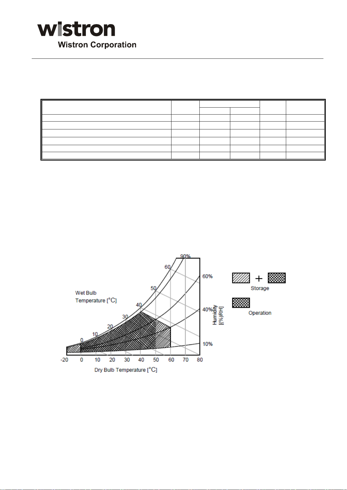
2. Temperature and relative humidity range are shown in the figure below. Wet bulb temperature
should be Max 39 °C and no condensation of water.
3. Gravity mura can be guaranteed below 40℃condition.
4. The maximum operating temperature is based on the test condition that the surface temperature
of display area is less than or equal to 68 ℃with LCD module alone in a temperature controlled
chamber. Thermal management should be considered in final product design to prevent the surface
temperature of display area from being over 68 ℃. The range of operating temperature may
degrade in case of improper thermal management in final product design.
All Copyright Reserved by Wistron Corporation Page 5 / 28
Page 6
V470FWSS02 Specification
(Preliminary Rev 0.4)
Item
Symbol
Value
Unit
Note
Min.
Typ.
Max.
Power Input Voltage
V
LCD
10.8
12.0
13.2
V
Power Input Current
I
LCD
501
626
mA 1
717
897
mA
2
Power Consumption
P
LCD
6.01
8.26
Watt 1 Rush current
I
Rush
5.0 A 3
3 Electrical characteristics
3.1 OPEN CELL
Note:
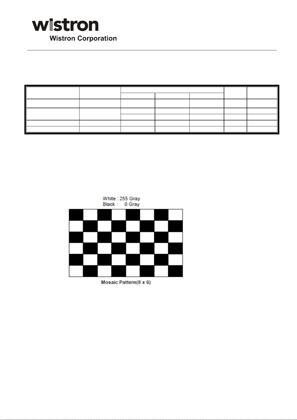
1. The specified current and power consumption are under the VLCD=12.0V, Ta=25±2°C, fV=60Hz
condition, and mosaic pattern(8 x 6) is displayed and fV is the frame frequency.
2. The current is specified at the maximum current pattern.
3. The duration of rush current is about 2ms and rising time of power input is 0.5ms (min.).
4. Ripple voltage level is recommended under ±5% of typical voltage
All Copyright Reserved by Wistron Corporation Page 6 / 28
Page 7
V470FWSS02 Specification
(Preliminary Rev 0.4)
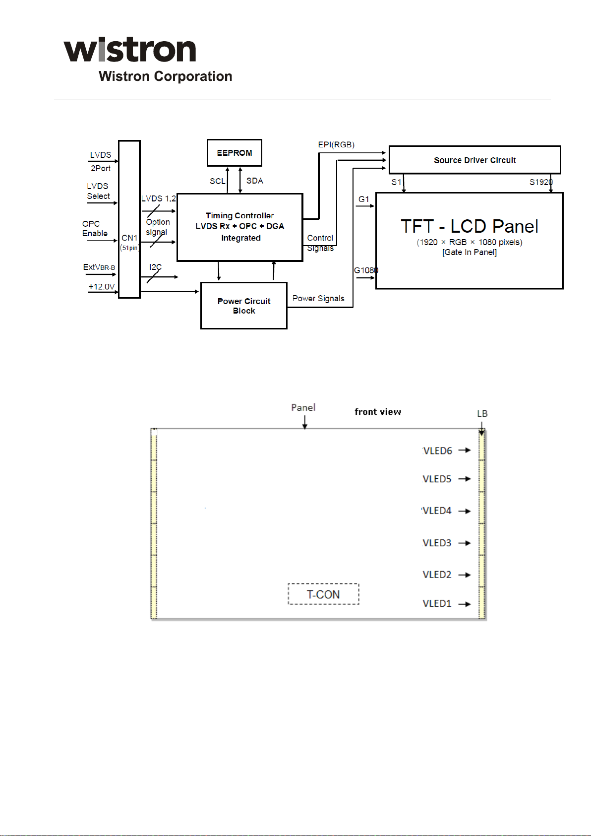
3.2 BACKLIGHT UNIT
The back light unit contains Edge type white LEDs (Ta=25±2℃) (Front view)
All Copyright Reserved by Wistron Corporation Page 7 / 28
Page 8
V470FWSS02 Specification
(Preliminary Rev 0.4)
Parameter
Symbol
Value
Unit
Note
Min.
Typ.
Max.
LED Light Bar Input Voltage Per
Input Pin
VPIN
72.6
78.7
V
(1)
Duty=100%,
IPIN=130mA
LED Light Bar Current Per Input Pin
IPIN
-
130
136
mA
(1), (2)
Duty=100%
String to String Δ Vf
Δ Vf
2.2 V IPIN=130mA
LED Life Time
LLED
30000 - -
Hrs
(3)
Power Consumption
(No Scanning)
PBL
56.3
W
(1)
Duty=100%,
IPIN=130mA
LB Spec:
CN of LB to DB cable type : A2008H00-8P
Note
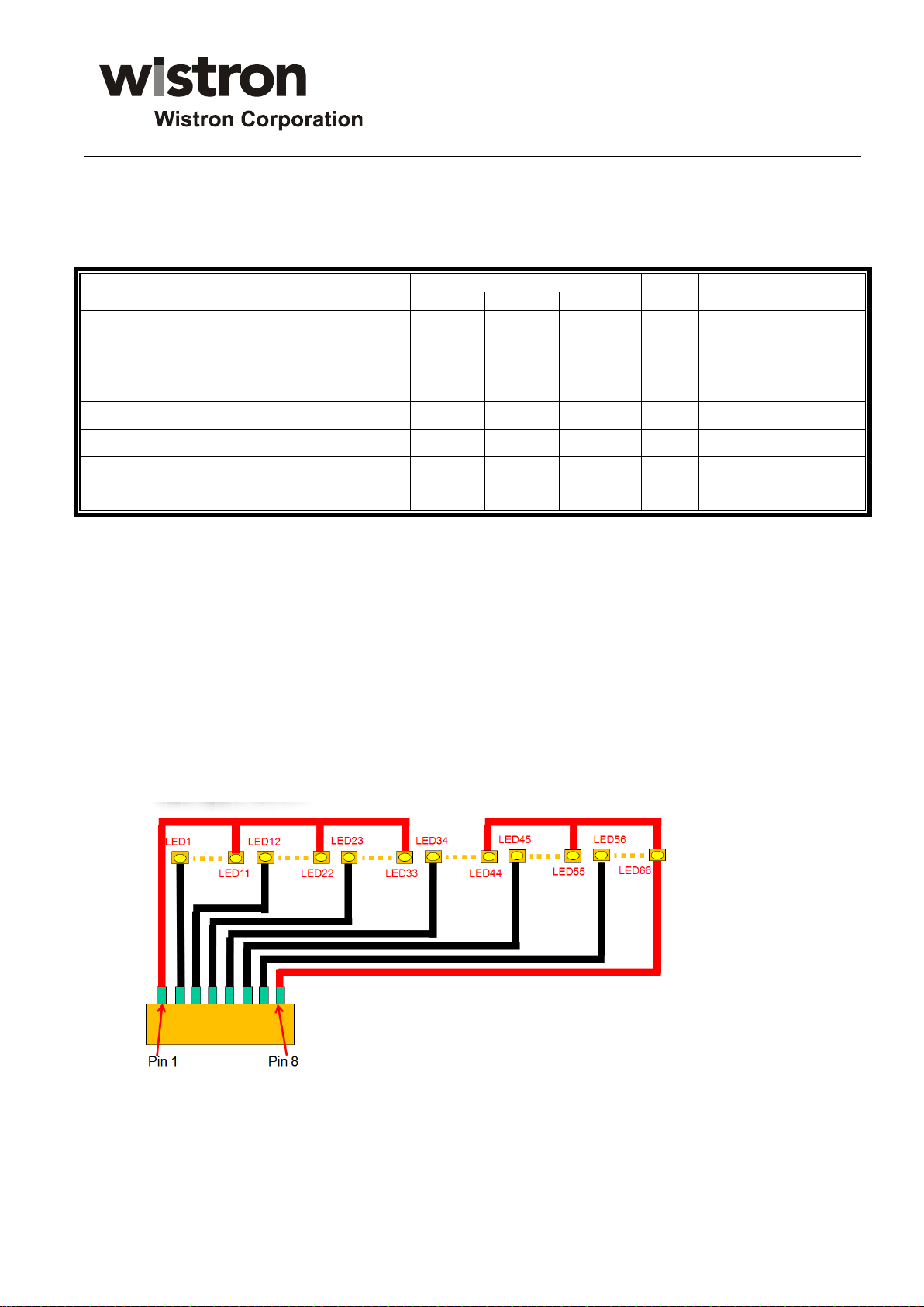
(1) LED light bar input voltage and current are measured by utilizing a true RMS multimeter as shown below
(2) PBL = I
(3) The lifetime of LED is defined as the time when LED packages continue to operate under the conditions
at Ta = 25 ±2 ℃ and I= (130)mA (per chip) until the brightness becomes ≦ 50% of its original value
(4) Permanent damage to the device may occur if maximum values are exceeded. Function operation
should be restricted to the conditions described under Normal Operating Conditions.
(5) Specified values are for input pin of LED light bar at Ta=25±2 ℃
PIN
× V
× 6 (String) , LED light bar circuit is (11)Series, (6) String.
PIN
All Copyright Reserved by Wistron Corporation Page 8 / 28
Page 9
V470FWSS02 Specification
(Preliminary Rev 0.4)
PIN
Name
Description
PIN
Name
Description
1
NC or GND
No Connection or Ground
26
NC or GND
No Connection or Ground
2
NC
No Connection (Note 4)
27
NC
No Connection
3
NC
No Connection (Note 4)
28
R2AN
2nd LVDS signal A-
4
NC
No Connection
29
R2AP
2nd LVDS signal A+
5
NC
No Connection
30
R2BN
2nd LVDS signal B-
6
NC
No Connection
31
R2BP
2nd LVDS signal B+
7
LVDS
Select
H=JEIDA, L or NC=VESA
32
R2CN
2nd LVDS signal C-
8
NC
No Connection (Note 4)
33
R2CP
2nd LVDS signal C+
9
NC
No Connection (Note 4)
34
GND
Ground
10
NC
No Connection (Note 4)
35
R2CLKN
2nd LVDS clock signal(-)
11
GND
Ground
36
R2CLKP
2nd LVDS clock signal(+)
12
R1AN
1st LVDS signal A-
37
GND
Ground
13
R1AP
1st LVDS signal A+
38
R2DN
2nd LVDS signal D-
14
R1BN
1st LVDS signal B-
39
R2DP
2nd LVDS signal D+
15
R1BP
1st LVDS signal B+
40
NC
No Connection
16
R1CN
1st LVDS signal C-
41
NC
No Connection
17
R1CP
1st LVDS signal C+
42
NC or GND
No Connection or Ground
18
GND
Ground
43
NC or GND
No Connection or Ground
19
R1CLKN
1st LVDS clock signal(-)
44
GND
Ground
20
R1CLKP
1st LVDS clock signal(+)
45
GND
Ground
21
GND
Ground
46
GND
Ground
22
R1DN
1st LVDS signal D-
47
NC
No Connection
23
R1DP
1st LVDS signal D+
48
VLCD
Power Supply +12V
24
NC
No Connection
49
VLCD
Power Supply +12V
25
NC
No Connection
50
VLCD
Power Supply +12V
51
VLCD
Power Supply +12V
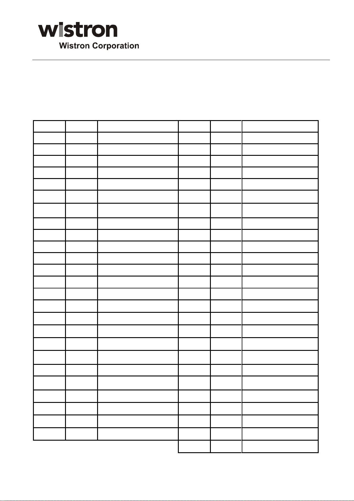
3.3 INPUT TERMINAL PIN ASSIGNMENT
- LCD Connector (CN1): FI-RES51S-HF (manufactured by JAE)
- Mating Connector: FI-R51HL (JAE) or compatible
3.3.1 LVDS PIN ASSIGNMEN(51-pin) Connector: FI-RE51S-HF(JAE) or compatible
All Copyright Reserved by Wistron Corporation Page 9 / 28
Page 10
V470FWSS02 Specification
(Preliminary Rev 0.4)
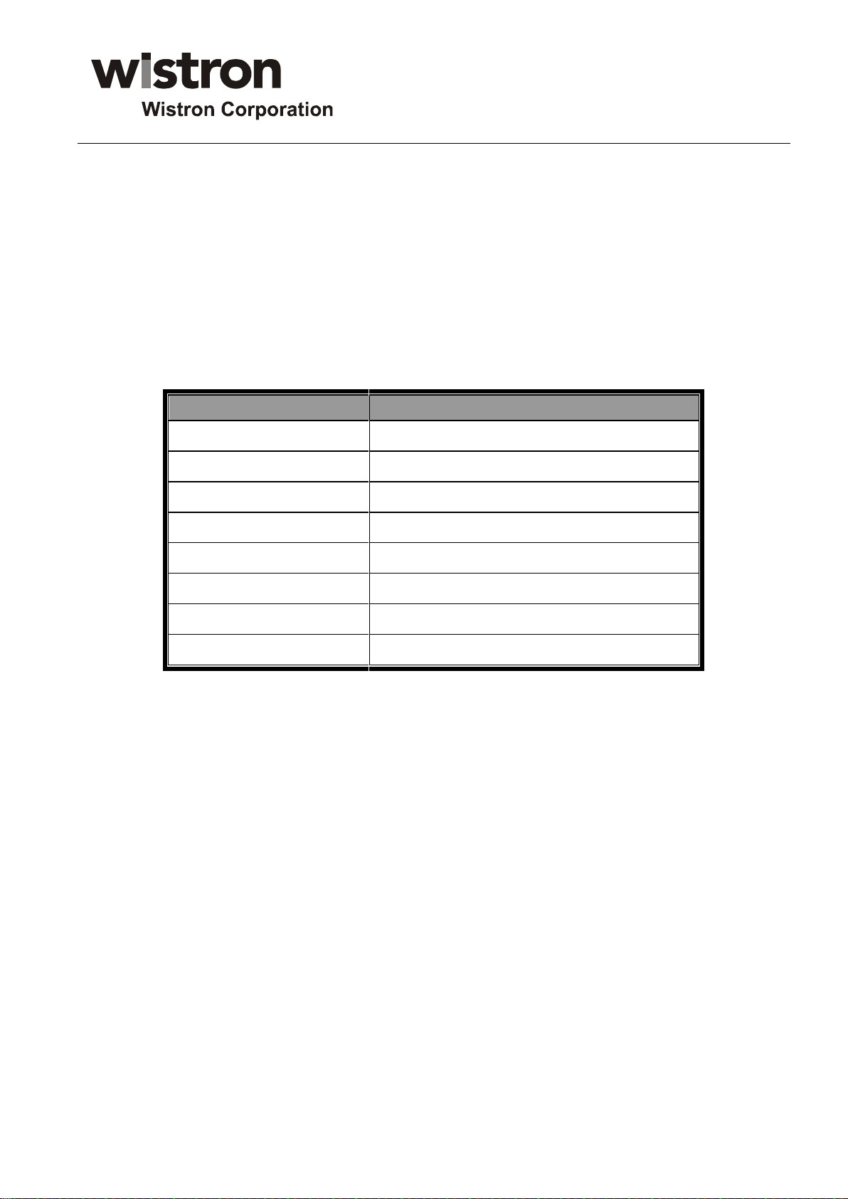
Pin number
Description
Pin 1
VIN
Pin 2
LVLED1
Pin 3
LVLED2
Pin 4
LVLED3
Pin 5
LVLED4
Pin 6
LVLED5
Pin 7
LVLED6
Pin 8
VIN
Note
1. All GND (ground) pins should be connected together to the LCD module’s metal frame.
2. All V
3. All input levels of LVDS signals are based on the EIA 644 Standard.
4. #1~#6 & #8~#10 NC (No Connection): These pins are used only for LGD (do not connect)
5. Specific pin No. #44 is used for “No signal detection “ of system signal interface. It should be GND for NSB (No
Signal Black) during the system interface signal is not. If this pin is “H” ,LCD Module displays AGP (Auto
Generation Pattern).
(power input) pins should be connected together.
LCD
3.3.2 Backlight LB connector Pin Assignment
Connector Part NO. : A2008H00-8P or Equivalent
All Copyright Reserved by Wistron Corporation Page 10 / 28
Page 11
V470FWSS02 Specification
(Preliminary Rev 0.4)
Item
Symbol
Min
Typ
Max
Unit
Note
Frequency
DCLK
fCLK
63.00
74.25
78.00
MHz - Hsync
FH
57.3
67.5
70
KHz
-
Vsync
FV
57
(47)
60
(50)
63
(53)
Hz 2 NTSC
(PAL)
Vertical
Display Period
TVV
1080
1080
1080-
Lines
-
Blank
tVB
20
(228)
45
(270)
69
(300)
Lines
1
Vertical
Total
TVP
1100
(1308)
1125
(1350)
1149
(1380)
Lines
-
Horizontal
Display Period
THV
960
960
960-
tCLK
1920/2-
Blank
tHB
100
140
240
tCLK
1
Horizontal
Total
THP
1060
1100
1200
tCLK
-
3.4 Signal Timing Specifications
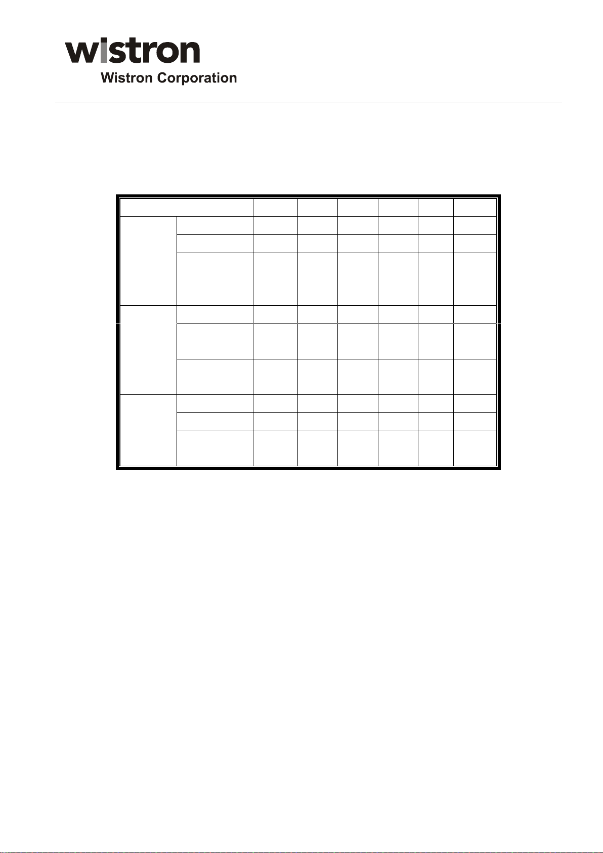
Below table shows the signal timing required at the input of the LVDS transmitter. All of the interface signal
timings should be satisfied with the following specification for normal operation.
Note:
1. The input of HSYNC & VSYNC signal does not have an effect on normal operation (DE Only Mode).
2. The performance of the electro-optical characteristics may be influenced by variance of the vertical
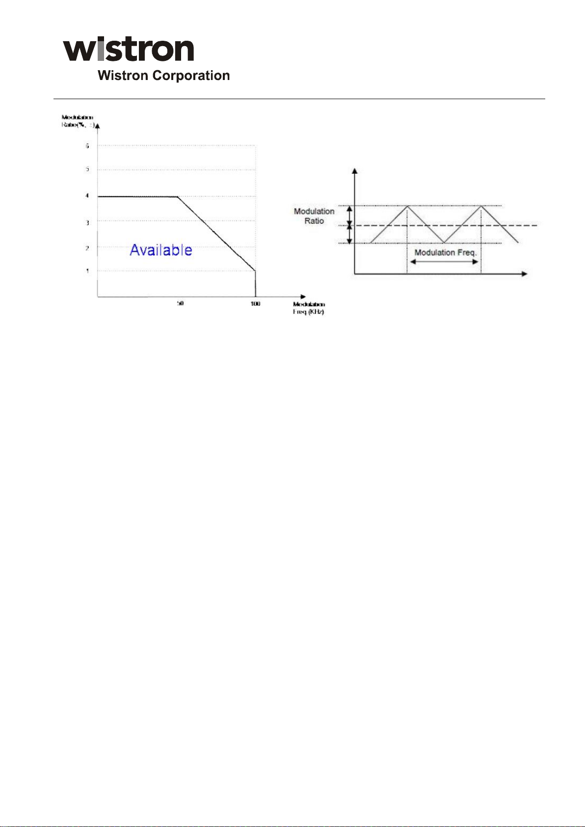
3. Spread Spectrum Rate (SSR) for 50KHz~ 100kHz Modulation Frequency (FMOD) is calculated by
(7- 0.06*Fmod), where Modulation Frequency (FMOD) unit is KHz.
If you use spread spectrum of EMI, add some additional clock to minimum value for clock margin.
refresh rate and the horizontal frequency
LVDS Receiver Spread spectrum Clock is defined as below figure.
※Timing should be based on clock frequency.
All Copyright Reserved by Wistron Corporation Page 11 / 28
Page 12
V470FWSS02 Specification
(Preliminary Rev 0.4)
※ Please pay attention to the followings when you set Spread Spectrum Rate (SSR) and Modulation
Frequency (FMOD)
1. Please set proper Spread Spectrum Rate (SSR) and Modulation Frequency (FMOD) of TV system
LVDS output.
2. Please check FOS after you set Spread Spectrum Rate (SSR) and Modulation Frequency (FMOD) to
avoid abnormal display. Especially, harmonic noise can appear when you use Spread Spectrum under
FMOD 30KHz.
All Copyright Reserved by Wistron Corporation Page 12 / 28
Page 13
V470FWSS02 Specification
(Preliminary Rev 0.4)
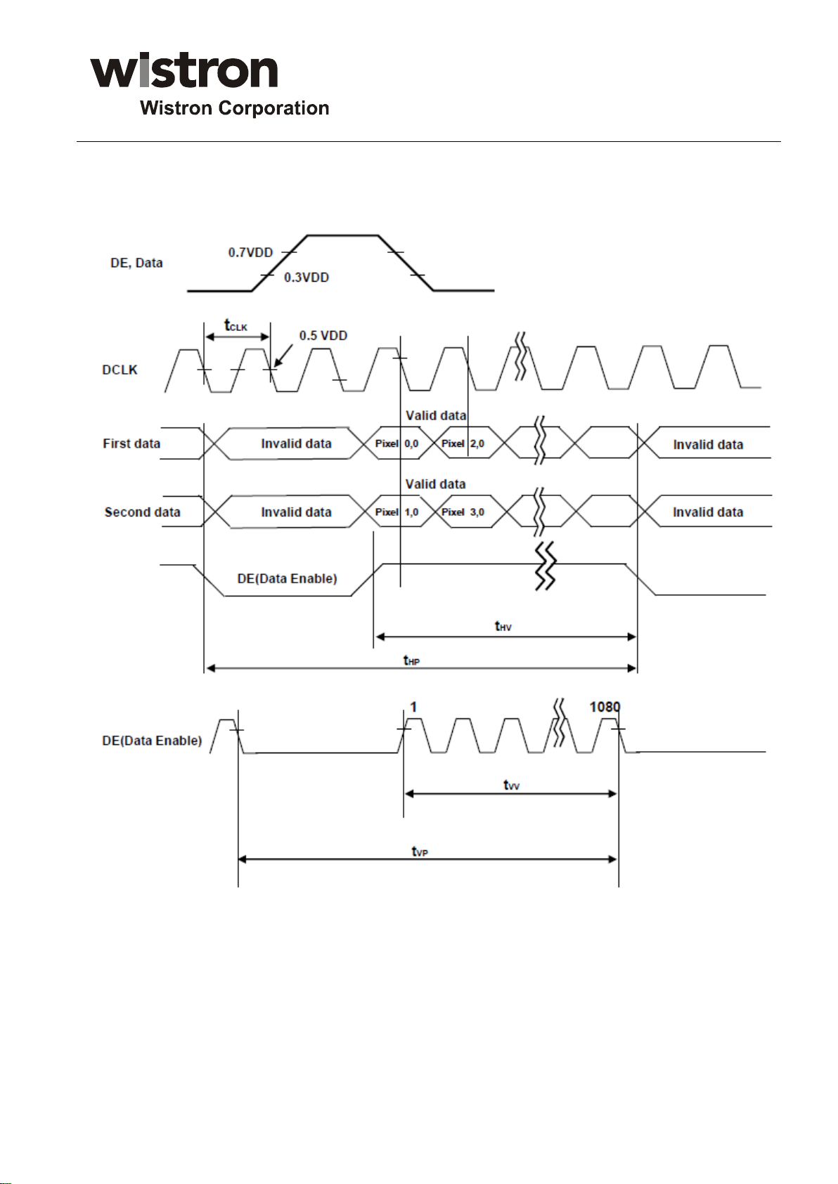
3.5 LVDS Signal Specification
3-5-1. LVDS Input Signal Timing Diagram
All Copyright Reserved by Wistron Corporation Page 13 / 28
Page 14
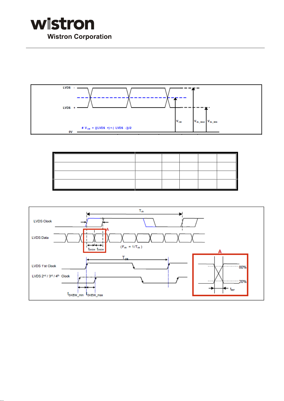
V470FWSS02 Specification
(Preliminary Rev 0.4)
Description
Symbol
Min
Max
Unit
Note
LVDS Common mode Voltage
VCM
1.0
1.5 V
LVDS Input Voltage Range
VIN
0.7
1.8 V
Change in common mode Voltage
Δ VCM
-
250
mV
3-5-2. LVDS Input Signal Characteristics
3-5-2-1 DC Specification
3-5-2-2 AC Specification
All Copyright Reserved by Wistron Corporation Page 14 / 28
Page 15
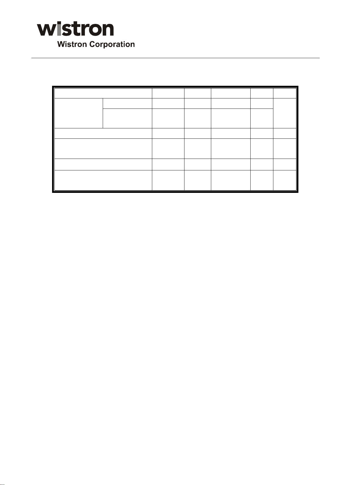
V470FWSS02 Specification
(Preliminary Rev 0.4)
Description
Symbol
Min
Max
Unit
Note
LVDS
Differential
Voltage
High Threshold
VTH
100
300
mV
3
Low Threshold
VTL
-300
-100
mV
LVDS Clock to Data Skew
t
SKEW
-
|(0.20*T
clk
)/7|
ps
-
LVDS Clock/Data Rising/Falling
time
tRF
260-
|(0.3*T
clk
)/7|
ps
2
Effective time of LVDS
t
eff
|±360|
-
ps
-
LVDS Clock to Clock Skew (Even to
Odd)
t
SKEW_EO
-
|1/7*T
clk
|
ps
-
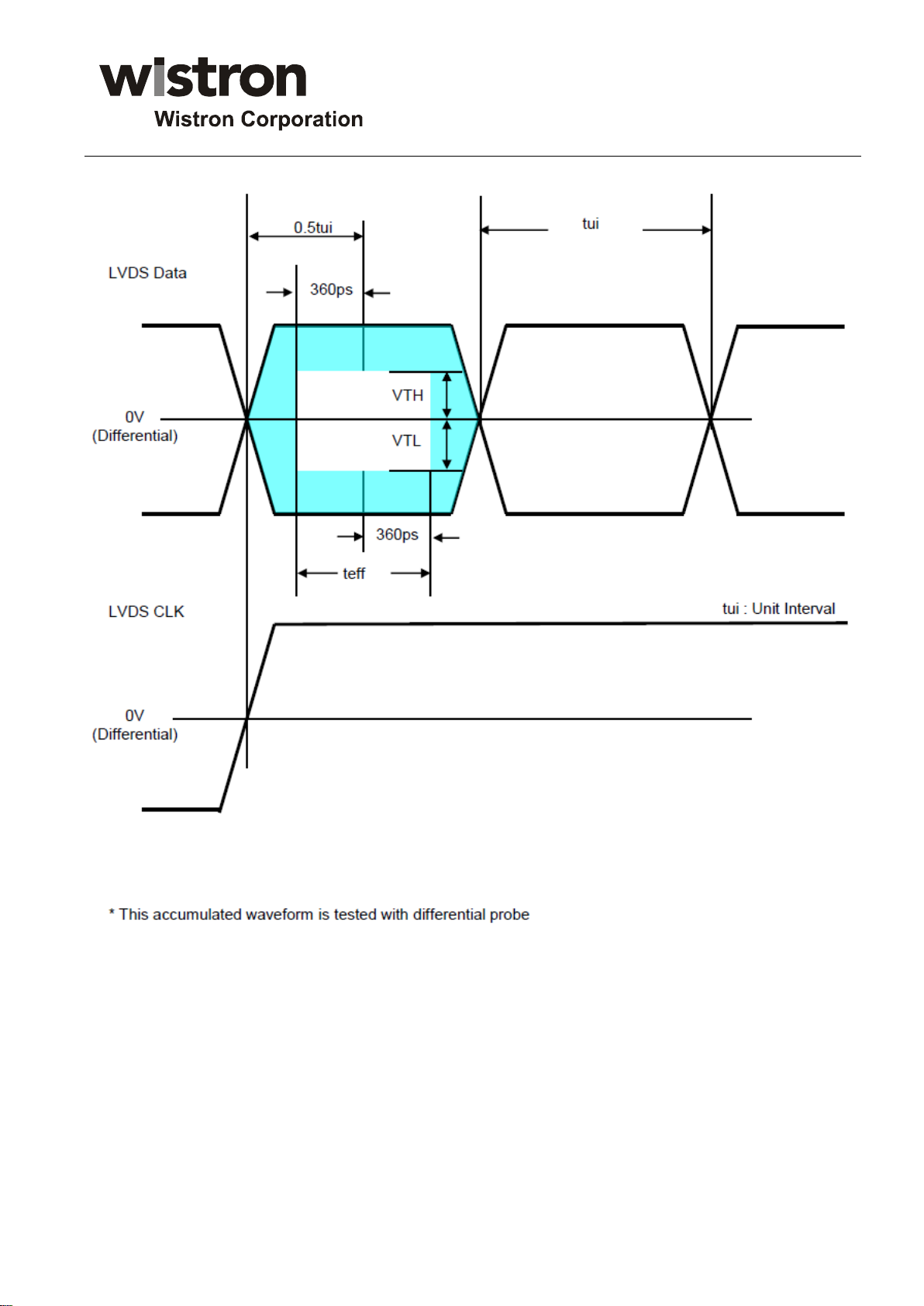
Note 1. All Input levels of LVDS signals are based on the EIA 644 Standard.
2. If tRF isn’t enough, t
3. LVDS Differential Voltage is defined within t
should be meet the range.
eff
eff
All Copyright Reserved by Wistron Corporation Page 15 / 28
Page 16
V470FWSS02 Specification
(Preliminary Rev 0.4)
All Copyright Reserved by Wistron Corporation Page 16 / 28
Page 17
V470FWSS02 Specification
(Preliminary Rev 0.4)
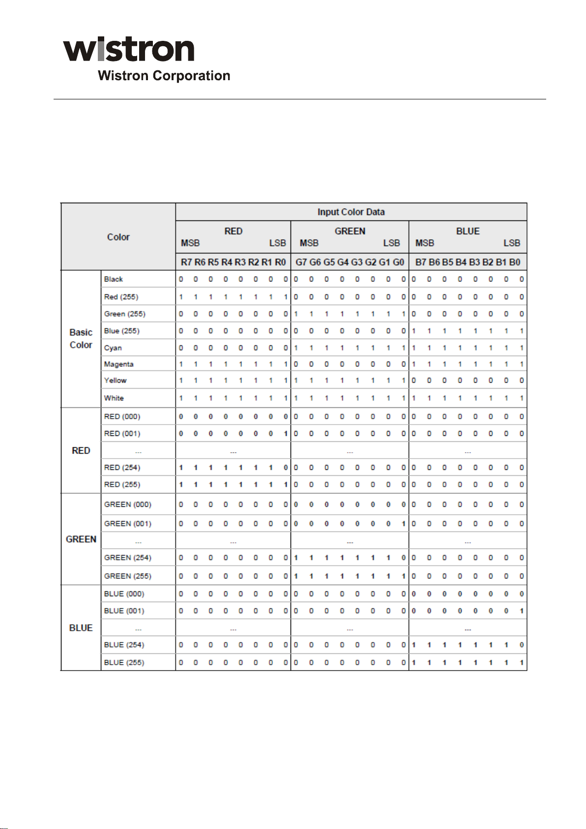
3-6. Color Data Reference
The brightness of each primary color (red, green, blue) is based on the 10bit gray scale data input for the color.
The higher binary input, the brighter the color. Below table provides a reference for color versus data input.
COLOR DATA REFERENCE
All Copyright Reserved by Wistron Corporation Page 17 / 28
Page 18
V470FWSS02 Specification
(Preliminary Rev 0.4)
Parameter
Value
Unit
Notes
Min
Typ
Max
T1
0.5
-
20
ms
1
T2
0 -
ms
2
T3
400 -
ms
3
T4
200 -
ms
3
T5
1.0 - s 4
T6
0 - T2
ms
5
T7
0 -
ms
6
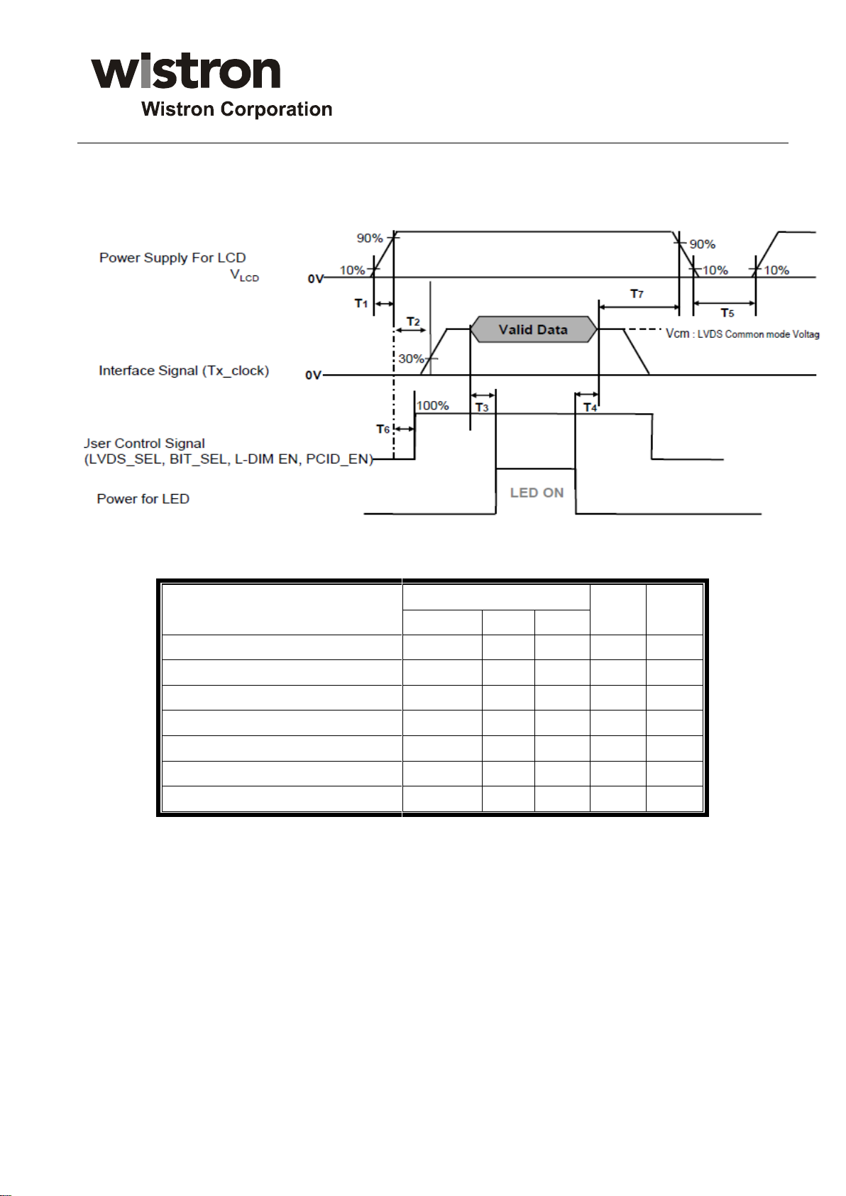
3-7. Power Sequence
3-7-1. LCD Driving circuit
Table 1.
Note:
1. Even though T1 is over the specified value, there is no problem if I2T spec of fuse is satisfied.
2.If T2 is satisfied with specification after removing LVDS Cable, there is no problem.
3.The T3/T4 is recommended value, the case when failed to meet a minimum specification, abnormal
display would be shown. There is no reliability problem.
4.T5 should be measured after the Module has been fully discharged between power off and on
period.
5.If the on time of signals (Interface signal and user control signals) precedes the on time of Power
(V
), it will be happened abnormal display. When T6 is NC status,T6 doesn’t need to be measured.
LCD
6.It is recommendation specification that T7 has to be 0ms as a minimum value.
※Please avoid floating state of interface signal at invalid period.
※When the power supply for LCD (VLCD) is off, be sure to pull down the valid and invalid data to 0V.
All Copyright Reserved by Wistron Corporation Page 18 / 28
Page 19
V470FWSS02 Specification
(Preliminary Rev 0.4)
Item
Symbol
Value
Unit
Ambient Temperature
Ta
25±2
C
Ambient Humidity
Ha
50±10
%RH
Supply Voltage
Vpin
72.6
V
Input Signal
According to typical value in "3.
ELECTRICAL CHARACTERISTICS"
LED Light Bar Input Current (Per Input Pin)
IPIN
130
mADC
PWM Duty Ratio
D
100
%
LED Light Bar Test Converter
By OBD define
Item
Symbol
Condition
Value
Unit
Note
Min
Typ
Max
Color
Chromaticity
(CIE 1931)
Red
Rx
x
=
Y
CS-2000A
Typ
-0.03
0.65
Typ+0.03
-
(1) (5)
Ry
0.335
Green
Gx
0.315
Gy
0.605
Blue
Bx
0.15
By
0.059
White
Wx
0.255
0.285
0.315
Wy
0.272
0.302
0.332
Center Luminance of White (Center
of Screen)
Lc 350 - -
(4) (5)
Contrast Ratio
CR
1000
1400 -
(2) (5)
Color Gamut
NTSC
72 - %
Response
Time
Variation
G to Gσ
6 9 G-to-G (BW)
G-to-G
(BW)
-
-
8
12
ms
(3)
White Variation (9P)
δw
θ
x
θ
Y
=0°
CS-2000A
75 - %
(5) (6)
Viewing
Angle
2D
(CR>10)
Horizontal
θ
x +
CR≧10
CS-2000A
89 - -
Deg.
(1),(5)
θ
x -
89 - -
Vertical
θ
y +
89 - -
θ
y -
89 - -
3D
(CT≦
10%)
Vertical
θ
y+
+ θ
y -
CT≦10%
16
20
Deg.
(8)
3D Crosstalk
3D C/T 1 3
%
(8)
Gray Scale
- - -
(9)
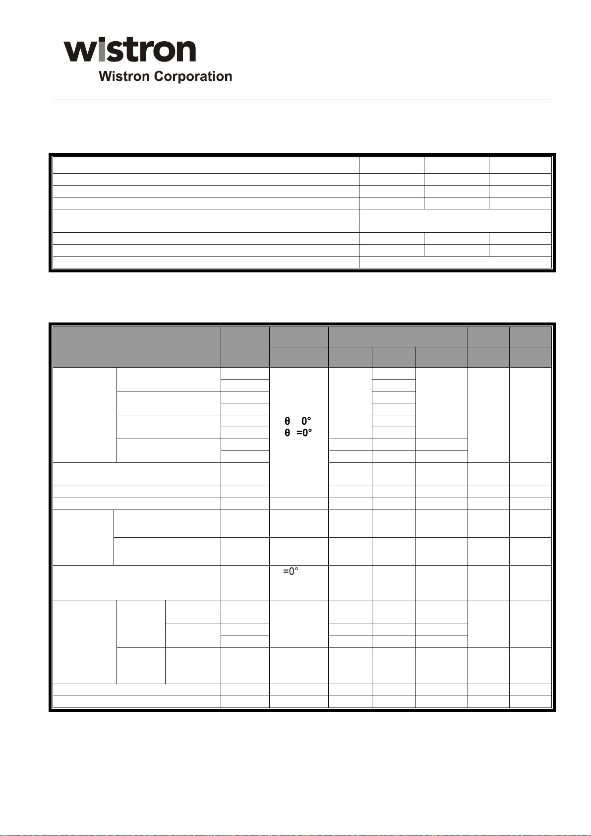
4 OPTICAL CHARACTERISTICS
4.1 TEST CONDITIONS
4.2 OPTICAL SPECIFICATIONS
The relative measurement methods of optical characteristics are shown as below. The following items should be
measured under the test conditions described in 4.1 and stable environment shown in Note (5).
All Copyright Reserved by Wistron Corporation Page 19 / 28
Page 20
V470FWSS02 Specification
(Preliminary Rev 0.4)
Note
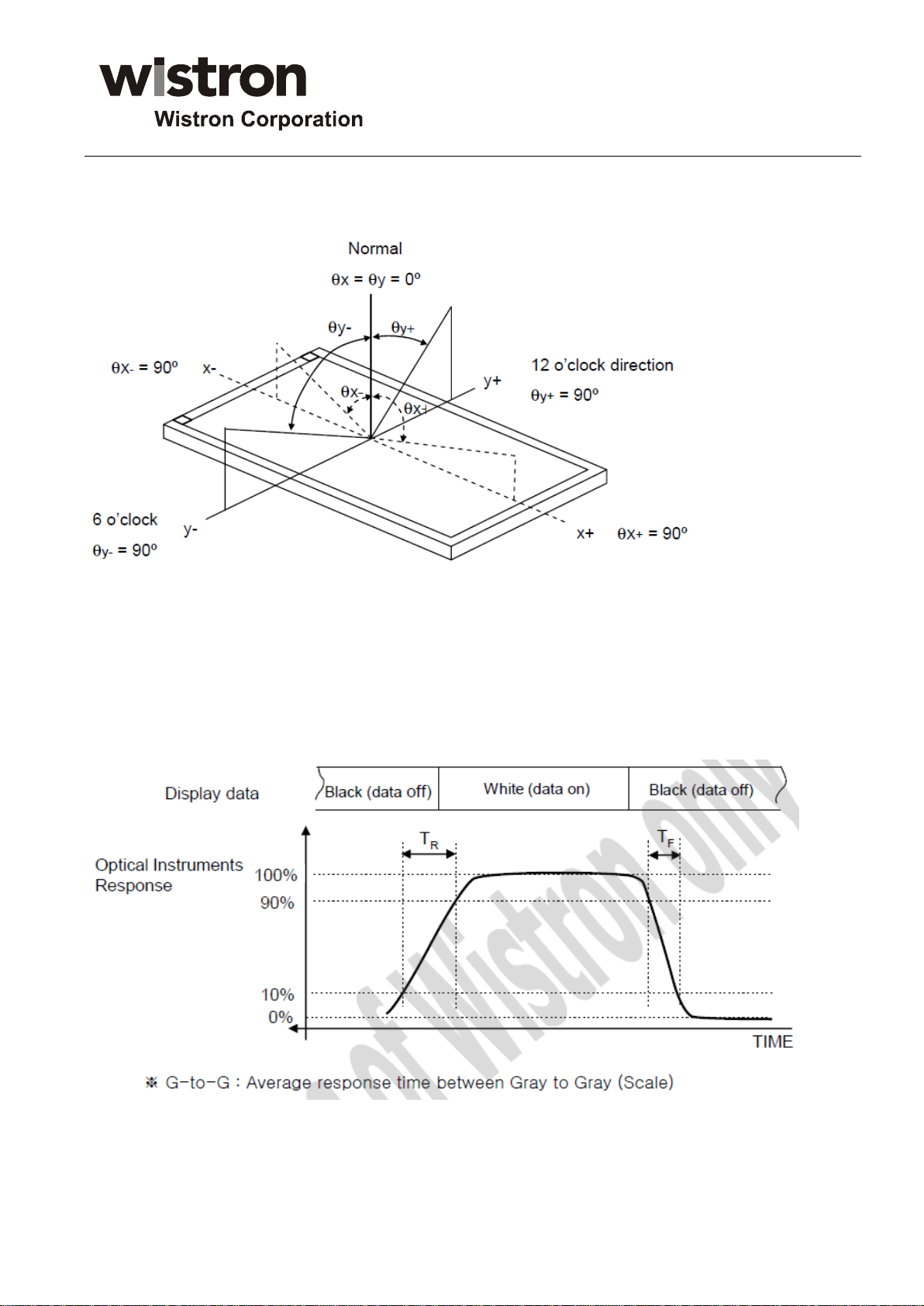
(1) Definition of Viewing Angle (θx, θy):
(2) Definition of Contrast Ratio (CR):
The contrast ratio can be calculated by the following expression.
Contrast Ratio (CR) = L255 / L0
L255: Luminance of gray level 255
L 0: Luminance of gray level 0
CR = CR (1)
CR (X) is corresponding to the Contrast Ratio of the point X at Figure in Note (6).
(3) Definition of Response Time : Sum of TR, TF
All Copyright Reserved by Wistron Corporation Page 20 / 28
Page 21
V470FWSS02 Specification
(Preliminary Rev 0.4)
W/6
W/2
W
W/6
H/6
H/2
H
Horizontal Line
Vertical Line
H/6
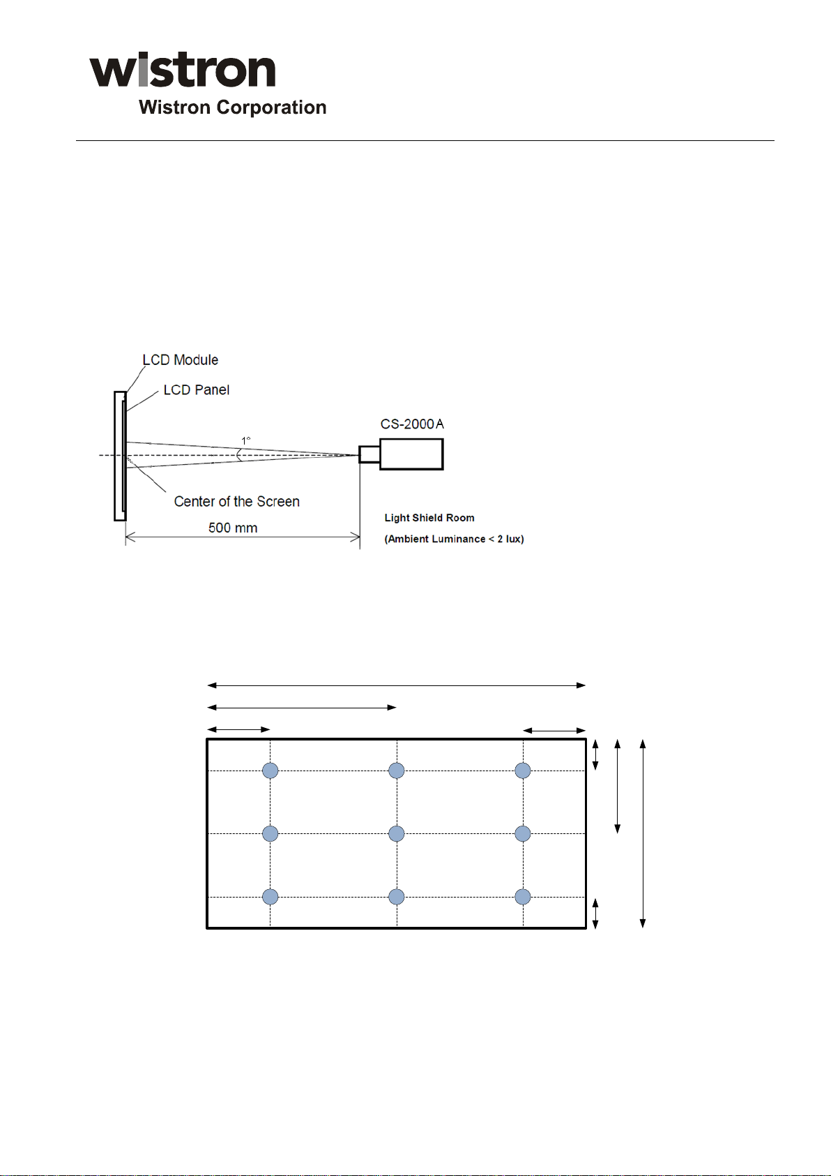
(4) Definition of Luminance of White (LC):
Measure the luminance of gray level 255 at center point
LC = L (1)
L (x) is corresponding to the luminance of the point X at Figure in Note (6).
(5) Measurement Setup:
The LCD module should be stabilized at given temperature for 20 minutes to avoid abrupt temperature change
during measuring. In order to stabilize the luminance, the measurement should be executed after lighting
backlight for 20 minutes in a windless room
(6)Definition of white variation (δW):
Measure the luminance of gray level 255 at 9 points
δW = Maximum [L (1), L (2) ……L (4), L (9)] / Minimum [L (1), L (2) …… L (4), L (9)]
All Copyright Reserved by Wistron Corporation Page 21 / 28
Page 22
V470FWSS02 Specification
(Preliminary Rev 0.4)
(7)G to Gσ is Variation of Gray to Gray response time composing a picture
G to G(σ) = √(Σ (Xi-u)2/N); Xi = Individual Data, u = Data average, N: The number of Data
(8) 3D performance specification is expressed by 3D luminance and 3D viewing angle.
(9) Gray scale specification
Gamma Value is approximately 2.2. For more information , see the Table 1.
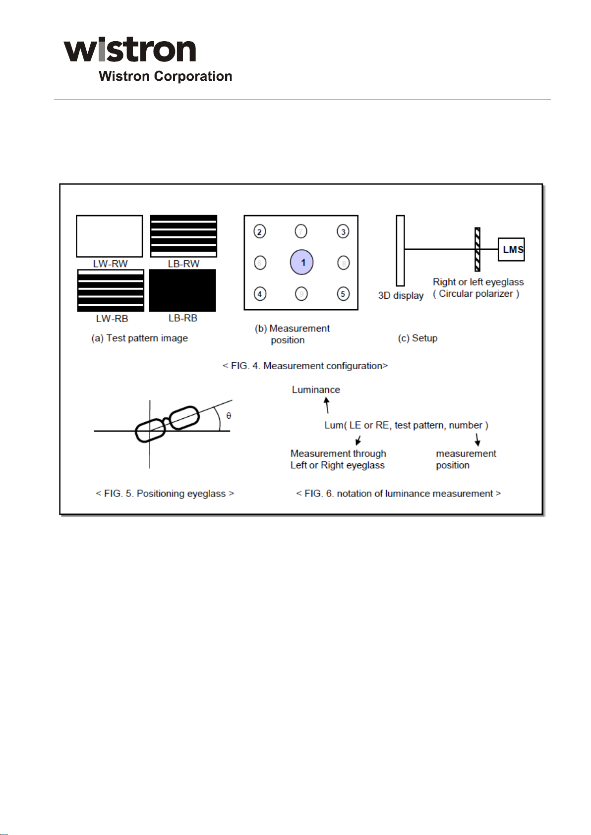
In order to measure 3D luminance, 3D crosstalk and 3D viewing angle, it need to be prepared as below;
1) Measurement configuration
4-Test pattern images. Refer to FIG4.
-. LW-RW: White for left and right eye
-. LW-RB: White for left eye and Black for right eye
-. LB-RW: Black for left eye and white for right eye
-. LB-RB: Black for left eye and right eye
Image files where black and white lines are displayed on even or odd lines.
Luminance measurement system (LMS) with narrow FOV (files of view) is used.
2) Positioning Eyeglass (refer to appendix-VII for standard specification of eyeglass)
(i) Test image (LB-RW) is displayed.
(ii) Left eyeglass are placed in front of LMS and luminance is measured,
Rotating right eyeglass such as FIG5. The rotation for luminance measurement is “LUM(LE, LB-RW,1)”.
(ii) Find the angle where luminance is minimum.
*Following measurements should be performed at the angle of minimum transmittance of eyeglass.
3) Measurement of 3D luminance
(i) Test image (LW-RW) is displayed.
(ii) Left or right eyeglass are placed in front of LMS successively and
Luminance is measured at center 1 point where the notation for luminance measurement is
“Lum(LE,LW-RW,1)” or “Lum(RE, LW-RW, 1).
All Copyright Reserved by Wistron Corporation Page 22 / 28
Page 23
V470FWSS02 Specification
(Preliminary Rev 0.4)
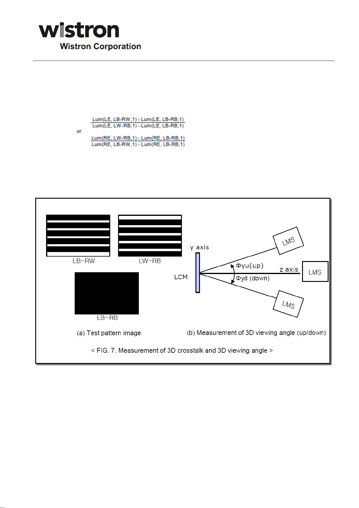
4) Measurement of 3D crosstalk
(i) Test image (LB-RW, LW-RB and LB-RB) is displayed.
(ii) Right or left eyeglass are placed in front of LMS successively and
luminance is measured for position 1.
with rotation LMS or sample vertically.
5) Measurement of 3D Viewing Angle
3D viewing angle is the angle at which the 3D crosstalk is under 10%. The angles are
Determined for the vertical or y axis with respect to the z axis which is normal to the LCD
Module surface and measured for position 1. For more information, see the Fig7
All Copyright Reserved by Wistron Corporation Page 23 / 28
Page 24
V470FWSS02 Specification
(Preliminary Rev 0.4)
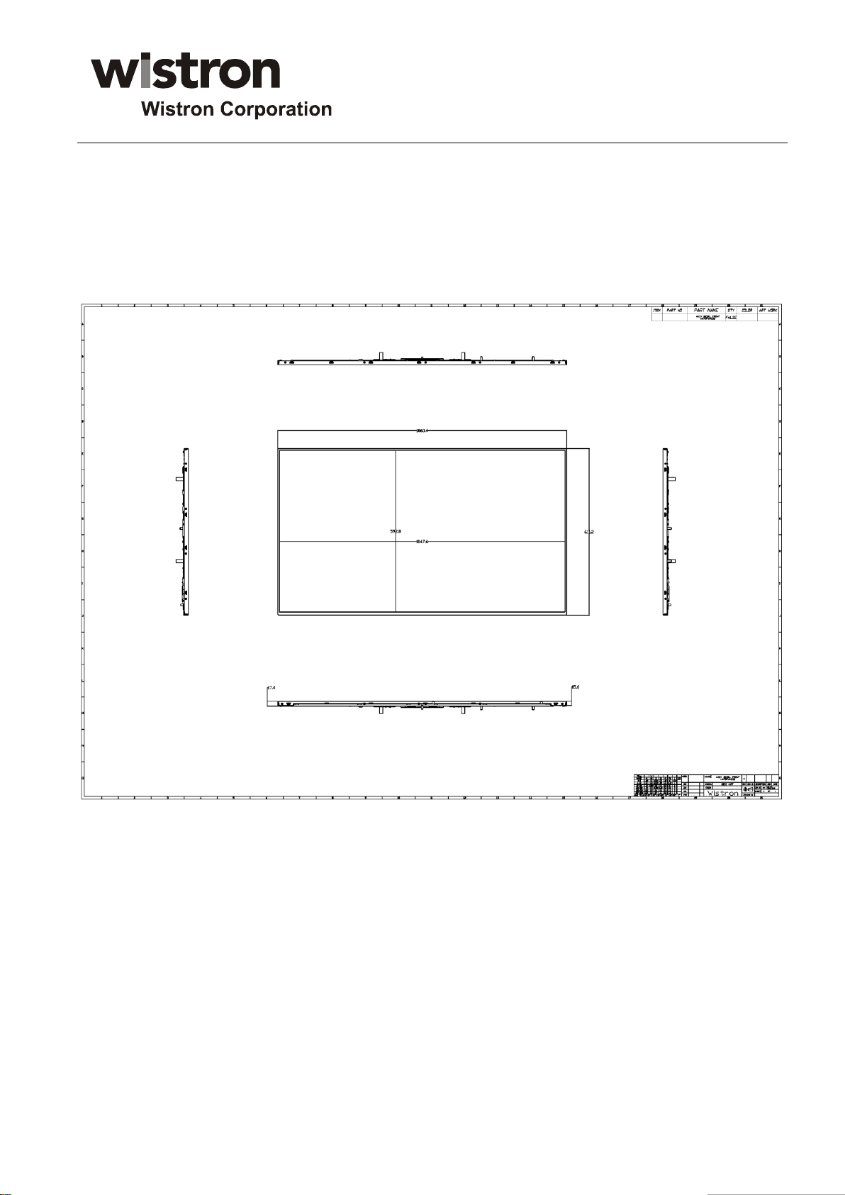
5 MECHANICAL CHARACTERISTICS
5.1 FRONT SIDE (W/O SYSTEM COVER)
All Copyright Reserved by Wistron Corporation Page 24 / 28
Page 25
V470FWSS02 Specification
(Preliminary Rev 0.4)
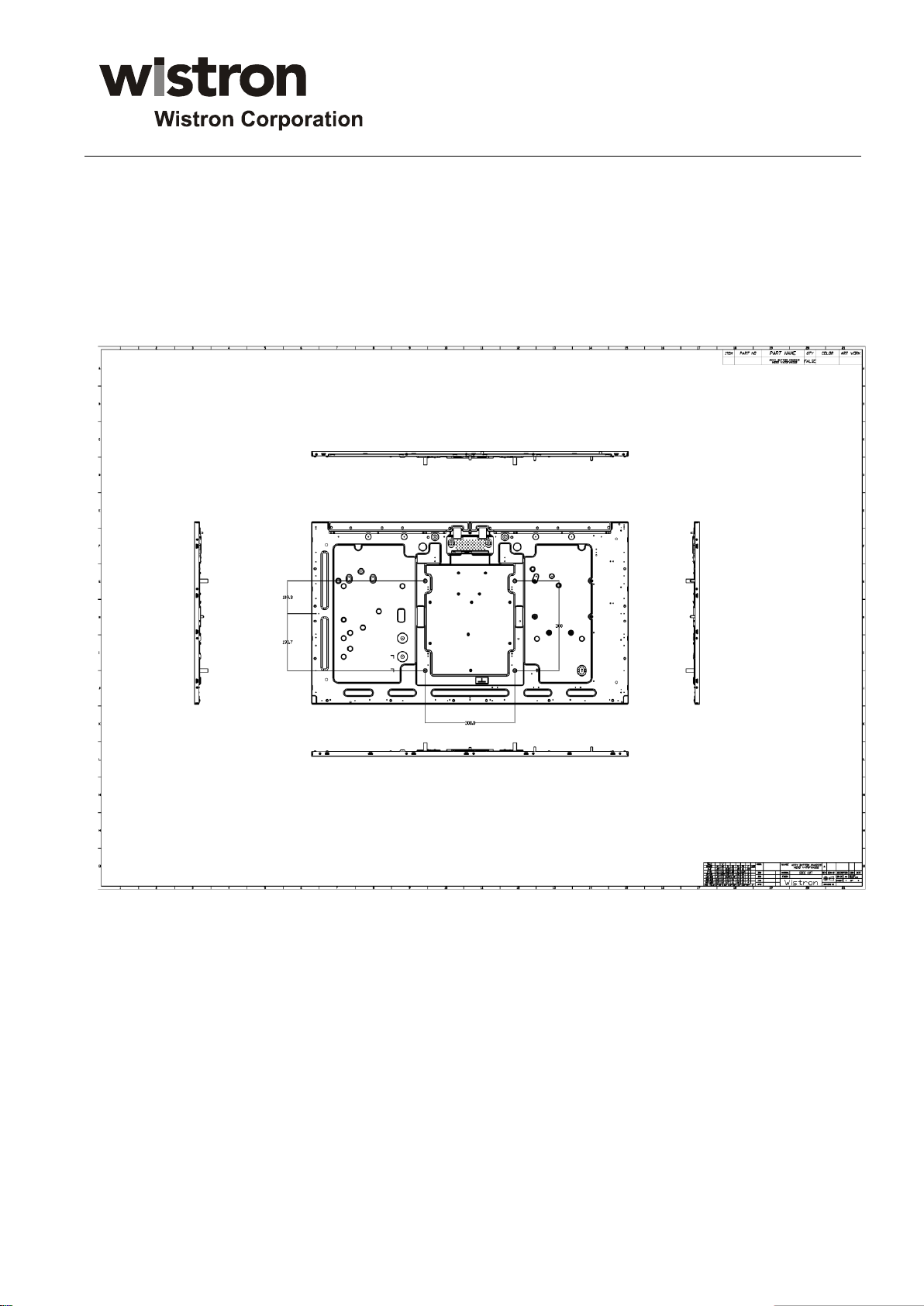
5.2 BACK SIDE
All Copyright Reserved by Wistron Corporation Page 25 / 28
Page 26
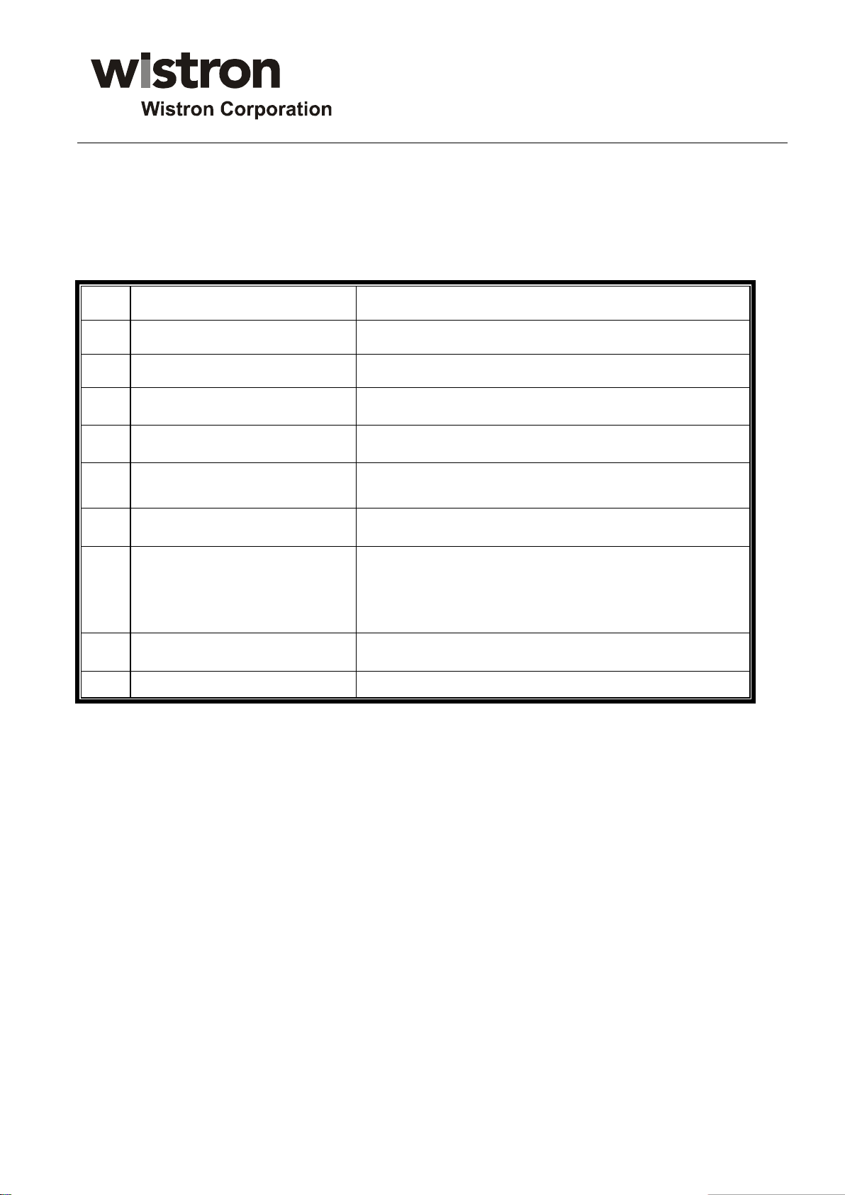
V470FWSS02 Specification
(Preliminary Rev 0.4)
No.
Items
Required Condition
1
High Temperature Operation Life
(HTOL)
Ta= 50℃ , 50%RH , 250hours
2
Low Temperature Operation Life
(LTOL)
Ta= 0℃ , 250hours
3
Low Temperature Storage (LTS)
Ta= -20oC, 250 hours
4
Wet High Temperature Storage
(WHTS)
40℃ , 90%RH, 250hours
5
Vibration Test (With TV packing)
5-50-5Hz (1cycle/3min), 19.8-0.2mm, 1G,
Up/Down 20cycles (other side 5cycles)
6
Drop Test (With TV packing)
Surface-60cm, Corner/Edge-48cm,
1 Corner/ 3 Edge/ 6 Surface
7
ESD (Electro Static Discharge)
. LCD Operation/Contact: ±8 kV, 1cm, 1 time/Point for metal
front bezel,330Ω/150pf
. LCD Operation/Air: ±12 kV, 1cm, 1 time/Point for the gap
between front bezel and open cell,330Ω/150pf
8
Pallet Vibration
Random wave/ 5~50Hz @ 0.021720 g2/Hz.Z axis,1H
9
Pallet Drop
28cm, Bottom flat two times
6 RELIABILITY TEST
Environment test conditions are listed as following table.
Note 1
This is front bezel integration design so that drop/vibration test could not be performed by individual panel
module. Please refer to TV set test result for this 2 tests.
All Copyright Reserved by Wistron Corporation Page 26 / 28
Page 27
V470FWSS02 Specification
(Preliminary Rev 0.4)
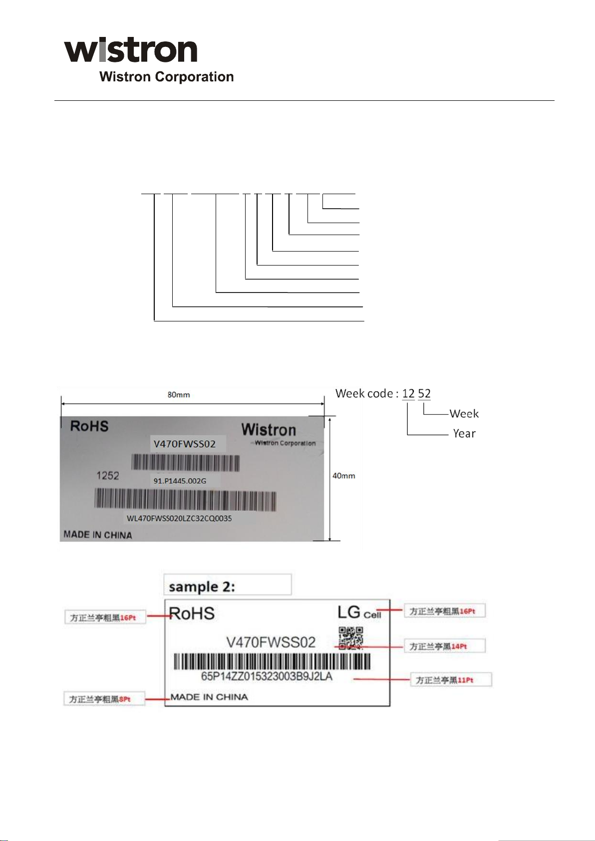
Serial Number
Year, Month, Day
Module Line
Module Location
Open Cell Vendor
Revision
Model Type Number
Size
Supplier Code
7 Labels
7.1 LABELS DEFINE
(1) LCM module Model Name : V470FWSS02
(2) LCM Part Number : NA
(3) Lot No. : XX XXX XXXXXX X X XX X XXX XXXX
SAMPLE:
All Copyright Reserved by Wistron Corporation Page 27 / 28
Page 28

V470FWSS02 Specification
(Preliminary Rev 0.4)
8 PRECAUTIONS
8.1 ASSEMBLY AND HANDLING PRECAUTIONS
(1) Do not apply rough force such as bending or twisting to the module during assembly.
(2) To assemble or install module into user’s system can be only in clean working areas. The dust
and oil may cause electrical short or worsen the polarizer.
(3) It’s not permitted to have pressure or impulse on the module because the LCD panel and
Backlight will be damaged.
(4) Always follow the correct power sequence when LCD module is connecting and operating. This
can prevent damage to the CMOS LSI chips during latch-up.
(5) Do not pull the I/F connector in or out while the module is operating.
(6) Do not disassemble the module.
(7) Use a soft dry cloth without chemicals for cleaning, because the surface of polarizer is very soft
and easily scratched.
(8) It is dangerous that moisture come into or contacted the LCD module, because moisture may
damage LCD module when it is operating.
(9) High temperature or humidity may reduce the performance of module. Please store LCD module
within the specified storage conditions.
(10) When ambient temperature is lower than 10ºC may reduce the display quality. For example, the
response time will become slowly.
8.2 SAFETY PRECAUTIONS
(1) Do not apply rough force such as bending or twisting to the module during assembly.
(2) To assemble or install module into user’s system can be only in clean working areas. The dust
and oil may cause electrical short or worsen the polarizer.
(3) After the module’s end of life, it is not harmful in case of normal operation and storage.
8.3 STORAGE
(1) Do not store the TFT – LCD module in direct sunlight
(2) The module should be stored in dark place. It is prohibited to apply sunlight or fluorescent light in
storing
(3) Do not leave the module in high temperature, and high humidity for a long time. It is highly
recommended to store the module with temperature from 0℃ to 35℃ And relative humidity of
less than 70%
8.4 OPERATION CONDITION GUIDE
(1) The LCD product should be operated under normal condition.
Normal condition is defined as below
Temperature : 20±15℃
Humidity: 65±20%
Display pattern : continually changing pattern(Not stationary)
(2) If the product will be used in extreme conditions such as high temperature, high humidity , high
altitude ,display pattern or operation time etc…It is strongly recommended to contact Wistron for
application engineering advice . Otherwise , Its reliability and function may not be guaranteed
8.5 OTHER
When fixed patterns are displayed for a long time, remnant image is likely to occur.
All Copyright Reserved by Wistron Corporation Page 28 / 28
 Loading...