

Page 1

Liquid Crystal Display Television
Service Manual
Chassis: MST6E16JS
Product Type:LCD32V88AM(2)&LCD32V88AM(3)
Ver 1.0
Hisense Electric Co.,Ltd.
November, 2011
Page 2

Contents
Contents................................................................................................................................................................- 2 -
Service Manual ....................................................................................................................................................- 3 -
1. Precautions and notices..............................................................................................................................- 3 -
1.1 WARNING ......................................................................................................................................- 4 -
1.2 NOTES ............................................................................................................................................- 7 -
2. Factory/Service OSD Menu and Adjustment...........................................................................................- 10 -
2.1 T o enter the Factory OSD Menu....................................................................................................- 10 -
2.2 Factory OSD Menu........................................................................................................................- 10 -
3. Software Upgrading.................................................................................................................................- 15 -
Before upgrading, read the following..................................................................................................- 15 -
3.1 Get ready for upgrading.................................................................................................................- 15 -
3.2 Upgrading with the ISP_TOOL4.0.9.............................................................................................- 25 -
3.3 USB Software upgrading...............................................................................................................- 29 -
4. Circuit instruction....................................................................................................................................- 34 -
4.1 Main board Power assign and block diagram................................................................................- 34 -
4.2 Image and signal process...............................................................................................................- 35 -
4.3 The main IC description ................................................................................................................- 42 -
4.4 Troubleshooting.............................................................................................................................- 50 -
5. Schematic circuit diagram.......................................................................................................................- 57 -
- 2 -
Page 3

Service Manual
1. Precautions and notices
BEFORE SERVICING THE LCD TV, READ THE SAFETY PRECAUTIONS IN
THIS MANUAL.
WHEN REPLACEMENT PARTS ARE REQUIRED, BE SURE TO USE
REPLACEMENT PARTS SPECIFIED BY THE MANUFACTURER.
Proper service and repair is important to the safe, reliable operation of all Hisense
Electric Co., Ltd Equipment. The service procedures recommended by Hisense and
described in this Service Guide are effective methods of performing service
operations. Some of these service operations require the use of tools specially
designed for the purpose. The special tools should be used when and as
recommended.
It is important to note that this manual contains various CAUTIONS and NOTICES
which should be carefully read in order to minimize the risk of personal injury to
service personnel. The possibility exists that improper service methods may damage
the equipment. It is also important to understand that these CAUTIONS and
NOTICES ARE NOT EXHAUSTIVE. Hisense could not possibly know, evaluate
and advise the service trade of all conceivable ways in which service might be done
or of the possible hazardous consequences of each way. Consequently, Hisense has
- 3 -
Page 4

not undertaken any such broad evaluation. Accordingly, a serviceman that uses a
service procedure or tools, which are not recommended by Hisense, must first satisfy
himself thoroughly that neither his safety nor the safe of the equipment will be
jeopardized by the service method selected.
Hereafter throughout this manual, Hisense Electric Co., Ltd will be referred to as
Hisense.
1.1 WARNING
1.1.1
Critical components having special safety characteristics are identified with a
by
the Ref. No. in the parts list. Use of substitute replacement parts, which do not have
the same specified safety characteristics, may create shock, fire, or other hazards.
Under no circumstances should the original design be modified or altered without
written permission from Hisense. Hisense assumes no liability, express or implied,
arising out of any unauthorized modification of design. Serviceman assumes all
liability.
DANGER CAUTION
TO ENSURE THE CONTINUED RELIABILITY OF THIS PRODUCT, USE ONLY
ORIGINAL MANUFACTURER'S REPLACEMENT PARTS, WHICH ARE LISTED WITH
THEIR PART NUMBERS IN THE PARTS LIST SECTION OF THIS SERVICE GUIDE.
- 4 -
Page 5

1.1.2.
All ICs and many other semiconductors are susceptible to electrostatic discharges
(ESD). Careless handling during repair can reduce life drastically. When repairing,
make sure that you are connected with the same potential as the mass of the set by a
wristband with resistance. Keep components and tools also at this same potential.
1. Never replace modules or other components while the unit is switched on.
2. When making settings, use plastic rather than metal tools. This will prevent
any short circuits and the danger of a circuit becoming unstable.
1.1.3
To prevent electrical shock, do not use this polarized ac plug with an extension cord,
receptacle, or the outlet unless the blades can be fully inserted to prevent blade
exposure.
To prevent electrical shock, match wide blade or plug to wide slot, fully insert.
1.1.4
When replacement parts are required, be sure to use replacement parts specified by
the manufacturer or have the same characteristics as the original part. Unauthorized
substitutions may result in fire, electric shock, or other hazards.
1.1.5
Safety regulations require that after a repair the set must be returned in its original
condition. In particular attention should be paid to the following points.
-Note: The wire trees should be routed correctly and fixed with the mounted
- 5 -
Page 6

cable clamps.
-The insulation of the mains lead should be checked for external damage.
1.1.6
(1) Do not touch Signal and Power Connector while this product operates. Do not
touch EMI ground part and Heat Sink of Film Filter.
(2) Do not supply a voltage higher than that specified to this product. This may
damage the product and may cause a fire.
(3) Do not use this product in locations where the humidity is extremely high,
where it may be splashed with water, or where flammable materials surround it. Do
not install or use the product in a location that does no satisfy the specified
environmental conditions. This may damage the product and may cause a fire.
(4) If a foreign substance (such as water, metal, or liquid) gets inside the panel
module, immediately turn off the power. Continuing to use the product may cause
fire or electric shock.
(5) If the product emits smoke, and abnormal smell, or makes an abnormal sound,
immediately turn off the power. Continuing to use the product, it may cause fire or
electric shock.
(6) Do not disconnect or connect the connector while power to the product is on. It
takes some time for the voltage to drop to a sufficiently low level after the power
has been turned off. Confirm that the voltage has dropped to a safe level before
disconnecting or connecting the connector.
- 6 -
Page 7

(7) Do not pull out or insert the power cable from/to an outlet with wet hands. It
may cause electric shock.
(8) Do not damage or modify the power cable. It may cause fire or electric shock.
(9) If the power cable is damaged, or if the connector is loose, do not use the
product: otherwise, this can lead to fire or electric shock.
(10) If the power connector or the connector of the power cable becomes dirty or
dusty, wipe it with a dry cloth. Otherwise, this can lead to fire.
(11) Use only with the cart, stand, tripod, bracket, or table specified by the
manufacturer, or sold with the apparatus. When a cart is used, use caution when
moving the cart/apparatus combination to avoid injury from tip-over.
1.2 NOTES
Notes on Safe Handling of the LCD panel and during service
The work procedures shown with the Note indication are important for ensuring the
safety of the product and the servicing work. Be sure to follow these instructions.
• Before starting the work, secure a sufficient working space.
• At all times other than when adjusting and checking the product, be sure to turn
OFF the POWER Button and disconnect the power cable from the power source of
the TV during servicing.
• To prevent electric shock and breakage of PC board, start the servicing work at least
30 seconds after the main power has been turned off. Especially when installing and
removing the power board, start servicing at least 2 minutes after the main power has
- 7 -
Page 8

been turned off.
• While the main power is on, do not touch any parts or circuits other than the ones
specified. If any connection other than the one specified is made between the
measuring equipment and the high voltage power supply block, it can result in
electric shock or activation of the leakage-detection circuit breaker.
• When installing the LCD module in, and removing it from the packing carton, be
sure to have at least two persons perform the work.
• When the surface of the panel comes into contact with the cushioning materials, be
sure to confirm that there is no foreign matter on top of the cushioning materials
before the surface of the panel comes into contact with the cushioning materials.
Failure to observe this precaution may result in, the surface of the panel being
scratched by foreign matter.
• When handling the circuit board, be sure to remove static electricity from your body
before handling the circuit board.
• Be sure to handle the circuit board by holding the large parts as the heat sink or
transformer. Failure to observe this precaution may result in the occurrence of an
abnormality in the soldered areas.
• Do not stack the circuit boards. Failure to observe this precaution may result in
problems resulting from scratches on the parts, the deformation of parts, and
short-circuits due to residual electric charge.
• Routing of the wires and fixing them in position must be done in accordance with
- 8 -
Page 9
the original routing and fixing configuration when servicing is completed. All the
wires are routed far away from the areas that become hot (such as the heat sink).
These wires are fixed in position with the wire clamps so that the wires do not move,
thereby ensuring that they are not damaged and their materials do not deteriorate over
long periods of time. Therefore, route the cables and fix the cables to the original
position and states using the wire clamps.
• Perform a safety check when servicing is completed. Verify that the peripherals of
the serviced points have not undergone any deterioration during servicing. Also
verify that the screws, parts and cables removed for servicing purposes have all been
returned to their proper locations in accordance with the original setup.
The lightning flash with arrowhead symbol, within an equilateral
triangle is intended to alert the user to the presence of uninsulated
dangerous voltage within the products enclosure that may be of sufficient magnitude
to constitute a risk of electric shock.
The exclamation point within an equilateral triangle is intended to
alert the user to the presence of important operating and maintenance
(servicing) instructions in the literature accompanying the set.
- 9 -
Page 10

2. Factory/Service OSD Menu and Adjustment
2.1 To enter the Factory OSD Menu
a. With factory RC (remote control)
1. Press “M” button and enter factory mode.
2. Press “Menu” button and enter factory OSD menu.
3 . Press “CH+”/“CH-” button select the function menu, press “VOL+”/“VOL-” enter the
selected function menu. Press “VOL+”/“VOL-” button adjust values in the menu.
4. Press “M” button exit factory mode in the factory OSD menu.
When TV outgoing factory,user can not enter factory OSD menu with Factory Remote
b. With user’s RC
1. Power TV On
2. Press Menu button and call up User OSD Menu
3. Select Sound-> Balance
4. When Balance value is “0”,Enter 0->5->3 ->2 in sequence. If defeat then try the figure
1->9->6 ->9 in sequence.
Note: If necessary, re-do number keys.
5. Factory OSD appears.
6. Press the standby button then AC turn off and restart the TV, which can exit factory OSD
menu.
2.2 Factory OSD Menu
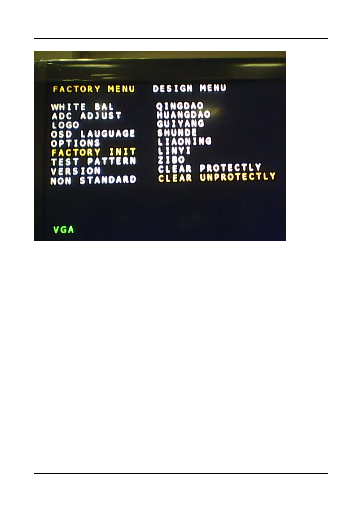
The Factory OSD Menu comprises Factory Menu and Design Menu .
2.2.1、Factory Menu
- 10 -
Page 11

FACTORY MENU
WHITE BALANCE
ADC ADJUST
LOGO
OSD LANGUAGE
COUNTRY
OPTIONS
FACTORY INIT
TEST PATTERN
VERSION
NON STANDARD
ADC ADJUST
Only in component and VGA
SOURCE ,The “
Can be chosen.
ADC Adjust”
WHITE BALANCE
COL TEMP STANDARD
R CUT 128
G CUT 128
B CUT 128
R DRV 128
G DRV 128
B DRV 128
LOGO
NULL
HISENSE
WELCOME
- 11 -
Page 12

OPTION
SOURCE TV
TOFAC M
ATS 1
STARTUP MENU 1
Search Sensitive 1
RF NTSC 0
HDCP OUT OR IN 1
TEST PATTERN
TEST PATTERN NULL
FACTORY INIT
QINGDAO
HUANGDAO
HUNGARY
FRANCE
AUSTRALIA
CLEAR PROTECTLY
CLEAR UNPROTECTLY
VERSION
VERSION:
PANEL TYPE:
FLASH :
2.2.2、Design Menu
- 12 -
Page 13

DESIGN MENU
PICTURE MODE
SOUND MODE
PICTURE CURVE
AUDIO CURVE
SSC SETTING
SAVING MODE
PICTURE MODE
MODE STANDARD
BRIGHTNESS 50
CONTRAST 50
COLOUR 50
PICTURE CURVE
MODE BRIGHTNESS
CURVE 0 97
CURVE 25 105
CURVE 50 120
CURVE 75 130
CURVE 100 141
SOUND MODE
MODE USER
120HZ 10
500HZ 10
1.5KHZ 10
5KHZ 10
10KHZ 10
AUDIO CURVE
MODE VOLUME
CURVE 0 0
CURVE 25 18
CURVE 50 22
CURVE 75 28
CURVE 100 36
- 13 -
Page 14

SSC SETTING
DDR SSC 2
DDR MCM 60
LVDS SSC 2
LVDS PCM 60
SAVING MODE
255
Note:
The above “Factory/Service OSD Menu” are reference only, please refer to the actual units
to determine the appearances.
- 14 -
Page 15

3. Software Upgrading
Before upgrading, read the following.
1、Before upgrading,Write down the ADC Calibration values of the channel of VGA and
component。
2、Upgrade the software.
3、To clear the EEPROM .
A Select the item “Clear Unprotected”.
B Press VOL+ button to clear the EEPROM data.
C Close the OSD menu after 5 seconds.
D Restart the TV.
4 Write the ADC Calibration values copied just now into the the channels of VGA and
component.
5、After the operation above all, necessarily, Renew search the channels for the users.
3.1 Get ready for upgrading
The software is upgraded by a burning tool- ISP_TOOL4.0.9, which can burn the
program file“*.bin” to the main board of the unit
3.1.1 Install the ISP_TOOL4.0.9-------only for the first time update.
1、 Port Setting:
- 15 -
Page 16
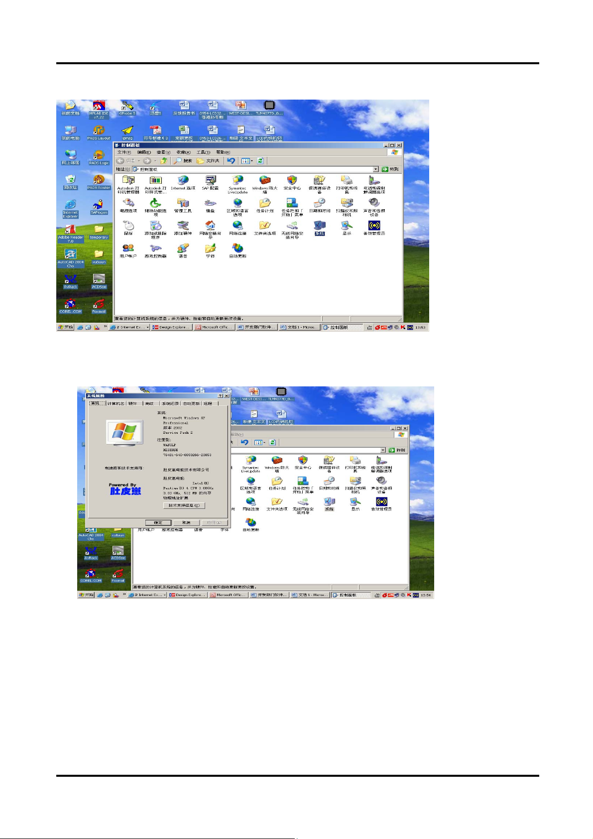
Choose “system”option from the “control panel”
Click the “system” icon as the following
Choose the “hardware” option from the dialog window
- 16 -
Page 17
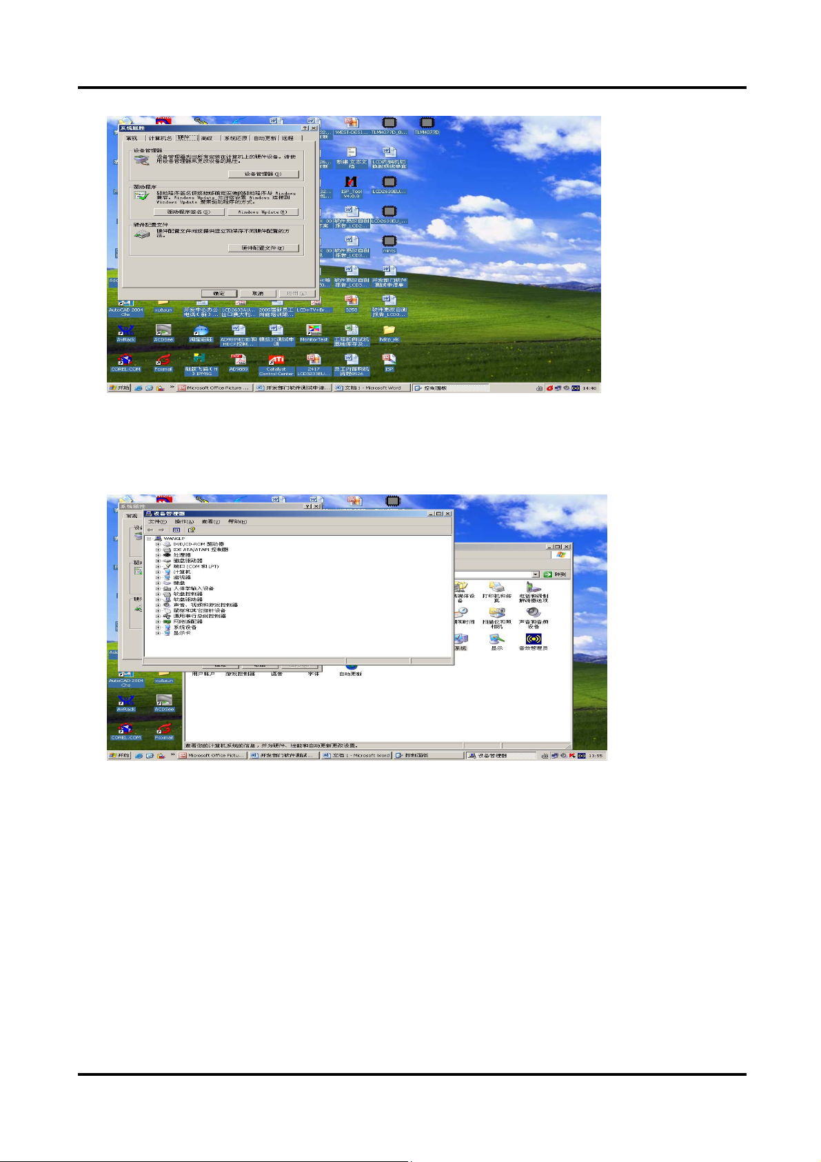
Click“device management” icon as the following
Choose the port (COM and LPT1)
- 17 -
Page 18
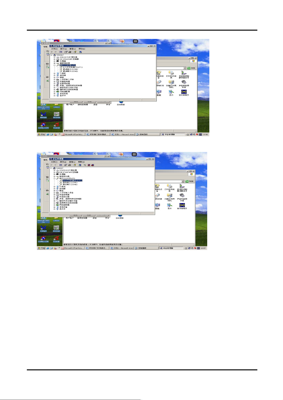
Choose the ECP print port (LPT1)
Click the port of print (LPT1)as the following
- 18 -
Page 19
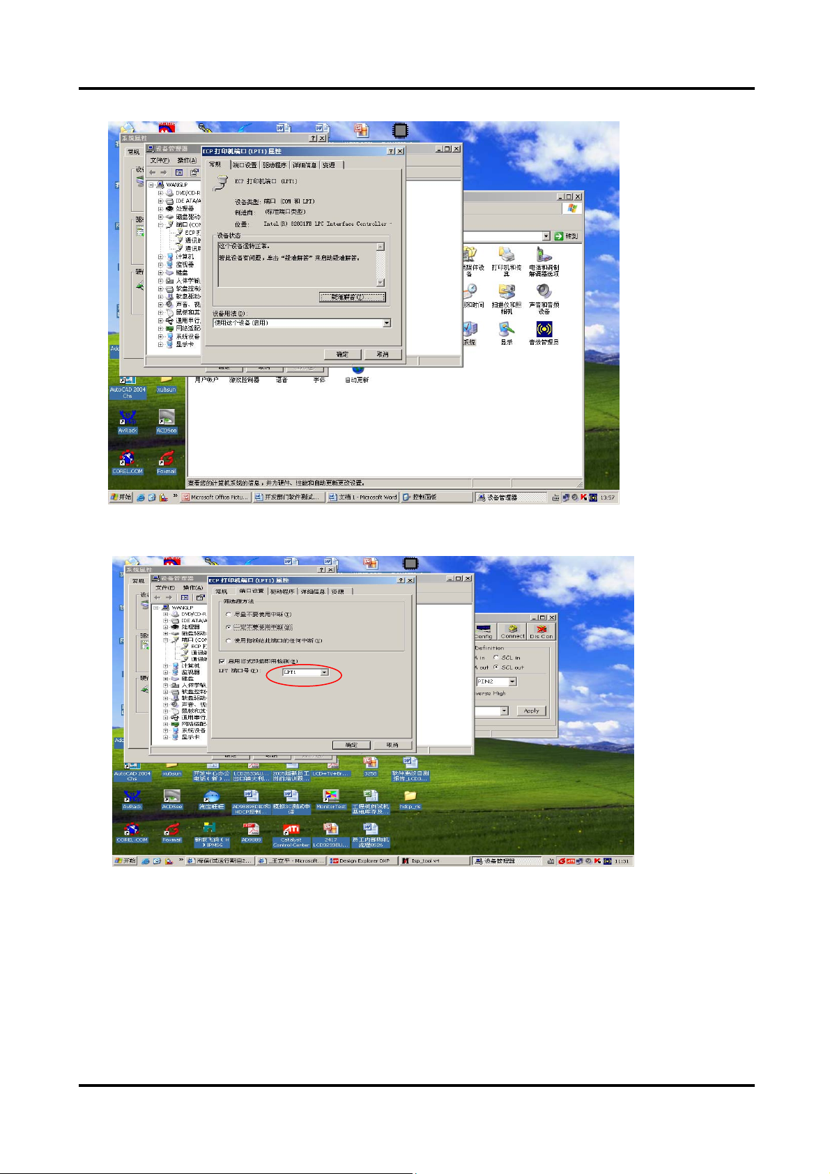
Choose “port setting”option as the following
- 19 -
Page 20
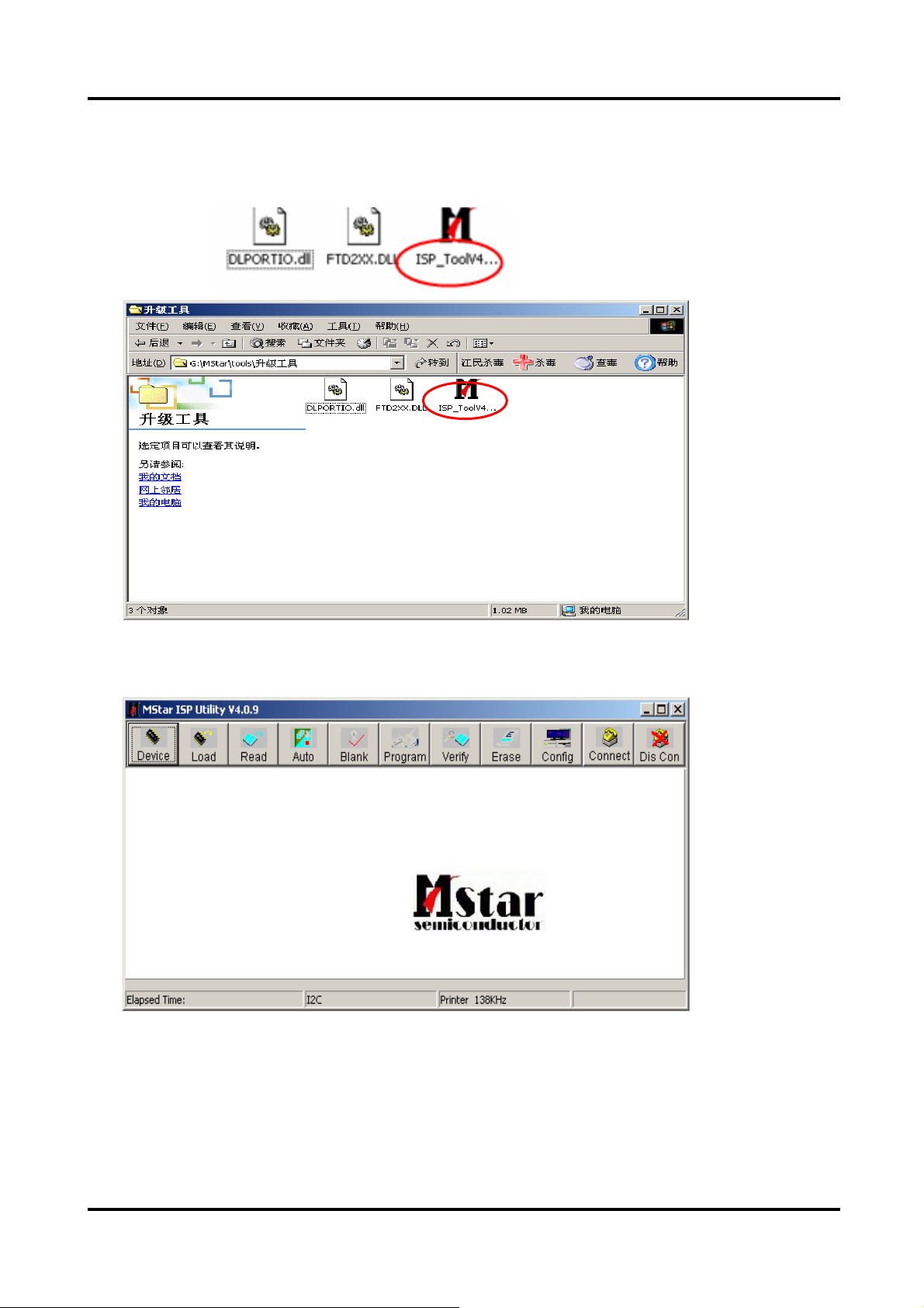
2、 Find the folder where the ISP_TOOL4.0.9 lies in.
There are three folders/files in this folder together.
DLPORTIO.dll and FTD2XX.DLL must be in the same folder
Double click the ISP_TOOL4.0.9 icon, and then a dialog window will show as below.
- 20 -
Page 21
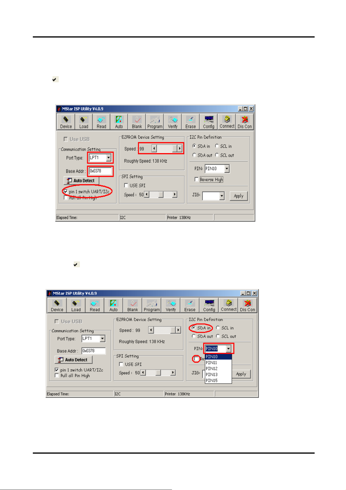
Click the Config button. And then a dialog window will show as below.
Port Type setting is LPT1
Base Addr setting is 0x378
Draw on the front of “pin 1 switch UART/I2c”
Speed setting is 99
As following
Choose“SDA in”and setting “PIN” is “PIN10”。
Notes:
Do not draw on the front of “Reverse High”。
As following
- 21 -
Page 22

Choose “SCL in”and setting “PIN” is “PIN11”。
Notes:
Do not draw on the front of “Reverse High”。
As following
Choose “SDA out”and setting “PIN” is “PIN4”
Notes:
Draw on the front of “Reverse High”。
As following。
Choose “SCL out”and setting “PIN” is “PIN2”
Notes:
Draw on the front of “Reverse High”
As following
- 22 -
Page 23

After having finished all above, clicking the “Apply ”button to complete the configuration。
3.1.2 Hardware connecting
You can update the software through a special tool (as following)
Connect the Debug board to the TV use VGA interface, the other parallel port to the
- 23 -
Page 24

computer, just as the following。
- 24 -
Page 25

3.2 Upgrading with the ISP_TOOL4.0.9
3.2.1 Double click the ISP_TOOL4.0.9 icon and a dialog window will show as following。
Click the“Read ”button。
- 25 -
Page 26

Choose the update file from the folder。
- 26 -
Page 27

The update file has been chosen successfully。
Click the“Auto”button and choose parameters as following。
Click the“Run”button
Click the“connect”button,then show a dialog box as following。
- 27 -
Page 28
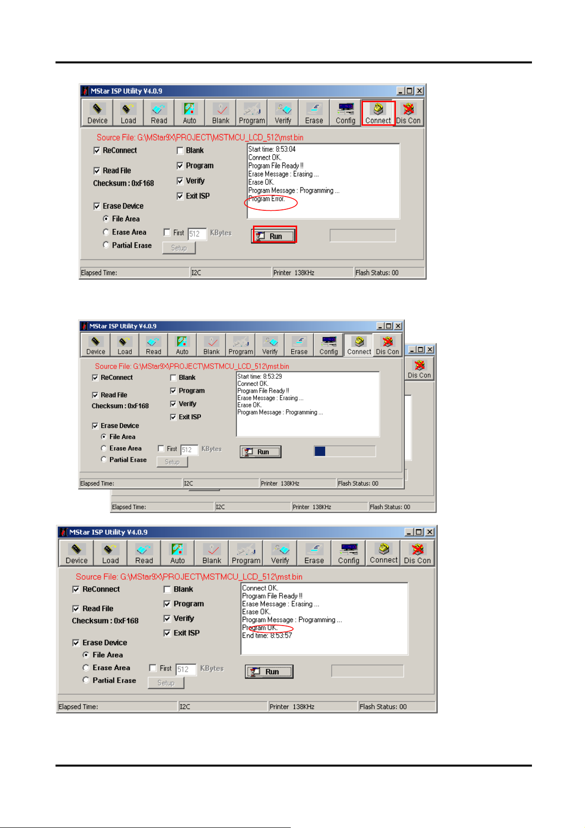
If show above then click the“Run”button again and again,till show the following dialog
window。
- 28 -
Page 29

The above appears on the screen-the word “program ok”shows in the information
displaying window,indicating upgrading is over。
3.2.2 After the update is over. Must Confirm the software Version in the Version Menu.
If the update is successful, enter Factory Init Menu and select “Clear Unprotectly”
a. Press VOL+ button to clear the EEPROM data.
b. When the “Clear Unprotectly ” button becomes white, turn off the power.
c. Restart the TV.
3.3 USB Software upgrading
3.3.1、Copy the Updating software to the USB root directory, the software named
*.bin. for example the TV LCD19W58AM(30) named LCD19W58AM.bin. If the TV
has internet function, Insert the USB disk to the interface nearly the Tuner.
- 29 -
Page 30
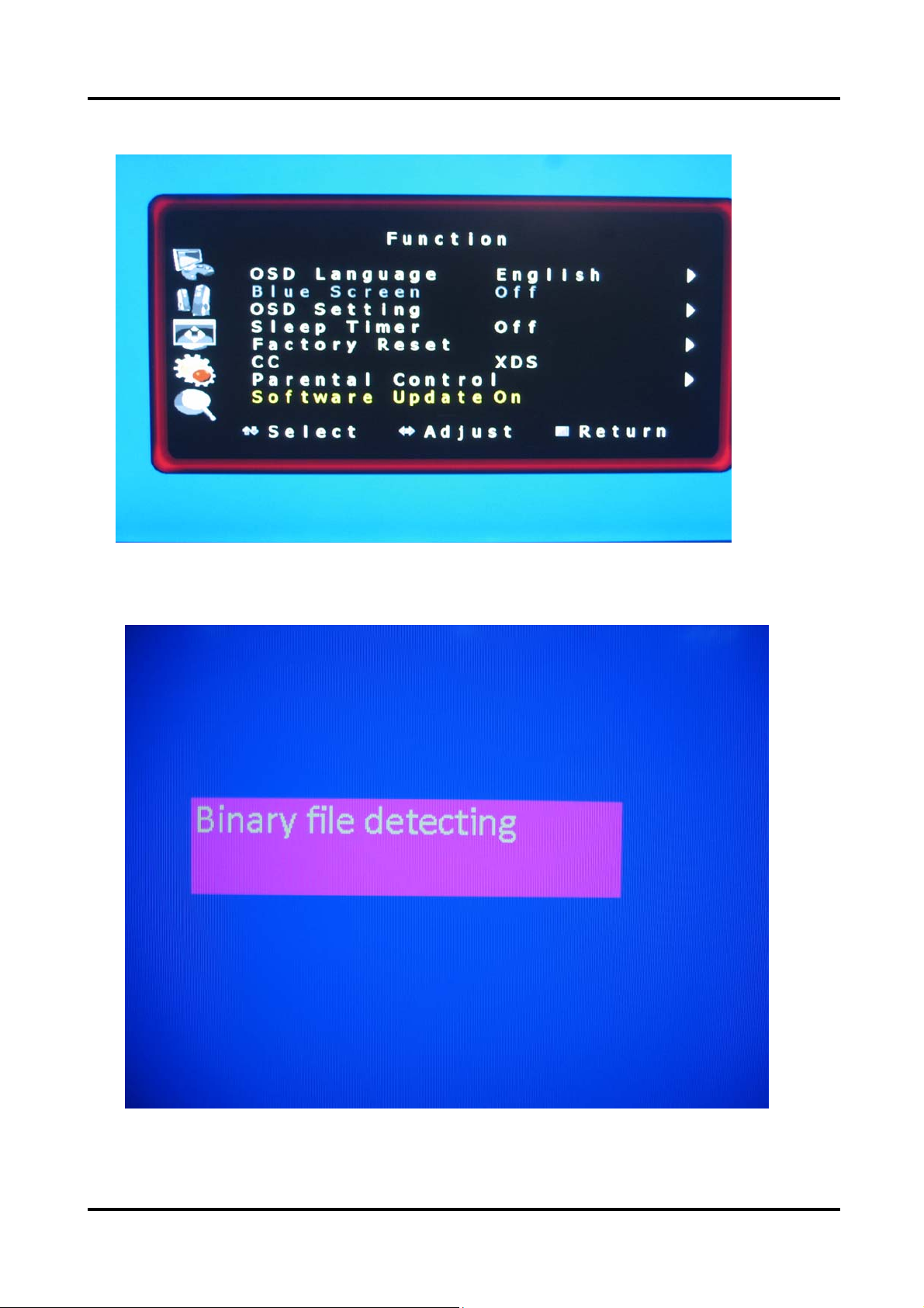
3.3.2the “Function” Menu “Sof tware Up date”choose“on”,see the next figure。
3.3.3 ACpoweroff,thenrestarttheTV.
- 30 -
Page 31

- 31 -
Page 32

3.3.4 After update success,ACpoweroff,andrestarttheTV.
Ifonlyappearthefigure:“Binaryfiledetecting”,thelastthreefiguresnot.Pleasemodifythe
nameofsotrware.
3.3.5、 After the update is over. Must Confirm the software Version in the Version
Menu.
If the update is successful, enter Factory Init Menu and select “Clear Unprotectly”
d. Press VOL + button to clear the EEPROM data.
e. When the “Clear Unprotectly ” button becomes white, turn off the power.
f. Restart the TV.
- 32 -
Page 33
3.3.6、Chasis MST6E16 includes 6E16GS and 6E16JS
Chassis 6E16GS must be the last 8 bit figures and letters in front ot .bin For example :
LCD19W58AM(30) named D19W58AM.bin.
Chassis 6E16JS must be the TV name in front of.bin. For example : LCD19W58AM(30)
named LCD19W58AM.bin.
- 33 -
Page 34

4. Circuit instruction
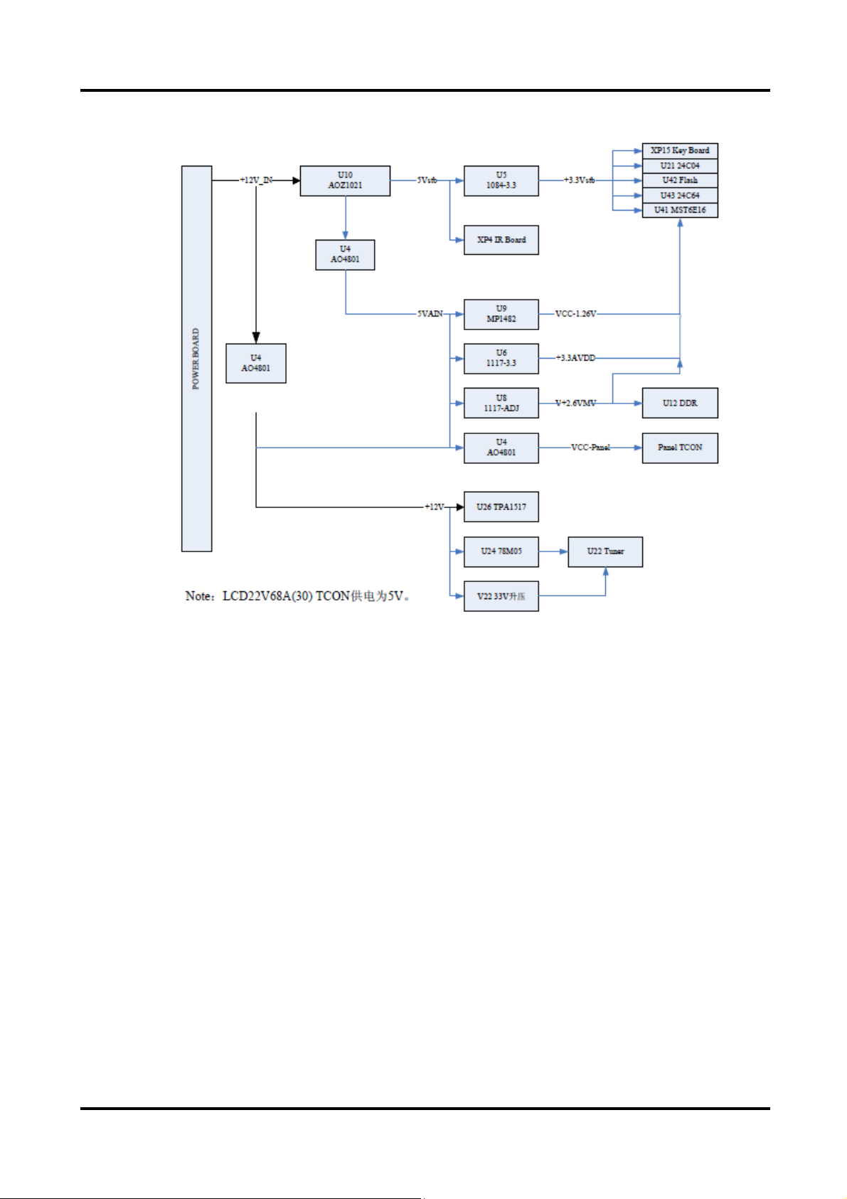
4.1 Main board Power assign and block diagram
Power assign:
The Powerd only has 12V output ,other voltages are converted from 12V.
a. 5Vstb is converted by U10 from 12V,5VAIN and +5V_USB are converted by U7 from 5Vstb.
b. +3.3Vstb that standby power supply for main IC (U41)、Flash (U42)、EEPROM (U43)、HDCP EEPROM
(U21)、Key is converted by 5Vstb from U5.
c. U28 and U30 power supply from 5VAIN
d. +3 .3AVDD su pply power for main is converted by U6 from 5VAIN; +2.6VM supply power for DDR is
converted by U8 from 5VAIN; VCC-1.26V supply power for main IC(core voltage) is converted by U9
from 5VAIN;
e +12V supply power for audio amplify is converted by U6 from +12V_IN; 5V-IN supply power for Tuner
is converted by U24from +12V_IN;
f VCC-Panel supply power for Panel is converted by U4 from 5VAIN or +12V_IN
Block diagram:
- 34 -
Page 35
4.2 Image and signal process
- 35 -
Page 36

TPA3101D2
e. RF Signal
RF Signal pass Tuner(U22) and surface acoustic wave filter(U23、U25) then output SIF and VIF signal,
which input to the main IC to have convert.
TPA3101D2
f. AV Signal
The video signal of AV input from terminal XS2,last enter the pin 37 of U41. as following
The CVBS video signal of SCART input from terminal XS39, last enter the pin35 of U41.
as following
- 36 -
Page 37

The YC video signal of S-Video input from terminal XS31, last enter pin 32、33 of U41. as
following
The RGB video signal of SCART input from terminal XS39, Ypbp r video signal of SCART input
from terminal XS7. The two signals pass U30 (IC\P15V330Q), then enter pin17-20 of U41. last pass
XP11/J2 directly output to the Panel
a
- 37 -
Page 38

b
PC(VGA)signal input from Terminal XS39, after having converted,. last enter the pin 22、24、
25、26 of U41.
Audio signal of HDMI and USB directly input IC U41.
Output of Scart (owning to have CANAL+ function , only output RF Signal)which by Pin 40 of
U41, As the following amplified circuit.. Output from terminal XS39.
g. Audio Signal (except HDMI and USB)
Audio Signal of TV is that the SIF signal pass through Tuner(U22) and surface acoustic wave
filter(U23、U25) was converted by U41.
- 38 -
Page 39

Audio XS7(YPbPr and VGA mutual the channel) Audio XS2 (AV and SV mutual the channel)
2. Control Process:
The Power only has 12V output ,other voltages are converted from 12V. U4 and U7 can interrupt other
voltages while standby, only reserve standby 5V. as following. When TV Power on , Standby Signal is High
level, 5VAIN Power suppluy normally ; When TV standby , the U7 tuner switch is shut off , 5VAIN Po wer
suppluy is low.
+12V standby signal control as similar as +5V
- 39 -
Page 40
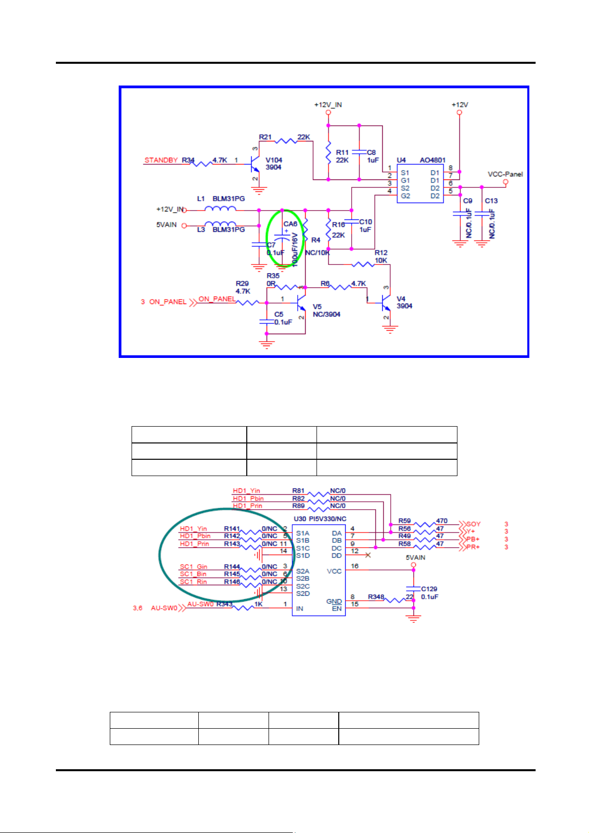
The video input signal of SCART RGB and Component was converted by U30, controlled by AU-SW0
signal. According current signal choose one channel output from 4、7、9 of U30
The control method as following:
Current channel AU-SW0 Switch output signal
Component Low level Component YPbPr
SCART High level SCART RGB
The audio input signal of SCART and AV was converted by U28, controlled by AU-SW0、AU-SW1
signal. According current signal choose one channel output from 3、13 of U U28
The control method as following:
Current channel AU-SW0 AU-SW1 Switch output signal
AV/SV Low level x AV/SV L/R
- 40 -
Page 41

SCART High level x SCART RGB
The main control signal, as list:
Control Signal
Standby signal(Power
control)
BL-control
L VDS VCC
Audio amplify mute AMP-MUTE High level mute
33V PWM
Key “0” Key0-in Key
Internet mark
STANDBY
PW_CTL High level power on
BL-ON/OFF
ON_PBACK Low level power on
ON_Panel High level TCON on
PWM3
recommend Remark
High level power on
High level power on
33V rising voltage circuit
PW_CTL pass V1、V26
inverse phase
ON_PBACK pass V2
inverse phase
- 41 -
Page 42

Key “1” Key1-in Key
Remote control signal IR-SYNC IR
4.3 The main IC description
74HC4052D:
- 42 -
Page 43

- 43 -
Page 44

AOZ1021
- 44 -
Page 45

RF7314
- 45 -
Page 46
- 46 -
Page 47
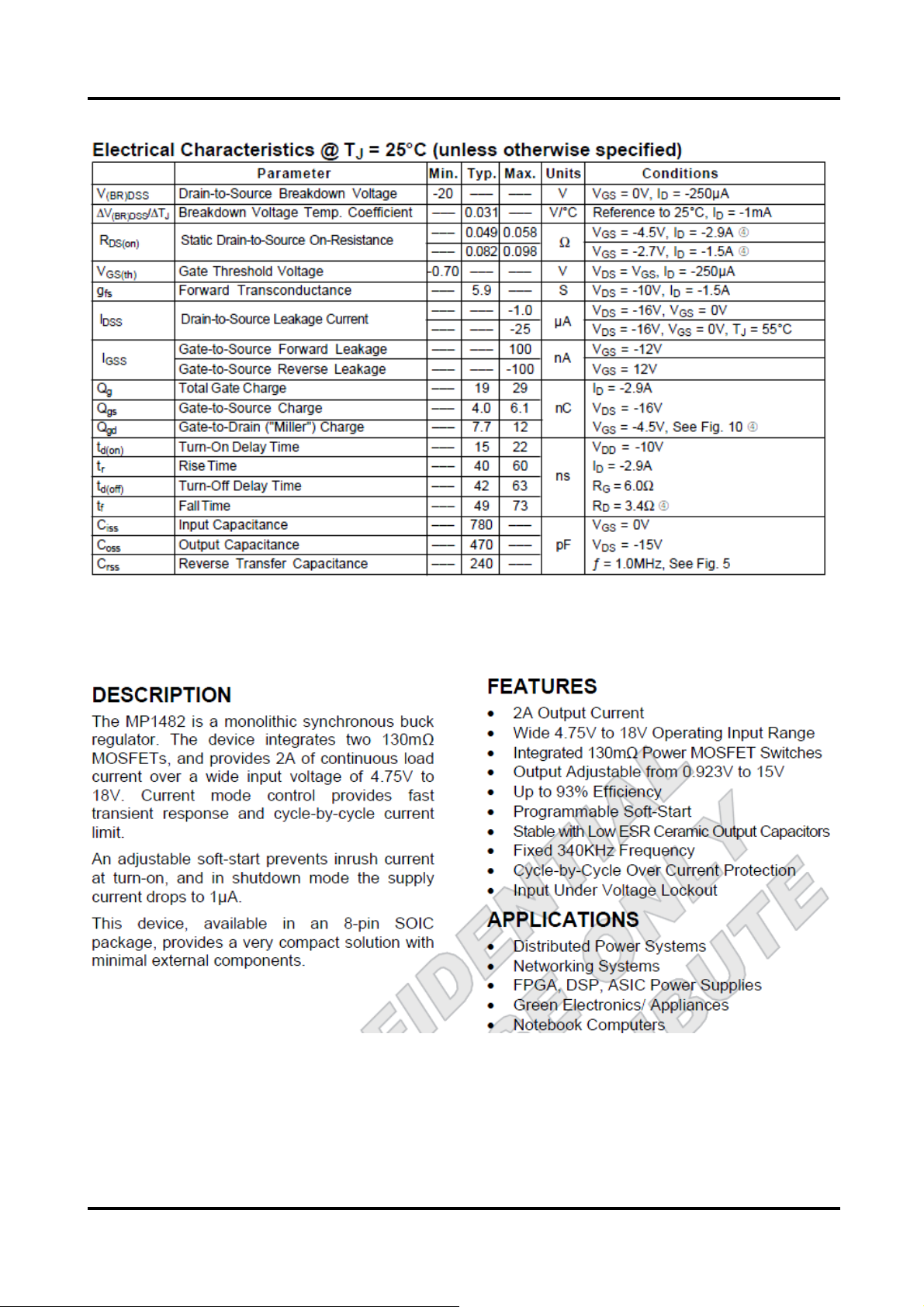
MP1482
- 47 -
Page 48

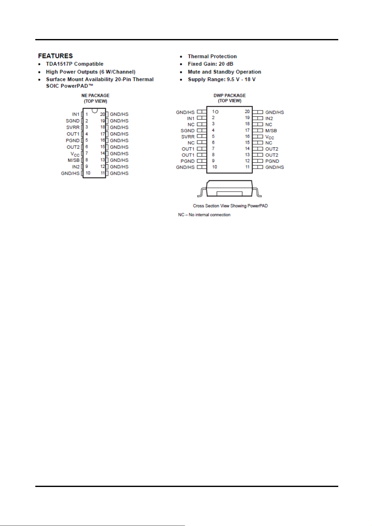
TPA1517
- 48 -
Page 49
- 49 -
Page 50

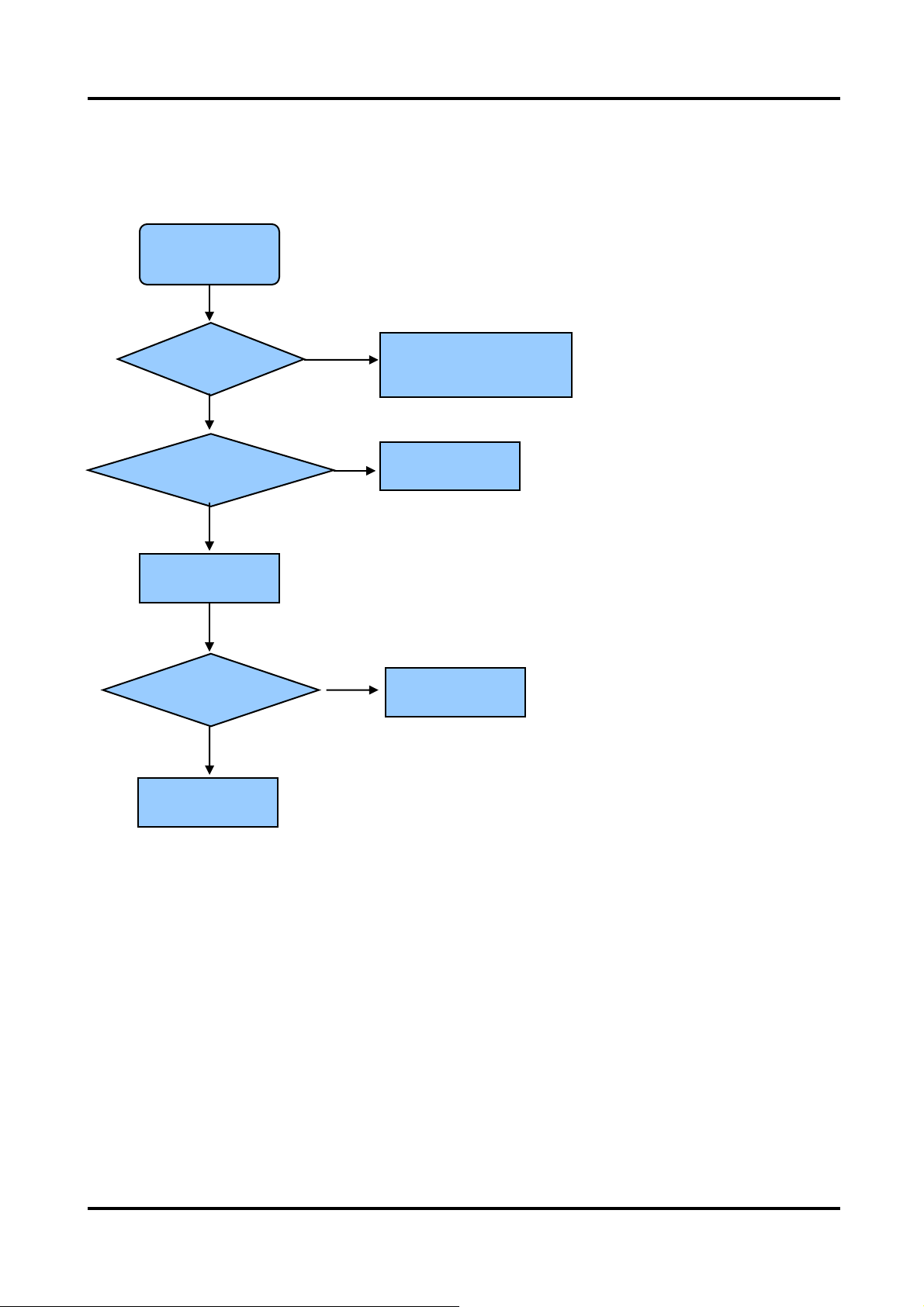
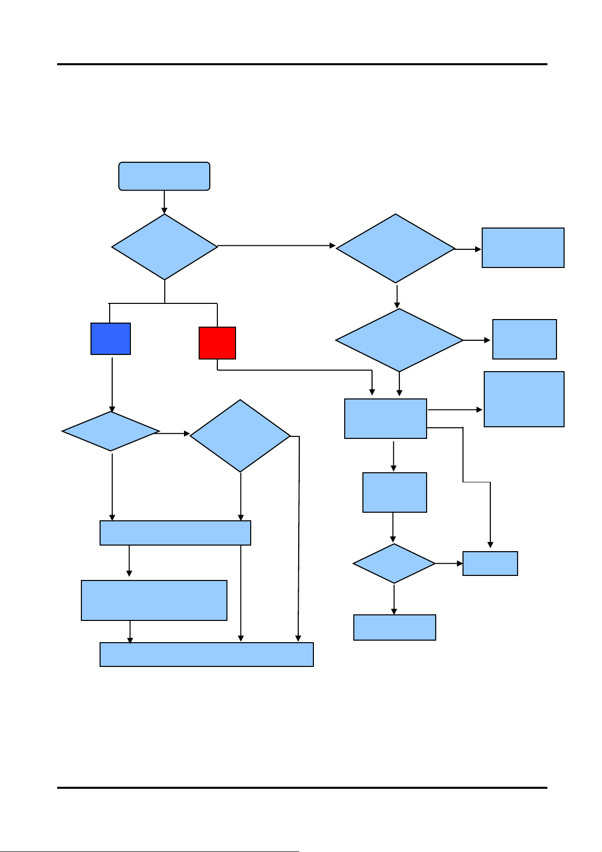
4.4 Troubleshooting
4.4.1 Troubleshooting for Remote Control
Remote control does not work
Try new batteries
NO
Replace RC
Check IR receiver
YES
YES
Replace battery
Replace remote control
Change Led & IR board
NO
Change Led & IR cable
NO
Replace main board
YES
Replace Led & IR BD
YES
Replace Led & IR cable
- 50 -
Page 51
4.4.2 Troubleshooting for Function Key
Buttons does not work
Check switches
YES
Check solder connections and
see if any switches are stuck.
NO
Check key board
NO
Check Key BD cable
YES
Replace Key BD
YES
Change Key BD
OK
NO
Replace main board
- 51 -
Page 52
4.4.3 TV won’t Power On
TV won’t power on
Is LED
light?
NO
Check Power
Output
YES
Make Sure Power
source is live
YES
NO
BLUE
RED
Panel Bright
NO
YES
Check signal
Source
YES
NO
Check Power
Cord
NO
Try Power on by
RC and Button
Neither
works
Replace Main
BD
YES
Only
one works
Both
Work
Replace
Power Cord
Check/replace IR
BD or Keypad
PCA
NO
(to contact Hisense tech support.)
Replace Main BD
Replace Panel
OK
YES
Power on
NO
Replace Power BD
YES
OK
- 52 -
Page 53

4.4.4 Troubleshooting for Audio
No sound
Check connecter
YES
Reconnect
NO
Check speaker wire
NO
Check speaker set
YES
YES
Replace speaker wire
Replace speaker set
NO
Replace main board
NO
YES
OK
Power Supply Board
- 53 -
Page 54

4.4.5 Troubleshooting for TV/VGA/HDMI input
No picture on the screen
NO
Check Signal Source
Make sure signal
source is available
YES
Check connect
NO
YES
Check cab l e
NO
Replace main board
Reconnect
Replace cable
- 54 -
Page 55

4.4.6 Troubleshooting for YPbPr input
No picture on the screen
Check Source work or not
YES
Check connect
NO
Check Wires (Green Blue, Red)
NO
Replace main board
NO
YES
YES
Check Source Device
Reconnect
Replace wires
- 55 -
Page 56

4.4.7 Troubleshooting for Video/S-Video input
No picture on the screen
Check Source work or not
YES
Check connect
NO
Check Cable/ Wires
NO
Replace main board
NO
YES
YES
Check Signal Source
Reconnect
Replace Cable/Wires
- 56 -
Page 57

5. Schematic circuit diagram
- 57 -
Page 58

474/AC250V
C801
1
2
3
TJC2-3A
XP801
1WB60
VB901
474/AC275V
C803
102/AC250V
C805
102/AC250V
C804
270k
R801
10D561
RV801
t
NTC5D-20
RT801
T6.3A/250VAC
F801
100K/2W
R901
4u7/450V
C903
22uF/50V
C906
470u/16V
C907
1N5819
VD903
104
C904
470P/1KV
C905
75R
R903
100u/16V
C908
L901
100R
R904
680R
R905
2K4
R906
2K4
R909
100K
R908
1K
R907
104
C909
104
C910
RG1C
VD901
1N5819
VD902
MBRF20H100
VD838
24V
3V3
VZ833
103/630V
C842
24V/8A
1000u/35V
C843
PC817B
N833
1K
R863
12V/2A
12V
5V_M
STB
SW
474/16V
C831
8k2
R834
1
2
3
4
XP-04
Q801
1
2
3
4
XP-04
Q802
56P/1KV
C841
474
C839
1N4148
VD832
5k1
R847
10k
R846
120R
R843
15K
R837
104/50V
C837
105
C833
105
C832
15k
R838
5k1
R835
2M2
R836
22uF/25V
C838
102/50V
C834
1k
R854
2K
R844
1K
R848
10K
R845
3K3
R840
5K6
R839
22R
R842
104/50V
C836
MUR160
VD831
2907
V803
3V3
VZ832
104/50V
C840
75K
R850
2K4
R853
2K
R852
75K
R851
1N4148
VD836
5K1
R858
68R
R857
68R
R856
2K
R841
VCC
BZT52C18
VZ831
102/50V
C835
LCL-2420H
L801
LCL-2420H
L802
102/2KV
C806
471/AC275V
C808
120R
R828
PFC
5VS
G1
G2
G3
102/2KV
C807
PFC
1/2/7/8S
4FB
3BP
5D
LINK564
N901
PC817B
N902
4 10
76
2
1
T901 5VS
5VS/1A
300v
5VS
1N4148
VD905
AC1
AC2
300V
OMI-SS-212DM
J801
220u/450V
C810
100K/2W
R815
SFF806
VD812
224/50V
C819
330R
R822
104/50V
C816
560K
R823
18V
VZ812
NC
C815
20K
R816
NC
C818
224/50V
C820
200K
R827
20N60
V810
0.22/3W
R820
MUR460
VD811
10K
R826
68R
R819
512
R817
18V
VZ811
68R
R818
0520
VD815
101/50V
C817
NC
R829
20K
R814
1M
R813
1M
R812
1M
R811
300v PFC
EU2A
VD813
EU2A
VD814
VCC
PFC
NC
R830
NCP33262
1
2
3
4
5
7
6
8
Zcd
Multi
Comp
Vcc Dri
CS
VFB
GND
N811
3
8
10
6
7
9
L811
L811
1N4148
VD816
102/50V
C821
5VS
5V-M/4A
5V_M
102
C912
5u/7A
L902
104
C911
1000u/16V
C917
1000u/16V
C918
1N4148
VD907
24V
12V
MUR460
VD841
1000u/25V
C848
1K/3W
R870
18V
18V
5A
F831
1N5822
VD904
SW
10N60
V831
5K1
R861
68R
R860
68R
R859
1N4148
VD834
1N4148
VD835
VCC
CSS
1
Fmax
2
Ctimer
3
RT
4
BO
5
FB
6
DT
7
FF
8
SF
9
GND
10
Mlower
11
Vcc
12
13
HB
14
Mupper
15
Vboot
16
NCP1396
N831
104/50V
C847
1K0
R864
18K
R865
7K5
R866
200K
R8681KR869
1K
R867
474
C849
13
10
11
16
8
14
12
9
3 15
1
T831
RM11C
VD842
18V/2A
KA431AZ
N903
TL431
N832
TL431
N834
10k
R911
68R
R915
10R
R918
10R
R919
30K
R920
1K
R921
NC
R922
5K6
R923
27
R889
104
C914
104
C913
102
C822
1
2
3
4
5
6
7 8
Vcc
TG
Comp Ph
FB
GND
BG
Bst
NCP1579
N904
1
2
34
5
6
7
8
D2
G1D1D1
D2
S1
G2 S2
NTMD4820N
V905
W808
1
2
3
4
5
6
7
8
9
10
11
12
13
14
XP-14
XP802
1
2
3
5
7
4
6
8
XP-08
XP806
PWM
1
2
3
4
5
6
7
8
9
10
11
12
XP-12
XP803 24V
1
2
3
4
5
6
7
8
9
10
11
12
13
14
XP-14
XP804
PWM
12V
1
2
3
4
5
6
7
8
9
10
11
12
13
XP-13
XP805
5V_M
12V
270k
R802
270k
R803
22u/50V
C814
0.22/3W
R821
560K
R824
560K
R825
1M
R831
1M
R832
1M
R833
MBRF20H100
VD839
MBRF20H100
VD840
10N60
V832
1N4148
VD837
1000u/35V
C844
1000u/35V
C845
2200u/25V
C846
2K2
R862
1000P/400V
C901
2200P/400V
C850
1000P/400V
C851
10A/600V
VB801
12V
10K
R917
1K
R916
2222A
V901
104
C916
STB
100K/2W
R810
RM11C
VD843
22u/50v
C813
47u/25v
C811
47u/25v
C812
(EMC)
(EMC)
(EMC)
(EMC)
(EMC)
P0F80102 P0F80104
P0F80102 P0F80104
P0XP80101 P0XP80102 P0XP80103
P0XP80101
P0XP80101
P0XP80102 P0XP80103
P0XP80102 P0XP80103
P0F80101 P0F80102 P0F80103 P0F80104
P0F80101 P0F80103
P0F80101 P0F80103
P0C80102
P0C80102
P0C80101 P0C80102
P0C80101
P0C80101
P0R91602
P0R91602
P0RV80101 P0RV80102
P0RV80101
P0RV80101
P0RV80102
P0RV80102
P0R91601 P0R91602
P0R91601
P0R91601
P0RT80102
P0RT80102
P0L80101 P0L80102
P0L80101
P0L80101
P0L80104
P0L80104
P0L80102
P0L80102
P0L80103 P0L80104 P0L80201 P0L80202
P0L80103
P0L80103
P0V90101
P0V90101
P0V90101
P0C91602
P0C91602
P0C91601 P0C91602
P0C91601
P0C91601
P0R91701 P0R91702
P0R91701
P0R91701
P0R91702
P0R91702
P0VD90501 P0VD90502
P0VD90501
P0VD90501
P0V90103
P0V90103
P0V90102 P0V90103
P0V90102
P0V90102
P0RT80101 P0RT80102
P0RT80101
P0RT80101
P0J80104
P0J80104
P0J80104
P0J80101
P0J80101
P0J80101
P0VD90502
P0VD90502
P0R80102
P0R80102
P0R80101 P0R80102 P0R80201 P0R80202 P0R80301 P0R80302
P0R80101 P0R80202 P0R80201 P0R80302
P0R80101 P0R80202 P0R80201 P0R80302
P0C80301 P0C80302
P0C80301
P0C80301
P0C80302
P0C80302
P0R80301
P0R80301
P0J80103
P0J80103
P0J80102 P0J80103
P0J80102
P0J80102
N05VS
P0C80501
P0C80501
P0C80401 P0C80402 P0C80501 P0C80502
P0C80401 P0C80502
P0C80401 P0C80502
P0C80402
P0C80402
P0VD81101 P0VD81102
P0VD81101
P0VD81102
P0VD81101
P0VD81102
P0L80204
P0L80204
P0L80201
P0L80201
P0VB80101
P0VB80101
P0L80203 P0L80204
P0L80203
P0L80203
P0VB80102 P0VB80103
P0VB80102
P0VB80102
P0L80202
P0L80202
P0VB80101
P0VB80104
P0VB80104
P0VB80104
P0VB80103
P0VB80103
N0300V
N0300V
P0C80701
P0C80701
P0C80601 P0C80602 P0C80701 P0C80702
P0C80601 P0C80702
P0C80601 P0C80702
P0C80602
P0C80602
P0300V
P0300V
P0300V
P0C80802
P0C80802
P0C80801 P0C80802
P0C80801
P0C80801
P0C90101 P0C90102
P0C90102
P0C90101
P0C90102
P0C90101
P0C85001 P0C85002
P0C85002
P0C85001
P0C85002
P0C85001
P0C85101 P0C85102
P0C85102
P0C85101
P0C85102
P0C85101
P0VB90103 P0VB90104
P0VB90103
P0VB90103
P0VB90101 P0VB90102
P0VB90101
P0VB90101
P0VB90104
P0VB90104
P0VB90102
P0VB90102
P0C90301 P0C90302
P0C90301
P0C90301
P0C90302
P0C90302
P0N90104
P0N90104
P0N90104
P0N90101
P0N90107
P0N90101
P0N90107
P0N90101
P0N90107
P0N90105
P0N90105
P0N90105
P0N90103
P0N90103
P0N90103
P0N90102
P0N90108
P0N90102
P0N90108
P0N90102
P0N90108
P0C90502
P0C90502
P0C90501
P0C90501
P0VD90102
P0VD90102
P0VD90101 P0VD90102
P0VD90101
P0VD90101
P0R90301 P0R90302
P0R90301
P0R90301
P0C90402
P0C90402
P0C90401 P0C90402 P0C90501 P0C90502
P0C90401
P0C90401
P0R90101 P0R90102
P0R90101
P0R90101
P0R90102
P0R90102
P0R90302 P0VD90202
P0R90302 P0VD90202
P0C90601 P0C90602
P0C90601
P0C90601
P0C90602
P0C90602
P0VD90201 P0VD90202
P0VD90201
P0VD90201
P0N90204
P0N90204
P0N90204
P0N90203
P0N90203
P0T90106
P0T90106
P0T90106
P0T90107
P0T90107
P0T90107
P0VD90301 P0VD90302
P0VD90301
P0VD90301
P0VD90302
P0VD90302
P0T901010
P0T901010
P0T90104
P0T90104
P0T90104
P0T90102
P0T90102
P0T90102
P0T90101
P0T90101
P0T90101
P0T901010
P0N90201
P0N90201
P0N90201
P0C90701 P0C90702
P0C90701
P0C90701
P0C90702
P0C90702
P0R90401 P0R90402 P0R90501 P0R90502
P0R90401
P0R90401
P0R90402 P0R90501
P0R90402 P0R90501
P0L90101 P0L90102
P0L90101
P0L90101
P0C90901 P0C90902
P0C90901
P0C90902
P0C90901
P0C90902
P0L90102
P0L90102
P0R90601 P0R90602
P0R90601
P0R90601
P0R90602
P0R90602
P0N90202 P0N90203
P0N90202
P0N90202
P0R90502
P0R90502
P0C81301 P0C81302
P0C81301
P0C81301
P0C81302
P0C81302
P0N90303
P0N90303
P0N90301
P0N90301
P0N90301
P0N90302 P0N90303
P0N90302
P0N90302
P0C91001 P0C91002
P0C91001 P0R90702
P0C91001 P0R90702
P0R90801 P0R90802
P0R90801
P0R90801
P0R90701 P0R90702
P0R90701
P0R90701
P0R90802
P0R90802
P0C91002
P0C91002
P0R90901 P0R90902
P0R90901
P0R90901
P0R90902
P0R90902
N05VS
N05VS P0C90801
P0C90801 P0C90802
P0C90801
P0C90802
P0C90802
P05VS/1A
P05VS/1A
P05VS/1A
P0C81901 P0C81902
P0C81901
P0C81901
P0C81902
P0C81902
P0C82001 P0C82002
P0C82001
P0C82001
P0C82002 P0R82701
P0C82002 P0R82701
P0R82701 P0R82702
P0R82702
P0R82702
N0300V
P0R81101 P0R81102 P0R81201 P0R81202 P0R81301 P0R81302 P0R81401 P0R81402
P0R81101
P0R81101
P0R81102 P0R81202 P0R81201 P0R81302
P0R81102 P0R81202 P0R81201 P0R81302
P0R81301 P0R81402
P0R81301 P0R81402
P0R81401
P0R81401
P0R81002
P0R81002
P0R81001 P0R81002
P0R81001
P0R81001
P0C82101 P0C82102
P0C82101
P0C82101
P0C82102
P0C82102
P0R81502
P0R81502
P0R81501 P0R81502
P0R81501
P0R81501
P0R82801 P0R82802
P0R82801
P0R82802
P0R82801
P0R82802
P0C81401 P0C81402
P0C81401
P0C81401
P0C81402
P0C81402
P0VD81601 P0VD81602
P0VD81601
P0VD81601
P0VD81602
P0VD81602
P0VZ81202
P0VZ81202
P0VZ81201 P0VZ81202
P0VZ81201
P0VZ81201
P0C81101 P0C81102 P0C81201 P0C81202
P0C81101
P0C81101
P0VD81302
P0VD81302
P0C81102 P0C81201
P0C81102 P0C81201
P0C81202
P0C81202
P0C81601 P0C81602
P0C81601
P0C81601
P0C81602
P0C81602
P0L81103 P0L81106
P0L81103
P0L81103
P0VD81301 P0VD81302
P0VD81301
P0VD81301
P0L81107
P0L81107
P0L81107
P0N81108
P0N81108
P0N81108
P0N81102
P0N81102
P0N81102
P0N81103
P0N81103
P0N81103
P0L81109
P0L81109
P0L81109
P0VD81402
P0VD81402
P0VD81401 P0VD81402
P0VD81401
P0VD81401
P0N81105
P0N81105
P0N81105
P0R82902
P0R82902
P0C81501 P0C81502
P0C81501
P0C81501
P0R82901 P0R82902
P0C81502
P0R82901
P0C81502
P0R82901
P0L81106
P0L81106
P0L811010
P0L811010
P0L811010
P0R81602
P0R81602
P0R81601 P0R81602
P0R81601
P0R81601
P0N81106
P0N81106
P0N81106
P0L81108
P0L81108
P0L81108
P0VD81502
P0VD81502
P0N81107
P0N81107
P0N81107
P0N81104
P0N81104
P0N81104
P0N81101
P0N81101
P0N81101
P0VD81501 P0VD81502
P0C81701 P0C81702
P0C81701
P0C81701
P0C81702
P0C81702
P0R81901 P0R81902
P0R81902 P0V81001
P0R81901 P0VD81501
P0R81902 P0V81001
P0R81901 P0VD81501
P0R81801 P0R81802
P0R81802
P0R81801
P0R81802
P0R81801
P0R82201 P0R82202
P0R82201
P0R82202
P0R82201
P0R82202
P0C81802
P0C81802
P0C81801 P0C81802
P0C81801
P0C81801
P0VZ81102
P0VZ81102
P0VZ81101 P0VZ81102
P0VZ81101
P0VZ81101
P0V81001
P0R81701 P0R81702
P0R81701
P0R81701
P0R81702
P0R81702
P0R82001 P0R82002
P0R82001
P0R82001
P0R82002
P0R82002
P0VD81201 P0VD81202
P0VD81201
P0VD81201
P0V81002 P0V81003
P0V81002
P0V81002
P0V81003
P0V81003
P0R82101 P0R82102
P0R82101
P0R82101
P0R82102
P0R82102
P0VD81202
P0VD81202 P0PFC
P0R82302
P0R82302
N0PFC
P0C81001 P0C81002
P0C81001
P0C81001
P0C81002
P0C81002
P0PFC
P0PFC
P0R82301 P0R82302 P0R82401 P0R82402 P0R82501 P0R82502 P0R82601 P0R82602
P0R82301 P0R82402 P0R82401 P0R82502
P0R82301 P0R82402 P0R82401 P0R82502
P0R82501 P0R82602
P0R82501 P0R82602
P0R83002
P0R83002
P0R82601
P0R82601
P0R83001 P0R83002
P0R83001
P0R83001
P0R92202
P0R92202
P0R92201 P0R92202
P0R92201
P0R92201
N012V
P0R91502
P0R91502
P0R92302
P0R92302
P0R92301 P0R92302
P0R92301
P0R92301
P0R92102
P0R92102
P0R92101 P0R92102
P0R92101
P0R92101
P0R91501 P0R91502
P0R91501
P0R91501
P0C91401 P0C91402
P0C91401
P0C91401
P0C91402
P0C91402
P0R91102
P0R91102
P0R91101 P0R91102
P0C91101 P0C91102
P0C91101 P0R91101
P0C91101 P0R91101
P0C91102
P0C91102
P0N90405
P0N90405
P0N90405
P0N90406
P0N90406
P0N90406
P0N90407
P0N90407
P0N90407
P0C91201 P0C91202
P0C91201
P0C91201
P0C91202
P0C91202
P0N90403
P0N90403
P0N90403
P0N90401 P0N90402
P0N90401
P0N90401
P0N90402
P0N90402
P0N90408
P0N90408
P0N90408
P0N90404
P0N90404
P0N90404
P0VD90701 P0VD90702
P0VD90701
P0VD90701
P0VD90702
P0VD90702
P0C91302
P0C91302
P0C91301 P0C91302
P0C82201 P0C82202
P0C82201 P0R88902 P0C82202 P0C91301
P0C82201 P0R88902 P0C82202 P0C91301
P0R88901 P0R88902
P0R88901
P0R88901
P0R91801 P0R91802
P0R91801
P0R91801
P0R91901 P0R91902
P0R91901
P0R91901
P0R92002
P0R92002
P0R92001 P0R92002
P0R92001
P0R92001
P0L90201 P0L90202
P0L90201
P0L90201
P0V90502
P0V90502
P0V90502
P0R91802
P0R91802
P0R91902
P0R91902
P0V90501
P0V90501
P0V90501
P0V90505
P0V90505
P0V90505
P0V90506
P0V90506
P0V90506
P0V90504
P0V90504
P0V90504
P0VD90401 P0VD90402
P0VD90401
P0VD90401
P0L90202
P0L90202
N012V
P0V90507 P0V90508
P0V90507 P0V90508
P0V90507 P0V90508
P0V90503
P0V90503
P0V90503
P0VD90402
P0VD90402
N05V0M
P0C91701 P0C91702
P0C91701
P0C91701
P0C91702
P0C91702
N05VS
P0C91801 P0C91802
P0C91801
P0C91801
P0C91802
P0C91802
P05V0M/4A
P05V0M/4A
P05V0M/4A
N0PFC
P0R83101 P0R83102 P0R83201 P0R83202 P0R83301 P0R83302 P0R83401 P0R83402
P0R83101
P0R83101
P0R83102 P0R83201 P0R83202 P0R83301
P0R83102 P0R83201 P0R83202 P0R83301
P0R83302 P0R83402
P0R83302 P0R83402
P0R83401
P0R83401
P0R83801 P0R83802
P0R83801
P0R83801
P0R83802
P0R83802
P0C83202
P0C83202
P0R83502
P0R83502
P0R83501 P0R83502
P0R83501
P0R83501
P0C83102
P0C83102
P0C83101 P0C83102 P0C83201 P0C83202
P0C83101 P0C83201
P0C83101 P0C83201
P0R83902
P0R83902
P0R83901 P0R83902
P0R83901
P0R83901
P0R83602
P0R83602
P0R83601 P0R83602
P0R83601
P0R83601
P0C83401 P0C83402
P0C83401
P0C83401
P0C83402
P0C83402
P0C83302
P0C83302
P0R83702
P0R83702
P0C83301 P0C83302
P0C83301
P0C83301
P0R84102
P0R84102
P0R84101 P0R84102
P0R84101
P0R84101
P0N83104
P0N83104
P0R83701 P0R83702
P0R83701
P0R83701
P0N83104
P0N83105
P0N83105
P0N83105
P0N83106
P0N83106
P0N83106
P0N83107
P0N83107
P0N83107
P0N83108
P0N83108
P0N83108
P0R84002 P0C83502
P0R84002 P0C83502
P0R84001 P0R84002
P0R84001
P0R84001
P0C83501 P0C83502
P0C83501
P0C83501
P0N83101
P0N83101
P0N83101
P0N83102
P0N83102
P0N83102
P0N83103
P0N83103
P0N83103
P0N831015
P0N831015
P0N831015
P0N831011
P0N831011
P0N831011
P0N831016
P0N831016
P0N831016
P0N831014
P0N831014
P0N831014
P0N831013
P0N831013
P0N831013
P0N831012
P0N831012
P0N831012
P0N831010
P0N831010
P0N831010
P0N83109
P0N83109
P0N83109
P0R84202
P0R84202
P0C83601 P0C83602
P0C83601
P0C83601
P0C83602
P0C83602
P0C83701 P0C83702
P0C83701
P0C83701
P0C83702
P0C83702
P0R84701 P0R84702
P0R84701
P0R84701
P0R84601 P0R84602
P0R84601
P0R84601
P0R84702
P0R84702
P0R84201 P0R84202
P0R84201 P0VD83102
P0R84201 P0VD83102
P0C83801 P0C83802
P0C83801
P0C83801
P0C83802
P0C83802
P0R84602
P0R84602
P0R84301 P0R84302
P0R84302
P0R84301
P0R84302
P0R84301
P0VZ83102
P0VZ83102
P0VZ83101 P0VZ83102
P0VZ83101
P0VZ83101
P0VD83201 P0VD83202
P0VD83201
P0VD83201
P0VD83202
P0VD83202
P0VD83101 P0VD83102
P0VD83101
P0VD83101
P0R84401 P0R84402
P0R84401
P0R84401
P0R84402 P0V80302
P0R84402 P0V80302
P0V80302 P0V80303
P0V80303
P0V80303
P0V80301
P0R84502 P0V80301
P0R84502 P0V80301
P0R84801 P0R84802
P0R84801
P0R84801
P0R84802 P0VZ83202
P0R84802 P0VZ83202
P0R84501 P0R84502
P0R84501
P0R84501
P0VZ83201 P0VZ83202
P0N83203 P0VZ83201
P0N83203 P0VZ83201
P0N83201
P0N83201
P0N83201
P0N83202 P0N83203
P0N83202
P0N83202
P0C83902
P0C83902
P0C83901 P0C83902
P0C83901
P0C83901
P0R85101 P0R85102
P0R85101
P0R85101
P0R85102 P0VD83402
P0R85102 P0VD83402
P0VD83401 P0VD83402
P0VD83401
P0VD83401
P0C84001 P0C84002
P0C84001
P0C84001
P0C84002
P0C84002
P0VD83602
P0VD83602
P0VD83702
P0VD83702
P0VD83601 P0VD83602
P0VD83701 P0VD83702
P0R85001 P0R85002
P0R85001
P0R85001
P0R85002
P0R85002
P0VD83501 P0VD83502
P0VD83501 P0R85201 P0VD83502
P0VD83501 P0R85201 P0VD83502
P0R85201 P0R85202 P0R85301 P0R85302
P0R85202 P0R85302
P0R85202 P0R85302
P0R85301
P0R85301
N0PFC
N0PFC
P0R85601 P0R85602
P0R85601 P0VD83601 P0R85602
P0R85601 P0VD83601 P0R85602
P0R85701 P0R85702
P0R85701
P0R85702
P0R85701
P0R85702
P0R85901 P0R85902
P0R85901 P0VD83701 P0R85902
P0R85901 P0VD83701 P0R85902
P0R86001 P0R86002
P0R86001
P0R86002
P0R86001
P0R86002
P0C84101 P0C84102 P0C84201 P0C84202
P0C84101 P0C84202
P0C84102
P0C84101 P0C84202
P0C84102
P0V83101
P0V83101
P0V83101
P0R85801 P0R85802
P0R85801
P0R85801
P0R85802
P0R85802
P0V83201
P0V83201
P0V83201
P0R86101 P0R86102
P0R86101
P0R86101
P0R86102
P0R86102
P0V83102 P0V83103
P0V83102
P0V83102
P0V83103 P0V83202
P0V83103 P0V83202
P0V83202 P0V83203
P0V83203
P0V83203
P0C84201
P0C84201
P0R85402
P0R85402
P0R85401 P0R85402
P0R85401
P0R85401
P0T83101
P0T83101
P0T83101
P0T83103
P0T83103
P0T83103
P0T83108
P0T83108
P0T83108
P0N83304
P0N83304
P0N83304
P0N83303
P0N83303
P0T831013
P0T831013
P0T831013
P0T831014
P0T831014
P0T831014
P0T831012
P0T831012
P0T831012
P0T831010
P0T831010
P0T831010
P0T831015
P0T831015
P0T831015
P0T831016
P0T831016
P0T831016
P0T831011
P0T831011
P0T831011
P0T83109
P0T83109
P0T83109
P0N83301
P0N83301
P0N83301
P0N83302 P0N83303
P0VD83801
P0VD83801
P0VD83801
P0VD83802
P0VD83802
P0VD83802
P0VD83803
P0VD83803
P0VD83803
P0VD83901
P0VD83901
P0VD83901
P0VD83902
P0VD83902
P0VD83902
P0VD83903
P0VD83903
P0VD83903
P0VD84001
P0VD84001
P0VD84001
P0VD84002
P0VD84002
P0VD84002
P0VD84003
P0VD84003
P0VD84003
P0F83101 P0F83102
P0VD84101 P0VD84102 P0VD84201 P0VD84202 P0VD84301 P0VD84302
P0F83101 P0VD84101 P0F83102
P0F83101 P0VD84101 P0F83102
P0VZ83302
P0VZ83302
P0VZ83301 P0VZ83302
P0R86301 P0R86302
P0R86401 P0R86402
P0R86301
P0R86401 P0VZ83301
P0R86301
P0R86401 P0VZ83301
P0R86302
P0R86302
P0C84901 P0C84902
P0R86701 P0R86702
P0C84901 P0N83302
P0C84902 P0R86701
P0C84901 P0N83302
P0C84902 P0R86701
P0N83403 P0R86402
P0N83403 P0R86402
P0N83401
P0N83401
P0N83401
P0N83402 P0N83403
P0N83402
P0N83402
P0C84301 P0C84302
P0C84301
P0C84301
P0C84302
P0C84302
P0C84401 P0C84402
P0C84401
P0C84401
P0C84402
P0C84402
P0R86202
P0R86202
P0C84601 P0C84602
P0C84601
P0C84601
P0C84602
P0C84602
P0VD84102 P0VD84201
P0VD84102 P0VD84201
P0C84801 P0C84802
P0C84801
P0C84801
P0C84802
P0C84802
P0R86501 P0R86502
P0R86501
P0R86501
P0R86502
P0R86502
P0R86901 P0R86902
P0R86901
P0R86901
P0R86702
P0R86702
P0R86601 P0R86602
P0R86601
P0R86601
P0R86602
P0R86602
P0R86801 P0R86802
P0R86801
P0R86801
P0R86802
P0R86802
P0R86902
P0R86902
P0R86201 P0R86202
P0R86201
P0R86201
P0VD84202 P0VD84301
P0VD84202 P0VD84301
N024V
P0C84501 P0C84502
P0C84501
P0C84501
P0C84502
P0C84502
N012V
P0C84701 P0C84702
P0C84701
P0C84701
P0C84702
P0C84702
N018V
P0VD84302
P0VD84302
P0R87002
P0R87002
P0R87001 P0R87002
P0R87001
P0R87001
P024V/8A
P024V/8A
P024V/8A
P012V/2A
P012V/2A
P012V/2A
P018V/2A
P018V/2A
P018V/2A
N024V
P0XP80601
P0XP80601
P0XP80601
P0XP80602
P0XP80602
P0XP80602
P0XP80603
P0XP80603
P0XP80603
P0XP80604
P0XP80604
P0XP80604
P0XP80201
P0XP80201
P0XP80201
P0XP80202
P0XP80202
P0XP80202
P0XP80203
P0XP80203
P0XP80203
P0XP80204
P0XP80204
P0XP80204
P0XP80205
P0XP80205
P0XP80205
P0XP80206
P0XP80206
P0XP80206
P0XP80207
P0XP80207
P0XP80207
P0XP80208
P0XP80208
P0XP80208
P0XP80209
P0XP80209
P0XP80209
P0XP802010
P0XP802010
P0XP802010
P0XP802011
P0XP802011 P0XP803011
P0XP802011 P0XP803011
P0XP802012
P0XP802012 P0XP803012
P0XP802012 P0XP803012
P0XP802013
P0XP802013
P0XP802013
P0XP802014
P0XP802014
P0XP802014
P0XP80301
P0XP80301
P0XP80301
P0XP80302
P0XP80302
P0XP80302
P0XP80303
P0XP80303
P0XP80303
P0XP80304
P0XP80304
P0XP80304
P0XP80305
P0XP80305
P0XP80305
P0XP80306
P0XP80306
P0XP80306
P0XP80307
P0XP80307
P0XP80307
P0XP80308
P0XP80308
P0XP80308
P0XP80309
P0XP80309
P0XP80309
P0XP803010
P0XP803010
P0XP803010
P0XP803011
P0XP803012
P0XP80608
P0XP80608
P0XP80607
P0XP80607
P0XP80606 P0XP80607 P0XP80608
P0XP80606
P0XP80606
P0XP80605
P0XP80605
P0XP80605
N024V
N024V
P0XP80501
P0XP80501
P0XP80501
P0XP80502
P0XP80502
P0XP80502
P0XP80503
P0XP80503
P0XP80503
P0XP80504
P0XP80504
P0XP80504
P0XP80505
P0XP80505
P0XP80505
P0XP80506
P0XP80506
P0XP80506
P0XP80507
P0XP80507
P0XP80507
P0XP80508
P0XP80508
P0XP80508
P0XP80509
P0XP80509
P0XP80509
P0XP805010
P0XP805010
P0XP805010
P0XP805011
P0XP805011
P0XP805011
P0XP805012
P0XP805012
P0XP805012
P0XP805013
P0XP805013
P0XP805013
N018V
N018V
N012V
N012V
N05V0M
P0W80801
P0W80801
P0W80801
P0W80802
P0W80802
P0W80802
P0Q80101
P0Q80101
P0Q80101
P0Q80102
P0Q80102
P0Q80102
P0Q80103
P0Q80103
P0Q80103
P0Q80104
P0Q80104
P0Q80104
P0XP80401
P0XP80401
P0XP80401
P0XP80402
P0XP80402
P0XP80402
P0XP80403
P0XP80403
P0XP80403
P0XP80404
P0XP80404
P0XP80404
P0XP80405
P0XP80405
P0XP80405
P0XP80406
P0XP80406
P0XP80406
P0XP80407
P0XP80407
P0XP80407
P0XP80408
P0XP80408
P0XP80408
P0XP80409
P0XP80409
P0XP80409
P0XP804010
P0XP804010
P0XP804010
P0XP804011
P0XP804011
P0XP804011
P0XP804012
P0XP804012
P0XP804012
P0XP804013
P0XP804013
P0XP804013
P0XP804014
P0XP804014
P0XP804014
P0Q80201
P0Q80201
P0Q80201
P0Q80202
P0Q80202
P0Q80202
P0Q80203
P0Q80203
P0Q80203
P0Q80204
P0Q80204
P0Q80204
N05V0M
N05V0M
P0G101
P0G101
P0G101
P0G201
P0G201
P0G201
P0G301
P0G301
P0G301
N012V
N05VS
Page 59

5
HIGH NORMAL
XP9
XP9
D D
Power_Main
Power_Main
1
2
3
4
5
6
7
8
9
10
11
12
13
14
BL-ON/OFF
BL-ADJUST
+12V
5Vstb
STANDBY
LOW STANDBY
STANDBYSTANDBYSTANDBYSTANDBYSTANDBYSTANDBY
STANDBY
2 3
R36NCR36
NC
R37
R37
4.7K
4.7K
V11
V11
3904
3904
1
R35NCR35
NC
4
R34 4.7KR34 4.7K
PW_CTL
V1
3904V13904
3
2
1
TO Inverter Board
R31
R31
0R/NC
0R/NC
5Vstb
R203
R203
10K
10K
1
V2
3904V23904
2 3
1
5Vstb5VAIN
R7
4.7KR74.7K
R33 10KR33 10K
1
2 3
PW_CTL
HIGH NORMAL
LOW STANDBY
PW_CTL 3
ON_PBACK3
PWMB3
R178 4.7KR178 4.7K
R43 4.7KR43 4.7K
3904V33904
2 3
R201KR20
1K
V3
R226 0R/NCR226 0R/NC
R227 0RR227 0R
R183 100RR183 100R
R18 0/NCR18 0/NC
R19
R19
510R
510R
2.2uFC62.2uF
C6
5Vstb
5VAIN
BL-ON/OFF
BL-ADJUST
C146
C146
0.1uF
0.1uF
C C
XP14
XP14
Sub_PW
Sub_PW
1
2
3
4
5
6
7
8
9
10
11
12
13
B B
USB Power
ON_USB13
VCC-AU 9
VCC-AU
+12V 7,8,9
+12V
5VAIN 2,5,6,7,8,9
5VAIN
CA5
CA5
NC/100uF
NC/100uF
R464.7K R464.7K
3904V63904
L99 FB/3AL99 FB/3A
VCC-AU +12V
+12V
+
+
CA3
CA3
220uF/25V
220uF/25V
5VAIN
L18 NCL18 NC
+
+
C14
C14
R474 22KR474 22K
0.68uF
0.68uF
1
IRLML6401
IRLML6401
R54 22KR54 22K
V6
C9
0.1uFC90.1uF
32
V35
V35
L19 FBL19 FB
+5V_USB
C378
C378
10uF
10uF
BRI_OUT3
Power for Panel
L1 BLM31PGL1 BLM31PG
+12V
5VAIN
ON_PANEL3
L3 BLM31PGL3 BLM31PG
ON_PANEL
BRI_OUTBRI_OUT BL-ADJUSTBL-ADJUST
C7
0.1uFC70.1uF
R29
R29
4.7K
4.7K
R300RR30
0R
CA6
CA6
1
C5
0.1uFC50.1uF
R45
R45
4.7K
4.7K
+
+
R4
R4
NC/10K
NC/10K
100uF/16V
100uF/16V
2 3
Note: Left C6 NC if want
to output PWM puls
C10
C10
R16
R16
0.68uF
0.68uF
22K
22K
R12 22KR12 22K
R6 4.7KR6 4.7K
V5
V5
NC/3904
NC/3904
1
N4 AO4801N4 AO4801
1
S1
2
G1
3
S2
4
G2
V4
3904V43904
2 3
D1
D1
D2
D2
VCC-Panel
8
7
6
5
C11
C11
C12
C12
NC/0.1uF
NC/0.1uF
NC/0.1uF
NC/0.1uF
A A
Title
Title
Title
POWER
POWER
POWER
Size Document Number Rev
Size Document Number Rev
Size Document Number Rev
MST6E16JS
A4
MST6E16JS
A4
MST6E16JS
A4
Date: Sheet
Date: Sheet
5
4
3
Date: Sheet
2
of
19Saturday, August 01, 2009
of
19Saturday, August 01, 2009
of
19Saturday, August 01, 2009
1
Page 60

5
4
3
2
1
N6
N6
4
N5
N5
1084-3.3
1084-3.3
+3.3Vstb for
+3.3Vstb
+
+
CA7
CA7
100uF/16V
100uF/16V
VDDP_PM
VDDP_PM
C70
C70
0.1uF
0.1uF
C61
C61
0.1uF
0.1uF
L14 NC/FBL14 NC/FB
5VAIN
OUT
ADJ
OUT
ADJ
IN
D D
5Vstb
IN
3
2
1
C21
C360
C360
0.1uF
0.1uF
2.2uF
2.2uF
4
NC/AMS1117-3.3
NC/AMS1117-3.3
ADJ
OUT
ADJ
OUT
2
1
C33
C33
0.1uF
0.1uF
IN
IN
3
C385
C385
2.2uF
2.2uF
MST6E16GS L48=FB,U6=NC
MST6E16JS L48=NC,U6=1117
C34
C34
0.1uF
0.1uF
+3.3AVDD
L48 FBL48 FB
C386
C386
2.2uF
2.2uF
+3.3Vstb
2.6V for MST6M16
and DDRAM
L13 FBL13 FB
5VAIN
C384
C384
2.2uF
2.2uF
R74
R74
200
200
R73
R73
220
220
ADJ
ADJ
1
N8
N8
4
AMS1117-ADJ
AMS1117-ADJ
OUT
OUT
2
C374
C374
2.2uF
2.2uF
IN
IN
3
+2.6VM
CA94
C25
C25
0.1uF
0.1uF
CA94
100uF/16V
100uF/16V
C24
C24
0.1uF
0.1uFC21
FOR use DDR,+2.6VM must be 2.6V
+3.3AVDD for
Pin76, Pin167, Pin184, Pin198
+3.3Vstb for AVDD_33
Pin5, Pin27, Pin39,Pin205
C C
C58
C58
0.1uF
0.1uF
C23
C23
0.1uF
0.1uF
AVDD_33_PM+3.3Vstb
C287
C287
0.1uF
0.1uF
262mA
C73
C73
0.1uF
0.1uF
+3.3Vstb for VDD_MPLL
Pin45
+3.3Vstb AVDD_MPLL_PM
C62
C370
C370
2.2uF
2.2uF
C62
0.1uF
0.1uF
10mA
+3.3Vstb
+3.3AVDD
L25 FBL25 FB
L24 NCL24 NC
+3.3AVDD +3.3AVDD
C66
C66
0.1uF
0.1uF
For standby read EDID
+3.3AVDD
L15 FBL15 FB
C98
C98
2.2uF
Close To IC Pin Close To IC Pin
2.2uF
VDDP
C68
C67
C67
0.1uF
0.1uF
Pin56、Pin61
C51
C51
0.1uF
0.1uF
C68
C69
C69
0.1uF
0.1uF
0.1uF
0.1uF
30mA
AVDD_RXS AVDD_RXV
Pin47
?mA
C97
C97
0.1uF
0.1uF
AVDD_MemPLL
+3.3AVDD AVDD_MemPLL
C371
C371
2.2uF
2.2uF
AVDD_USB
+3.3AVDD
L16 FBL16 FB
C47
C47
0.1uF
0.1uF
C104
C104
0.1uF
0.1uF
C395
C395
2.2uF
2.2uF
Pin108
4mA
Pin141
?mA
C99
C99
0.1uF
0.1uF
Pin54
?mA
FOR use SDRAM,+2.6VM must be 3.3V
+2.6V for MST6E16JS
Pin111, Pin127,Pin132,
Pin138, Pin143,Pin149,
Pin154
+2.6MVDD+2.6VMAVDD_AU
C35
C35
0.1uF
0.1uF
C36
C36
0.1uF
0.1uF
C37
C37
0.1uF
0.1uF
C38
C38
0.1uF
0.1uF
C39
C39
0.1uF
0.1uF
C42
C42
0.1uF
0.1uF
C43
C43
0.1uF
0.1uF
30mA
Vcc 1.26V for MST6E16 Core power
B B
L22 FBL22 FB
5VAIN
5Vstb
L23 NCL23 NC
C381
C381
10uF
10uF
A A
5
+
+
CA79
CA79
100uF/16V
100uF/16V
PM_CTL3
PWM1
C202
C202
0.1uF
0.1uF
R306 100KR306 100K
R471 4.7K/NCR471 4.7K/NC
C352
C352
3.3nF
3.3nF
C362NCC362
NC
R292
R292
2.2K
2.2K
N9
MP1482N9MP1482
2
IN
7
EN
6
COMP
8
SS
C298
C298
0.1uF
0.1uF
4
GND
MST Core Voltage need to set 1.28V
C450 10nFC450 10nF
1
BS
3
SW
5
FB
4
L8 10uH/3AL8 10uH/3A
R271
R271
NC/0R_1%
NC/0R_1%
R270
R270
10K_1%
10K_1%
12
R269
R269
4.02K_1%
4.02K_1%
+
+
CA46
CA46
470uF/16V
470uF/16V
Low ESR
VCC-1.26V
C296
C296
10uF
10uF
600mA
C284
C284
0.1uF
0.1uF
C28
C28
0.1uF
0.1uF
C29
C29
0.1uF
0.1uF
VDDC
1.32V>VDDC>1.26V,最好在IC
PIN脚有1.26V以上
C30
C30
0.1uF
0.1uF
Pin98, Pin109, Pin173,
Pin209, Pin242
2
深圳市高新区南区科技南十路国际技术创新研究院C座4楼
深圳市高新区南区科技南十路国际技术创新研究院C座4楼
深圳市高新区南区科技南十路国际技术创新研究院C座4楼
TEL:0755-26996895 FAX:0755-26996830
TEL:0755-26996895 FAX:0755-26996830
TEL:0755-26996895 FAX:0755-26996830
Title
Title
Title
MST power
MST power
MST power
Size Document Number Rev
Size Document Number Rev
Size Document Number Rev
MST6E16
A3
MST6E16
A3
MST6E16
A3
Date: Sheet
Date: Sheet
Date: Sheet of
29Saturday, July 04, 2009
29Saturday, July 04, 2009
29Saturday, July 04, 2009
of
1
of
VCC-1.26V
C27
C27
C26
C26
C380
C380
2.2uF
2.2uF
注意:L7电流要大,直流电阻要小,
保证VDDC到MST6M19GL的电压在1.26V
3
0.1uF
0.1uF
0.1uF
0.1uF
Page 61
5
5Vstb
VD1
VD1
3
BAV99
BAV99
2
R26
R26
100K
100K
R170
R170
4.7K
4.7K
5VAIN
5Vstb
R466 10KR466 10K
R290 NCR290 NC
R234 NCR234 NC
R245 10KR245 10K
HDMIA_HPDCTRL
XP24
XP24
Debug1
Debug1
+3.3Vstb
HDMIB_HPDCTRL
HDMIB_HPDCTRL4
HDMIB-DDC-SDA4
HDMIB-DDC-SCL4
HDMI
INPUT
HDMIA_HPDCTRL4
HDMIA-DDC-SDA4
HDMIA-DDC-SCL4
VGA
INPUT
Y,Pb,Pr
INPUT
VIDEO
INPUT
C435
C435
C436
C436
1uF
1uF
4.7uF
4.7uF
AUDIO
INPUT
L103FBL103
FB
SC2-L
SC2-L7
SC2-R LINE_OUT_0R
SC2-R7
SC1-L
SC1-L7
SC1-R
SC1-R7
AMP-L
AMP-L9
AMP-R
AMP-R9
AUDIO
OUTPUT
C155
C155
10nF
10nF
5V-IF
VIFP
VIFP8
VIFM
VIFM8
SIFP
SIFP8
SIFM
SIFM8
TAGC
TAGC8
MCU_I2C_SDA
MCU_I2C_SCL
TXD0
TXD06
RXD0
RXD06
KEY0-in
KEY1-in
SC2_FS
SC2_FS7
SC_FS
SC_FS7
SAR3
5Vstb
1
2
RXD0
3
TXD0
4
R448 0RR448 0R
5Vstb
R447 NCR447 NC
R442
R442
R443
R443
4.7K
4.7K
4.7K
4.7K
D D
C C
B B
A A
1
C206
C206
2.2uF
2.2uF
HDMIB-RXC-4
HDMIB-RXC+4
HDMIB-RX0-4
HDMIB-RX0+4
HDMIB-RX1-4
HDMIB-RX1+4
HDMIB-RX2-4
HDMIB-RX2+4
HDMIA-RXC-4
HDMIA-RXC+4
HDMIA-RX0-4
HDMIA-RX0+4
HDMIA-RX1-4
HDMIA-RX1+4
HDMIA-RX2-4
HDMIA-RX2+4
R454 390_1%R454 390_1%
AVDD_33_PM
C812 0.1uFC812 0.1uF
C814
C814
0.1uF
0.1uF
HS_RGB6
VS_RGB6
PB+5
SOY5
Y+5
PR+5
BIN+6
SOG6
GIN+6
RIN+6
SC_FB7
SV1-Yin6
SV1-Cin7
SV1-in7
AV2-Vin+7
AV2-Vin-7
AV1-Vin+7
AV1-Vin-7
CVBSOut7
CVBSOut27
C213
C213
10uF
10uF
R274
R274
C177
C177
22K
22K
10nF
10nF
(4.75V---5.25V)
R456NC/0RR456NC/0R
HS_RGB
VS_RGB
PB+
SOY
Y+
PR+
BIN+
SOG
GIN+
RIN+
SC_FB
SV1-Yin
SV1-Cin
SV1-in
AV2-Vin+
AV2-VinAV1-Vin+
AV1-VinCVBSOut
CVBSOut2
C437
C437
MUX2-Lin7
MUX2-Rin7
0.1uF
0.1uF C334 2.2uFC334 2.2uF
MUX-Lin7
MUX-Rin7
C152
C152
C176
C176
R352
R352
R351
R351
C154
C154
R272
R272
10nF
10nF
10nF
10nF
22K
22K
22K
22K
10nF
10nF
22K
22K
R440 4.7KR440 4.7K
C400
C400
0.1uF
0.1uF
R4320RR432
R4380RR438
0R
0R
V27
V27
1
2N7002
2N7002
32
V21
V21
1
2N7002
2N7002
32
R465 NC/0RR465 NC/0R
5
V7
1
3906V73906
SYS_RST
3 2
R172
R172
22K
22K
HDMIB-RXCHDMIB-RXC+
HDMIB-RX0HDMIB-RX0+
HDMIB-RX1HDMIB-RX1+
HDMIB-RX2HDMIB-RX2+
HDMIB_HPDCTRL
HDMIB-DDC-SDA
HDMIB-DDC-SCL
HDMIA-RXCHDMIA-RXC+
HDMIA-RX0HDMIA-RX0+
HDMIA-RX1HDMIA-RX1+
HDMIA-RX2HDMIA-RX2+
HDMIA_HPDCTRL
HDMIA-DDC-SDA
HDMIA-DDC-SCL
C813NCC813
NC
MUX2-Lin
MUX2-Rin
MUX-Lin
MUX-Rin
R663 0R663 0
R47 100R47 100
R48 100R48 100
R44 100R44 100
R42 100R42 100
R41 100R41 100
R40 100R40 100
R153
R153
C153
C153
22K
22K
10nF
10nF
5Vstb
R434
R434
4.7K
4.7K
R127 1KR127 1K
R128 NC/1KR128 NC/1K
R136 0/NCR136 0/NC
5Vstb
R457
R457
R451
R451
4.7K
4.7K
4.7K
4.7K
I2C_SCLMCU_I2C_SCL
I2C_SCL
I2C_SDAMCU_I2C_SDA
C207
C207
10uF
10uF
C358 0.1uFC358 0.1uF
C133 47nFC133 47nF
C136 1nFC136 1nF
C134 47nFC134 47nF
C135 47nFC135 47nF
C815
C815
C816 0.1uFC816 0.1uF
C157 47nFC157 47nF
C159 1nFC159 1nF
C158 47nFC158 47nF
C156 47nFC156 47nF
C317 47nFC317 47nF
C316 47nFC316 47nF
C311 47nFC311 47nF
C310 47nFC310 47nF
C309 47nFC309 47nF
C308 47nFC308 47nF
C214 47nFC214 47nF
C332 2.2uFC332 2.2uF
C333 2.2uFC333 2.2uF
C335 2.2uFC335 2.2uF
C434 0.1uFC434 0.1uF
R149
R149
22K
22K
R435
R435
4.7K
4.7K
R378 100R378 100
R377 100R377 100
R379 100R379 100
R380 100R380 100
SAR0 PM
I2C_SCL 8
I2C_SDA 8
R27 1KR27 1K
CL=20pf of XTAL
C263
C263
27pF
27pF
C356
C356
27pF
27pF
VCLAMP
REFP
REFM
BIN1P
SOGIN1
GIN1P
RIN1P
0.1uF
0.1uF
VCOM2
VCOM3
BIN2P
SOGIN2
GIN2P
RIN2P
Y1
C1
CVBS2
CVBS1
VCOM1
CVBS0
VCOM0
AUVREF
AUVRADP
AUVRADN
AUL0
AUR0
AUL1
AUR1
AUCOM
LINE_OUT_0L
LINE_OUT_1L
LINE_OUT_1R
DAC_OUT_0L
DAC_OUT_0R
VIFP
VIFM
SIFM
SIFP
TAGC
WARNING !!!
VR27
C379
C379
C368
C368
10uF
10uF
0.1uF
0.1uF
SAR0
SAR1
C367
C367
C366
C366
100pF
100pF
100pF
100pF
R120
R120
220
220
R4461MR446
1M
Z1
14.318MHZZ114.318MHZ
1 2
44
203
RXBCKN
204
RXBCKP
206
RXB0N
207
RXB0P
209
RXB1N
210
RXB1P
212
RXB2N
213
RXB2P
214
HOTPLUGB
215
DDCDB_SDA
216
DDCDB_SCL
1
RXACKN
2
RXACKP
3
RXA0N
4
RXA0P
6
RXA1N
7
RXA1P
8
RXA2N
9
RXA2P
10
HOTPLUGA
12
DDCDA_SDA
13
DDCDA_SCL
11
REXT
14
VCLAMP
15
REFP
16
REFM
29
HSYNC0
30
VSYNC0
22
BIN0P
25
SOGIN0
24
GIN0P
26
RIN0P
21
BIN0M
23
GIN0M
17
BIN1P
18
SOGIN1
19
GIN1P
20
RIN1P
31
VSYNC2
32
CVBS4
33
CVBS3
34
CVBS2
35
CVBS1
36
VCOM1
37
CVBS0
38
VCOM0
40
CVBSOUT1
41
CVBSOUT0
60
AUVAG
59
AUVRP
58
AUVRM
62
LINE_IN_0L
63
LINE_IN_0R
64
LINE_IN_1L
65
LINE_IN_1R
66
AUCOM
67
LINE_OUT_3L
68
LINE_OUT_3R
69
LINE_OUT_2L
70
LINE_OUT_2R
71
LINE_OUT_1L
72
LINE_OUT_1R
52
VIFP
51
VIFM
50
SIFM
49
SIFP
55
TAGC
46
VR27
Please close
to chip.
158
DDCR_SDA
159
DDCR_SCL
160
DDCA_SDA
161
DDCA_SCL
SAR1
SAR2
SAR3
SAR0
153
154
155
152
C387
C387
NC/10pF
NC/10pF
Not 5V-tolerant
+3.3AVDD
R427
R427
4.7K
4.7K
SDA2/AI
R429
R429
4.7K/NC
4.7K/NC
XIN
SCK
SPI_CK
43
SPI_SCK
146
147
SDI
SPI_DI
XOUT
SPI_SDI
SCZ
SPI_CZ
169
HWRESET
SPI_SCZ
SPI_SDO
148
149
SDO
5678
5678
4321
4321
SPI_DO
C365 100pFC365 100pF
C150
C150
1nF
1nF
IRIN
163
R453 100R453 100
IR_SYNC
4
AVDD_AU
AVDD_33_PM
61
39
27
56
205
AVDD_33
AVDD_33
AVDD_33
AVDD_AU
PWM0
PWM3
PWM2
PWM1
156
166
165
157
PWM2
PWM3
PWM1
PWM0PWM0PWM0PWM0PWM0PWM0PWM0PWM0PWM0PWM0
Not 5V-tolerant
RP19
RP19
PWM0
100R
100R
PWM2PWM2
+3.3Vstb
R460NCR460NCR4251KR425
R423
R423
10K
10K
4
5
AVDD_33
AVDD_33
28
PWM3 8
1K
R462NCR462
NC
GND
PWM0
PWM1
GND
42
VDDPVDDC
171
151
89
78
202
184
167
198
VDDP
VDDP
VDDP
VDDC
VDDC
VDDC
VDDC
VDDC
MST6E16
MST6E16
GND
GND
GND
GND
GND
GND
GND77GND
GND
48
GND
53
57
90
114
144
125
106
150
R698 0R698 0
R699 0/NCR699 0/NC
Mode
Selection
PWM1PWM0=10
PWM0 PWM1
PM_CTL 2
0 0 --> serial bus
0 1 --> direct bus
x 1 --> internal MCU
VDDP_PM
145
164
76
VDDP
VDDP
N41
N41
GND
GND
170
185
199
+2.6MVDD
128
133
VDDP
AVDD_MI
AVDD_MI
GND
GND
GNDPAD
GND
208
217
211
R662 100/NCR662 100/NC
R665 0R665 0
122
AVDD_MI
117
111
AVDD_MI
107
AVDD_MI
AVDD_MI
AVDD_MemPLL
91
108
AVDD_MI
AVDD_MIPLL
HDMI_CEC
LED
AVDD_MPLL_PM
45
AVDD_MPLL
R711
R711
10k/NC
10k/NC
HDMI_CEC 4
AVDD_USB
AVDD_RXV
AVDD_RXS
54
141
AVDD_RXS47AVDD_RXV
AVDD_USB
INT
162
LED for JS:
PWM2,下拉
Flash WP PIN:
PWM0,PWM3,SAR3
3
USB20_DP
USB20_DM
USB2_REXT
GPIOM[1]/HDMI_CEC
GPIOM[0]
LVB0M
LVB1M
LVB2M
LVBCKM
LVBCKP
LVB3M
LVB4M
LVA0M
LVA1M
LVA2M
LVACKM
LVACKP
LVA3M
MVREF
MCLKE
MCLKZ
MDATA[15]
MDATA[14]
MDATA[13]
MDATA[12]
MDATA[11]
MDATA[10]
MDATA[9]
MDATA[8]
MDATA[7]
MDATA[6]
MDATA[5]
MDATA[4]
MDATA[3]
MDATA[2]
MDATA[1]
MDATA[0]
MADR[0]
MADR[1]
MADR[2]
MADR[3]
MADR[4]
MADR[5]
MADR[6]
MADR[7]
MADR[8]
MADR[9]
MADR[10]
MADR[11]
BADR[0]
BADR[1]
ALE/SOFTWARE SDA
RDZ//SOFTWARE SCL
WRZ/SPDIFO
AD[3]/SPDIF IN
GPIOD[2]
GPIOD1/TXD1
GPIOD0/RXD1
GPIOT[1]/USB_DRVVBUS
168
+3.3Vstb
Not 5V-tolerantNot 5V-tolerant
R426NCR426
NC
SAR3
R424NCR424
NC
3
USB1_OC_DET
R661 5.1R661 5.1
143
R666 5.1R666 5.1
142
R478 910_1%R478 910_1%
140
R695 100R695 100
R667 NCR667 NC
201
R664 100R664 100
200
197
196
LVB0P
195
194
LVB1P
193
192
LVB2P
191
190
189
188
LVB3P
187
186
LVB4P
183
182
LVA0P
181
180
LVA1P
179
178
LVA2P
177
176
175
174
LVA3P
173
LA4M
172
LVA4P
MVREF
139
MCLKE
138
MCLK
137
MCLK
MCLKZ
136
DQM1
R449 100R449 100
135
DQM1
MDQS1
R483 100R483 100
134
DQS[1]
MDATA15
132
MDATA14
131
MDATA13
130
MDATA12
129
MDATA11
127
MDATA10
126
MDATA9
124
MDATA8
123
MDATA7
121
MDATA6
120
MDATA5
119
MDATA4
118
MDATA3
116
MDATA2
115
MDATA1
113
MDATA0
112
MDQS0
R452 100R452 100
110
DQS[0]
DQM0
R450 100R450 100
109
DQM0
MADR0
105
MADR1
104
MADR2
103
MADR3
102
MADR4
101
MADR5
100
MADR6
99
MADR7
98
MADR8
97
MADR9
96
MADR10
95
MADR11
94
MWEZ
R487 22R487 22
93
WEZ
MCASZ
R486 22R486 22
92
CASZ
MRASZ
R485 22R485 22
88
RASZ
BA0
87
BA1
86
R207 100R207 100
85
R221 100R221 100
84
83
82
81
AD[2]
80
AD[1]
4321
4321
79
AD[0]
R171 100R171 100
75
R192 100R192 100
74
R217 100R217 100
73
GPIO[2:0] Not 5V-tolerant
R167 100R167 100
R223 100R223 100
PWM0
R700 NCR700 NC
PWM2PWM2
R710 NCR710 NC
N42
N42
SPI_CZ
1
CE#
SPI_DO
2
WP_FLASHWP_FLASHWP_FLASH
WP_FLASHWP_FLASHWP_FLASH
C364
C364
1nF
1nF
SO
3
WP#
VSS4SI
EN25F80-100/PMC25L080
EN25F80-100/PMC25L080
R52
R52
33K
33K
USB1_DUSB1_D+
INPAQ_EGA
INPAQ_EGA
USB1_D+
USB1_D-
HDMI_CEC
LED
USB1_OC_DET
RXO0RXO0+
RXO1RXO1+
RXO2RXO2+
RXOCRXOC+
RXO3RXO3+
RXO4RXO4+
RXE0RXE0+
RXE1RXE1+
RXE2RXE2+
RXECRXEC+
RXE3RXE3+
RXE4RXE4+
4321
4321
4321
4321
4321
4321
4321
4321
4321
4321
RP23
RP23
100R
100R
5678
5678
HOLD#
+5V_USB
R707
R707
51K
51K
R701
R701
100K
100K
XP23
+5V_USB
VD4
VD4
1 2
4321
4321
4321
4321
4321
4321
VDD
SCK
XP23
USB
USB
1
2
3
4
VD5
VD5
5
6
INPAQ_EGA
INPAQ_EGA
1 2
R696 100R696 100
R697 NCR697 NC
RXE0- 10
RXE0+ 10
RXE1- 10
RXE1+ 10
RXE2- 10
RXE2+ 10
RXEC- 10
RXEC+ 10
RXE3- 10
RXE3+ 10
CKE
RP32
RP32
33R
33R
MCLK+
MCLK-
5678
5678
UDQM
DQS1
DATA15
RP31
RP31
100R
100R
DATA14
DATA13
DATA12
5678
5678
DATA11
RP30
RP30
100R
100R
DATA10
DATA9
DATA8
5678
5678
DATA0
RP29
RP29
100R
100R
DATA1
DATA2
DATA3
5678
5678
DATA4
RP28
RP28
100R
100R
DATA5
DATA6
DATA7
5678
5678
DQS0
LDQM
AR0
RP41
RP41
22R
22R
AR1
AR2
AR3
5678
5678
AR4
RP40
RP40
22R
22R
AR5
AR6
AR7
5678
5678
AR8
RP39
RP39
22R
22R
AR9
AR10
AR11
5678
5678
WEZ
CASZ
RASZ
AU-SW1
AU-SW1 6,7
AU-SW0
AU-SW0 6,7
SPDIF
SIF_SW
SIF_SW 8
ON_PBACK
ON_PBACK1
Power_CTL
WP_EEP
AD[0-2] Not 5V-tolerant
AMP-MUTE
AMP-MUTE 9
VIF_SW
VIF_SW 8
GAIN_SW
GAIN_SW 7
ON_USB1
ON_USB1 1
ON_PANEL
ON_PANEL 1
PWMB
PWMB 1
8
7
SPI_CK
6
SPI_DI
5
SDA2/AISDA2/AI
5V-tolerant
5V-tolerant
PANEL
INTERFACE
5V-tolerant
5V-tolerant
5V-tolerant
5V-tolerant
5V-tolerant
5V-tolerant
R430
R430
+3.3Vstb
4.7K
4.7K
C363
C363
0.1uF
0.1uF
AD[0-2] Not 5V-tolerant
2
EEP_VccEEP_VccEEP_VccEEP_Vcc
R102 NC/4.7KR102 NC/4.7K
R104 4.7KR104 4.7K
N43
N43
1
A0
2
A1
3
A2
GND4SDA
24C64
24C64
R158 4.7KR158 4.7K
R103 NC/4.7KR103 NC/4.7K
R473 4.7KR473 4.7K
R159 NC/4.7KR159 NC/4.7K
N21
N21
1
A0
2
A1
3
A2
GND4SDA
24C04
24C04
EEP_VccEEP_Vcc
C312
C312
0.1uF
0.1uF
8
VCC
7
WP
R308 47R308 47
6
SCL
R309 47R309 47
5
C239 22pFC239 22pF
C231 22pFC231 22pF
EEP_VccEEP_Vcc
R484
R484
8
VCC
4.7K
4.7K
7
WP
R358 47R358 47
6
SCL
R359 47R359 47
5
C240 22pFC240 22pF
C241 22pFC241 22pF
SPDIF Ouput
SPDIF OUT:C13=0,R218=0,R488=NC;SPDIF RCA OUT AS BLOW
SPDIF
R218 100R218 100
VCC-Panel
VCC-Panel1,10
LVDS_SL
BRI_OUT
RXO0+
RXO2+ RXO2-
RXOC+
RXO3+ RXO3RXO4+
RXE0+ RXE0RXE1+ RXE1RXE2+
RXEC+
RXE3+
+2.6V_DMC +2.6V_DMQ+2.6VM +2.6VM
C142
C142
C122
C122
0.1uF
0.1uF
0.1uF
0.1uF
FOR U12,+2.6V_DMQ,+2.6V_DMC must be 2.6V
DATA7
DATA6
DATA5
DATA4
DATA3
DATA2
DATA1
DATA0
DQS0
LDQM
WEZ
CASZ
RASZ
BA0
BA1 AR9
AR10
AR0
AR2 AR5
+3.3Vstb
R428
R428
R444
R444
R445
R445
R341
R341
10K
10K
10K
10K
4.7K
4.7K
4.7K
4.7K
R475
R475
4.7K
4.7K
WP_EEP
PW_CTL
ON_PBACK
AMP-MUTE
GAIN_SW
VIF_SW
10
11
12
13
14
15
16
17
18
19
20
21
22
23
24
25
26
27
28
29
30
31
32
33
2
SPDIF_OUT
C13 10nFC13 10nF
R488
R488
220
220
XP11 LVDSXP11 LVDS
2
VCC
4
VCC
6
GND
8
GND
LVDS_SL/SCL10AI/SDA
BRI_OUT12BRI_EXT/DIS
14
GND
16
TXA0+
18
TXA1+
20
TXA2+
TXAC+22TXAC-
24
TXA3+
26
TXA4+
28
GND
30
TXB0+
32
TXB1+
34
TXB2+
TXBC+36TXBC-
38
TXB3+
40
TXB4+
C140
C140
C141
C141
0.1uF
0.1uF
0.1uF
0.1uF
N12 HY5DU281622ET-4N12 HY5DU281622ET-4
1
MVDD
2
DQ0
3
VDDQ
4
DQ1
5
DQ2
6
VSSQ
7
DQ3
8
DQ4
9
VDDQ
DQ5
DQ6
VSSQ
DQ7
NC
VDDQ
LDQS
NC
MVDD
NC
LDM
WE
CAS
RAS
CS
NC
BA0
BA1
A10/AP
A0
A1
A2
A3
MVDD
R472
R472
R479
R479
R476
R476
4.7K
4.7K
4.7K
4.7K
4.7K
4.7K
AD[0-2] Not 5V-tolerant
C313
C313
0.1uF
0.1uF
C306
C306
0.1uF
0.1uF
C138
C138
0.1uF
0.1uF
VSS
DQ15
VSSQ
DQ14
DQ13
VDDQ
DQ12
DQ11
VSSQ
DQ10
DQ9
VDDQ
DQ8
VSSQ
UDQS
VREF
VSS
UDM
CLK
CLK
CKE
VSS
R477
R477
4.7K
4.7K
WP_EEP
MCU_I2C_SCLMCU_I2C_SCL
MCU_I2C_SDA
WP_KEY
MCU_I2C_SCLMCU_I2C_SCL
MCU_I2C_SDA
SPDIF_OUT 7
VCC
VCC
GND
GND
GND
TXA0TXA1TXA2-
TXA3TXA4-
GND
TXB0TXB1TXB2-
TXB3TXB4-
C137
C137
0.1uF
0.1uF
66
65
64
63
62
61
60
59
58
57
56
55
54
53
NC
52
51
50
NC
49
48
47
46
45
44
43
NC
42
NC
41
A11
40
A9
39
A8
38
A7
37
A6
36
A5
35
A4
34
ON_PBACK
AMP-MUTE
GAIN_SW
VIF_SW
1
3
5
7
9
11
13
15
17
19
21
23
25
27
29
31
33
35
37
39
+2.6V_DMQ+2.6V_DMC
+3.3AVDD
1
+3.3Vstb
R224 0RR224 0R
5Vstb +3.3Vstb
R489
R489
NC/0R
NC/0R
EEP_Vcc
C139
C139
0.1uF
0.1uF
DATA15
DATA14
DATA13
DATA12
DATA11
DATA10
DATA9
DATA8
DQS1
FSVREF
UDQM
MCLKMCLK+
CKE
AR11
AR8
AR7
AR6AR1
AR4AR3
+3.3Vstb
R220 NCR220 NC
5Vstb
XP15
XP15
Key
R4900RR490
0R
C372
C372
10uF
10uF
R493 NCR493 NC
R491 NC/0R491 NC/0
R492 NC/0R492 NC/0
RXO0RXO1-RXO1+
RXOCRXO4-
RXE2RXECRXE3RXE4-RXE4+
C123
C123
0.1uF
0.1uF
R208
R208
150_1%
150_1%
Key
4
3
2
1
Key说明(Add R480、R495):
1、美洲机型采用两路AD,R312 NC,触摸按键注意上拉R264、R266
1M、采用2路AD(4 3)程序即可;
2、欧洲机型由于AD限制,采用KEY0-in,R264 NC、R312 0R,触摸按键R266
1M、R264、R495 NC,R312 0R,采用1路AD程序(触摸按键pin3输出);
XP4
XP4
IR&LED
IR&LED
IR-in
1
2
LED_CTL
3
4
5
6
7
8
MSDA
SDA2/AI
PWMB
BRI_OUT1
Power_CTL PW_CTL
PWM1
Title
Title
Title
MST6E16
MST6E16
MST6E16
Size Document Number Rev
Size Document Number Rev
Size Document Number Rev
MST6E16
A2
MST6E16
A2
MST6E16
A2
Date: Sheet
Date: Sheet
Date: Sheet
+3.3Vstb
R418
R418
4.7K
4.7K
LED
R135 4.7KR135 4.7K
+3.3AVDD
R314 NCR314 NC
BRI_OUT
+2.6V_DMQ +2.6MVDD
R209
R209
10K
10K
C121
C121
R243
R243
0.1uF
0.1uF
10K
10K
R304 100/NCR304 100/NC
R494 100R494 100
MST6E16GS
:采用
R304;MST6E16JS
1
R264
R264
2.2K
2.2K
VD2
VD2
INPAQ_VPORT
INPAQ_VPORT
MSCL
MSCL
C265
C265
47pF
47pF
R313
R313
4.7K
4.7K
R323NCR323
NC
5Vstb
C338
C338
1nF
1nF
R388 100RR388 100R
R386 100RR386 100R
C256
C256
47pF
47pF
R320 NCR320 NC
C120
C120
1nF
1nF
PW_CTL
R266
R266
2.2K
2.2K
R480 0RR480 0R
R495 0RR495 0R
VD3
VD3
INPAQ_VPORT
INPAQ_VPORT
5Vstb
1
VCC-Panel
R655
R655
10K
10K
R654
R654
10K
10K
:采用
R389 100RR389 100R
VD6
VD6
INPAQ_VPORT
INPAQ_VPORT
I2C_SCL
I2C_SDAMSDA
R413
R413
4.7K
4.7K
LED_CTL
V8
3904V83904
2 3
R300
R300
27K
27K
R303
R303
10K
10K
MVREFFSVREF
C685
C685
1nF
1nF
PW_CTL 1
PW_CTL 1
R494
39Friday, July 31, 2009
39Friday, July 31, 2009
39Friday, July 31, 2009
R3120RR312
0R
;
of
of
of
KEY1-in
KEY0-in
IR_SYNC
LVDS_SL10
C684
C684
0.1uF
0.1uF
Page 62

5
4
3
2
1
XS33 HDMI_1XS33 HDMI_1
D D
GND1
GND2
GND3
GND4
C C
B B
DATA2 SHIELD
20
DATA1 SHIELD
21
22
DATA0 SHIELD
23
CLK SHIELD
DDC/CEC GND
+5V POWER
XS32 HDMI_2XS32 HDMI_2
DATA2 SHIELD
20
GND1
DATA1 SHIELD
21
GND2
22
DATA0 SHIELD
GND3
23
GND4
CLK SHIELD
24
GND7
DDC/CEC GND
+5V POWER
HOT PLUG
DATA2+
DATA2-
DATA1+
DAT1A-
DATA0+
DATA0-
CLK+
CLKCEC
SCL
SDA
HOT PLUG
DATA2+
DATA2-
DATA1+
DAT1A-
DATA0+
DATA0-
CLK+
CLK-
CEC
NC
SCL
SDA
NC
1
2
3
4
5
6
7
8
9
10
11
12
13
14
15
16
17
18
19
1
2
3
4
5
6
7
8
9
10
11
12
13
14
15
16
17
18
19
R200
R200
100K
100K
R191
R191
100K
100K
VD22
VD22
HDMI2-RX2+
VD7 INPAQ_VPORTVD7 INPAQ_VPORT
HDMI2-RX2HDMI2-RX1+
HDMI2-RX1HDMI2-RX0+
HDMI2-RX0HDMI2-RXC+
HDMI2-RXCCEC
5VAIN
HDMI1/5V
1
2
R1731KR173
1K
HDMI2-HPD
HDMI2-DDC-SCL
HDMI2-DDC-SDA
VD18
VD18
V9
INPAQ_VPORT
INPAQ_VPORT
3904V93904
1
1 2
2 3
HDMI1-RX2+
VD19 INPAQ_VPORTVD19 INPAQ_VPORT
HDMI1-RX2-
VD24 INPAQ_VPORTVD24 INPAQ_VPORT
HDMI1-RX1+
VD27 INPAQ_VPORTVD27 INPAQ_VPORT R342 10R342 10
HDMI1-RX1-
VD21 INPAQ_VPORTVD21 INPAQ_VPORT
HDMI1-RX0+
VD20 INPAQ_VPORTVD20 INPAQ_VPORT
HDMI1-RX0-
VD23 INPAQ_VPORTVD23 INPAQ_VPORT
HDMI1-RXC+
VD25 INPAQ_VPORTVD25 INPAQ_VPORT
HDMI1-RXC-
VD26 INPAQ_VPORTVD26 INPAQ_VPORT
CEC
5VAIN
HDMI2/5V
1
2
R3341KR334
1K
HDMI1-HPD
HDMI1-DDC-SCL
HDMI1-DDC-SDA
V32
V32
INPAQ_VPORT
INPAQ_VPORT
3904
3904 R694
1
1 2
2 3
12
VD8 INPAQ_VPORTVD8 INPAQ_VPORT
12
VD9 INPAQ_VPORTVD9 INPAQ_VPORT
12
VD10 INPAQ_VPORTVD10 INPAQ_VPORT
12
VD11 INPAQ_VPORTVD11 INPAQ_VPORT
12
VD12 INPAQ_VPORTVD12 INPAQ_VPORT
12
VD13 INPAQ_VPORTVD13 INPAQ_VPORT
12
VD14 INPAQ_VPORTVD14 INPAQ_VPORT
12
VD15
VD15
BAT54C
BAT54C
3
R210 NCR210 NC
R404 1KR404 1K
R354 1KR354 1K
R398 NCR398 NC
12
12
12
12
12
12
12
12
VD30
VD30
BAT54C
BAT54C
3
HDMIB_HPDCTRL 3
HDMIA_HPDCTRL 3
HDMIB_HPDCTRL 3
HDMIA_HPDCTRL 3
1 2
R93
R93
R138
R138
10K
10K
10K
10K
VD16
VD16
VD17
VD17
INPAQ_VPORT
INPAQ_VPORT
1 2
1 2
R152
R152
R124
R124
10K
10K
10K
10K
R119 100R119 100
R307 100R307 100
VD29
VD29
VD28
VD28
INPAQ_VPORT
INPAQ_VPORT
INPAQ_VPORT
INPAQ_VPORT
1 2
24C02=>EDID code must
be upto 256byte space,
for HDMI interface.
R185
R185
N20 24C02N20 24C02
4.7K
4.7K
8
VCC
7
R94 100R94 100
R163 100R163 100
INPAQ_VPORT
INPAQ_VPORT
WP
6
SCL
5
SDA
R161 NC/4.7KR161 NC/4.7K
24C02=>EDID code must
be upto 256byte space,
for HDMI interface.
R160
R160
N27 24C02N27 24C02
4.7K
4.7K
8
VCC
7
WP
6
SCL
5
SDA
R169 NC/4.7KR169 NC/4.7K
GND
NC
NC
NC
GND
C132
C132
0.1uF
0.1uF
1
NC
2
NC
3
NC
4
C147
C147
0.1uF
0.1uF
1
2
3
4
HDMI2-RX2+
HDMI2-RX2HDMI2-RX1+
HDMI2-RX1HDMI2-RX0+
HDMI2-RX0HDMI2-RXC+
HDMI2-RXCHDMI2-DDC-SCL
HDMI2-DDC-SDA
HDMI1-RX2+
HDMI1-RX2HDMI1-RX1+
HDMI1-RX1HDMI1-RX0+
HDMI1-RX0HDMI1-RXC+
HDMI1-RXCHDMI1-DDC-SCL
HDMI1-DDC-SDA
R182 10R182 10
R184 10R184 10
R190 10R190 10
R206 10R206 10
R310 10R310 10
R311 10R311 10
R175 10R175 10
R176 10R176 10
R177 100R177 100
R181 100R181 100
R335 10R335 10
R336 10R336 10
R337 10R337 10
R355 10R355 10
R356 10R356 10
R180 10R180 10
R231 10R231 10
R332 100R332 100
R333 100R333 100
For CEC Leakage Protect
CEC
R693 0R693 0
VD31
VD31
INPAQ_VPORT
INPAQ_VPORT
1 2
HDMIA-RX2+
HDMIA-RX2HDMIA-RX1+
HDMIA-RX1HDMIA-RX0+
HDMIA-RX0HDMIA-RXC+
HDMIA-RXCHDMIA-DDC-SCL
HDMIA-DDC-SDA
5Vstb
V33
V33
1
2N7002
2N7002
3 2
R692 NCR692 NC
HDMIB-RX2+
HDMIB-RX2HDMIB-RX1+
HDMIB-RX1HDMIB-RX0+
HDMIB-RX0HDMIB-RXC+
HDMIB-RXCHDMIB-DDC-SCL
HDMIB-DDC-SDA
+3.3Vstb
R694
27K
27K
HDMI_CEC
HDMIA-RX2+ 3
HDMIA-RX2- 3
HDMIA-RX1+ 3
HDMIA-RX1- 3
HDMIA-RX0+ 3
HDMIA-RX0- 3
HDMIA-RXC+ 3
HDMIA-RXC- 3
HDMIA-DDC-SCL 3
HDMIA-DDC-SDA 3
HDMIB-RX2+ 3
HDMIB-RX2- 3
HDMIB-RX1+ 3
HDMIB-RX1- 3
HDMIB-RX0+ 3
HDMIB-RX0- 3
HDMIB-RXC+ 3
HDMIB-RXC- 3
HDMIB-DDC-SCL 3
HDMIB-DDC-SDA 3
Must be standby power
Must be 27k
HDMI_CEC 3
A A
Title
Title
Title
HDMI
HDMI
HDMI
Size Document Number Rev
Size Document Number Rev
Size Document Number Rev
MST6E16
A3
MST6E16
A3
MST6E16
A3
Date: Sheet of
Date: Sheet of
5
4
3
2
Date: Sheet of
深圳市高新区南区科技南十路国际技术创新研究院C座4楼
深圳市高新区南区科技南十路国际技术创新研究院C座4楼
深圳市高新区南区科技南十路国际技术创新研究院C座4楼
TEL:0755-26996895 FAX:0755-26996830
TEL:0755-26996895 FAX:0755-26996830
TEL:0755-26996895 FAX:0755-26996830
49Saturday, July 04, 2009
49Saturday, July 04, 2009
49Saturday, July 04, 2009
1
Page 63
5
D D
4
3
2
1
SCART1 RGB Input
5VAIN
SC1_R
SC1_G
SC1_B
SC1_G
C C
SC1_B
SC1_R
VD70
VD70
ESD
ESD
1 2
B B
1 2
VD71
VD71
ESD
ESD
SC1_R 7
SC1_G 7
SC1_B 7
VD72
VD72
ESD
ESD
1 2
R28075R280
75
C354 2.2uFC354 2.2uF
C355 2.2uFC355 2.2uF
C357 2.2uFC357 2.2uF
R27975R279
R28275R282
75
75
R285
R285
47K
47K
R281
R281
47K
47K
R286
R286
47K
47K
R283
R283
47K
47K
R287
R287
47K
47K
SC1_Gin
SC1_Bin
SC1_Rin
R757
R757
47K
47K
SC1_GinSC1_Gin
SC1_BinSC1_Bin
SC1_Rin
VD129
VD129
BAV99
BAV99
1
VD130
VD130
BAV99
BAV99
1
VD131
VD131
BAV99
BAV99
1
SC1_Gin 6
SC1_Bin 6
SC1_Rin 6
5VAIN
2
2
2
3
3
3
SC1_Gin
SC1_Bin
SC1_Rin
深圳市高新区南区科技南十路国际技术创新研究院C座4楼
深圳市高新区南区科技南十路国际技术创新研究院C座4楼
深圳市高新区南区科技南十路国际技术创新研究院C座4楼
A A
Title
Title
Title
SCART RGB
SCART RGB
SCART RGB
Size Document Number Rev
Size Document Number Rev
Size Document Number Rev
MST6E16
A4
MST6E16
A4
MST6E16
A4
Date: Sheet
Date: Sheet
5
4
3
Date: Sheet
2
TEL:0755-26996895 FAX:0755-26996830
TEL:0755-26996895 FAX:0755-26996830
TEL:0755-26996895 FAX:0755-26996830
59Saturday, July 04, 2009
59Saturday, July 04, 2009
59Saturday, July 04, 2009
of
of
of
1
Page 64

5
4
3
2
1
R156
R156
47K
47K
R148
R148
47K
47K
VD63
VD63
INPAQ_VPORT
INPAQ_VPORT
1 2
PC-Lin 7
PC-Rin 7
VD121
VD121
BAV99
BAV99
1
VD123
VD123
BAV99
BAV99
1
VD122
VD122
BAV99
BAV99
1
5VPI
R157
R157
47K
47K
R154
R154
47K
47K
HS_RGB
VS_RGB
TXD0VGA-SCL
RXD0
VD64
VD64
INPAQ_VPORT
INPAQ_VPORT
1 2
2
3
2
3
2
3
VGA-Gin
VGA-Bin
VGA-Rin
R219
R219
47K
47K
VGA-Bin
VGA-Gin
VGA-Rin
R155
R155
47K
47K
HS_RGB 3
VS_RGB 3
4
5
10
4
9
3
8
2
7
1
6
17
VGA-HS
VGA-VS
765
VGA/5V
VCC
VCLK
SCL
1 2
R107
R107
2.2K
2.2K
VD59
VD59
ESD
ESD
VGA-B
VGA-G
VGA-R
RXD0
TXD0
VD60
VD60
ESD
ESD
1 2
C143NCC143
NC
VGA-DDC-5V
R112
R112
4.7K
4.7K
8
7
6
5
C260
C260
560pF
560pF
VD118
VD118
BAV99
BAV99
1
VD119
VD119
BAV99
BAV99
1
VD120
VD120
BAV99
BAV99
1
RXD0 3
TXD0 3
R9975R99
R10075R100
75
75
C144NCC144
R108
R108
NC
2.2K
2.2K
C145
C145
0.1uF
0.1uF
R114 100R114 100
R115 100R115 100
R294
R294
12K
12K
2
3
2
3
2
HD2_Prin
3
C361 2.2uFC361 2.2uF
C369 2.2uFC369 2.2uF
C373 2.2uFC373 2.2uF
R10175R101
75
R105 100R105 100
R106 100R106 100
R109
R109
4.7K
4.7K
PC-Lin
PC-Rin
PC-Rin
C259
C259
560pF
560pF
HD2_Yin
HD2_Pbin
R110
R110
4.7K
4.7K
R295
R295
12K
12K
R113 100R113 100
R111 100R111 100
VD58
VD58
ESD
ESD
1 2
VD61
VD61
VD62
VD62
INPAQ_VPORT
INPAQ_VPORT
INPAQ_VPORT
INPAQ_VPORT
1 2
1 2
VD67
VD67
BAT54C
BAT54C
1
3
2
N16 24C02N16 24C02
1
NC
2
NC
3
NC
GND4SDA
R116 NCR116 NC
PC-L
1
2
3
VD115
VD115
BAV99
BAV99
1
VD116
VD116
BAV99
BAV99
1
VD117
VD117
BAV99
BAV99
1
R396 10KR396 10K
PC-R
R397 10KR397 10K
VD69
VD69
VD68
VD68
ESD
ESD
ESD
ESD
1 2
1 2
5VPI 5VPI 5VPI
2
HD1_Yin
3
2
HD1_Pbin
3
2
HD1_Prin
3
VGA-SCL
VGA-SDA
R143
R143
47K
47K
R140
R140
47K
47K
C198
C198
560pF
560pF
R151
R151
47K
47K
R146
R146
47K
47K
C199
C199
560pF
560pF
VGA-Gin
VGA-Bin
VGA-Rin
5VPI
5VPI
R144
R144
47K
47K
R141
R141
47K
47K
HD1-Lin
HD1-RinHD1-R
R212
R212
12K
12K
R162
R162
47K
47K
R147
47K
47K
HD2-Lin
HD2-RinHD2-R
R214
R214
12K
12K
R399 0R399 0
R400 0R400 0
R401 0R401 0
R145
R145
47K
47K
HD1_Yin
HD1_Pbin
HD1_Prin
R142
R142
47K
47K
HD1-Lin 7
HD1-Rin 7
R164
R164
47K
47K
HD2_Yin
HD2_Pbin
HD2_Prin
R150
R150
47K
47K
HD2-Lin 7
HD2-Rin 7
Y-Gin
PB-Bin
PR-Rin
Y-Gin
PB-Bin
PR-Rin
R122 470R122 470
R121 47R121 47
R118 47R118 47
R117 47R117 47
SOY
Y+
PB+
PR+
VD65
VD65
1 2
HDTV1 Input
XS5
XS5
HDTV1
HDTV1
左
左
1
绿
绿
3
2
中
D D
C C
B B
HD1_Yin
HD1_Pbin
HD1_Prin
中
4
蓝
蓝
6
5
右
右
7
红
红
9
8
XS6
XS6
HDTV1_LR
HDTV1_LR
1
白
白
3
2
4
红
红
6
5
HDTV2 Input
XS8
XS8
HDTV2
HDTV2
左
左
1
绿
绿
3
2
中
中
4
蓝
蓝
6
5
右
右
7
红
红
9
8
XS7
XS7
HDTV2_LR
HDTV2_LR
1
白
白
3
2
4
红
红
6
5
R315 0R315 0
R324 0R324 0
R328 0R328 0
HD_Yin
HD_Pbin
HD_Prin
HD1_Y
1
3
2
HD1_Pb
4
6
5
HD1_Pr
7
9
8
HD1-L
1
3
2
HD1-R
4
6
5
HD2_Y
1
3
2
HD2_Pb
4
6
5
HD2_Pr
7
9
8
HD2-L
1
3
2
4
6
5
HD_Yin
HD_Pbin
HD_Prin
HD2-R
HD1_Y
HD1_Pb
HD1_Pr
VD75
VD75
VD74
VD74
VD73
VD73
ESD
ESD R13075R130
1 2
HD1-L
HD2_Y
HD2_Pb
HD2_Pr
VD78
VD78
ESD
ESD R147
1 2
HD2-L
R276 470R276 470
R165 47R165 47
R278 47R278 47
R277 47R277 47
1 2
VD76
VD76
ESD
ESD
1 2
1 2
VD81
VD81
ESD
ESD
1 2
ESD
ESD
1 2
R371 10KR371 10K
R372 10KR372 10K
VD77
VD77
ESD
ESD
1 2
VD79
VD79
ESD
ESD
1 2
R381 10KR381 10K
R383 10KR383 10K
VD82
VD82
ESD
ESD
1 2
SOG
GIN+
BIN+
RIN+
ESD
ESD
VD80
VD80
ESD
ESD
SOG 3
GIN+ 3
BIN+ 3
RIN+ 3
R12975R129
75
R13475R134
75
C344 2.2uFC344 2.2uF
C345 2.2uFC345 2.2uF
C346 2.2uFC346 2.2uF
75
C200
C200
560pF
560pF
C347 2.2uFC347 2.2uF
C348 2.2uFC348 2.2uF
C349 2.2uFC349 2.2uF
R13275R132
75
C201
C201
560pF
560pF
R13175R131
75
R13375R133
75
R215
R215
12K
12K
R216
R216
12K
12K
15
14
13
12
11
VD66
VD66
INPAQ_VPORT
INPAQ_VPORT
INPAQ_VPORT
INPAQ_VPORT
1 2
SOY 3
Y+ 3
PB+ 3
PR+ 3
XS36
XS36
VGA
VGA
16
VGA-SDA
VGA/5V
5VAIN
XS37
XS37
VGA AUDIO
VGA AUDIO
HD1_YinHD1_Yin
R330 0R330 0
HD1_PbinHD1_Pbin
A A
AU-SW03,7
HD1_PrinHD1_Prin
HD2_YinHD2_Yin
HD2_PbinHD2_Pbin
HD2_PrinHD2_Prin
AU-SW0
R331 0R331 0
R343 0R343 0
R344 0R344 0
R345 0R345 0
R347 0R347 0
R213 1KR213 1K
5
N17 PI5V330N17 PI5V330
2
S1A
5
S1B
11
S1C
14
S1D
3
S2A
6
S2B
10
S2C
13
S2D
1
IN
VCC
GND
HD_YinHD_Yin
4
DA
HD_Pbin
7
DB
HD_Prin
9
DC
12
DD
EN
5VPI 5VAIN
16
R339 22R339 22
8
15
C125
C125
0.1uF
0.1uF
L49FBL49
FB
4
SC1_Gin5
SC1_Bin5
SC1_Rin5
AU-SW03,7
VGA-Gin
VGA-Bin
VGA-Rin
SC1_Gin
SC1_Bin
SC1_Rin
AU-SW0
R348 0R348 0
R349 0R349 0
R350 0R350 0
R363 0R363 0
R364 0R364 0
R365 0R365 0
R275 1KR275 1K
N19 PI5V330N19 PI5V330
2
S1A
5
S1B
11
S1C
14
S1D
3
S2A
6
S2B
10
S2C
13
S2D
1
IN
Y-Gin
4
DA
PB-Bin
7
DB
PR-Rin
9
DC
12
DD
16
VCC
8
GND
15
EN
3
R338 22R338 22
5VPI
C128
C128
0.1uF
0.1uF
AU-SW1 AU-SW0 Output
0
0 HD1_YPbPr
01
1
11
HD2_YPbPr
SC1
0
VGA
2
深圳市高新区南区科技南十路国际技术创新研究院C座4楼
深圳市高新区南区科技南十路国际技术创新研究院C座4楼
深圳市高新区南区科技南十路国际技术创新研究院C座4楼
TEL:0755-26996895 FAX:0755-26996830
TEL:0755-26996895 FAX:0755-26996830
TEL:0755-26996895 FAX:0755-26996830
Title
Title
Title
HDTV1/2&VGA
HDTV1/2&VGA
HDTV1/2&VGA
Size Document Number Rev
Size Document Number Rev
Size Document Number Rev
MST6E16
A3
MST6E16
A3
MST6E16
A3
Date: Sheet
Date: Sheet
Date: Sheet of
69Saturday, July 04, 2009
69Saturday, July 04, 2009
69Saturday, July 04, 2009
of
1
of
Page 65

5
4
3
2
1
AV1 Input
XP5B AV6-W-2-HX
XP5B AV6-W-2-HX
左
左
SIGNAL
黄
黄
GND
下
下
中
中
SIGNAL
白
D D
C C
白
GND
右
右
SIGNAL
红
红
SIGNAL
GND
S-Video1 Input
XS31 S-Video
XS31 S-Video
Cin
Cin
Yin
Yin
GND
GND
GND
GND
GND
GND
AV Output
XP5A
XP5A
左
左
SIGNAL
黄
黄
GND
上
上
中
中
SIGNAL
白
白
GND
右
右
SIGNAL
红
红
SIGNAL
GND
AV6-W-2-HX
AV6-W-2-HX
SCART1 Input
XS39
XS39
SCART1
SCART1
25
B B
SCART2 Input
XS40
XS40
SCART2
SCART2
25
SV1
8
9
AV1-L
10
11
AV1-R
12
14
13
SV1-C
3
SV1-Y
1
2
4
5
6
7
SCART2_VOUTA
1
2
Scart2_Lout
3
4
Scart2_Rout
5
7
6
21
AV2/Scart1_VIN
20
Scart1_VOUT
19
18
17
Blanking I/O
16
SC1_R
15
14
13
12
SC1_G
11
10
9
Switch
8
SC1_B
7
AV2/Scart1_Lin
6
5
4
Scart1_Lout
3
AV2/Scart1_Rin
2
Scart1_Rout
1
24
21
Scart2_Vin
20
SCART2_VOUTS
19
18
17
16
15
14
13
12
11
10
9
8
7
Scart2_Lin
6
5
4
Scart2_Lout
3
Scart2_Rin
2
Scart2_Rout
1
24
SV1 SV1-in
VD125
VD125
ESD
ESD
1 2
SV1-Y
SV1-C SV1-Cin
VD83
VD83
ESD
ESD
1 2
AV1-L
AV1-R
1 2
SC1_R
SC1_G
SC1_B
VD89
VD89
ESD
ESD
1 2
R239 8.2KR239 8.2K
VD91
VD91
ESD
ESD
1 2
R247 8.2KR247 8.2K
VD99
VD99
ESD
ESD
1 2
SC_FB
SC_FS
SC2_FSScart2_FS
R240 0R240 0
C221
C221
NC/330pF
NC/330pF
VD84
VD84
ESD
ESD
1 2
VD85
VD85
ESD
ESD
1 2
SC1_R 5
SC1_G 5
SC1_B 5
R23275R232
75
R235
R235
1.5K
1.5K
R246
R246
1.5K
1.5K
R229 47R229 47
R29975R299
75
C826
C826
C217
C217
NC/330pF
NC/330pF
NC/330pF
NC/330pF
R385 10KR385 10K
R375 10KR375 10K
VD86
VD86
ESD
ESD
SC_FB 3
SC_FS 3
Scart2_Vin AV2-Vin+
SC2_FS 3
SV1-in 6
R228 47R228 47
R222 47R222 47
R23075R230
R22575R225
75
75
AV1-Lin
AV1-Rin
R179
R179
C190
C190
C185
C185
12K
12K
560pF
560pF
560pF
560pF
XS38黄XS38
1
SIGNAL
黄
3
SIGNAL
2
GND
AV2/Scart1_VIN AV1-Vin+
C181
C181
VD88
VD88
NC/330pF
NC/330pF
ESD
ESD
1 2
AV2/Scart1_Lin
R374 10KR374 10K
AV2/Scart1_Rin
R373 10KR373 10K
VD93
VD93
VD92
VD92
ESD
ESD
ESD
ESD
1 2
1 2
C186
C186
VD96
VD96
NC/330pF
NC/330pF
ESD
ESD
1 2
Scart2_Lin
R369 10KR369 10K
Scart2_Rin
R370 10KR370 10K
VD100
VD100
VD101
VD101
ESD
ESD
ESD
ESD
1 2
1 2
5VAIN
L17 FBL17 FB
R291
R291
C359
C359
C375
C375
10K
10K
10uF
10uF
10uF
R422 NC/47KR422 NC/47K
R421 NC/47KR421 NC/47K
N29 74HC4052N29 74HC4052
X0
X
X1
X2
X3
Y
1
Y0
VCC
5
Y1
GND
2
Y2
INH
4
Y3
VEE
A
9
B
R405 47KR405 47K
R431 47KR431 47K
Note:
1、MST6E16JS GAIN_SW not used;
2、C196、C197 for EU Kp、Kr;
560pF
560pF
C196
C196
V34
V34
3904
3904
R391 1KR391 1K
1
V30
V30
2 3
3904
3904
R325 1KR325 1K
1
Scart1_L
C216 2.2uFC216 2.2uF
Scart1_R
C218 2.2uFC218 2.2uF
560pF
560pF
C197
C197
V36
V36
3904
3904
R393 1KR393 1K
1
V31
V31
2 3
3904
3904
R329 1KR329 1K
1
Scart2_L
C351 2.2uFC351 2.2uF
Scart2_R
C350 2.2uFC350 2.2uF
10uF
13
3
16
8
6
7
CVBSOut
GAIN_SW
CVBSOut2
GAIN_SW
MUX2-Lin
MUX2-Rin
5VAIN
C321
C321
0.1uF
0.1uF
CVBSOut3
GAIN_SW
CVBSOut2 3
GAIN_SW
GAIN_SW 3
MUX2-Lin 3
MUX2-Rin 3
AU-SW1 AU-SW0 Output
0
0 AV1_L/R
01
1
11
0
Scart1_L
Scart2_L
SC2_L/R
AV1_L/R
SC2_L/R
R669 47R669 47
R685 47R685 47
HD1-Lin
5VAIN
AU-SW03,6
AU-SW13,6
R671 10kR671 10k
R682 10kR682 10k
C324 2.2uFC324 2.2uF
HD2-Lin
C325 2.2uFC325 2.2uF
SC1-Lin
C326 2.2uFC326 2.2uF
PC-Lin
C336 2.2uFC336 2.2uF
HD1-Rin
C328 2.2uFC328 2.2uF
HD2-Rin
C329 2.2uFC329 2.2uF
SC1-Rin
C330 2.2uFC330 2.2uF
PC-Rin
C337 2.2uFC337 2.2uF
R244 10KR244 10K
R242 10KR242 10K
AU-SW0
AU-SW1
C276 2.2uFC276 2.2uF
C278 2.2uFC278 2.2uF
HD1-Lin6
HD2-Lin6
PC-Lin6
HD1-Rin6
HD2-Rin6
PC-Rin6
+12V +12V
C817
C817
R668
R668
0.1uF
0.1uF
4.7K
4.7K
R670
R670
V14
V14
47k
47k
3904
3904
1
2 3
R67247R672
R673
R673
47
8.2K
8.2K
+12V +12V
R687
R687
C819
C819
4.7K
4.7K
0.1uF
0.1uF
R684
R684
47k
47k
V18
V18
3904
3904
1
2 3
R691
R691
R68347R683
8.2K
8.2K
47
SV1-Yin
SV1-Yin 3
SV1-Cin 3
AV1-Lin
SC2-Lin
AV1-RinAV1-Rin
SC2-Rin
Scart1_VOUT
C194
C194
560pF
560pF
Scart1_Lout
Scart1_Rout
VD94
VD94
ESD
ESD
1 2
Scart2_Vout
Scart2_Lout
Scart2_Rout
VD102
VD102
ESD
ESD
1 2
C195
C195
560pF
560pF
AU-SW0
AU-SW1
R24875R248
75
R193
R193
12K
12K
R436 0R436 0
R188
R188
12K
12K
R197
R197
12K
12K
SPDIF_OUT [3]
AV1-Vin+ 3
AV1-Vin- 3
R16875R168
75
R18775R187
75
R433NCR433
NC
INPAQ_VPORT
INPAQ_VPORT
R166 47R166 47
R195 47R195 47
C187
C187
560pF
560pF
R186 47R186 47
R211 47R211 47
C193
C193
560pF
560pF
1 2
C184
C184
560pF
560pF
C189
C189
560pF
560pF
D126
D126
AV1-Vin-
AV2-Vin-
R174
R174
12K
12K
R189
R189
12K
12K
C280
C280
NC/100pF
NC/100pF
SC1-Lin
SC1-Rin
SC2-Lin
SC2-Rin
AV2-Vin+ 3
AV2-Vin- 3
C327 2.2uFC327 2.2uF
C331 2.2uFC331 2.2uF
C376 2.2uFC376 2.2uF
C377 2.2uFC377 2.2uF
+12V
R194
V12
V12
3906
3906
1
3 2
R198
R198
220
220
R395 220R395 220
C520
C520
1nF
1nF
V16
V16
3906
3906
1
3 2
R267
R267
220
220
R394 220R394 220
C521
C521
1nF
1nF
R194
330
330
V13
V13
3904
3904
2 3
R202
R202
150 1%
150 1%
R205
R205
C519
C519
10K
10K
1nF
1nF
+12V
R258
R258
330
330
V17
V17
3904
3904
2 3
R268
R268
150 1%
150 1%
R409
R409
C522
C522
10K
10K
1nF
1nF
C192
C192
0.1uF
0.1uF
R19975R199
75
VD90
VD90
ESD
ESD
1 2
VD95
VD95
ESD
ESD
1 2
C210
C210
0.1uF
0.1uF
VD98
VD98
ESD
ESD
1 2
VD103
VD103
ESD
ESD
1 2
R353 47KR353 47K
R387 47KR387 47K
1
1
R305 47KR305 47K
R296 47KR296 47K
R366 47KR366 47K
R390 47KR390 47K
C382
C382
10uF
10uF
R196
R196
220uF/16V
220uF/16V
100K
100K
CA8
CA8
R367 27KR367 27K
R322 47R322 47
R201
R201
27K
27K
R407 100R407 100
R408 100R408 100
Location
R204
R204
10K
10K
Near RCA.
C383
C383
R249
R249
220uF/16V
220uF/16V
100K
100K
CA9
CA9
R392 27KR392 27K
R326 47R326 47
R265
R265
27K
27K
R416 100R416 100
R417 100R417 100
Location
R346
R346
10K
10K
Near RCA.
R293 47KR293 47K
12
14
15
11
10
R368 47KR368 47K
+
+
2 3
10uF
10uF
+
+
2 3
RP35
RP35
RP36
RP36
47K
47K
47K
47K
R288
R288
C339
C339
5678
5678
5678
5678
4321
4321
RP37
RP37
47K
47K
5678
5678
4321
4321
SC1-L
SC1-L 3 SC1-R 3
SC2-L
SC2-L 3 SC2-R 3
Scart1_R
Scart2_R
10K
10K
10uF
10uF
4321
4321
N28 74HC4052N28 74HC4052
12
X0
X
14
X1
15
X2
11
X3
Y
1
Y0
VCC
5
Y1
GND
2
Y2
INH
4
Y3
VEE
10
A
9
B
RP38
RP38
47K
47K
5678
5678
4321
4321
AU-SW1 AU-SW0 Output
0
01
1
11
R674
R674
4.7K
4.7K
R675 47R675 47
V15
V15
3904
3904
1
2 3
R67847R678
47
R680
R680
4.7K
4.7K
R690 47R690 47
V19
V19
3904
3904
1
2 3
R68847R688
47
L21 FBL21 FB
C353
C353
10uF
10uF
MUX-Lin
13
MUX-Rin
3
16
8
6
7
0 HD1_L/R
0
C818
C818
0.1uF
0.1uF
R676
R676
47k
47k
R677 10kR677 10k
R679
R679
8.2K
8.2K
C820
C820
0.1uF
0.1uF
R686
R686
47k
47k
R681 10kR681 10k
R689
R689
8.2K
8.2K
5VAIN
C320
C320
0.1uF
0.1uF
HD2_L/R
SC1_L/R
PC_L/R
5VAIN
MUX-Lin 3
MUX-Rin 3
C277 2.2uFC277 2.2uF
C279 2.2uFC279 2.2uF
SC1-R
SC2-R
XS3
A A
XS3
黄
黄
中
中
白
白
右
右
红
红
AV2/Scart1_VIN
1
1
3
3
2
2
AV2/Scart1_Lin
4
4
6
6
5
5
AV2/Scart1_Rin
7
7
9
9
8
8
5
4
Scart2_Vout Scart2_Vout
R467 NC/0R467 NC/0
5VAIN
R468 0/NCR468 0/NC
+12V
R4121kR412
1k
C215
C215
32
0.1uF
0.1uF
V37
V37
1
3904
3904
R41975R419
R420
R420
75
510
510
3
R327 NC/75R327 NC/75
Scart2_Vout SCART2_VOUTA
5VAIN
R469 NC/0R469 NC/0
R470 0/NCR470 0/NC
+12V
R4061kR406
1k
C212
C212
32
0.1uF
0.1uF
V38
V38
1
3904
3904
AGNDAGND
SCART2_VOUTASCART2_VOUTS
R41075R410
R411
R411
75
510
510
2
SCART2_VOUTASCART2_VOUTS
Title
Title
Title
Size Document Number Rev
Size Document Number Rev
Size Document Number Rev
A2
A2
A2
Date: Sheet
Date: Sheet
Date: Sheet
深圳市高新区南区科技南十路国际技术创新研究院C座4楼
深圳市高新区南区科技南十路国际技术创新研究院C座4楼
深圳市高新区南区科技南十路国际技术创新研究院C座4楼
TEL:0755-26996895 FAX:0755-26996830
TEL:0755-26996895 FAX:0755-26996830
TEL:0755-26996895 FAX:0755-26996830
Video input
Video input
Video input
MST6E16
MST6E16
MST6E16
1
of
79Saturday, July 04, 2009
of
79Saturday, July 04, 2009
of
79Saturday, July 04, 2009
Page 66

5
4
3
2
1
R262
R262
6.8K
6.8K
V23
V23
3904
3904
5V-IF
R236
R236
4.7K
4.7K
2 3
R273
R273
NC/0
NC/0
VD108
VD108
BA277
BA277
R263NCR263
NC
1
R481 4.7KR481 4.7K
R237
R237
4.7K
4.7K
VD104
VD104
BA277
BA277
V20
V20
3904
3904
1
N23 N9455
N23 N9455
IN
1
SAW
SAW
2
ING
3
N25 N6274
N25 N6274
IN
1
SAW
SAW
2
ING
3
VIF_SW
R382
R382
10K
10K
GND
GND
OUT2
OUT1
OUT2
OUT1
R238
R238
4.7K
4.7K
R284 NCR284 NC
V24
V24
3904
3904
2 3
5
4
5
4
VIF_SW 3
1
R253 0R253 0
R257 0R257 0
R259 0R259 0
L66NCL66
NC
R260 0R260 0
R340
R340
4.7K
4.7K
V25
V25
3904
3904
2 3
C242NCC242
NC
C243NCC243
NC
1
R482 4.7KR482 4.7K
SIFP
SIFM
VIFP
VIFM
R357
R357
4.7K
4.7K
SIF_SW
SIFP 3
SIFM 3
VIFP 3
VIFM 3
SIF_SW 3
R289 300R289 300
+12V
12
13
GND3
GND2
C238
C238
0.1uF
0.1uF
NC/47uF/16V
NC/47uF/16V
VD109
VD109
1N4148
1N4148
R233 300R233 300
C220
C220
10nF
10nF
L870L87
0
CA13
CA13
C230
C230
22pF
22pF
40V
+
+
5V and 12V for Tuner
D D
U22
U22
TDQ-6F6/T126CW
TDQ-6F6/T126CW
19
GND114GND415GND516GND617GND718GND8
AGC1NC12AS3SCL4SDA55VA65VB7NC3833V9NC410IFout
11
L20
L20
220uH
220uH
1
IF_TV
R241
R241
NC/75
NC/75
V22
V22
2SC1815
2SC1815
2 3
5V-IF
L81 FBL81 FB
C C
B B
5V-Tuner
TUNER_SDA
TUNER_SCL
R2541KR254
1K
C234
C234
C226
C226
C299
C299
0.1uF
0.1uF
0.1uF
0.1uF
2.2uF
2.2uF
+12V
R53 10R53 10
PWM33
PWM3 DUTY MUST BE 0x23(CANN'T >0x40),
or will destroy V22!!!!!!!!!!!!!!!
WARNING !!!
R362
R362
100K
100K
PWM3
33V40V
D66
D66
UP574
UP574
+
+
R511KR51
1K
CA19
CA19
10uF/50V
10uF/50V
C300
C300
2.2uF
2.2uF
C219
C219
10nF
10nF
R31856R318
56
R250 12KR250 12K
VD107 1N4148VD107 1N4148
R251 47R251 47
R252 47R252 47
C233
C233
22pF
22pF
CA20
CA20
10uF/50V
10uF/50V
R297
R297
4.7K
4.7K
R3161KR316
1K
TAGC
I2C_SDA
I2C_SCL
C222NCC222
NC
R317
R317
R319NCR319
NC
680
680
1
2
3
R29810R298
10
TAGC 3
I2C_SDA 3
I2C_SCL 3
L82
L82
0.82uH
0.82uH
V63
V63
2SC2717
2SC2717
R32139R321
39
C229
C229
10nF
10nF
C235
C235
10nF
10nF
5V-IF
R255
R255
4.7K
4.7K
R256
R256
6.8K
6.8K
R261
R261
2.2K
2.2K
VD105
VD105
BA277
BA277
VD106
VD106
BA277
BA277
2 3
U24 78M05U24 78M05
R376 10R/2WR376 10R/2W
+12V
A A
5
R384 10R/2WR384 10R/2W
C304
C304
2.2uF
2.2uF
C248
C248
0.1uF
0.1uF
1
IN
TAB/GND
3
4
OUT
2
C249
C249
0.1uF
0.1uF
5V-IF
CA14
CA14
100uF/16V
100uF/16V
L100 NCL100 NC
5VAIN
深圳市高新区南区科技南十路国际技术创新研究院C座4楼
深圳市高新区南区科技南十路国际技术创新研究院C座4楼
深圳市高新区南区科技南十路国际技术创新研究院C座4楼
TEL:0755-26996895 FAX:0755-26996830
TEL:0755-26996895 FAX:0755-26996830
TEL:0755-26996895 FAX:0755-26996830
Title
Title
Title
TUNER
TUNER
TUNER
Size Document Number Rev
Size Document Number Rev
Size Document Number Rev
MST6E16
A4
MST6E16
A4
MST6E16
A4
Date: Sheet
Date: Sheet
3
Date: Sheet
2
89Saturday, July 04, 2009
89Saturday, July 04, 2009
89Saturday, July 04, 2009
of
of
of
1
Page 67

5
R713 1KR713 1K
+12V
R714 NCR714 NC
VCC-AU
R702 NCR702 NC
5Vstb
R7031KR703
D D
1K
VD112
VD112
1N4148
1N4148
R717
R717
100K
100K
R706 0R706 0
D703 NC/1N4148D703 NC/1N4148
CA96
CA96
100uF/16V
100uF/16V
1 2
VZ704
VZ704
10V/NC
10V/NC
V28
V28
3906
3906
VD110
VD110
R704
R704
1N4148
1N4148
NC/1K
NC/1K
R705
R705
47K
47K
1
32
R709
R709
22K
22K
4
VZ705 10V/NCVZ705 10V/NC
1 2
R719
R719
47K
47K
VD113 1N4148VD113 1N4148
VD111
VD111
BAV99
BAV99
2
3
CA95
CA95
100uF/16V
100uF/16V
3
R718
R718
100K
100K
1
PWD_MTPOWER_OFF-MUTE
R7241KR724
1K
R716 NC/0RR716 NC/0R
R752 NC/0RR752 NC/0R
R708 0R708 0
+12V
VCC-AU
5Vstb
Power On Mute
R723
R723
4.7K
4.7K
AMP-EN
R750
R750
V29
V29
3904
3904
NC/47K
NC/47K
C736
C736
2.2uF
2.2uF
AMP-MUTE3
HP_MUTE_AMP MUTE_AMP
2
1
VD114
VD114
BAT54C
BAT54C
2
5Vstb
R523
R523
4.7K
4.7K
R7251KR725
1K
3
V26
V26
3904
3904
R529
R529
100K
100K
C737
C737
NC/2.2uF
NC/2.2uF
1
Power Off Mute
+12V
CA84 100uF/16V
CA84 100uF/16V
C340 2.2uFC340 2.2uF
C343 2.2uFC343 2.2uF
R
WR
WL
L
AGND
R301
R301
470
470
5
R414 33KR414 33K
3
4
2
1
5
C C
AMP-L
AMP-L3
AMP-R
AMP-R3
B B
XS41
XS41
HeadPhone
HeadPhone
PH-Lout
A A
6VBuf1
+
+
R439
R439
10K
10K
C342
C342
1nF
1nF
R441
R441
10K
10K
C179
C179
1nF
1nF
PH-Rout
PH-Lout
CA92 100uF/16VCA92 100uF/16V
CA93 100uF/16VCA93 100uF/16V
R302
R302
470
470
R415
R415
33K
33K
3
2
R455 39KR455 39K
5
6
R459 39KR459 39K
5VAIN
R360
R360
47K
47K
R361 10KR361 10K
PH-Lin
PH-RinPH-Rout
OP_VCC1
84
N45A
N45A
TL062
TL062
+
+
-
-
C479 100pFC479 100pF
OP_VCC1
84
N45B
N45B
TL062
TL062
+
+
-
-
C478 100pFC478 100pF
1
7
C341
C341
0.1uF
0.1uF
PH-Lin
PH-Rin
HP_MUTE_AMPHP_MUTE_AMPHP_MUTE_AMPHP_MUTE_AMP
HP_MUTE_AMPHP_MUTE_AMP
C686
C686
10uF
10uF
R437
R437
100
100
+
+
CA83
CA83
100uF/16V
100uF/16V
R402
R402
47K
47K
R403
R403
47K
47K
PH-Rin AMP_RINAMP_RINAMP_RINAMP_RIN
R461 NCR461 NC
AMP-R
R464 0R464 0
MUTE_AMPMUTE_AMP
PH-Rout
PH-Lout
H1NCH1
1
5
4
3
2
4
9
8
7
6
NC
4
3
2
1
H2NCH2
5
4
3
2
NC
LOW:shut down
HIGH:OPERATING
HIGH:MUTE
LOW:OPERATING
AMP-L
R463 0R463 0
PH-Lin
R458 NCR458 NC
VREG
R524
R524
100K
100K
R525
R525
NC/10K
NC/10K
XP26
XP26
Earphone
Earphone
1
9
8
7
6
R521
R521
100K
100K
R522
R522
NC/10K
NC/10K
R528
R528
100K
100K
mstr
gain0
gain1
3
AMP_LIN
H3NCH3
5
4
3
2
NC
1
VCC-AU
C773 1uFC773 1uF
C166 1uFC166 1uF
C458 1uFC458 1uF
C782 1uFC782 1uF
gain0
gain1
mstr
9
8
7
6
AMP-EN
MUTE_AMP
C789
C789
1uF
1uF
R527 100KR527 100K
N32
N32
48
1
GND
2
AVCC47AVCC
RINN
3
RINP
4
AGND
5
LINP
6
LINN
7
GAIN0
8
GAIN0
9
GAIN1
10
MSTR/SLV
11
SYNC
12
GND
GND13ROSC14VREG15VBYP16AGND17BCLP18LOUTP19LOUTP20LOUTN21LOUTN22BLSN23GND
R526
R526
100K
100K
C788
C788
1uF
1uF
VREG
C790
C790
1uF
1uF
H5NCH5
5
4
3
2
NC
46
43
44
45
BCRP
MUTE
FAULT
SHUTDOWN
TPA3101D2
TPA3101D2
1
C776
C776
220nF
220nF
42
C791
C791
220nF
220nF
9
8
7
6
40
ROUTP41ROUTP
C777
C777
220nF
220nF
37
38
GND
GND
BCRN
PVCCR
ROUTN39ROUTN
PVCCR
PGNDR
PGNDR
VCLAMPR
VCLAMPL
PGNDL
PGNDL
PVCCL
PVCCL
GND
GND
24
C780
C780
220nF
220nF
L39 33uHL39 33uH
L36 33uHL36 33uH
36
35
34
33
32
C787 1uFC787 1uF
31
C774 1uFC774 1uF
30
29
28
27
26
25
49
L38 33uHL38 33uH
L33 33uHL33 33uH
2
C778
C778
C660
C660
0.1uF
0.1uF
0.1uF
0.1uF
C779
C779
C661
C661
0.1uF
0.1uF
0.1uF
0.1uF
C775
C775
1uF
1uF
C781
C781
1uF
1uF
C662
C662
C784
C784
0.1uF
0.1uF
0.1uF
0.1uF
C785
C785
C663
C663
0.1uF
0.1uF
0.1uF
0.1uF
XP25
XP25
Shield
Shield
4
3
2
1
AMP-Rout-
C783
C783
0.1uF
0.1uF
AMP-Rout+
L101
L101
FB/3A
FB/3A
L102
L102
FB/3A
FB/3A
Title
Title
Title
Size Document Number Rev
Size Document Number Rev
Size Document Number Rev
A3
A3
A3
Date: Sheet
Date: Sheet
Date: Sheet of
VCC-AU
CA85
CA85
470uF/16V
470uF/16V
VCC-AU
CA86
CA86
470uF/16V
470uF/16V
AMP-Lout+
C786
C786
0.1uF
0.1uF
AMP-Lout-
XS2
XS10
XS10
XS4
XS4
ARROW
ARROW
ARROW
ARROW
深圳市高新区南区科技南十路国际技术创新研究院C座4楼
深圳市高新区南区科技南十路国际技术创新研究院C座4楼
深圳市高新区南区科技南十路国际技术创新研究院C座4楼
TPA3101D2
TPA3101D2
TPA3101D2
MST6E16 01A
MST6E16 01A
MST6E16 01A
XS2
XS9
XS9
QC LABLE
QC LABLE
ARROW
ARROW
TEL:0755-26996895 FAX:0755-26996830
TEL:0755-26996895 FAX:0755-26996830
TEL:0755-26996895 FAX:0755-26996830
1
AMP-Rout+
AMP-RoutAMP-LoutAMP-Lout+
R533NC R533NC
R532NC R532NC
R530NC R530NC
R531NC R531NC
XS1
XS1
MES LABLE
MES LABLE
99Saturday, July 04, 2009
99Saturday, July 04, 2009
99Saturday, July 04, 2009
of
of
4
3
2
1
XP22
XP22
Speaker
Speaker
 Loading...