

Page 1

SERVICE MANUAL
6M83B-24E391
Page 2

Content:
1. 6M83B SPECIFICATION
2. LIST OF KEY PARTS
3. IC SPECIFICATION
4. BLOCK DIAGRAM
5. CIRCUIT DIAGRAM
6. MAIN PCB DRAWING
7. INSTRUCTION MANUAL
Page 3

1 Outlook
Please refer to the picture
2 Brief Information
2.1 Product Name 24E391
2.2 Chassis Name 6M83B
2.3 Solution MSD6308RTC
2.4 Key functions ISDB-T/PAL M,N
2.5 Target Market Argentina
2.6 Product Category
2.7 Product Positioning LOW END DTV
2.8 Product size \
3 Panel Specification
3.1 Model Number Model Number
3.1.1 Panel Manufacturer SKYWORTH
3.1.2 Model Number SEL240HY(QD0-210)
3.2 Mechanical Mechanical
3.2.1 Panel Size 24"
3.2.2 Dimension TBD
3.2.3 Visible Area (mm) : H x V TBD
3.2.4 Pixel Format (H × V) TBD
3.2.5 Backlight Type LED
3.2.6 Diagonal Screen Size \
3.2.7 Pixel Pitch (mm) TBD
3.3 Electronic Parameter Electronic Parameter
3.3.1 Power consuption \
3.3.2
3.3.3 Contrast Ratio \
3.3.4 Dynamic Contrast Ratio \
3.3.5 Veiwing Angle \
3.3.6 Response Time (ms) \
3.3.7 Back light Time (Hours) \
3.3.8 120Hz(100Hz)/240Hz(200Hz) \
3.3.9 3D No/PR/SG \
4 Signal Receiving System
4.1 ATV Receiving System ATV Receiving System
4.1.1 PAL BG/I/DK/NTSC-M No
4..1.2 PAL/SECAM BG/DK/I SECAM L/L" No
4.1.3 PAL M/N NTSC-M Yes
4.2 DTV Receiving System DTV Receiving System
4.2.1 ATSC No
4.2.2 DVB-T No
4.2.3 DVB-T with CI No
4.2.4 DVB-T2 No
4.2.5 DVB-T2 with CI+ No
4.2.6 ISDB-T/SBTVD-T Yes
4.2.7 DTMB No
4.2.8 DVB-C with CA No
4.2.9 DVB-S No
4.2.10 DVB-S2 No
4.3 Antenna input Antenna input
4.3.1 Antenna Input port: 1 (1 for analogue) No
Brightness (cd/m2)
\
Page 4

4.3.2
Antenna Input port: 1 (1 for both analogue and digital)
4.3.3 Antenna Input port: 2 (1 air + 1 Cable) Yes
4.3.4 Type of Antenna Input Port IEC169-2 Female
4.3.5 Receiving Frequency range (ATV)
4.3.6 Receiving Frequency range (DTV) VHF 177-213 MHZ, UHF 473-803 MHZ
4.4 External Signal Receiving System
4.4.1 Composite Input PAL 50Hz/60Hz Yes
4.4.2 SECAM Yes
4.4.3 NTSC 3.58 Yes
4.4.4 NTSC4.43 Yes
4.4.5 Component Input 480i /480p/720p/1080i (60Hz) Yes
4.4.6 576i /576p/720p/1080i (50Hz) Yes
4.4.7 1080P 24Hz/25Hz/30Hz/50Hz/60Hz Yes
4.4.8 PC Input VGA (640 x 480) Yes
4.4.9 S-VGA (800 x 600) Yes
4.4.10 XGA (1024 x 768) Yes
4.4.11 W-XGA (1280 x 768) Yes
4.4.12
4.4.13 S-XGA (1280 x 1024) Yes
4.4.14 HDMI Input 480i /480p/720p/1080i (60Hz) (Video Format) Yes/Yes/Yes/Yes
4.4.15 576i /576p/720p/1080i (50Hz) (Video Format) Yes/Yes/Yes/Yes
4.4.16 1080P 24Hz/25Hz/30Hz/50Hz/60Hz (Video Format) Yes/Yes/Yes/Yes/Yes
4.4.17 VGA (640 x 480) (PC Format) Yes
4.4.18 S-VGA (800 x 600) (PC Format) Yes
4.4.19 XGA (1024 x 768) (PC Format) Yes
4.4.20 W-XGA (1280 x 768) (PC Format) Yes
4.4.21
4.4.22 S-XGA (1280 x 1024) (PC Format) Yes
4.4.23 USB Media player formats
5 Features
5.1 Picture Picture
5.1.1 Picture Mode Normal/ Movie / Sports / User
5.1.2 Picture Display Size 4:3/16:9/Panorama/Subtitle/Movie/Native
5.1.3 Picture Freeze Yes
5.1.4 Backlight Adjust No
5.1.5 Auto Format No
5.1.6 3:2 Pull Down No
5.1.7 4:3 Stretch No
5.1.8 Comfilter 3D
5.1.9 PIP(Single tuner) No
5.1.10 Noise Reduction Off/Low/Middle/High
5.1.11 MPEG Reduction Off/Low/Middle/High
5.1.12 3D No
5.1.13 Color temperature
5.2 Sound Sound
5.2.1 Sound Mode Standard / Music / Film /News/ User
5.2.2 For personal mode:Treble/Bass/Balance No
5.2.3 Surround Yes
5.2.4 Sound Mode Standard / Music / Film / News/ User
5.2.5 Equalizer Yes
5.2.6 Audio Output Power 2 X 3W
5.2.7 NICAM No
5.2.8 A2 No
5.2.9 BTSC(MTS) Yes
5.3 Teletext Teletext
5.3.1 FLOF/TOP No
5.3.2 Memory Page No
5.3.3 Character Language No
5.3.4 Teletext Level No
5.4 Program Management Program Management
5.4.1 V-Chip No
W-XGA(1360×768)
W-XGA(1360×768)(PC Format)
54MHz~864MHz
Please see attached
Cool/ Normal/Warm/ User
No
Yes
Yes
Page 5

5.4.2 Parent Control(Child Lock) Yes
5.4.3 Closed Caption Yes
5.4.4 Subtitle Yes
5.4.5 EPG Yes
5.4.6 Channel list Yes
5.4.7 Faivorate Channel List Yes
5.4.8 Channel Editor Yes
5.4.9 On/Off timer Yes
5.4.10 Sleep timer Yes
5.4.11 Channel Swap timer No
5.4.12 Blue Screen Yes
5.5 AC Input AC Input
5.5.1 AC Input Range \
5.5.2 AC Plug Type \
5.5.3 AC Cable Length \
5.5.4 Power Consumption \
5.5.5 Standby Power Consumption <1W
5.6 HDMI HDMI
5.6.1 CEC Yes
5.6.2 ARC No
5.6.3 3D No
5.6.4 MHL Yes
5.7 Software Update Software Update
5.7.1 By USB Yes
5.7.2 By Internet Yes
5.7.3 Internet Auto search No
5.7.4 By Over-Air No
5.7.5 By other Service Port No
5.8 PVR PVR
5.8.1 By External USB or HDD Yes
5.8.2 Built in HDD No
5.8.3 Time Shift Yes
5.9 OSD Lauguage OSD Lauguage
5.9.1 OSD Lauguage English/Spanish/Portuguese
5.1O USB File System USB File System
5.10.1 FAT16 Yes
5.10.2 FAT32 Yes
5.10.3 NTFS Yes
5.11 Middleware Middleware
5.11.1 MHEG5 No
5.11.2 Ginga Yes
5.11.3 MHP No
5.12 Wifi Wifi
5.12.1 Wifi Dongle Optional
5.12.2 Wifl Built in No
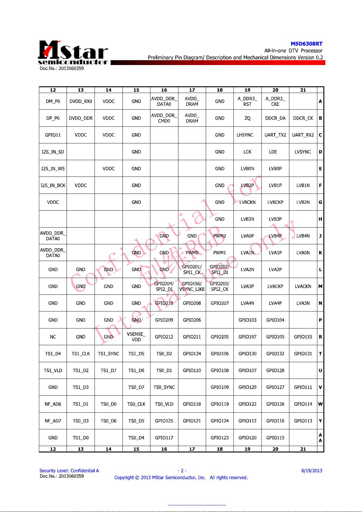
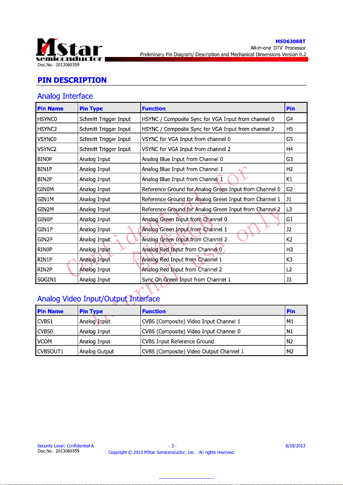
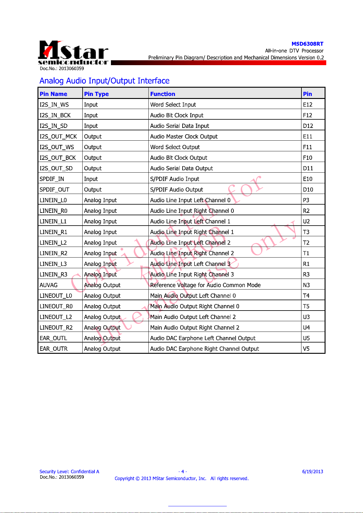
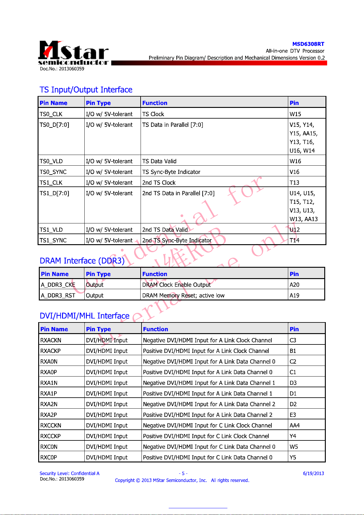
6 Terminals Configuration
6.1 Teminal Direction (Side and Bottom & Side and Rear)
6.2 Wifi Wifi
6.2.1 Tuner BackX2
6.2.2 Composite Side X1
6.2.3 S-Video No
6.2.4 Full Scart No
6.2.5 Half Scart No
6.2.6 Component Side X1
6.2.7 PC input with 3.5mm mini jack audio input Side X1(same AV audio)
6.2.8 HDMI Side X1 BackX1
6.2.9 USB Side X1
6.2.10 LAN Back X1
6.2.11 CI Slot No
6.2.12 CA Slot No
Page 6

6.3 Output Output
Power on / Standby / Recording(Green / Red / Orange)
\
6.3.1 Video Output No
6.3.2 Audio Output (Fixed & Variable) Share with earphone
6.3.3 Digital Audio Output (Coaxial & Optical) No
6.3.4 Earphone Back X1
6.4 Diagram of Teminal Configuration
7 Mechanical Spec
7.1 Cabinet Cabinet
7.1.1 Cabinet color For front back stand \
7.1.2 Operation Keys / Touch sensor
7.1.3 AC Power Switch Mechanical power switch \
7.1.4
LED Indicator
7.1.5 Power on / Standby (Green / Red ) \
7.1.6
7.1.7 Program Timer / Recoding (Green / Red) \
7.1.8 On Timer or Program Timer(Green) \
7.1.9 Logo Style Silk Printing / SUS Badge (inlet type) \
7.1.10 Stand Tilt / Swivel
7.2 Dimension & Stuffing Dimension & Stuffing
7.2.1 Size (with stand)( mm ) \
7.2.2 Size (without stand) ( mm ) \
7.2.3 Package Size (with stand)(mm) \
7.2.4 Net Weight(Kg) \
7.2.5 Gross Weight \
7.2.6 Loading quantity (20GP/40GP/40GP) with pallet \
7.2.7 Loading quantity (20GP/40GP/40GP) without pallet \
7.2.8 Stand build in Packing Box (together or separately ) \
8 Accessories
8.1 Remote Controller Remote Controller
8.1.1 Type No. TBD
8.1.2 Battery TBD
8.2 Instruction Manual Instruction Manual
8.2.1 Paper size \
8.2.2 Printing Color \
8.2.3 Languages (Refer to Sales Country Sheet) \
8.2.4 Total Pages \
8.2 Others Others
8.2.1 3D Glasses \
8.2.2 Camera \
8.2.3 etc \
9 Requested Certification
9.1 CB Yes
9.2 UL \
9.3 EMC TBD
9.4 FCC \
9.5 HDMI Yes
9.6 USB No
9.7 CI+ No
9.8 Dolby No
9.9 DOLBY + No
9.10 Dvix Hometheatre \
9.11 DviX HD \
9.12 DviX+HD \
9.13 MHL No
9.14 DLNA \
9.15 CTS \
9.16 Wifi \
9.17 MPES \
9.18 Energy Star \
Power on (Green) \
Please see attached
\
Page 7

6M83B关键件清单
长周期\关键件分类 物料编号 单机用量 位号
TUNER 5219-06033D-7V00 1 T1
MAIN CHIP 475C-M63085-3690 1 U9
Nand-FLASH 4701-T581G1-0480 1 U23
AMP 4722-T31130-0280 1 U15
DC/DC 5V 476A-M14950-0080 1 U5
DC/DC 1.15V 476A-M14950-0080 1 U4
DC/DC 3.3V 476A-M14940-0080 1 U2
LDO 3.3V 47DG-L11171-0030 1 U6
LDO 1.5V 47B6-A11174-0300 1 U3
P-MOS 47D9-M94350-0080 1 U11
Page 8
Page 9
Page 10
Page 11
Page 12
Page 13
Page 14
Page 15
Page 16
PDF 文件使用 "pdfFactory Pro" 试用版本创建 www.fineprint.cn
Page 17
PDF 文件使用 "pdfFactory Pro" 试用版本创建 www.fineprint.cn
Page 18
PDF 文件使用 "pdfFactory Pro" 试用版本创建 www.fineprint.cn
Page 19
PDF 文件使用 "pdfFactory Pro" 试用版本创建 www.fineprint.cn
Page 20
PDF 文件使用 "pdfFactory Pro" 试用版本创建 www.fineprint.cn
Page 21
PDF 文件使用 "pdfFactory Pro" 试用版本创建 www.fineprint.cn
Page 22
PDF 文件使用 "pdfFactory Pro" 试用版本创建 www.fineprint.cn
Page 23
PDF 文件使用 "pdfFactory Pro" 试用版本创建 www.fineprint.cn
Page 24
PDF 文件使用 "pdfFactory Pro" 试用版本创建 www.fineprint.cn
Page 25
PDF 文件使用 "pdfFactory Pro" 试用版本创建 www.fineprint.cn
Page 26
PDF 文件使用 "pdfFactory Pro" 试用版本创建 www.fineprint.cn
Page 27
PDF 文件使用 "pdfFactory Pro" 试用版本创建 www.fineprint.cn
Page 28
PDF 文件使用 "pdfFactory Pro" 试用版本创建 www.fineprint.cn
Page 29
PDF 文件使用 "pdfFactory Pro" 试用版本创建 www.fineprint.cn
Page 30
PDF 文件使用 "pdfFactory Pro" 试用版本创建 www.fineprint.cn
Page 31

PDF 文件使用 "pdfFactory Pro" 试用版本创建 www.fineprint.cn
Page 32

PDF 文件使用 "pdfFactory Pro" 试用版本创建 www.fineprint.cn
Page 33

www.ti.com
...........................................................................................................................................SLOS650B–AUGUST2009–REVISEDSEPTEMBER2009
6-WFILTER-FREESTEREOCLASS-DAUDIOPOWERAMPLIFIERWITH
1
FEATURES
2
•6-W/chintoan8-ΩLoadsat10%THD+NFrom
a10-VSupply
•12-Wintoa4-ΩMonoLoadat10%THD+N
Froma10-VSupply
•87%EfficientClass-DOperationEliminates
NeedforHeatSinks
•WideSupplyVoltageRangeAllowsOperation
from8Vto26V
•Filter-FreeOperation
•SpeakerGuard™SpeakerProtectionIncludes
AdjustablePowerLimiterplusDCProtection
•FlowThroughPinOutFacilitatesEasyBoard
Layout
•RobustPin-to-PinShortCircuitProtectionand
ThermalProtectionwithAutoRecoveryOption
•ExcellentTHD+N/Pop-FreePerformance
•FourSelectable,FixedGainSettings
•DifferentialInputs
APPLICATIONS
•Televisions
•ConsumerAudioEquipment
•Monitors
TPA3113D2
SPEAKERGUARD™
DESCRIPTION
TheTPA3113D2isa6-W(perchannel)efficient,
Class-Daudiopoweramplifierfordrivingbridged-tied
stereospeakers.AdvancedEMISuppression
Technologyenablestheuseofinexpensiveferrite
beadfiltersattheoutputswhilemeetingEMC
requirements.SpeakerGuard™speakerprotection
circuitryincludesanadjustablepowerlimiteranda
DCdetectioncircuit.Theadjustablepowerlimiter
allowstheusertoseta"virtual"voltageraillower
thanthechipsupplytolimittheamountofcurrent
throughthespeaker.TheDCdetectcircuitmeasures
thefrequencyandamplitudeofthePWMsignaland
shutsofftheoutputstageiftheinputcapacitorsare
damagedorshortsexistontheinputs.
TheTPA3113D2candrivestereospeakersaslowas
4Ω.ThehighefficiencyoftheTPA3113D2,87%,
eliminatestheneedforanexternalheatsinkwhen
playingmusic.
Theoutputsarealsofullyprotectedagainstshortsto
GND,VCC,andoutput-to-output.Theshort-circuit
protectionandthermalprotectionincludesan
auto-recoveryfeature.
OUTL+
Audio
Source
OUTL-
OUTR+
OUTR-
Figure1.TPA3113D2SimplifiedApplicationSchematic
1
Pleasebeawarethatanimportantnoticeconcerningavailability,standardwarranty,anduseincriticalapplicationsofTexas
Instrumentssemiconductorproductsanddisclaimerstheretoappearsattheendofthisdatasheet.
2SpeakerGuard,PowerPadaretrademarksofTexasInstruments.
PRODUCTIONDATAinformationiscurrentasofpublicationdate.
ProductsconformtospecificationsperthetermsoftheTexas
Instrumentsstandardwarranty.Productionprocessingdoesnot
necessarilyincludetestingofallparameters.
1 Fm
LINP
LINN
RINP
RINN
GAIN0
GAIN1
PLIMIT
PBTL
FaultFault
SDSD
TPA3113D2
OUTPL
OUTNL
OUTPR
OUTNR
PVCC
FERRITE
FERRITE
FERRITE
BEAD
BEAD
BEAD
FILTER
FILTER
FILTER
FERRITE
FERRITE
FERRITE
BEAD
BEAD
BEAD
FILTER
FILTER
FILTER
8to26V
Copyright©2009,TexasInstrumentsIncorporated
6W
6W
8W
8W
Page 34

TPA3113D2
SLOS650B–AUGUST2009–REVISEDSEPTEMBER2009...........................................................................................................................................
Thesedeviceshavelimitedbuilt-inESDprotection.Theleadsshouldbeshortedtogetherorthedeviceplacedinconductivefoam
duringstorageorhandlingtopreventelectrostaticdamagetotheMOSgates.
www.ti.com
ABSOLUTEMAXIMUMRATINGS
overoperatingfree-airtemperaturerange(unlessotherwisenoted)
V
V
T
T
T
R
ESDElectrostaticdischarge
(1)Stressesbeyondthoselistedunderabsolutemaximumratingsmaycausepermanentdamagetothedevice.Thesearestressratings
(2)TheTPA3113D2incorporatesanexposedthermalpadontheundersideofthechip.Thisactsasaheatsink,anditmustbeconnected
(3)InaccordancewithJEDECStandard22,TestMethodA114-B.
(4)InaccordancewithJEDECStandard22,TestMethodC101-A
SupplyvoltageAVCC,PVCC–0.3Vto30V
CC
SD,GAIN0,GAIN1,PBTL,FAULT
InterfacepinvoltagePLIMIT–0.3VtoGVDD+0.3V
I
RINN,RINP,LINN,LINP–0.3Vto6.3V
ContinuoustotalpowerdissipationSeeDissipationRatingTable
Operatingfree-airtemperaturerange–40°Cto85°C
A
Operatingjunctiontemperaturerange
J
Storagetemperaturerange–65°Cto150°C
stg
(2)
BTL:PVCC>15V4.8
MinimumLoadResistanceBTL:PVCC≤15V3.2
L
PBTL3.2
Humanbodymodel
Charged-devicemodel
(3)
(allpins)±2kV
(4)
only,andfunctionaloperationsofthedeviceattheseoranyotherconditionsbeyondthoseindicatedunderrecommendedoperating
conditionsisnotimplied.Exposuretoabsolute-maximum-ratedconditionsforextendedperiodsmayaffectdevicereliability.
toathermallydissipatingplaneforproperpowerdissipation.Failuretodosomayresultinthedevicegoingintothermalprotection
shutdown.SeeTITechnicalBriefsSLMA002formoreinformationaboutusingtheTSSOPthermalpad.
(1)
UNIT
–0.3VtoV
–40°Cto150°C
(allpins)±500V
+0.3V
CC
DISSIPATIONRATINGS
PACKAGE
28pinTSSOP(PWP)4.48W27.87°C/W2.33W0.72°C/W0.45°C/W
(1)Forthemostcurrentpackageandorderinginformation,seethePackageOptionAddendumattheendofthisdocument,orseetheTI
websiteatwww.ti.com.
(1)
TA≤25°CDERATINGFACTOR(θJA)TA=85°Cθ
JP
Ψ
JT
RECOMMENDEDOPERATINGCONDITIONS
overoperatingfree-airtemperaturerange(unlessotherwisenoted)
PARAMETERTESTCONDITIONSMINMAXUNIT
V
V
V
V
I
I
T
SupplyvoltagePVCC,AVCC826V
CC
High-levelinputvoltageSD,GAIN0,GAIN1,PBTL2V
IH
Low-levelinputvoltageSD,GAIN0,GAIN1,PBTL0.8V
IL
Low-leveloutputvoltageFAULT,R
OL
High-levelinputcurrentSD,GAIN0,GAIN1,PBTL,VI=2V,V
IH
Low-levelinputcurrentSD,GAIN0,GAIN1,PBTL,VI=0.8V,V
IL
Operatingfree-airtemperature–4085°C
A
=100k,VCC=26V0.8V
PULL-UP
=18V50µA
CC
=18V5µA
CC
2SubmitDocumentationFeedbackCopyright©2009,TexasInstrumentsIncorporated
ProductFolderLink(s):TPA3113D2
Page 35

www.ti.com
...........................................................................................................................................SLOS650B–AUGUST2009–REVISEDSEPTEMBER2009
DCCHARACTERISTICS
TA=25°C,V
|V
|VI=0V,Gain=36dB1.515mV
OS
I
CC
I
CC(SD)
r
DS(on)
GGain
t
on
t
OFF
GVDDGateDriveSupplyI
t
DCDET
=24V,RL=8Ω(unlessotherwisenoted)
CC
PARAMETERTESTCONDITIONSMINTYPMAXUNIT
Class-Doutputoffsetvoltage(measured
differentially)
QuiescentsupplycurrentSD=2V,noload,PV
QuiescentsupplycurrentinshutdownmodeSD=0.8V,noload,PV
V
=12V,IO=500mA,
Drain-sourceon-stateresistancemΩ
CC
TJ=25°C
GAIN1=0.8VdB
GAIN1=2VdB
=24V3250mA
CC
=24V250400µA
CC
HighSide400
Lowside400
GAIN0=0.8V192021
GAIN0=2V252627
GAIN0=0.8V313233
GAIN0=2V353637
Turn-ontimeSD=2V
Turn-offtimeSD=0.8V2µs
=100µA6.46.97.4V
GVDD
DCDetecttimeV
=6V,VRINP=0V420ms
(RINN)
DCCHARACTERISTICS
TA=25°C,V
|V
|VI=0V,Gain=36dB1.515mV
OS
I
CC
I
CC(SD)
r
DS(on)
GGain
t
ON
t
OFF
GVDDGateDriveSupplyI
V
O
=12V,RL=8Ω(unlessotherwisenoted)
CC
PARAMETERTESTCONDITIONSMINTYPMAXUNIT
Class-Doutputoffsetvoltage(measured
differentially)
QuiescentsupplycurrentSD=2V,noload,PV
QuiescentsupplycurrentinshutdownmodeSD=0.8V,noload,PV
V
=12V,IO=500mA,
Drain-sourceon-stateresistancemΩ
CC
TJ=25°C
GAIN1=0.8VdB
GAIN1=2VdB
=12V2035mA
CC
=12V200µA
CC
HighSide400
Lowside400
GAIN0=0.8V192021
GAIN0=2V252627
GAIN0=0.8V313233
GAIN0=2V353637
Turn-ontimeSD=2V
Turn-offtimeSD=0.8V2µs
=2mA6.46.97.4V
GVDD
OutputVoltagemaximumunderPLIMIT
control
V
=2V;VI=1Vrms6.757.908.75V
(PLIMIT)
TPA3113D2
14ms
14ms
Copyright©2009,TexasInstrumentsIncorporatedSubmitDocumentationFeedback3
ProductFolderLink(s):TPA3113D2
Page 36

TPA3113D2
SLOS650B–AUGUST2009–REVISEDSEPTEMBER2009...........................................................................................................................................
ACCHARACTERISTICS
TA=25°C,V
K
SVR
P
O
THD+NTotalharmonicdistortion+noiseV
V
n
SNRSignal-to-noiseratio102dB
f
OSC
=24V,RL=8Ω(unlessotherwisenoted)
CC
PARAMETERTESTCONDITIONSMINTYPMAXUNIT
PowerSupplyripplerejection–70dB
200mV
Gain=20dB,Inputsac-coupledtoAGND
ContinuousoutputpowerTHD+N=10%,f=1kHz,V
CC
Outputintegratednoise20Hzto22kHz,A-weightedfilter,Gain=20dB
rippleat1kHz,
PP
=10V6W
CC
=16V,f=1kHz,PO=3W(half-power)0.07%
65µV
–80dBV
CrosstalkVO=1Vrms,Gain=20dB,f=1kHz–100dB
MaximumoutputatTHD+N<1%,f=1kHz,
Gain=20dB,A-weighted
Oscillatorfrequency250310350kHz
Thermaltrippoint150°C
Thermalhysteresis15°C
ACCHARACTERISTICS
TA=25°C,V
K
SVR
THD+NTotalharmonicdistortion+noiseRL=8Ω,f=1kHz,PO=3W(half-power)0.06%
V
n
SNRSignal-to-noiseratio102dB
f
OSC
=12V,RL=8Ω(unlessotherwisenoted)
CC
PARAMETERTESTCONDITIONSMINTYPMAXUNIT
Supplyripplerejection–70dB
200mV
Gain=20dB,Inputsac-coupledtoAGND
Outputintegratednoise20Hzto22kHz,A-weightedfilter,Gain=20dB
ripplefrom20Hz–1kHz,
PP
65µV
–80dBV
CrosstalkPo=1W,Gain=20dB,f=1kHz–100dB
MaximumoutputatTHD+N<1%,f=1kHz,
Gain=20dB,A-weighted
Oscillatorfrequency250310350kHz
Thermaltrippoint150°C
Thermalhysteresis15°C
www.ti.com
PWP(TSSOP)PACKAGE
(TOPVIEW)
SD
FAULT
LINP
LINN
GAIN0
GAIN1
AVCC
AGND
GVDD
PLIMIT
RINN
RINP
NC
PBTL
1
2
3
4
5
6
7
8
9
10
11
12
13
14
28
27
26
25
24
23
22
21
20
19
18
17
16
15
PVCCL
PVCCL
BSPL
OUTPL
PGND
OUTNL
BSNL
BSNR
OUTNR
PGND
OUTPR
BSPR
PVCCR
PVCCR
4SubmitDocumentationFeedbackCopyright©2009,TexasInstrumentsIncorporated
ProductFolderLink(s):TPA3113D2
Page 37

www.ti.com
...........................................................................................................................................SLOS650B–AUGUST2009–REVISEDSEPTEMBER2009
PINFUNCTIONS
PIN
NAME
SD
FAULT2O
LINP3IPositiveaudioinputforleftchannel.Biasedat3V.
LINN4INegativeaudioinputforleftchannel.Biasedat3V.
GAIN05IGainselectleastsignificantbit.TTLlogiclevelswithcompliancetoAVCC.
GAIN16IGainselectmostsignificantbit.TTLlogiclevelswithcompliancetoAVCC.
AVCC7PAnalogsupply
AGND8Analogsignalground.Connecttothethermalpad.
GVDD9O
PLIMIT10I
RINN11INegativeaudioinputforrightchannel.Biasedat3V.
RINP12IPositiveaudioinputforrightchannel.Biasedat3V.
NC13Notconnected
PBTL14IParallelBTLmodeswitch
PVCCR15P
PVCCR16P
BSPR17IBootstrapI/Oforrightchannel,positivehigh-sideFET.
OUTPR18OClass-DH-bridgepositiveoutputforrightchannel.
PGND19PowergroundfortheH-bridges.
OUTNR20OClass-DH-bridgenegativeoutputforrightchannel.
BSNR21IBootstrapI/Oforrightchannel,negativehigh-sideFET.
BSNL22IBootstrapI/Oforleftchannel,negativehigh-sideFET.
OUTNL23OClass-DH-bridgenegativeoutputforleftchannel.
PGND24PowergroundfortheH-bridges.
OUTPL25OClass-DH-bridgepositiveoutputforleftchannel.
BSPL26IBootstrapI/Oforleftchannel,positivehigh-sideFET.
PVCCL27P
PVCCL28P
Pin
Number
1I
I/O/PDESCRIPTION
Shutdownlogicinputforaudioamp(LOW=outputsHi-Z,HIGH=outputs
enabled).TTLlogiclevelswithcompliancetoAVCC.
Opendrainoutputusedtodisplayshortcircuitordcdetectfaultstatus.Voltage
complianttoAVCC.Shortcircuitfaultscanbesettoauto-recoverybyconnecting
FAULTpintoSDpin.Otherwise,bothshortcircuitfaultsanddcdetectfaultsmust
beresetbycyclingPVCC.
High-sideFETgatedrivesupply.Nominalvoltageis7V.Alsoshouldbeusedas
supplyforPLIMITfunction
Powerlimitleveladjust.ConnectaresistordividerfromGVDDtoGNDtoset
powerlimit.ConnectdirectlytoGVDDfornopowerlimit.
PowersupplyforrightchannelH-bridge.Rightchannelandleftchannelpower
supplyinputsareconnectinternally.
PowersupplyforrightchannelH-bridge.Rightchannelandleftchannelpower
supplyinputsareconnectinternally.
PowersupplyforleftchannelH-bridge.Rightchannelandleftchannelpower
supplyinputsareconnectinternally.
PowersupplyforleftchannelH-bridge.Rightchannelandleftchannelpower
supplyinputsareconnectinternally.
TPA3113D2
Copyright©2009,TexasInstrumentsIncorporatedSubmitDocumentationFeedback5
ProductFolderLink(s):TPA3113D2
Page 38

TPA3113D2
SLOS650B–AUGUST2009–REVISEDSEPTEMBER2009...........................................................................................................................................
FUNCTIONALBLOCKDIAGRAM
www.ti.com
LINP
LINN
FAULT
GAIN0
GAIN1
PLIMIT
AVCC
GVDD
RINN
RINP
GVDD
PVCCL
PBTL Select
Gate
Drive
OUTPL FB
Logic
PWM
Logic
PWM
Logic
SC Detect
DC Detect
Thermal
Detect
UVLO/OVLO
PVCCL
PVCCL
PVCCL
Gate
Drive
Gate
Drive
GVDD
GVDD
GVDD
Gain
Control
OUTNL FB
SD
TTL
Buffer
LDO
Regulator
OUTNN FB
Gain
Control
OUTNP FB
Gain
Control
AVDD
GVDD
PLIMIT
Reference
Ramp
Generator
PLIMIT
PLIMIT
Biases and
References
Startup Protection
PVCCL
PVCCL
PVCCL
PVCCL
BSPL
OUTPL FB
OUTPL
PGND
BSNL
OUTNL FB
OUTNL
PGND
BSNR
OUTNR
OUTNR FB
PGND
BSPR
AGND
PBTL
TTL
Buffer
PBTL
Select
PBTL Select
Gate
Drive
OUTPR
OUTPR FB
PGND
6SubmitDocumentationFeedbackCopyright©2009,TexasInstrumentsIncorporated
ProductFolderLink(s):TPA3113D2
Page 39

TPA3113D2
www.ti.com
(AllMeasurementstakenat1kHz,unlessotherwisenoted.MeasurementsweremadeusingtheTPA3113D2EVMwhichis
...........................................................................................................................................SLOS650B–AUGUST2009–REVISEDSEPTEMBER2009
TYPICALCHARACTERISTICS
availableatti.com.)
TOTALHARMONICDISTORTIONTOTALHARMONICDISTORTION
vsvs
FREQUENCY(BTL)FREQUENCY(BTL)
10
Gain = 20 dB
VCC = 12 V
ZL = 8 Ω + 66 µH
1
0.1
PO = 5 W
0.01
PO = 0.5 W
THD − Total Harmonic Distortion − %
PO = 2.5 W
0.001
20 100 1k 10k
f − Frequency − Hz
Figure2.Figure3.
TOTALHARMONICDISTORTIONTOTALHARMONICDISTORTION
vsvs
FREQUENCY(BTL)FREQUENCY(BTL)
10
Gain=20dB
VCC=24V
=8 W +66 Hm
Z
− %
L
1
20k
10
− %
0.1
otalHarmonicDistortion
0.01
THD − T
0.001
G001
10
Gain=20dB
VCC=18V
Z
=8 W +66 Hm
L
1
PO=1W
PO=5W
20 100 1k 10k
f − Frequency − Hz
Gain = 20 dB
VCC = 12 V
ZL = 6 Ω + 47 µH
1
20k
G002
0.1
otalHarmonicDistortion
0.01
THD − T
PO=1W
0.1
PO = 5 W
0.01
THD − Total Harmonic Distortion − %
PO = 0.5 W
PO = 2.5 W
PO=5W
0.001
20 100 1k 10k
f − Frequency − Hz
20k
G003
0.001
20 100 1k 10k
f − Frequency − Hz
20k
Figure4.Figure5.
Copyright©2009,TexasInstrumentsIncorporatedSubmitDocumentationFeedback7
ProductFolderLink(s):TPA3113D2
G004
Page 40

TPA3113D2
SLOS650B–AUGUST2009–REVISEDSEPTEMBER2009...........................................................................................................................................
TYPICALCHARACTERISTICS(continued)
(AllMeasurementstakenat1kHz,unlessotherwisenoted.MeasurementsweremadeusingtheTPA3113D2EVMwhichis
availableatti.com.)
www.ti.com
TOTALHARMONICDISTORTIONTOTALHARMONICDISTORTION
vsvs
FREQUENCY(BTL)FREQUENCY(BTL)
10
Gain=20dB
VCC=18V
Z
=6 W +47 Hm
L
1
0.1
0.01
THD − TotalHarmonicDistortion − %
PO=1W
PO=5W
0.001
20 100 1k 10k
f − Frequency − Hz
Figure6.Figure7.
TOTALHARMONICDISTORTION+NOISETOTALHARMONICDISTORTION+NOISE
vsvs
OUTPUTPOWER(BTL)OUTPUTPOWER(BTL)
10
Gain = 20 dB
VCC = 12 V
ZL = 8 Ω + 66 µH
1
20k
10
− %
0.1
0.01
THD − TotalHarmonicDistortion
0.001
G005
10
Gain=20dB
VCC=12V
Z
=4 W +33 Hm
L
1
PO=1W
PO=5W
20 100 1k 10k
f − Frequency − Hz
Gain = 20 dB
VCC = 18 V
ZL = 8 Ω + 66 µH
1
20k
G006
0.1
f = 1 kHz
0.01
THD+N − Total Harmonic Distortion + Noise − %
0.001
0.01 0.1 1
PO − Output Power − W
f = 20 Hz
f = 10 kHz
10
0.1
0.01
THD+N − Total Harmonic Distortion + Noise − %
0.001
0.01 0.1 1 10
G007
f = 1 kHz
f = 10 kHz
PO − Output Power − W
f = 20 Hz
Figure8.Figure9.
8SubmitDocumentationFeedbackCopyright©2009,TexasInstrumentsIncorporated
ProductFolderLink(s):TPA3113D2
G008
Page 41

TPA3113D2
www.ti.com
(AllMeasurementstakenat1kHz,unlessotherwisenoted.MeasurementsweremadeusingtheTPA3113D2EVMwhichis
availableatti.com.)
...........................................................................................................................................SLOS650B–AUGUST2009–REVISEDSEPTEMBER2009
TYPICALCHARACTERISTICS(continued)
TOTALHARMONICDISTORTION+NOISETOTALHARMONICDISTORTION+NOISE
vsvs
OUTPUTPOWER(BTL)OUTPUTPOWER(BTL)
10
Gain = 20 dB
VCC = 24 V
ZL = 8 Ω + 66 µH
1
f = 1 kHz
0.1
0.01
f = 20 Hz
THD+N − Total Harmonic Distortion + Noise − %
f = 10 kHz
0.001
0.01 0.1 1 10
PO − Output Power − W
Figure10.Figure11.
TOTALHARMONICDISTORTION+NOISETOTALHARMONICDISTORTION+NOISE
vsvs
OUTPUTPOWER(BTL)OUTPUTPOWER(BTL)
10
Gain = 20 dB
VCC = 18 V
ZL = 6 Ω + 47 µH
1
10
Gain = 20 dB
VCC = 12 V
ZL = 6 Ω + 47 µH
1
0.1
0.01
THD+N − Total Harmonic Distortion + Noise − %
f = 10 kHz
0.001
0.01 0.1 1 10
G009
10
Gain = 20 dB
VCC = 12 V
ZL = 4 Ω + 33 µH
1
f = 1 kHz
f = 20 Hz
PO − Output Power − W
G010
f = 1 kHz
0.1
f = 20 Hz
0.01
THD+N − Total Harmonic Distortion + Noise − %
f = 10 kHz
0.001
0.01 0.1 1 10
PO − Output Power − W
0.1
0.01
THD+N − Total Harmonic Distortion + Noise − %
0.001
0.01 0.1 1 10
G011
f = 20 Hz
PO − Output Power − W
f = 1 kHz
f = 10 kHz
Figure12.Figure13.
Copyright©2009,TexasInstrumentsIncorporatedSubmitDocumentationFeedback9
ProductFolderLink(s):TPA3113D2
G012
Page 42

TPA3113D2
SLOS650B–AUGUST2009–REVISEDSEPTEMBER2009...........................................................................................................................................
TYPICALCHARACTERISTICS(continued)
(AllMeasurementstakenat1kHz,unlessotherwisenoted.MeasurementsweremadeusingtheTPA3113D2EVMwhichis
availableatti.com.)
www.ti.com
MAXIMUMOUTPUTPOWEROUTPUTPOWER
vsvs
PLIMITVOLTAGE(BTL)PLIMITVOLTAGE(BTL)
16
Gain = 20 dB
VCC = 24 V
14
ZL = 8 Ω + 66 µH
12
35
Gain = 20 dB
VCC = 12 V
30
ZL = 4 Ω + 33 µH
25
10
20
8
15
6
− Maximum Output Power − W
4
O(Max)
P
2
0
0.0 0.5 1.0 1.5 2.0 2.5 3.0
V
− PLIMIT Voltage − V
PLIMIT
− Output Power − W
O
P
G013
10
5
0
0 1 2 3 4 5 6
V
− PLIMIT Voltage − V
PLIMIT
Note:DashedlinerepresentsthermallylimitedNote:Dashedlinerepresentsthermallylimited
region.region.
Figure14.Figure15.
G014
GAIN/PHASEEFFICIENCY
vsvs
FREQUENCY(BTL)OUTPUTPOWER(BTL)
40
35
30
25
20
Gain − dB
15
CI = 1 µF
Gain = 20 dB
10
Filter = Audio Precision AUX-0025
VCC = 12 V
5
VI = 0.1 Vrms
ZL = 8 Ω + 66 µH
0
20 100 10k 100k
Phase
Gain
1k
f − Frequency − Hz
Figure16.
100
50
0
−50
−100
−150
−200
−250
−300
100
90
80
70
60
50
Phase − °
40
η − Efficiency − %
30
20
10
0
G015
0 1 2 3 4 5 6 7 8 9 10
PO − Output Power − W
Note:Dashedlinesrepresentthermallylimited
region.
VCC = 12 V
VCC = 18 V
VCC = 24 V
Gain = 20 dB
ZL = 8 Ω + 66 µH
G018
Figure17.
10SubmitDocumentationFeedbackCopyright©2009,TexasInstrumentsIncorporated
ProductFolderLink(s):TPA3113D2
Page 43

TPA3113D2
www.ti.com
(AllMeasurementstakenat1kHz,unlessotherwisenoted.MeasurementsweremadeusingtheTPA3113D2EVMwhichis
availableatti.com.)
...........................................................................................................................................SLOS650B–AUGUST2009–REVISEDSEPTEMBER2009
TYPICALCHARACTERISTICS(continued)
EFFICIENCYEFFICIENCY
OUTPUTPOWER(BTLwithLCFILTER)OUTPUTPOWER(BTL)
100
vsvs
100
90
80
70
60
50
40
η − Efficiency − %
30
20
10
0
0 1 2 3 4 5 6 7 8 9 10
VCC = 12 V
VCC = 24 V
Gain = 20 dB
LC Filter = 22 µH + 0.68 µF
RL = 8 Ω
PO − Output Power − W
VCC = 18 V
G032
90
VCC = 12 V
80
70
60
50
40
η − Efficiency − %
30
20
10
0
0 1 2 3 4 5 6 7 8 9 10
PO − Output Power − W
Note:DashedlinesrepresentthermallylimitedNote:Dashedlinesrepresentthermallylimited
region.region.
Figure18.Figure19.
EFFICIENCYEFFICIENCY
vsvs
OUTPUTPOWER(BTLwithLCFILTER)OUTPUTPOWER(BTL)
100
90
80
70
VCC = 12 V
VCC = 18 V
100
90
80
70
Gain = 20 dB
VCC = 12 V
ZL = 4 Ω + 33 µH
VCC = 18 V
Gain = 20 dB
ZL = 6 Ω + 47 µH
G019
60
50
40
η − Efficiency − %
30
20
10
Gain = 20 dB
LC Filter = 22 µH + 0.68 µF
RL = 6 Ω
0
0 1 2 3 4 5 6 7 8 9 10
PO − Output Power − W
G033
60
50
40
η − Efficiency − %
30
20
10
0
0 1 2 3 4 5 6 7 8 9 10
PO − Output Power − W
Note:DashedlinesrepresentthermallylimitedNote:Dashedlinerepresentsthermallylimited
region.region.
Figure20.Figure21.
Copyright©2009,TexasInstrumentsIncorporatedSubmitDocumentationFeedback11
ProductFolderLink(s):TPA3113D2
G020
Page 44

TPA3113D2
SLOS650B–AUGUST2009–REVISEDSEPTEMBER2009...........................................................................................................................................
TYPICALCHARACTERISTICS(continued)
(AllMeasurementstakenat1kHz,unlessotherwisenoted.MeasurementsweremadeusingtheTPA3113D2EVMwhichis
availableatti.com.)
EFFICIENCYSUPPLYCURRENT
OUTPUTPOWER(BTLwithLCFILTER)TOTALOUTPUTPOWER(BTL)
100
90
80
vsvs
1.2
Gain = 20 dB
ZL = 8 Ω + 66 µH
1.0
www.ti.com
70
0.8
VCC = 12 V
60
50
0.6
VCC = 18 V
40
η − Efficiency − %
30
20
10
Gain = 20 dB
LC Filter = 22 µH + 0.68 µF
RL = 4 Ω
0
0 1 2 3 4 5 6 7 8 9 10
PO − Output Power − W
− Supply Current − A
CC
I
G034
0.4
0.2
0.0
0 1 2 3 4 5 6 7 8 9 10
P
− Total Output Power − W
O(Tot)
Note:DashedlinerepresentsthermallylimitedNote:Dashedlinesrepresentthermallylimited
region.region.
Figure22.Figure23.
CROSSTALKSUPPLYRIPPLEREJECTIONRATIO
vsvs
FREQUENCY(BTL)FREQUENCY(BTL)
−20
−30
−40
Gain = 20 dB
VCC = 12 V
VO = 1 Vrms
ZL = 8 Ω + 66 µH
0
−20
Gain = 20 dB
V
= 200 mV
ripple
ZL = 8 Ω + 66 µH
pp
−50
−60
−40
VCC = 24 V
G021
−70
−80
Crosstalk − dB
−90
−60
Right to Left
−80
VCC = 12 V
−100
−110
Left to Right
−120
−130
20 100 1k 10k 20k
f − Frequency − Hz
− Supply Ripple Rejection Ratio − dB
−100
SVR
K
−120
20 100 1k 10k 20k
G023
f − Frequency − Hz
Figure24.Figure25.
12SubmitDocumentationFeedbackCopyright©2009,TexasInstrumentsIncorporated
ProductFolderLink(s):TPA3113D2
G024
Page 45

TPA3113D2
www.ti.com
(AllMeasurementstakenat1kHz,unlessotherwisenoted.MeasurementsweremadeusingtheTPA3113D2EVMwhichis
availableatti.com.)
...........................................................................................................................................SLOS650B–AUGUST2009–REVISEDSEPTEMBER2009
TYPICALCHARACTERISTICS(continued)
TOTALHARMONICDISTORTIONTOTALHARMONICDISTORTION+NOISE
vsvs
FREQUENCY(PBTL)OUTPUTPOWER(PBTL)
10
Gain=20dB
VCC=12V
Z
=4 W +33 Hm
L
1
PO=5W
0.1
0.01
THD − TotalHarmonicDistortion − %
PO=2.5W
0.001
20 100 1k 10k
f − Frequency − Hz
Figure26.Figure27.
GAIN/PHASEEFFICIENCY
vsvs
FREQUENCY(PBTL)OUTPUTPOWER(PBTL)
40
35
30
25
20
Gain − dB
15
CI = 1 µF
Gain = 20 dB
10
Filter = Audio Precision AUX-0025
VCC = 24 V
5
VI = 0.1 Vrms
ZL = 8 Ω + 66 µH
0
20 100 10k 100k1k
Phase
Gain
f − Frequency − Hz
Figure28.Figure29.
PO=0.5W
20k
100
50
0
−50
−100
−150
−200
−250
−300
G025
G027
TotalHarmonicDistortion+Noise − %
THD+N −
0.001
Phase − °
η − Efficiency − %
10
Gain=20dB
VCC=12V
Z
=4 W +33 Hm
L
1
f=1kHz
0.1
0.01
f=20Hz
f=10kHz
0.01 0.1 1 10
PO− OutputPower − W
100
90
80
VCC = 12 V
VCC = 18 V
70
60
50
40
30
20
10
Gain = 20 dB
ZL = 4 Ω + 33 µH
0
0 1 2 3 4 5 6 7 8 9 10
PO − Output Power − W
50
G026
G029
Copyright©2009,TexasInstrumentsIncorporatedSubmitDocumentationFeedback13
ProductFolderLink(s):TPA3113D2
Page 46

TPA3113D2
SLOS650B–AUGUST2009–REVISEDSEPTEMBER2009...........................................................................................................................................
TYPICALCHARACTERISTICS(continued)
(AllMeasurementstakenat1kHz,unlessotherwisenoted.MeasurementsweremadeusingtheTPA3113D2EVMwhichis
availableatti.com.)
www.ti.com
SUPPLYCURRENTSUPPLYRIPPLEREJECTIONRATIO
vsvs
OUTPUTPOWER(PBTL)FREQUENCY(PBTL)
1.0
Gain = 20 dB
0.9
ZL = 4 Ω + 33 µH
0.8
0.7
0.6
VCC = 12 V
0.5
0.4
− Supply Current − A
0.3
CC
I
VCC = 18 V
0.2
0.1
0.0
0 1 2 3 4 5 6 7 8 9 10
PO − Output Power − W
Figure30.Figure31.
0
Gain = 20 dB
V
= 200 mV
ripple
ZL = 8 Ω + 66 µH
−20
−40
−60
−80
− Supply Ripple Rejection Ratio − dB
−100
SVR
K
−120
20 100 1k 10k 20k
G030
pp
VCC = 12 V
f − Frequency − Hz
G031
14SubmitDocumentationFeedbackCopyright©2009,TexasInstrumentsIncorporated
ProductFolderLink(s):TPA3113D2
Page 47

TPA3113D2
www.ti.com
GainSettingViaGAIN0andGAIN1Inputs
ThegainoftheTPA3113D2issetbytwoinputterminals,GAIN0andGAIN1.
ThegainslistedinTable1arerealizedbychangingthetapsontheinputresistorsandfeedbackresistorsinside
theamplifier.Thiscausestheinputimpedance(Z
arecontrolledbyratiosofresistors,sothegainvariationfrompart-to-partissmall.However,theinputimpedance
frompart-to-partatthesamegainmayshiftby±20%duetoshiftsintheactualresistanceoftheinputresistors.
Fordesignpurposes,theinputnetwork(discussedinthenextsection)shouldbedesignedassuminganinput
impedanceof7.2kΩ,whichistheabsoluteminimuminputimpedanceoftheTPA3113D2.Atthelowergain
settings,theinputimpedancecouldincreaseashighas72kΩ
...........................................................................................................................................SLOS650B–AUGUST2009–REVISEDSEPTEMBER2009
DEVICEINFORMATION
)tobedependentonthegainsetting.Theactualgainsettings
I
Table1.GainSetting
GAIN1GAIN0
002060
012630
103215
11369
AMPLIFIERGAIN(dB)
TYPTYP
INPUTIMPEDANCE
(kΩ)
SDOperation
TheTPA3113D2employsashutdownmodeofoperationdesignedtoreducesupplycurrent(I
minimumlevelduringperiodsofnonuseforpowerconservation.TheSDinputterminalshouldbeheldhigh(see
specificationtablefortrippoint)duringnormaloperationwhentheamplifierisinuse.PullingSDlowcausesthe
outputstomuteandtheamplifiertoenteralow-currentstate.NeverleaveSDunconnected,becauseamplifier
operationwouldbeunpredictable.
Forthebestpower-offpopperformance,placetheamplifierintheshutdownmodepriortoremovingthepower
supplyvoltage.
)totheabsolute
CC
PLIMIT
Thevoltageatpin10canusedtolimitthepowertolevelsbelowthatwhichispossiblebasedonthesupplyrail.
AddaresistordividerfromGVDDtogroundtosetthevoltageatthePLIMITpin.Anexternalreferencemayalso
beusediftightertoleranceisrequired.Alsoadda1µFcapacitorfrompin10toground.
Vinput
PLIMIT =6.96VPout=11.8W
PLIMIT =3VPout=10W
PLIMIT =1.8VPout=5W
TPA3110D1PowerLimitFunction
Vin=1.13 Freq=1kHzRLoad=8WV
PP
Figure32.PLIMITCircuitOperation
Copyright©2009,TexasInstrumentsIncorporatedSubmitDocumentationFeedback15
ProductFolderLink(s):TPA3113D2
Page 48

TPA3113D2
SLOS650B–AUGUST2009–REVISEDSEPTEMBER2009...........................................................................................................................................
ThePLIMITcircuitsetsalimitontheoutputpeak-to-peakvoltage.Thelimitingisdonebylimitingthedutycycle
tofixedmaximumvalue.Thislimitcanbethoughtofasa"virtual"voltagerailwhichislowerthanthesupply
connectedtoPVCC.This"virtual"railis4timesthevoltageatthePLIMITpin.Thisoutputvoltagecanbeusedto
calculatethemaximumoutputpowerforagivenmaximuminputvoltageandspeakerimpedance.
æ ö
æ ö
R
ç ÷
ç ÷
ç ÷
è ø
P = for unclipped power
OUT
è ø
L
R + 2 x R
L S
2 x R
L
x V
2
P
Where:
R
isthetotalseriesresistanceincludingR
S
R
istheloadresistance.
L
V
isthepeakamplitudeoftheoutputpossiblewithinthesupplyrail.
P
V
=4×PLIMITvoltageifPLIMIT<4×V
P
P
(10%THD)=1.25×P
OUT
(unclipped)
OUT
,andanyresistanceintheoutputfilter.
DS(on)
P
Table2.PLIMITTypicalOperation
TESTCONDITIONS()PLIMITVOLTAGE
PVCC=24V,Vin=1Vrms,1.62514
RL=8Ω,Gain=26dB
PVCC=24V,Vin=1Vrms,1.86514.8
RL=8Ω,Gain=20dB
PVCC=12V,Vin=1Vrms,1.76515
RL=8Ω,Gain=20dB
OUTPUTPOWEROUTPUTVOLTAGEAMPLITUDE
(W)(V
)
P-P
www.ti.com
(1)
GVDDSupply
TheGVDDSupplyisusedtopowerthegatesoftheoutputfullbridgetransistors.Itcanalsobeusedtosupply
thePLIMITvoltagedividercircuit.Adda1µFcapacitortogroundatthispin.
DCDetect
TPA3113D2hascircuitrywhichwillprotectthespeakersfromDCcurrentwhichmightoccurduetodefective
capacitorsontheinputorshortsontheprintedcircuitboardattheinputs.ADCdetectfaultwillbereportedon
theFAULTpinasalowstate.TheDCDetectfaultwillalsocausetheamplifiertoshutdownbychangingthe
stateoftheoutputstoHi-Z.TocleartheDCDetectitisnecessarytocyclethePVCCsupply.CyclingSDwill
NOTclearaDCdetectfault.
ADCDetectFaultisissuedwhentheoutputdifferentialduty-cycleofeitherchannelexceeds14%(forexample,
+57%,-43%)formorethan420msecatthesamepolarity.ThisfeatureprotectsthespeakerfromlargeDC
currentsorACcurrentslessthan2Hz.ToavoidnuisancefaultsduetotheDCdetectcircuit,holdtheSDpinlow
atpower-upuntilthesignalsattheinputsarestable.Also,takecaretomatchtheimpedanceseenatthepositive
andnegativeinputstoavoidnuisanceDCdetectfaults.
TheminimumdifferentialinputvoltagesrequiredtotriggertheDCdetectareshowintable2.Theinputsmust
remainatorabovethevoltagelistedinthetableformorethan420msectotriggertheDCdetect.
16SubmitDocumentationFeedbackCopyright©2009,TexasInstrumentsIncorporated
ProductFolderLink(s):TPA3113D2
Page 49

TPA3113D2
www.ti.com
PBTLSelect
TPA3113D2offersthefeatureofparallelBTLoperationwithtwooutputsofeachchannelconnecteddirectly.If
thePBTLpin(pin14)istiedhigh,thepositiveandnegativeoutputsofeachchannel(leftandright)are
synchronizedandinphase.TooperateinthisPBTL(mono)mode,applytheinputsignaltotheRIGHTinputand
placethespeakerbetweentheLEFTandRIGHToutputs.Connectthepositiveandnegativeoutputtogetherfor
bestefficiency.ForanexampleofthePBTLconnection,seetheschematicintheAPPLICATIONINFORMATION
section.
FornormalBTLoperation,connectthePBTLpintolocalground.
Short-CircuitProtectionandAutomaticRecoveryFeature
TPA3113D2hasprotectionfromovercurrentconditionscausedbyashortcircuitontheoutputstage.Theshort
circuitprotectionfaultisreportedontheFAULTpinasalowstate.TheamplifieroutputsareswitchedtoaHi-Z
statewhentheshortcircuitprotectionlatchisengaged.ThelatchcanbeclearedbycyclingtheSDpinthrough
thelowstate.
Ifautomaticrecoveryfromtheshortcircuitprotectionlatchisdesired,connecttheFAULTpindirectlytotheSD
pin.ThisallowstheFAULTpinfunctiontoautomaticallydrivetheSDpinlowwhichclearstheshort-circuit
protectionlatch.
...........................................................................................................................................SLOS650B–AUGUST2009–REVISEDSEPTEMBER2009
Table3.DCDetectThreshold
AV(dB)Vin(mV,differential)
20112
2656
3228
3617
ThermalProtection
ThermalprotectionontheTPA3113D2preventsdamagetothedevicewhentheinternaldietemperature
exceeds150°C.Thereisa±15°Ctoleranceonthistrippointfromdevicetodevice.Oncethedietemperature
exceedsthethermalsetpoint,thedeviceentersintotheshutdownstateandtheoutputsaredisabled.Thisisnot
alatchedfault.Thethermalfaultisclearedoncethetemperatureofthedieisreducedby15°C.Thedevice
beginsnormaloperationatthispointwithnoexternalsysteminteraction.
ThermalprotectionfaultsareNOTreportedontheFAULTterminal.
Copyright©2009,TexasInstrumentsIncorporatedSubmitDocumentationFeedback17
ProductFolderLink(s):TPA3113D2
Page 50

TPA3113D2
SLOS650B–AUGUST2009–REVISEDSEPTEMBER2009...........................................................................................................................................
APPLICATIONINFORMATION
PVCC
www.ti.com
Control
System
Audio
Source
PVCC
1 Fm
10 kΩ
1 kΩ
10 Ω
1 Fm
100 μF 0.1 μF
100 kΩ
1 Fm
1 Fm
1 Fm
1 Fm
1 Fm
10 kΩ
10
11
12
13
14
1
2
3
4
5
6
7
8
9
SD
FAULT
LINP
LINN
GAIN0
GAIN1
AVCC
AGND
GVDD
PLIMIT
RINN
RINP
NC
PBTL
TPA3113D2
GND
29
PowerPAD
OUTNR
OUTPR
PVCCR
PVCCR
PVCCL
PVCCL
BSPL
OUTPL
PGND
OUTNL
BSNL
BSNR
PGND
BSPR
28
27
26
25
24
23
22
21
20
19
18
17
16
15
0.22 μF
0.22 μF
0.22 μF
0.22 μF
100 μF
FB
FB
FB
FB
1000 pF
1000 pF
1000 pF
1000 pF
1000 pF
0.1 μF
1000 pF
PVCC
Figure33.StereoClass-DAmplifierwithBTLOutputandSingle-EndedInputs
18SubmitDocumentationFeedbackCopyright©2009,TexasInstrumentsIncorporated
ProductFolderLink(s):TPA3113D2
Page 51

TPA3113D2
www.ti.com
...........................................................................................................................................SLOS650B–AUGUST2009–REVISEDSEPTEMBER2009
PVCC
Control
System
Audio
Source
PVCC
10 Ω
1 kΩ
1 Fm
1 Fm
1 Fm
1 Fm
AVCC
100 kΩ
1 28
2
3
4
5
6
7
8
9
10
11
12
13
14
SD
FAULT
LINP
LINN
GAIN0
GAIN1
AVCC
AGND
GVDD
PLIMIT
RINN
RINP
NC
PBTL
TPA3113 D
GND
29
PowerPAD
PVCCL
PVCCL
BSPL
OUTPL
PGND
OUTNL
BSNL
BSNR
OUTNR
PGND
OUTPR
BSPR
PVCCR
PVCCR
27
26
25
24
23
22
21
20
19
18
17
16
15
100 μF 0. 1 μF
0.47 μF
0.47 μF
100 μF
FB
FB
0.1 μF
1000 pF
1000 pF
1000 pF
1000 pF
PVCC
Figure34.StereoClass-DAmplifierwithPBTLOutputandSingle-EndedInput
Copyright©2009,TexasInstrumentsIncorporatedSubmitDocumentationFeedback19
ProductFolderLink(s):TPA3113D2
Page 52

TPA3113D2
SLOS650B–AUGUST2009–REVISEDSEPTEMBER2009...........................................................................................................................................
TPA3113D2ModulationScheme
TheTPA3113D2usesamodulationschemethatallowsoperationwithouttheclassicLCreconstructionfilter
whentheampisdrivinganinductiveload.Eachoutputisswitchingfrom0voltstothesupplyvoltage.TheOUTP
andOUTNareinphasewitheachotherwithnoinputsothatthereislittleornocurrentinthespeaker.Theduty
cycleofOUTPisgreaterthan50%andOUTNislessthan50%forpositiveoutputvoltages.Thedutycycleof
OUTPislessthan50%andOUTNisgreaterthan50%fornegativeoutputvoltages.Thevoltageacrosstheload
sitsat0Vthroughoutmostoftheswitchingperiod,reducingtheswitchingcurrent,whichreducesanyI2Rlosses
intheload.
OUTP
www.ti.com
OUTP
OUTP-OUTN
Speaker
Current
OUTP-OUTN
Speaker
Current
OUTP-OUTN
Speaker
Current
OUTN
OUTP
OUTN
PVCC
OUTP
OUTN
-PVCC
NoOutput
0V
PositiveOutput
0V
0A
NegativeOutput
0V
0A
Figure35.TheTPA3113D2OutputVoltageandCurrentWaveformsIntoanInductiveLoad
FerriteBeadFilterConsiderations
UsingtheAdvancedEmissionsSuppressionTechnologyintheTPA3113D2amplifieritispossibletodesigna
highefficiencyClass-Daudioamplifierwhileminimizinginterferencetosurroundingcircuits.Itisalsopossibleto
accomplishthiswithonlyalow-costferritebeadfilter.Inthiscaseitisnecessarytocarefullyselecttheferrite
beadusedinthefilter.
Oneimportantaspectoftheferritebeadselectionisthetypeofmaterialusedintheferritebead.Notallferrite
materialisalike,soitisimportanttoselectamaterialthatiseffectiveinthe10to100MHzrangewhichiskeyto
theoperationoftheClassDamplifier.Manyofthespecificationsregulatingconsumerelectronicshave
emissionslimitsaslowas30MHz.Itisimportanttousetheferritebeadfiltertoblockradiationinthe30MHz
andaboverangefromappearingonthespeakerwiresandthepowersupplylineswhicharegoodantennasfor
thesesignals.Theimpedanceoftheferritebeadcanbeusedalongwithasmallcapacitorwithavalueinthe
rangeof1000pFtoreducethefrequencyspectrumofthesignaltoanacceptablelevel.Forbestperformance,
theresonantfrequencyoftheferritebead/capacitorfiltershouldbelessthan10MHz.
20SubmitDocumentationFeedbackCopyright©2009,TexasInstrumentsIncorporated
ProductFolderLink(s):TPA3113D2
Page 53

TPA3113D2
www.ti.com
Also,itisimportantthattheferritebeadislargeenoughtomaintainitsimpedanceatthepeakcurrentsexpected
fortheamplifier.Someferritebeadmanufacturersspecifythebeadimpedanceatavarietyofcurrentlevels.In
thiscase,itispossibletomakesuretheferritebeadmaintainsanadequateamountofimpedanceatthepeak
currentoftheamplifier.Ifthesespecificationsarenotavailable,itisalsopossibletoestimatethebeadcurrent
handlingcapabilitybymeasuringtheresonantfrequencyofthefilteroutputatlowpowerandatmaximumpower.
Achangeofresonantfrequencyoflessthanfiftypercentunderthisconditionisdesirable.Examplesofferrite
beadswhichhavebeentestedandworkwellwiththeTPA3113D2include28L0138-80R-10and
HI1812V101R-10fromStewardandthe742792510fromWurthElectronics.
Ahighqualityceramiccapacitorisalsoneededfortheferritebeadfilter.AlowESRcapacitorwithgood
temperatureandvoltagecharacteristicswillworkbest.
AdditionalEMCimprovementsmaybeobtainedbyaddingsnubbernetworksfromeachoftheclassDoutputsto
ground.SuggestedvaluesforasimpleRCseriessnubbernetworkwouldbe10Ωinserieswitha330pF
capacitoralthoughdesignofthesnubbernetworkisspecifictoeveryapplicationandmustbedesignedtaking
intoaccounttheparasiticreactanceoftheprintedcircuitboardaswellastheaudioamp.Takecaretoevaluate
thestressonthecomponentinthesnubbernetworkespeciallyiftheampisrunningathighPVCC.Also,make
surethelayoutofthesnubbernetworkistightandreturnsdirectlytothePGNDorthePowerPad™beneaththe
chip.
...........................................................................................................................................SLOS650B–AUGUST2009–REVISEDSEPTEMBER2009
m
LimitLevel-dB V/m
70
60
50
40
30
20
10
0
30M
230M 430M 630M
FCCClassB(3m)
830M
f-Frequency-Hz
Figure36.TPA3113D2EMCspectrumwithFCCClassBLimits
Efficiency:LCFilterRequiredWiththeTraditionalClass-DModulationScheme
Themainreasonthatthetraditionalclass-Damplifierneedsanoutputfilteristhattheswitchingwaveformresults
inmaximumcurrentflow.Thiscausesmorelossintheload,whichcauseslowerefficiency.Theripplecurrentis
largeforthetraditionalmodulationscheme,becausetheripplecurrentisproportionaltovoltagemultipliedbythe
timeatthatvoltage.Thedifferentialvoltageswingis2×V
thetraditionalmodulationscheme.AnidealLCfilterisneededtostoretheripplecurrentfromeachhalfcyclefor
thenexthalfcycle,whileanyresistancecausespowerdissipation.Thespeakerisbothresistiveandreactive,
whereasanLCfilterisalmostpurelyreactive.
TheTPA3113D2modulationschemehaslittlelossintheloadwithoutafilterbecausethepulsesareshortand
thechangeinvoltageisV
insteadof2×V
CC
.Astheoutputpowerincreases,thepulseswiden,makingthe
CC
ripplecurrentlarger.RipplecurrentcouldbefilteredwithanLCfilterforincreasedefficiency,butformost
applicationsthefilterisnotneeded.
AnLCfilterwithacutofffrequencylessthantheclass-Dswitchingfrequencyallowstheswitchingcurrenttoflow
throughthefilterinsteadoftheload.Thefilterhaslessresistancebuthigherimpedanceattheswitching
frequencythanthespeaker,whichresultsinlesspowerdissipation,thereforeincreasingefficiency.
,andthetimeateachvoltageishalftheperiodfor
CC
Copyright©2009,TexasInstrumentsIncorporatedSubmitDocumentationFeedback21
ProductFolderLink(s):TPA3113D2
Page 54

TPA3113D2
SLOS650B–AUGUST2009–REVISEDSEPTEMBER2009...........................................................................................................................................
WhentoUseanOutputFilterforEMISuppression
TheTPA3113D2hasbeentestedwithasimpleferritebeadfilterforavarietyofapplicationsincludinglong
speakerwiresupto125cmandhighpower.TheTPA3113D2EVMpassesFCCClassBspecificationsunder
theseconditionsusingtwistedspeakerwires.Thesizeandtypeofferritebeadcanbeselectedtomeet
applicationrequirements.Also,thefiltercapacitorcanbeincreasedifnecessarywithsomeimpactonefficiency.
TheremaybeafewcircuitinstanceswhereitisnecessarytoaddacompleteLCreconstructionfilter.These
circumstancesmightoccuriftherearenearbycircuitswhicharesensitivetonoise.Inthesecases,aclassic
secondorderButterworthfiltersimilartothoseshowninthefiguresbelowcanbeused.
SomesystemshavelittlepowersupplydecouplingfromtheAClinebutarealsosubjecttolineconducted
interference(LCI)regulations.Theseincludesystemspoweredby"wallwarts"and"powerbricks."Inthese
cases,itLCreconstructionfilterscanbethelowestcostmeanstopassLCItests.Commonmodechokesusing
lowfrequencyferritematerialcanalsobeeffectiveatpreventinglineconductedinterference.
33 Hm
OUTP
L1
33 mH
OUTN
L2
C2
1 mF
C3
1 mF
www.ti.com
Figure37.TypicalLCOutputFilter,CutoffFrequencyof27kHz,SpeakerImpedance=8Ω
15 Hm
OUTP
OUTN
L1
15 mH
L2
C2
2.2 mF
C3
2.2 mF
Figure38.TypicalLCOutputFilter,CutoffFrequencyof27kHz,SpeakerImpedance=4Ω
Ferrite
ChipBead
OUTP
Ferrite
ChipBead
OUTN
1nF
1nF
Figure39.TypicalFerriteChipBeadFilter(ChipBeadExample)
22SubmitDocumentationFeedbackCopyright©2009,TexasInstrumentsIncorporated
ProductFolderLink(s):TPA3113D2
Page 55

TPA3113D2
www.ti.com
InputResistance
Changingthegainsettingcanvarytheinputresistanceoftheamplifierfromitssmallestvalue,9kΩ±20%,tothe
largestvalue,60kΩ±20%.Asaresult,ifasinglecapacitorisusedintheinputhigh-passfilter,the-3dBor
cutofffrequencymaychangewhenchanginggainsteps.
The-3-dBfrequencycanbecalculatedusingEquation2.UsetheZIvaluesgiveninTable1.
...........................................................................................................................................SLOS650B–AUGUST2009–REVISEDSEPTEMBER2009
Z
f
C
f=
2 Z Cp
i
Input
Signal
IN
1
i i
Z
i
(2)
InputCapacitor,C
I
Inthetypicalapplication,aninputcapacitorCI)isrequiredtoallowtheamplifiertobiastheinputsignaltothe
properdclevelforoptimumoperation.Inthiscase,C
andtheinputimpedanceoftheamplifier(ZI)forma
I
high-passfilterwiththecornerfrequencydeterminedinEquation3.
-3dB
2 Z Cp
1
i i
f
c
f =
c
ThevalueofCIisimportant,asitdirectlyaffectsthebass(low-frequency)performanceofthecircuit.Consider
theexamplewhereZIis60kΩandthespecificationcallsforaflatbassresponsedownto20Hz.Equation3is
reconfiguredasEquation4.
C =
1
i
2 Z fp
i c
Inthisexample,CIis0.13µF;so,onewouldlikelychooseavalueof0.15µFasthisvalueiscommonlyused.If
thegainisknownandisconstant,useZIfromTable1tocalculateCI.Afurtherconsiderationforthiscapacitoris
theleakagepathfromtheinputsourcethroughtheinputnetworkCI)andthefeedbacknetworktotheload.This
leakagecurrentcreatesadcoffsetvoltageattheinputtotheamplifierthatreducesusefulheadroom,especially
inhighgainapplications.Forthisreason,alow-leakagetantalumorceramiccapacitoristhebestchoice.When
polarizedcapacitorsareused,thepositivesideofthecapacitorshouldfacetheamplifierinputinmost
applicationsasthedclevelthereisheldat3V,whichislikelyhigherthanthesourcedclevel.Notethatitis
importanttoconfirmthecapacitorpolarityintheapplication.Additionally,lead-freesoldercancreatedcoffset
voltagesanditisimportanttoensurethatboardsarecleanedproperly.
(3)
(4)
Copyright©2009,TexasInstrumentsIncorporatedSubmitDocumentationFeedback23
ProductFolderLink(s):TPA3113D2
Page 56

TPA3113D2
SLOS650B–AUGUST2009–REVISEDSEPTEMBER2009...........................................................................................................................................
www.ti.com
PowerSupplyDecoupling,C
S
TheTPA3113D2isahigh-performanceCMOSaudioamplifierthatrequiresadequatepowersupplydecoupling
toensurethattheoutputtotalharmonicdistortion(THD)isaslowaspossible.Powersupplydecouplingalso
preventsoscillationsforlongleadlengthsbetweentheamplifierandthespeaker.Optimumdecouplingis
achievedbyusinganetworkofcapacitorsofdifferenttypesthattargetspecifictypesofnoiseonthepower
supplyleads.Forhigherfrequencytransientsduetoparasiticcircuitelementssuchasbondwireandcopper
traceinductancesaswellasleadframecapacitance,agoodqualitylowequivalent-series-resistance(ESR)
ceramiccapacitorofvaluebetween220pFand1000pFworkswell.Thiscapacitorshouldbeplacedascloseto
thedevicePVCCpinsandsystemground(eitherPGNDpinsorPowerPad)aspossible.Formid-frequencynoise
duetofilterresonancesorPWMswitchingtransientsaswellasdigitalhashontheline,anothergoodquality
capacitortypically0.1µFto1µFplacedascloseaspossibletothedevicePVCCleadsworksbestForfiltering
lowerfrequencynoisesignals,alargeraluminumelectrolyticcapacitorof220µForgreaterplacednearthe
audiopoweramplifierisrecommended.The220µFcapacitoralsoservesasalocalstoragecapacitorfor
supplyingcurrentduringlargesignaltransientsontheamplifieroutputs.ThePVCCterminalsprovidethepower
totheoutputtransistors,soa220µForlargercapacitorshouldbeplacedoneachPVCCterminal.A10µF
capacitorontheAVCCterminalisadequate.Also,asmalldecouplingresistorbetweenAVCCandPVCCcanbe
usedtokeephighfrequencyclassDnoisefromenteringthelinearinputamplifiers.
BSNandBSPCapacitors
ThefullH-bridgeoutputstagesuseonlyNMOStransistors.Therefore,theyrequirebootstrapcapacitorsforthe
highsideofeachoutputtoturnoncorrectly.A0.22µFceramiccapacitor,ratedforatleast25V,mustbe
connectedfromeachoutputtoitscorrespondingbootstrapinput.Specifically,one0.22µFcapacitormustbe
connectedfromOUTPxtoBSPx,andone0.22µFcapacitormustbeconnectedfromOUTNxtoBSNx.(Seethe
applicationcircuitdiagraminFigure1.)
ThebootstrapcapacitorsconnectedbetweentheBSxxpinsandcorrespondingoutputfunctionasafloating
powersupplyforthehigh-sideN-channelpowerMOSFETgatedrivecircuitry.Duringeachhigh-sideswitching
cycle,thebootstrapcapacitorsholdthegate-to-sourcevoltagehighenoughtokeepthehigh-sideMOSFETs
turnedon.
DifferentialInputs
Thedifferentialinputstageoftheamplifiercancelsanynoisethatappearsonbothinputlinesofthechannel.To
usetheTPA3113D2withadifferentialsource,connectthepositiveleadoftheaudiosourcetotheINPinputand
thenegativeleadfromtheaudiosourcetotheINNinput.TousetheTPA3113D2withasingle-endedsource,ac
groundtheINPorINNinputthroughacapacitorequalinvaluetotheinputcapacitoronINNorINPandapply
theaudiosourcetoeitherinput.Inasingle-endedinputapplication,theunusedinputshouldbeacgroundedat
theaudiosourceinsteadofatthedeviceinputforbestnoiseperformance.Forgoodtransientperformance,the
impedanceseenateachofthetwodifferentialinputsshouldbethesame.
TheimpedanceseenattheinputsshouldbelimitedtoanRCtimeconstantof1msorlessifpossible.Thisisto
allowtheinputdcblockingcapacitorstobecomecompletelychargedduringthe14mspower-uptime.Iftheinput
capacitorsarenotallowedtocompletelycharge,therewillbesomeadditionalsensitivitytocomponentmatching
whichcanresultinpopiftheinputcomponentsarenotwellmatched.
UsingLOW-ESRCapacitors
Low-ESRcapacitorsarerecommendedthroughoutthisapplicationsection.Areal(asopposedtoideal)capacitor
canbemodeledsimplyasaresistorinserieswithanidealcapacitor.Thevoltagedropacrossthisresistor
minimizesthebeneficialeffectsofthecapacitorinthecircuit.Thelowertheequivalentvalueofthisresistance,
themoretherealcapacitorbehaveslikeanidealcapacitor.
24SubmitDocumentationFeedbackCopyright©2009,TexasInstrumentsIncorporated
ProductFolderLink(s):TPA3113D2
Page 57

TPA3113D2
www.ti.com
Printed-CircuitBoard(PCB)Layout
TheTPA3113D2canbeusedwithasmall,inexpensiveferritebeadoutputfilterformostapplications.However,
sincetheClass-Dswitchingedgesarefast,itisnecessarytotakecarewhenplanningthelayoutoftheprinted
circuitboard.ThefollowingsuggestionswillhelptomeetEMCrequirements.
•Decouplingcapacitors—Thehigh-frequencydecouplingcapacitorsshouldbeplacedasclosetothePVCC
•Keepthecurrentloopfromeachoftheoutputsthroughtheferritebeadandthesmallfiltercapandbackto
•Grounding—TheAVCC(pin7)decouplingcapacitorshouldbegroundedtoanalogground(AGND).The
•Outputfilter—TheferriteEMIfilter(Figure39)shouldbeplacedasclosetotheoutputterminalsaspossible
•ThermalPad—ThethermalpadmustbesolderedtothePCBforproperthermalperformanceandoptimal
Foranexamplelayout,seetheTPA3113D2EvaluationModule(TPA3113D2EVM)UserManual.BoththeEVM
usermanualandthethermalpadapplicationreportareavailableontheTIWebsiteathttp://www.ti.com.
...........................................................................................................................................SLOS650B–AUGUST2009–REVISEDSEPTEMBER2009
andAVCCterminalsaspossible.Large(220µForgreater)bulkpowersupplydecouplingcapacitorsshould
beplacedneartheTPA3113D2onthePVCCLandPVCCRsupplies.Local,high-frequencybypass
capacitorsshouldbeplacedasclosetothePVCCpinsaspossible.Thesecapscanbeconnectedtothe
thermalpaddirectlyforanexcellentgroundconnection.Consideraddingasmall,goodqualitylowESR
ceramiccapacitorbetween220pFand1000pFandalargermid-frequencycapofvaluebetween0.1µFand
1µFalsoofgoodqualitytothePVCCconnectionsateachendofthechip.
PGNDassmallandtightaspossible.Thesizeofthiscurrentloopdeterminesitseffectivenessasan
antenna.
PVCCdecouplingcapacitorsshouldconnecttoPGND.Analoggroundandpowergroundshouldbe
connectedatthethermalpad,whichshouldbeusedasacentralgroundconnectionorstargroundforthe
TPA3113D2.
forthebestEMIperformance.TheLCfilter(Figure37andFigure38)shouldbeplacedclosetotheoutputs.
ThecapacitorsusedinboththeferriteandLCfiltersshouldbegroundedtopowerground.
reliability.Thedimensionsofthethermalpadandthermallandshouldbe6.46mmby2.35mm.Sevenrowsof
solidvias(threeviasperrow,0,3302mmor13milsdiameter)shouldbeequallyspacedunderneaththe
thermalland.Theviasshouldconnecttoasolidcopperplane,eitheronaninternallayeroronthebottom
layerofthePCB.Theviasmustbesolidvias,notthermalrelieforwebbedvias.SeetheTIApplication
ReportSLMA002formoreinformationaboutusingtheTSSOPthermalpad.ForrecommendedPCB
footprints,seefiguresattheendofthisdatasheet.
RevisionHistory
ChangesfromOriginal(August2009)toRevisionA.....................................................................................................Page
•ChangedFeatureFrom:90%EfficientClass-DOperationEliminatesNeedforHeatSinksTo:87%EfficientClass-D
OperationEliminatesNeedforHeatSinks............................................................................................................................1
•ChangedtheDrainSourceTYPvalueFrom:240to400mΩ...............................................................................................3
•ChangedtheDrainSourceTYPvalueFrom:240to400mΩ...............................................................................................3
•ChangedACChar24V-POFrom:THD+N=10%,f=1kHz,V
kHz,V
•ChangedACChar24V-THD+NFrom:V
PO=3W(half-power)TYPFrom:0.1To:0.07.....................................................................................................................4
•DeletedACChar12V-,PO-Continuousoutputpower......................................................................................................4
•ChangedACChar12V-THD+NFrom:V
=3W(half-power).................................................................................................................................................................4
•ChangedmultiplegraphsintheTYPICALCHARACTERISTICS...........................................................................................7
ChangesfromRevisionA(August2009)toRevisionB................................................................................................Page
•AddedthePinoutillustration.................................................................................................................................................4
•ChangedtheStereoClass-DAmplifierwithBTLOutputandSingle-EndedInputillustrationFigure33-Corrected
thepinnames......................................................................................................................................................................18
•ChangedtheStereoClass-DAmplifierwithPBTLOutputandSingle-EndedInputFigure34-Correctedthepin
names..................................................................................................................................................................................19
Copyright©2009,TexasInstrumentsIncorporatedSubmitDocumentationFeedback25
=10V(TYP=6W).................................................................................................................................................4
CC
=16V,f=1kHz,PO=7.5W(half-power)To:V
CC
=16V,f=1kHz,PO=5W(half-power)To:V
CC
ProductFolderLink(s):TPA3113D2
=16V(TYP=15W)To:THD+N=10%,f=1
CC
=16V,f=1kHz,
CC
=16V,f=1kHz,P
CC
O
Page 58

Headphone Amplifiers
Standard
Headphone Amplifiers
BH3541F H3544F,BH3547F,BH3548F
Description
BH3541F, BH3544F, BH3547F, BH3548F is headphone amplifiers suitable for portable products.
BH3541F has a fixed gain of 0 dB and BH3544F, BH3547F, BH3548F has a fixed gain of 6 dB.
External resistors for gain setting are not needed. Package of BH3541F, BH3544F, BH3547F, BH3548F is pin-to-pin
compatible (SOP8), enable to replace each other easily.
BH3541F, BH3544F, BH3547F, BH3548F also has mute functions that make it easy to prevent pop noise when power
supply turns on/off. Moreover, thermal shutdown function is built-in.
BH3541F, BH3544F, BH3547F can drive 16/32 load, BH3548F can drive 8/16/32 . So, BH3548F is suitable for 8
receiver.
Features
1) Built-in mute function for preventing pop noise when power supply turns on/off
2) Built-in thermal shutdown function
3) BH3541F, BH3544F, BH3547F, BH3548F are pin-to-pin compatible
4) SOP8 small package
Applications
TV, Desktop PC, Notebook PC, Camcorder and other equipment having headphone output
Line up
Supply voltage +2.8 +6.5 +4.5 +5.5 +4.0 +5.5 V
Quiescent current 7.0 3.7 6.5 mA
Amplifier gain 0 6 dB
Output [RL=16 ] 62 77 62 mW
load impedance 16 / 32 8/16/32
Operating temperature range -25 +75 -40 +85
,B
Part No. BH3541F BH3544F BH3547F BH3548F Unit
No.10102EAT02
Absolute maximum ratings(Ta=25°C)
Parameter Symbol
Applied voltage
Power dissipation
Storage temperature
*1 Derating is done at 5.5mW/°C above Ta=25°C. (When mounted on a 70mm×70mm×1.6mm PCB board, FR4)
Operating conditions (Ta=25°C)
Parameter Symbol
Supply voltage VCC
Temperature Range Topr -25 +75 -40 +85
* These product are not designed for protection against radioactive rays.
VCC
Pd 550 *1 mW
Tstg -55
BH3541F,BH3544FBH3547F BH3548F
+2.8 +6.5 +4.5 +6.5 +4.0 +5.5 V
BH3541F,BH3544F,BH3547F,BH3548F
Ratings
7.0 V
+125 °C
Limits
Unit
Unit
www.rohm.com
© 2010 ROHM Co., Ltd. All rights reserved.
1/8
PDF 文件使用 "pdfFactory Pro" 试用版本创建 www.fineprint.com.cn
2010.05 - Rev.A
Page 59

BH3541F,BH3544F,BH3547F,BH3548F
Electrical characteristics (Unless otherwise noted, Ta=25°C,VCC=5V,RL=32 ,f=1kHz,BW=400 30kHz
BH3541F : VIN=0dBV, BH3544F, BH3547F, BH3548F : VIN =-6dBV)
Parameter Symbol
BH3541F BH3544FBH3547FBH3548F
Limits(TYP.)
UnitConditions
Technical Note
Quiescent current IQ
Mute pin control voltage H VTMH 1.6< V Mute OFF
Mute pin control voltage L VTML <0.3 V Mute ON
Gain GVC 0 6 dB -
Gain difference between
channels
Total harmonic distortion THD 0.02 0.05 0.02 % BW=20 20kHz
Rated output 1 PO1
Rated output 2 PO2 62 77 62 mW
Rated output 3 PO3 - 120 mW
Output noise voltage VNO -93 dBVBW=20 20kHz,Rg=0
Channel separation CS -90 -87 -90 dB Rg=0
Mute attenuation ATT -80 dB Rg=0
GVC 0 dB -
7 3.7 6.5 mA VIN=0Vrms
RL=32 ,THD<0.1%
31 46 31 mW
(BH3541F,BH3544F,BH3548F)
RL=32 ,THD 0.3%
(BH3547F)
RL=16 ,THD<0.1%
(BH3541F,BH3544F,BH3548F)
RL=16 ,THD 0.5%
(BH3547F)
RL=8 ,THD 0.25%
(BH3548F)
Ripple rejection RR -57 dB fRR=100Hz,VRR=-20dBV
Input resistance Rin 180 90 k -
Reference data
BH3541F/BH3544F BH3541F/BH3544F BH3541F/BH3544F
Fig. 1 Quiescent current vs.
power supply voltage
Fig. 2 in DC current vs.
power supply voltage
Fig. 3 Output voltage vs.
Mute control voltage
www.rohm.com
© 2010 ROHM Co., Ltd. All rights reserved.
2/8
PDF 文件使用 "pdfFactory Pro" 试用版本创建 www.fineprint.com.cn
2010.05 - Rev.A
Page 60

BH3541F,BH3544F,BH3547F,BH3548F
Reference data (Continued)
BH3541F/BH3544F BH3541F/BH3544F BH3541F/BH3544F
10
1
0.1
Ta 25 C
RL
32
VCC 5V
f 10kHZ
f 1kHZ
10
1
0.1
Ta 25 C
RL
32
VCC 3V
Technical Note
f 10kHZ
f 1kHZ
0.01
f 100HZ
0.001
40
30 20 1010
OUTPUT VOLTAGE : VO (dBV)
0
Fig. 4 Voltage gain vs. frequency Fig. 5 Total harmonic distortion vs.
output voltage (1)
0.01
0.001
40
30
OUTPUT VOLTAGE: VO (dBV)
f 100HZ
20 1010
0
Fig. 6 Total harmonic distortion vs.
output voltage (2)
BH3541F/BH3544F BH3541F/BH3544F BH3541F/BH3544F
Fig. 7 Total harmonic distortion vs.
output voltage (3)
Fig. 8 Total harmonic distortion vs.
output voltage (4)
Fig. 9 Channel separation vs.
frequency
BH3541F/BH3544F BH3541F/BH3544F BH3541F/BH3544F
Fig. 10 MUTE attenuation vs. frequency Fig. 11 Ripple rejection vs. frequencyFig. 12 Ripple rejection vs.
www.rohm.com
© 2010 ROHM Co., Ltd. All rights reserved.
3/8
PDF 文件使用 "pdfFactory Pro" 试用版本创建 www.fineprint.com.cn
power supply voltage
2010.05 - Rev.A
Page 61

BH3541F,BH3544F,BH3547F,BH3548F
5
Block diagram
VCC
OUT2BIASIN2
TSD
OUT1 MUTEIN1GND
MUTE
2 1
Measurement circuit
0dB
(6dB)
0dB
(6dB)
3 4
Fig. 13
Fig. 14
678
BIAS
180k
(90k)
180k
(90k)
( ) are BH3544F, BH3547F, BH3548F values.
( ) are BH3544F, BH3547F, BH3548F values.
Technical Note
www.rohm.com
© 2010 ROHM Co., Ltd. All rights reserved.
4/8
PDF 文件使用 "pdfFactory Pro" 试用版本创建 www.fineprint.com.cn
2010.05 - Rev.A
Page 62

BH3541F,BH3544F,BH3547F,BH3548F
Terminal Equivalent Circuit / Description
Pin
No.
Pin
Name
I /O Pin voltage
BH3544F,BH3547F,BH3548FBH3547F
1
OUT1
O
7
OUT2
2.1V
(VCC=5V)
1
7 1 7
10k
VCC
Equivalent circuit
1
7 1 7
10k
Technical Note
Function
VCC
Output pin
2 MUTE I
3
IN1
5
IN2
I
6 BIAS I/O
0.1V
(When open)
2.1V
(VCC=5V)
2.1V
(VCC=5V)
200k
VCC
2
190k
VCC
2
3
5
VCC
180k
BIAS
3
5
VCC
90k
BIAS
VCC
70k
64k
BIAS
6
VCC
60k
BIAS
60k
6
Mute control pin
Mute on:Hi
Mute off:Lo (open)
Input pin
Bias pin
(Since the 47 µF
externally attached
capacitor also serves
as the time constant for
pop noise
countermeasures,
evaluate adequately
when changing it.)
4 GND I - - - GND pin
8 VCC I - - - Power supply pin
The figure in the pin explanation and input/output equivalent circuit is reference value, it doesn$t guarantee the value.
www.rohm.com
© 2010 ROHM Co., Ltd. All rights reserved.
5/8
PDF 文件使用 "pdfFactory Pro" 试用版本创建 www.fineprint.com.cn
2010.05 - Rev.A
Page 63

BH3541F,BH3544F,BH3547F,BH3548F
Application circuit
C7
V
CC
C8
+
µ
10
330
+
µ
V CC
TSD
OUT2
MUTE
Technical Note
C5
180k
(90k)
1
µ
V
2
IN
C6
47
µ
+
BIAS
0dB
(6dB)
0dB
(6dB)
BIAS
R5
IN2
5 6 7 8
180k
(90k)
VMUTE
H : Active
L : Mute
C1
330
µ
OUT1
+
100k
R2
2 1
MUTE
C2
1
µ
3 4
IN1
R3
( ) are BH3544F, BH3547F, BH3548F values.
GND
C3
1
µ
V
IN
1
Fig. 15
Description of external components.
1) Input coupling capacitors (C3, C5)
These are determined according to the lower cutoff frequency fc. Moreover, since lowering the capacitance can cause
the occurrence of pop noise, when changing this, determine it after adequate checking.
Since the input impedance of the BH3541F is 180k and that of the BH3544F,BH3547F,BH3548F is 90k , these are
found by the expressions below, although drift, temperature characteristics, and other considerations are necessary.
(Layered ceramic capacitors are recommended.)
C3(C5)=1/(2 ×180k ×fc) [BH3541F]
C3(C5)=1/(2 × 90k ×fc) [BH3544 ,BH3547F,BH3548F]
2) Bias capacitor (C6)
When VCC=5V, 47 F is recommended. Since lowering the capacitance too much can cause worsening of electrical
characteristics or the occurrence of pop noise, when changing this, determine it after checking this adequately.
3) Mute pin pop noise countermeasures (R2, C2)
Since the BH3541F,BH3544F,BH3548F has an impedance of 190k against GND and the BH3547F has 200k , it may
be impossible to cancel mute mode if R2 is made too large.
4) Output coupling capacitors (C1, C7)
These are determined by the lower cutoff frequency. If RL is the output load resistance (assuming a resistance RX is
put in for output protection or current restriction), these are found by the expression below.
C1(C7)=1/(2 ×(RL+R )× fc)
5) Input gain adjustment resistances (R3, R5) (BH3544F,BH3547F)
Externally attached resistances (R3, R5) make input gain adjustment possible. The gain found by the expression
below can be set.
GVC=6+20log(90k /(90k +R3[R5])) [dB]
When input gain is not accommodated, these resistors have no use.
Notes for use
1) Numbers and data in entries are representative design values and are not guaranteed values of the items.
2) Although we are confident in recommending the sample application circuits, carefully check their characteristics further
when using them. When modifying externally attached component constants before use, determine them so that they
have sufficient margins by taking into account variations in externally attached components and the Rohm LSI, not only
for static characteristics but also including transient characteristics.
3) Absolute maximum ratings
If applied voltage, operating temperature range, or other absolute maximum ratings are exceeded, the LSI may be
damaged. Do not apply voltages or temperatures that exceed the absolute maximum ratings. If you think of a case in
which absolute maximum ratings are exceeded, enforce fuses or other physical safety measures and investigate how
not to apply the conditions under which absolute maximum ratings are exceeded to the LSI.
www.rohm.com
© 2010 ROHM Co., Ltd. All rights reserved.
6/8
PDF 文件使用 "pdfFactory Pro" 试用版本创建 ÿ www.fineprint.com.cn
2010.05 - Rev.A
Page 64

BH3541F,BH3544F,BH3547F,BH3548F
(Inp
4) GND potential
Make the GND pin voltage such that it is the lowest voltage even when operating below it. Actually confirm that the
voltage of each pin does not become a lower voltage than the GND pin, including transient phenomena.
5) Thermal design
Perform thermal design in which there are adequate margins by taking into account the allowable power dissipation in
actual states of use.
6) Shorts between pins and misinstallation
When mounting the LSI on a board, pay adequate attention to orientation and placement discrepancies of the LSI.
If it is misinstalled and the power is turned on, the LSI may be damaged. It also may be damaged if it is shorted by a
foreign substance coming between pins of the LSI or between a pin and a power supply or a pin and a GND.
7) Operation in strong magnetic fields
Adequately evaluate use in a strong magnetic field, since there is a possibility of malfunction.
8) Pop noise countermeasures
In order to prevent the pop noise that occurs when the power supply turns ON or OFF, make the rise and fall with
reference to the timing diagram shown below.
1)BH3541F/ BH3544F/ BH3548F
Rise time
VCC
OUT
MUTE
(A):Mute period (Use as pop noise countermeasure when power supply turns ON/OFF by makingVMUTE=Lo.)
(B):Mute cancellation period (This has a time constant because it is used by the externally attached C2 and R2 as
a pop noise countermeasure on mute cancellation, so be careful of the timing.)
(C):Mute start time (As on cancellation, this has a time constant.)
2)BH3547F
(Rise time)
VCC
(A)
Vmute
SG
ut Signal)
OUT
(A):Before VCC rise (or at the same time as VCC) make mute cancelled (VMUTE=Hi).
(B):Soft mute period (This time can be set by externally attached R2 and C2)
A
PLAY period
B C
Fig. 16
(PLAY period)
(B)
Fig. 17
Technical Note
Rise time
A
(MUTE period)
(Fall period)
www.rohm.com
© 2010 ROHM Co., Ltd. All rights reserved.
7/8
PDF 文件使用 "pdfFactory Pro" 试用版本创建 www.fineprint.com.cn
2010.05 - Rev.A
Page 65

BH3541F,BH3544F,BH3547F,BH3548F
Ordering part number
B H 3 5 4 1 F - E 2
Part No. Part No.
3541
3544
3547
3548
ÍÑÐè
ëòðoðòî
шУЯИ лтнл ·²½´«¼» ЮЛООч
кмниолпй
õ
ê
p
ì
p
–ì
p
ртлзл
ïòîé
ðòìîoðòï
Í
ðòïÍ
ðòïé
õðòï
ó
ðòðë
ø˲·¬ æ ³³÷
Package
F: SOP8
äÌ¿°» ¿²¼ λ»´ ·²º±®³¿¬·±²â
Û³¾±--»¼ ½¿®®·»® ¬¿°»Ì¿°»
Ï«¿²¬·¬§
Ü·®»½¬·±²
±º º»»¼
îëðð°½-
Ûî
̸» ¼·®»½¬·±² ·- ¬¸» ï°·² ±º °®±¼«½¬ ·- ¿¬ ¬¸» «°°»® ´»º¬ ©¸»² §±« ¸±´¼
ø÷
®»»´ ±² ¬¸» ´»º¬ ¸¿²¼ ¿²¼ §±« °«´´ ±«¬ ¬¸» ¬¿°» ±² ¬¸» ®·¹¸¬ ¸¿²¼
λ»´
Packaging and forming specification
E2: Embossed tape and reel
ï°·²
Technical Note
Ü·®»½¬·±² ±º º»»¼
Ñ®¼»® ¯«¿²¬·¬§ ²»»¼- ¬± ¾» ³«´¬·°´» ±º ¬¸» ³·²·³«³ ¯«¿²¬·¬§ò
www.rohm.com
© 2010 ROHM Co., Ltd. All rights reserved.
8/8
PDF 文件使用 "pdfFactory Pro" 试用版本创建 www.fineprint.com.cn
2010.05 - Rev.A
Page 66

TC58NVG0S3HTA00
TENTATIVE TOSHIBA MOS DIGITAL INTEGRATED CIRCUIT SILICON GATE CMOS
1G BIT (128M 8 BIT) CMOS NAND E2PROM
DESCRIPTION
The TC58NVG0S3HTA00 is a single 3.3V 1Gbit (1,140,850,688bits) NAND Electrically Erasable and
Programmable Read-Only Memory (NAND E2PROM) organized as (2048 128) bytes 64 pages 1024blocks.
The device has a 2176-byte static registers which allow program and read data to be transferred between the
register and the memory cell array in 2176-byte increments. The Erase operation is implemented in a single block
unit (128 Kbytes 8 Kbytes: 2176 bytes 64 pages).
The TC58NVG0S3HTA00 is a serial-type memory device which utilizes the I/O pins for both address and data
input/output as well as for command inputs. The Erase and Program operations are automatically executed making
the device most suitable for applications such as solid-state file storage, voice recording, image file memory for still
cameras and other systems which require high-density non-volatile memory data storage.
FEATURES
Organization
x8
Memory cell array 2176 64K 8
Register 2176 8
Page size 2176 bytes
Block size (128K 8K) bytes
Modes
Read, Reset, Auto Page Program, Auto Block Erase, Status Read, Page Copy
Mode control
Serial input/output
Command control
Number of valid blocks
Min 1004 blocks
Max 1024 blocks
Power supply
VCC 2.7V to 3.6V
Access time
Cell array to register 25 s max
Serial Read Cycle 25 ns min (CL=50pF)
Program/Erase time
Auto Page Program 300 s/page typ.
Auto Block Erase 2.5 ms/block typ.
Operating current
Read (25 ns cycle) 30 mA max.
Program (avg.) 30 mA max
Erase (avg.) 30 mA max
Standby 50 A max
Package
TSOP I 48-P-1220-0.50 (Weight: TBD g typ.)
8 bit ECC for each 512Byte is required.
1
2012-07-06C
Page 67

PIN ASSIGNMENT (TOP VIEW)
TC58NVG0S3HTA00
TC58NVG0S3HTA00
PIN NAMES
NC
NC
NC
NC
NC
NC
BY/RY
RE
CE
NC
NC
VCC
VSS
NC
NC
CLE
ALE
WE
WP
NC
NC
NC
NC
NC
I/O1 to I/O8 I/O port
CE
1 48
2 47
3 46
4 45
5 44
6 43
7 42
8 41
9 40
10 39
11 38
12 37
13 36
14 35
15 34
16 33
17 32
18 31
19 30
20 29
21 28
22 27
23 26
24 25
Chip enable
8 8
NC
NC
NC
NC
I/O8
I/O7
I/O6
I/O5
NC
NC
NC
VCC
VSS
NC
NC
NC
I/O4
I/O3
I/O2
I/O1
NC
NC
NC
NC
Write enable
WE
Read enable
RE
CLE Command latch enable
ALE Address latch enable
Write protect
WP
Ready/Busy
BY/RY
VCC Power supply
VSS Ground
NC No Connection
2
2012-07-06C
Page 68

BLOCK DIAGRAM
I/O1
to
I/O8
CE
CLE
ALE
WE
RE
WP
I/O
Control circuit
Logic control
BY/RY
BY/RY
ABSOLUTE MAXIMUM RATINGS
Status register
Address register
Command register
Control circuit
HV generator
TC58NVG0S3HTA00
VCC
VSS
Column buffer
Column decoder
Data register
Sense amp
Memory cell array
decoder
Row address buffer
Row address decoder
SYMBOL RATING VALUE UNIT
V
CC
V
IN
V
I/O
P
D
T
SOLDER
T
STG
T
OPR
Power Supply Voltage 0.6 to 4.6 V
Input Voltage 0.6 to 4.6 V
Input /Output Voltage 0.6 to VCC 0.3 ( 4.6 V) V
Power Dissipation 0.3 W
Soldering Temperature (10 s) 260 °C
Storage Temperature 55 to 150 °C
Operating Temperature 0 to 70 °C
CAPACITANCE
SYMB0L PARAMETER CONDITION MIN MAX UNIT
CIN Input VIN 0 V 10 pF
C
Output V
OUT
* This parameter is periodically sampled and is not tested for every device.
*(Ta 25°C, f 1 MHz)
0 V 10 pF
OUT
3
2012-07-06C
Page 69

TC58NVG0S3HTA00
VALID BLOCKS
SYMBOL PARAMETER MIN TYP. MAX UNIT
NVB Number of Valid Blocks 1004 1024 Blocks
NOTE: The device occasionally contains unusable blocks. Refer to Application Note (13) toward the end of this document.
The first block (Block 0) is guaranteed to be a valid block at the time of shipment.
The specification for the minimum number of valid blocks is applicable over lifetime
RECOMMENDED DC OPERATING CONDITIONS
SYMBOL PARAMETER MIN TYP. MAX UNIT
VCC Power Supply Voltage 2.7 3.6 V
VIH High Level input Voltage Vcc x 0.8 VCC 0.3 V
VIL Low Level Input Voltage 0.3* Vcc x 0.2 V
* 2 V (pulse width lower than 20 ns)
DC CHARACTERISTICS
(Ta 0 to 70℃, VCC 2.7 to 3.6V)
SYMBOL PARAMETER CONDITION MIN TYP. MAX UNIT
IIL Input Leakage Current VIN 0 V to VCC 10 A
ILO Output Leakage Current V
I
Serial Read Current
CCO1
I
Programming Current 30 mA
CCO2
I
Erasing Current 30 mA
CCO3
I
Standby Current
CCS
VOH High Level Output Voltage IOH 0.1 mA Vcc – 0.2 V
VOL Low Level Output Voltage IOL 0.1 mA 0.2 V
IOL
(
BY/RY
Output current of
)
pin
BY/RY
0 V to VCC 10 A
OUT
CE
VIL, I
CE
VCC 0.2 V, WP 0 V/VCC 50 A
VOL 0.2 V 4 mA
0 mA, tcycle 25 ns 30 mA
OUT
4
2012-07-06C
Page 70

TC58NVG0S3HTA00
AC CHARACTERISTICS AND RECOMMENDED OPERATING CONDITIONS
(Ta 0 to 70℃, VCC 2.7 to 3.6V)
SYMBOL PARAMETER MIN MAX UNIT
t
CLE Setup Time 12 ns
CLS
t
CLE Hold Time 5 ns
CLH
tCS
tCH
tWP Write Pulse Width 12 ns
t
ALE Setup Time 12 ns
ALS
t
ALE Hold Time 5 ns
ALH
tDS Data Setup Time 12 ns
tDH Data Hold Time 5 ns
tWC Write Cycle Time 25 ns
tWH
tWW
tRR Ready to RE Falling Edge 20 ns
tRW Ready to WE Falling Edge 20 ns
tRP Read Pulse Width 12 ns
tRC Read Cycle Time 25 ns
t
REA
tCEA
t
CLE Low to
CLR
tAR ALE Low to RE Low 10 ns
t
RHOH
t
RLOH
t
RHZ
t
CHZ
t
CSD
t
REH
tIR Output-High-impedance-to-RE Falling Edge 0 ns
t
RHW
t
WHC
t
WHR
CE
Setup Time 20 ns
CE
Hold Time 5 ns
High Hold Time 10 ns
WE
High to WE Low 100 ns
WP
Access Time 20 ns
RE
CE
Access Time 25 ns
Low 10 ns
RE
High to Output Hold Time 25 ns
RE
Low to Output Hold Time 5 ns
RE
High to Output High Impedance 60 ns
RE
CE
High to Output High Impedance 20 ns
CE
High to ALE or CLE Don’t Care 0 ns
High Hold Time 10 ns
RE
High to WE Low 30 ns
RE
High toCE Low 30 ns
WE
High to RE Low 60 ns
WE
tR Memory Cell Array to Starting Address 25 s
t
DCBSYR1
t
DCBSYR2
tWB
t
Device Reset Time (Ready/Read/Program/Erase) 5/5/10/500 s
RST
Data Cache Busy in Read Cache (following 31h and
3Fh)
Data Cache Busy in Page Copy (following 3Ah) 30 s
High to Busy 100 ns
WE
25 s
*1: tCLS and tALS can not be shorter than tWP
*2: tCS should be longer than tWP + 8ns.
5
2012-07-06C
Page 71

AC TEST CONDITIONS
TC58NVG0S3HTA00
PARAMETER
Input level VCC 0.2 V, 0.2 V
Input pulse rise and fall time 3 ns
Input comparison level Vcc / 2
Output data comparison level Vcc / 2
Output load CL (50 pF) 1 TTL
CONDITION
VCC: 2.7 to 3.6V
Note: Busy to ready time depends on the pull-up resistor tied to the
(Refer to Application Note (9) toward the end of this document.)
pin.
BY/RY
PROGRAMMING AND ERASING CHARACTERISTICS
(Ta 0 to 70℃, VCC 2.7 to 3.6V)
SYMBOL PARAMETER MIN TYP. MAX UNIT NOTES
t
Average Programming Time 300 700 s
PROG
t
DCBSYW2
Data Cache Busy Time in Write Cache (following 15h) 700 s (2)
N Number of Partial Program Cycles in the Same Page 4 (1)
t
(1) Refer to Application Note (12) toward the end of this document.
(2) t
Block Erasing Time 2.5 5 ms
BERASE
DCBSYW2
depends on the timing between internal programming time and data in time.
Data Output
When tREH is long, output buffers are disabled by /RE=High, and the hold time of data output depend on tRHOH
(25ns MIN). On this condition, waveforms look like normal serial read mode.
When tREH is short, output buffers are not disabled by /RE=High, and the hold time of data output depend on
tRLOH (5ns MIN). On this condition, output buffers are disabled by the rising edge of CLE,ALE,/CE or falling
edge of /WE, and waveforms look like Extended Data Output Mode.
6
2012-07-06C
Page 72

TIMING DIAGRAMS
Latch Timing Diagram for Command/Address/Data
CLE
ALE
CE
RE
WE
I/O
Command Input Cycle Timing Diagram
CLE
CE
WE
ALE
I/O
t
t
ALS
CLS
t
CS
t
WP
t
DS
Setup Time
t
CLH
t
CH
t
ALH
t
DH
t
DS
Hold Time
t
DH
TC58NVG0S3HTA00
: VIH or V
IL
: VIH or V
IL
7
2012-07-06C
Page 73

Address Input Cycle Timing Diagram
t
CLS
CLE
t
WP
t
CH
t
CE
CS
WE
t
ALS
ALE
t
t
DS
DH
I/O
CA0 to 7
Data Input Cycle Timing Diagram
t
CLS
CLE
t
CS
CE
t
ALS
ALE
WE
I/O
t
WH
t
WP
TC58NVG0S3HTA00
t
CLH
t
CS
t
WP
t
WC
t
t
DH
DS
DIN0
t
t
DH
DS
CA8 to 11
t
WH
t
WH
t
WP
t
DS
t
WP
t
t
CH
DIN1
t
WC
DS
PA0 to 7
t
DH
t
DH
t
WH
t
CS
t
WP
t
t
WP
t
DS
PA8 to 15
t
t
DH
DS
DIN2175
t
CH
t
ALH
t
DH
: VIH or V
t
t
CH
ALH
IL
CLH
8
2012-07-06C
Page 74

Serial Read Cycle Timing Diagram
t
RC
CE
t
RP
RE
t
CEA
t
RR
t
REA
I/O
BY/RY
Status Read Cycle Timing Diagram
CLE
CE
WE
RE
I/O
BY/RY
*: 70h represents the hexadecimal number
t
CLS
t
CS
t
WP
t
DS
70h*
t
CLH
t
t
DH
t
t
RHOH
CH
t
REH
RHZ
t
WHC
t
REA
t
RP
t
WHR
t
RHZ
t
RHOH
t
CLR
t
CEA
TC58NVG0S3HTA00
t
t
RHZ
t
RHOH
: VIH or V
t
CHZ
t
RHZ
: VIH or V
CHZ
t
IL
RHOH
IL
t
RP
t
REA
t
CEA
t
IR
t
REA
Status
output
9
2012-07-06C
Page 75

Read Cycle Timing Diagram
CLE
CE
t
CLS tCLH
t
t
CS
CH
t
WC
WE
t
ALH
t
ALS
ALE
RE
t
t
DS
DH
t
DS
DH
DS
DH
t
DS
t
t
t
t
DH
t
DS
I/O
00h
CA0
to 7
BY/RY
CA8
to 11
Col. Add. N
PA0
to 7
PA8
to 15
Read Cycle Timing Diagram: When Interrupted by
CLE
CE
WE
ALE
RE
I/O
BY/RY
t
CLS tCLH
t
t
CS
CH
t
t
t
DH
DS
00h
ALH
t
ALS
t
WC
t
t
DH
DS
CA0
to 7
Col. Add. N
t
DS
CA8
to 11
t
DH
t
DS
PA0
to 7
t
DH
t
DS
PA8
to 15
t
t
t
DH
t
DH
ALH
ALH
t
CLS tCLH
t
CS
t
ALS
t
CE
t
CLS tCLH
t
CS
t
ALS
t
DS
DS
30h
30h
t
t
t
DH
t
t
t
DH
CH
WB
CH
WB
TC58NVG0S3HTA00
t
CLR
t
RR
t
REA
D
Data out from
Col. Add. N
t
CLR
t
RC
t
CEA
RR
t
REA
D
Col. Add. N
t
RC
CEA
OUT
N
OUT
N
D
OUT
N 1
t
CHZ
t
RHZ
t
RHOH
D
OUT
N 1
t
CSD
t
R
t
t
R
t
10
2012-07-06C
Page 76

Read Cycle with Data Cache Timing Diagram (1/2)
t
CLR
TC58NVG0S3HTA00
t
CLR
CLE
t
CLS
t
CS
t
CLH
t
CH
t
CLS
t
CS
t
CLH
t
CH
t
CLS
t
CS
t
CLH
t
CH
t
t
CS
CLS
t
CLH
t
CH
CE
t
WC
WE
t
t
ALH
t
ALS
ALH
t
ALS
t
RW
tCEA
tCEA
ALE
t
R
t
t
DS
30h
t
DH
WB
RE
t
to 7
t
DH
M
t
DS
PA8
to 15
DH
t
DS
CA0
to 7
DH
DS
CA8
to 11
Column address
DH
t
DS
PA0
Page address
I/O
t
DS
00h
t
DH
t
t
t
N *
BY/RY
t
DS
t
DCBSYR1
t
WB
t
DH
t
RR
t
RC
t
REA
D
D
OUT
0
Page address M
OUT
1
D
31h
OUT
t
DS
31h
t
DCBSYR1
t
WB
t
DH
t
RR
Page address
M 1
Col. Add. 0 Col. Add. 0
t
REA
D
OUT
0
* The column address will be reset to 0 by the 31h command input.
11
1
Continues to of next page
1
2012-07-06C
Page 77

Read Cycle with Data Cache Timing Diagram (2/2)
RR
CLE
WE
ALE
CE
t
CLS
t
CS
t
CLH
t
CH
t
DCBSYR1
t
CLR
tCEA
t
RC
t
t
CS
CLS
t
CLH
t
CH
t
DCBSYR1
t
CLR
tCEA
t
RC
t
t
CS
CLS
t
CLH
t
CH
t
DCBSYR1
TC58NVG0S3HTA00
t
CLR
tCEA
t
RC
t
t
DS
31h
t
DH
WB
t
t
REA
D
OUT
D
OUT
0
1
D
OUT
RE
D
OUT
I/O
Page address M 1
BY/RY
Col. Add. 0 Col. Add. 0
1
Continues from of last page
1
t
DS
t
31h
t
DH
WB
t
RR
12
t
REA
D
D
OUT
OUT
0
Page address
M 2
t
WB
t
t
DH
DS
D
1
OUT
3Fh
t
RR
Make sure to terminate the operation with 3Fh command.
t
REA
D
OUT
0
Page address M x
Col. Add. 0
D
OUT
1
D
OUT
2012-07-06C
Page 78

Column Address Change in Read Cycle Timing Diagram (1/2)
CLE
CE
WE
ALE
RE
I/O
BY/RY
t
CLS tCLH
t
t
CS
t
DS
00h
CH
t
t
DH
ALH
t
ALS
t
DS
t
WC
t
CA0
to 7
DH
t
DS
CA8
to 11
t
DH
t
DS
t
PA0
to 7
DH
t
CLS tCLH
t
CS
t
t
ALH
t
t
DH
DS
PA8
to 15
Page address
P
ALS
t
DS
30h
t
t
CH
DH
t
WB
TC58NVG0S3HTA00
t
CLR
tCEA
t
R
t
RC
t
RR
t
REA
D
D
OUT
A
A 1
Page address
Column address
A
Continues from of next page
OUT
1
D
P
1
OUT
A N
13
2012-07-06C
Page 79

Column Address Change in Read Cycle Timing Diagram (2/2)
CLE
CE
t
RHW
t
CLS
t
CS
t
CLH
t
CH
t
WC
t
CLS tCLH
t
CS
WE
t
ALH
t
ALS
t
ALH
t
ALS
ALE
RE
t
t
t
t
t
DH
DS
D
I/O
BY/RY
OUT
A N
05h
t
DS
CA0
to 7
Column address
DH
DS
CA8
to 11
B
DH
t
DS
t
E0h
1
Continues from of last page
1
t
CLR
t
CH
tCEA
t
WHR
DH
t
RC
t
REA
tIR
D
Column address
TC58NVG0S3HTA00
D
OUT
B
OUT
B 1
B
Page address
D
OUT
B N’
P
14
2012-07-06C
Page 80

Data Output Timing Diagram
CLE
CE
WE
ALE
RE
I/O
BY/RY
t
RC
t
RP
t
CEA
t
REA
t
RR
t
REH
t
RHOH
t
RP
t
RLOH
t
REA
TC58NVG0S3HTA00
t
CLS tCLH
t
t
CHZ
t
RP
t
RLOH
Dout Dout
t
REA
t
RHZ
t
RHOH
CS
t
DS
Command
t
t
t
DH
CH
ALH
15
2012-07-06C
Page 81

Auto-Program Operation Timing Diagram
t
CLE
t
CLS
t
CLH
CLS
TC58NVG0S3HTA00
t
ALH
t
CH
t
ALS
t
CS
t
ALH
t
ALS
t
WB
t
PROG
CE
WE
t
CS
ALE
RE
I/O
t
DS
80h
t
t
DH
DS tDH
Column address
CA0
to 7
CA8
to 11
PA0
to 7
PA8
to 15
t
DS
DINN
t
DH
D
IN
N+1
DINM*
10h 70h
t
DS
t
DH
Status
output
N
BY/RY
: Do not input data while data is being output.
: VIH or V
IL
*) M: up to 2175 (byte input data for 8 device).
16
2012-07-06C
Page 82

Auto-Program Operation with Data Cache Timing Diagram (1/3)
CLE
CE
WE
ALE
t
CLS
t
CS
t
CLH
t
ALH
t
CH
t
t
ALS
CLS
t
CS
t
ALH
t
ALS
TC58NVG0S3HTA00
t
DCBSYW2
t
WB
RE
I/O
BY/RY
t
DS
80h
t
DH
t
DS tDH
CA0
to 7
t
DS
CA8
PA0
to 11
CA0 to CA11 is 0 in this diagram.
PA8
to 7
to 15
: Do not input data while data is being output.
: VIH or V
IL
t
DH
DINN
D
IN
N+1
DIN2175
t
DS
t
DH
15h
80h
1
Continues to 1 of next page
CA0
to 7
17
2012-07-06C
Page 83

Auto-Program Operation with Data Cache Timing Diagram (2/3)
t
CLS
CLE
t
CLS
t
CLH
TC58NVG0S3HTA00
CE
WE
ALE
RE
I/O
BY/RY
t
CS
t
DS
1
t
80h
t
ALH
t
DH
t
CS
CH
t
ALH
t
ALS
t
DS tDH
CA0
to 7
Repeat a max of 62 times (in order to program pages 1 to 62 of a block).
CA8
to 11
PA0
to 7
PA8
to 15
t
ALS
t
DS
DINN
t
DH
D
IN
N+1
DIN2175
t
15h
WB
t
DCBSYW2
2
t
DS
t
80h
DH
CA0
to 7
Continued from 1 of last page
: Do not input data while data is being output.
: VIH or V
IL
18
2012-07-06C
Page 84

Auto-Program Operation with Data Cache Timing Diagram (3/3)
CLE
t
CLS
t
CE
CS
WE
ALE
RE
t
DS
I/O
BY/RY
2
Continued from 2 of last page
(Note) Make sure to terminate the operation with 80h-10h- command sequence.
t
CLS
t
CLH
t
CS
t
CH
t
t
80h
ALH
DH
t
ALS
t
DS tDH
CA0
to 7
CA8
to 11
PA0
to 7
t
ALH
t
ALS
t
DS
t
DH
PA8
to 15
: Do not input data while data is being output.
: VIH or V
(*1) t
PROG
program, the t
t
t
PROG
A (command input cycle address input cycle data input cycle time of the last page)
If “A” exceeds the t
DINN
IL
: Since the last page programming by 10h command is initiated after the previous cache
PROG
of the last page t
PROG
D
IN
during cache programming is given by the following equation.
PROG
of previous page, t
PROG
If the operation is terminated by 80h-15h command sequence, monitor I/O 6 (Ready / Busy) by
issuing Status Read command (70h) and make sure the previous page program operation is
completed. If the page program operation is completed issue FFh reset before next operation.
TC58NVG0S3HTA00
t
PROG (*1)
t
WB
10h Status
DIN2175
of the previous page A
of the last page is t
PROG
t
DS
70h
PROG
t
DH
max.
19
2012-07-06C
Page 85

Auto Block Erase Timing Diagram
TC58NVG0S3HTA00
CLE
CE
WE
ALE
RE
I/O
BY/RY
t
CLS
t
CS
t
DS tDH
60h
Auto Block
Erase Setup
command
t
CLH
t
CLS
t
ALS
PA0
PA8
to 15
t
ALH
t
WB
D0h 70h
Erase Start
command
t
BERASE
Busy
Status
output
Status Read
command
: V
IH
or V
IL
: Do not input data while data is being output.
20
2012-07-06C
Page 86

ID Read Operation Timing Diagram
t
CLS
TC58NVG0S3HTA00
CLE
CE
WE
ALE
RE
I/O
t
CLS
t
REA
CEA
t
CS
t
CH
t
t
DH
t
DS
90h 00h 98h
ID Read
command
ALH
t
ALS
t
CS tCH
Address
00
t
ALH
tAR
t
t
REA
Maker code
Device code
F1h
t
t
REA
REA
See
Table 5
t
REA
See
Table 5
: VIH or V
See
Table 5
IL
21
2012-07-06C
Page 87

TC58NVG0S3HTA00
PIN FUNCTIONS
The device is a serial access memory which utilizes time-sharing input of address information.
Command Latch Enable: CLE
The CLE input signal is used to control loading of the operation mode command into the internal command
register. The command is latched into the command register from the I/O port on the rising edge of the
signal while CLE is High.
Address Latch Enable: ALE
The ALE signal is used to control loading address information into the internal address register. Address
information is latched into the address register from the I/O port on the rising edge of
Chip Enable:
The device goes into a low-power Standby mode when CE goes High during the device is in Ready state. The
signal is ignored when device is in Busy state (
CE
operation, and will not enter Standby mode even if the CE input goes High.
Write Enable:
The
WE
Read Enable:
The RE signal controls serial data output. Data is available t
The internal column address counter is also incremented (Address = Address + l) on this falling edge.
CE
L), such as during a Program or Erase or Read
BY/RY
WE
signal is used to control the acquisition of data from the I/O port.
RE
after the falling edge of RE.
REA
I/O Port: I/O1 to 8
The I/O1 to 8 pins are used as a port for transferring address, command and input/output data to and from
the device.
Write Protect:
TheWP signal is used to protect the device from accidental programming or erasing. The internal voltage
regulator is reset when
sequence when input signals are invalid.
Ready/Busy:
The
in Busy state (
(
pulled-up to Vccq with an appropriate resister.
If
= H) after completion of the operation. The output buffer for this signal is an open drain and has to be
BY/RY
WP
is Low. This signal is usually used for protecting the data during the power-on/off
WP
BY/RY
output signal is used to indicate the operating condition of the device. The
BY/RY
= L) during the Program, Erase and Read operations and will return to Ready state
BY/RY
signal is not pulled-up to Vccq( “Open” state ), device operation can not guarantee.
BY/RY
while ALE is High.
WE
BY/RY
WE
signal is
22
2012-07-06C
Page 88

TC58NVG0S3HTA00
Page Buffer
Schematic Cell Layout and Address Assignment
The Program operation works on page units while the Erase operation works on block units.
Data Cache
65536
pages
1024 blocks
Table 1. Addressing
2048
2048
2176
128
128
8I/O
I/O1
I/O8
64 Pages1 block
A page consists of 2176 bytes in which 2048 bytes are
used for main memory storage and 128 bytes are for
redundancy or for other uses.
1 page 2176 bytes
1 block 2176 bytes 64 pages (128K 8K) bytes
Capacity 2176 bytes 64pages 1024 blocks
An address is read in via the I/O port over four
consecutive clock cycles, as shown in Table 1.
I/O8 I/O7 I/O6 I/O5 I/O4 I/O3 I/O2 I/O1
First cycle CA7 CA6 CA5 CA4 CA3 CA2 CA1 CA0
Second cycle L L L L CA11 CA10 CA9 CA8
Third cycle PA7 PA6 PA5 PA4 PA3 PA2 PA1 PA0
Fourth cycle PA15 PA14 PA13 PA12 PA11 PA10 PA9 PA8
CA0 to CA11: Column address
PA0 to PA15: Page address
PA6 to PA15: Block address
PA0 to PA5: NAND address in block
23
2012-07-06C
Page 89

TC58NVG0S3HTA00
Operation Mode: Logic and Command Tables
The operation modes such as Program, Erase, Read and Reset are controlled by command operations shown
in Table 3. Address input, command input and data input/output are controlled by the CLE, ALE, CE,
and
RE
Table 2. Logic Table
Command Input H L L H *
Data Input L L L H H
Address input L H L H *
Serial Data Output L L L H *
During Program (Busy) * * * * * H
During Erase (Busy) * * * * * H
signals, as shown in Table 2.
WP
CLE ALE
CE
WE
RE
WP
*1
WE
,
During Read (Busy)
Program, Erase Inhibit * * * * * L
Standby * * H * * 0 V/VCC
H: VIH, L: VIL, *: VIH or V
*1: Refer to Application Note (10) toward the end of this document regarding the
*2: If CEis low during read busy, WE and REmust be held High to avoid unintended command/address input to the device or
read to device. Reset or Status Read command can be input during Read Busy.
IL
* * H * * *
* * L H (*2) H (*2) *
signal when Program or Erase Inhibit
WP
24
2012-07-06C
Page 90

TC58NVG0S3HTA00
Table 3. Command table (HEX)
First Cycle Second Cycle Acceptable while Busy
Serial Data Input 80
Read 00 30
Column Address Change in Serial Data Output 05 E0
Read with Data Cache 31
Read Start for Last Page in Read Cycle with Data Cache 3F
Auto Page Program 80 10
Column Address Change in Serial Data Input 85
Auto Program with Data Cache 80 15
Read for Page Copy (2) with Data Out 00 3A
Auto Program with Data Cache during Page Copy (2) 8C 15
Auto Program for last page during Page Copy (2) 8C 10
Auto Block Erase 60 D0
ID Read 90
Status Read 70
Reset FF
(Example)
HEX data bit assignment
Serial Data Input: 80h
Table 4. Read mode operation states
CLE ALE
Output select L L L H L Data output Active
Output Deselect L L L H H High impedance Active
H: VIH, L: V
IL
1 0 0 0 0 0 0 0
8 7 6 5 4 3 2 I/O1
CE
WE
RE
I/O1 to I/O8 Power
25
2012-07-06C
Page 91

TC58NVG0S3HTA00
WE
DEVICE OPERATION
Read Mode
Read mode is set when the "00h" and “30h” commands are issued to the Command register. Between the two
commands, a start address for the Read mode needs to be issued. After initial power on sequence, “00h”
command is latched into the internal command register. Therefore read operation after power on sequence is
excuted by the setting of only five address cycles and “30h” command. Refer to the figures below for the
sequence and the block diagram (Refer to the detailed timing chart.).
CLE
CE
ALE
RE
BY/RY
I/O
Data Cache
Page Buffer
Select page
N
Column Address M
00h
Start-address input
M m
I/O1 to 8: m 2175
Page Address N
Cell array
Random Column Address Change in Read Cycle
CLE
30h
Busy
A data transfer operation from the cell array to the Data
Cache via Page Buffer starts on the rising edge of WE in the
30h command input cycle (after the address information has
been latched). The device will be in the Busy state during this
transfer period.
After the transfer period, the device returns to Ready state.
Serial data can be output synchronously with the RE clock
from the start address designated in the address input cycle.
tR
M
Page Address N
M+1
M+2
CE
WE
ALE
RE
BY/RY
00h
I/O
Select page
N
Col. M Page N
Start-address input
M M’
Busy
30h 05h
tR
Col. M
M
M1
M2 M3
Start from Col. M Start from Col. M’
Page N
During the serial data output from the Data Cache, the column
address can be changed by inputting a new column address
using the 05h and E0h commands. The data is read out in serial
starting at the new column address. Random Column Address
Change operation can be done multiple times within the same
page.
26
Col. M’
E0h
M’ M’1 M’2 M’3 M’4
Page N
2012-07-06C
Page 92

TC58NVG0S3HTA00
Page Buffer
clock
Read Operation with Read Cache
The device has a Read operation with Data Cache that enables the high speed read operation shown below. When the block address changes, this sequence has to be
started from the beginning.
CLE
CE
WE
ALE
RE
BY/RY
I/O
00h
30h
tR
1 2 4
31h 31h
t
DCBSYR1
0
t
1
2 3
3 5
2175
DCBSYR1
0
1
t
6
2 3
2175 0
3Fh
DCBSYR1
1
2 3
7
2175
Data Cache
Cell Array
Col. M
1
Page N
If the 31h command is issued to the device, the data content of the next page is transferred to the Page Buffer during serial data out from the Data Cache, and therefore the tR (Data transfer from memory
cell to data register) will be reduced.
1 Normal read. Data is transferred from Page N to Data Cache through Page Buffer. During this time period, the device outputs Busy state for tR max.
2 After the Ready/Busy returns to Ready, 31h command is issued and data is transferred to Data Cache from Page Buffer again. This data transfer takes tDCBSYR1 max and the completion of this time
period can be detected by Ready/Busy signal.
3 Data of Page N 1 is transferred to Page Buffer from cell while the data of Page N in Data cache can be read out by /RE clock simultaneously.
4 The 31h command makes data of Page N 1 transfer to Data Cache from Page Buffer after the completion of the transfer from cell to Page Buffer. The device outputs Busy state for tDCBSYR1 max..
This Busy period depends on the combination of the internal data transfer time from cell to Page buffer and the serial data out time.
5 Data of Page N 2 is transferred to Page Buffer from cell while the data of Page N + 1 in Data cache can be read out by /RE clock simultaneously
6 The 3Fh command makes the data of Page N 2 transfer to the Data Cache from the Page Buffer after the completion of the transfer from cell to Page Buffer. The device outputs Busy state for
tDCBSYR1 max.. This Busy period depends on the combination of the internal data transfer time from cell to Page buffer and the serial data out time.
7 Data of Page N 2 in Data Cache can be read out, but since the 3Fh command does not transfer the data from the memory cell to Page Buffer, the device can accept new command input immediately
after the completion of serial data out.
Page N
2
Page N 1
1
30h 31h & RE clock
Column 0
Page N
Page Address N
3
3
Page N
4
Page N 2
27
Page Address N 1
Page N 1
31h & RE clock
5
Page N 1
5
Page Address N 2
Page N 2
6
3Fh & RE
Page N 2
7
2012-07-06C
Page 93

TC58NVG0S3HTA00
Reading & verification
Auto Page Program Operation
The device carries out an Automatic Page Program operation when it receives a "10h" Program command
after the address and data have been input. The sequence of command, address and data input is shown below.
(Refer to the detailed timing chart.)
CLE
CE
WE
ALE
RE
BY/RY
Din
80h
I/O
Din Din
Din
10h
Col. M
Page P
Data
Data input
Selected
page
Program
Read& verification
The data is transferred (programmed) from the register to the
selected page on the rising edge of WE following input of the
“10h” command. After programming, the programmed data is
transferred back to the register to be automatically verified by the
device. If the programming does not succeed, the Program/Verify
operation is repeated by the device until success is achieved or until
the maximum loop number set in the device is reached.
Random Column Address Change in Auto Page Program Operation
The column address can be changed by the 85h command during the data input sequence of the Auto Page Program
operation.
Two address input cycles after the 85h command are recognized as a new column address for the data input. After
the new data is input to the new column address, the 10h command initiates the actual data program into the
selected page automatically. The Random Column Address Change operation can be repeated multiple times within
the same page.
70h
Status
Out
80h
Page N Col. M
Data input
Selected
page
Din Din Din Din
Col. M Col. M’
Program
85h Din Din 10h
Col. M’
Din Din 70h
28
Status
BUSY
2012-07-06C
Page 94

TC58NVG0S3HTA00
Auto Page Program Operation with Data Cache
The device has an Auto Page Program with Data Cache operation enabling the high speed program operation shown below. When the block address changes this
sequenced has to be started from the beginning.
CLE
CE
WE
ALE
RE
BY/RY
t
DCBSYW2
t
DCBSYW2
t
PROG (NOTE)
I/O
Data Cache
Page Buffer
80h
Add Add
Page N
1
Add
Din
Din Din
Data for Page N
15h 70h
1
2
Status Output
2
Data for Page N
80h
3
Add Add Add
Data for Page N 1
Add
Page N 1
Din
Din Din
15h 70h
3 4
4
Data for Page N 1
Status Output
Add Add Add
80h
5
Data for Page N P
Add
Page N P
Din
Din Din
5 6
10h 70h
3
Cell Array
Page N
5
6
Page N 1
Page N P 1
Issuing the 15h command to the device after serial data input initiates the program operation with Data Cache
1 Data for Page N is input to Data Cache.
2 Data is transferred to the Page Buffer by the 15h command. During the transfer the Ready/Busy outputs Busy State (t
DCBSYW2
).
3 Data is programmed to the selected page while the data for page N 1 is input to the Data Cache.
4 By the 15h command, the data in the Data Cache is transferred to the Page Buffer after the programming of page N is completed. The device output busy state from the 15h command
until the Data Cache becomes empty. The duration of this period depends on timing between the internal programming of page N and serial data input for Page N 1 (t
DCBSYW2
5 Data for Page N P is input to the Data Cache while the data of the Page N P 1 is being programmed.
6 The programming with Data Cache is terminated by the 10h command. When the device becomes Ready, it shows that the internal programming of the Page P is completed.
NOTE: Since the last page programming by the 10h command is initiated after the previous cache program, the tPROG during cache programming is given by the following;
t
PROG
t
for the last page t
PROG
of the previous page ( command input cycle address input cycle data input cycle time of the previous page)
PROG
29
Status Output
Page N P
).
2012-07-06C
Page 95

Pass/fail status for each page programmed by the Auto Page Programming with Data Cache operation can be detected by the Status Read operation.
The Pass/Fail status on I/O1 and I/O2 are valid under the following conditions.
Example)
I/O1 : Pass/fail of the current page program operation.
I/O2 : Pass/fail of the previous page program operation.
Status on I/O1: Page Buffer Ready/Busy is Ready State.
The Page Buffer Ready/Busy is output on I/O6 by Status Read operation or
Status on I/O2: Data Cache Read/Busy is Ready State.
The Data Cache Ready/Busy is output on I/O7 by Status Read operation or
I/O2 =>
I/O1 =>
Invalid
Invalid
Page 1
Invalid
Page 1
Page 2
pin after the 10h command
BY/RY
pin after the 15h command.
BY/RY
Page N 2
Invalid
TC58NVG0S3HTA00
invalid
invalid
Page N 1
Page N
pin
BYRY/
Data Cache Busy
Page Buffer Busy
80h…15h
Page 1
70h
Status
Page 1
Out
Status
80h…15h
Page 2
If the Page Buffer Busy returns to Ready before the next 80h command input, and if Status Read is done during
this Ready period, the Status Read provides pass/fail for Page 2 on I/O1 and pass/fail result for Page1 on I/O2
70h
Out
Page 2
70h
Status
Out
80h…15h
Page N 1
70h
Page N 1
Status
Out
80h…10h
Page N
30
70h
Page N
Status
Out
Status
70h
Out
2012-07-06C
Page 96

Page Copy (2)
By using Page Copy (2), data in a page can be copied to another page after the data has been read out.
When the block address changes (increments) this sequenced has to be started from the beginning.
Command
input
00
BYRY/
Address input
Address
CA0 to CA11, PA0 to PA15
(Page N)
30
tR
2
Data output
Col = 0 start
1
3
8C
Address input
Address
CA0 to CA11, PA0 to PA15
(Page M)
Data input
When changing data,
changed data is input.
15 00
4 5
t
DCBSYW2
Address input
Address
CA0 to CA11, PA0 to PA15
(Page N+P1)
3A
TC58NVG0S3HTA00
Data output
Col = 0 start
t
DCBSYR2
A
A
1 2 3 4 5
Data for Page N
Data Cache
Page Buffer
Cell Array
Page N
Page Copy (2) operation is as following.
1 Data for Page N is transferred to the Data Cache.
2 Data for Page N is read out.
3 Copy Page address M is input and if the data needs to be changed, changed data is input.
4 Data Cache for Page M is transferred to the Page Buffer.
5 After the Ready state, Data for Page N P1 is output from the Data Cache while the data of Page M is being programmed.
Data for Page N
Data for Page M
31
Data for Page N + P1
Page M
Page N + P1
2012-07-06C
Page 97

TC58NVG0S3HTA00
age
A
BY/RY
Data Cache
Page Buffer
Cell Array
Command
input
8C Data input 15 00
Page N P1
Address input
Address
CA0 to CA11, PA0 to PA15
(Page M+R1)
6
Data for Page M R1 Data for P
Page M
6
When changing data,
changed data is input.
7
00
7
t
DCBSYW2
Address input
Address
CA0 to CA11, PA0 to PA15
(Page N+P2)
t
M R1 Data for Page N P2 Data for Page N Pn
Page M R1
Page N + P2
8
3A Data output
Col = 0 start
8
DCBSYR2
t
Page M Rn 1
Address input
Address
CA0 to CA11, PA0 to PA15
(Page N+Pn)
9
Page N Pn
3A Data output
Col = 0 start
9
DCBSYR2
Page M + Rn 1
B
B A
6 Copy Page address (M R1) is input and if the data needs to be changed, changed data is input.
7 After programming of page M is completed, Data Cache for Page M R1 is transferred to the Page Buffer.
8 By the 15h command, the data in the Page Buffer is programmed to Page M R1. Data for Page N P2 is transferred to the Data cache.
9 The data in the Page Buffer is programmed to Page M Rn 1. Data for Page N Pn is transferred to the Data Cache.
32
2012-07-06C
Page 98

TC58NVG0S3HTA00
B
BY/RY
B
Data Cache
Page Buffer
Page M Rn 1
Cell Array
Command
input
8C Data input 10 70 Status output
10
10 Copy Page address (M Rn) is input and if the data needs to be changed, changed data is input.
11 By issuing the 10h command, the data in the Page Buffer is programmed to Page M Rn.
(*1) Since the last page programming by the 10h command is initiated after the previous cache program, the t
NOTE)
Data input is required only if previous data output needs to be altered.
If the data has to be changed, locate the desired address with the column and page address input after the 8Ch command, and change only the data that needs be changed.
If the data does not have to be changed, data input cycles are not required.
Make sureWPis held to High level when Page Copy (2) operation is performed.
Also make sure the Page Copy operation is terminated with 8Ch-10h command sequence
Address input
Address
CA0 to CA11, PA0 to PA15
(Page M+Rn)
Data for Page M Rn
t
t
PROG
PROG
10
11
t
(*1)
PROG
Data for Page M Rn
11
Page M + Rn
here will be expected as the following,
of the last page tPROG of the previous page ( command input cycle address input cycle + data output/input cycle time of the last page)
PROG
33
2012-07-06C
Page 99

TC58NVG0S3HTA00
Auto Block Erase
The Auto Block Erase operation starts on the rising edge of
follows the Erase Setup command “60h”. This two-cycle process for Erase operations acts as an extra layer of
protection from accidental erasure of data due to external noise. The device automatically executes the Erase
and Verify operations.
60 D0 70
Block Address
input: 2 cycles
Erase Start
command
after the Erase Start command “D0h” which
WE
Pass
I/O
Status Read
command
Fail
BY/RY
Busy
34
2012-07-06C
Page 100

TC58NVG0S3HTA00
REA
ID Read
The device contains ID codes which can be used to identify the device type, the manufacturer, and features of
the device. The ID codes can be read out under the following timing conditions:
CLE
CE
WE
ALE
RE
I/O
Table 5. Code table
90h
ID Read
command
00h 98h F1h
Address 00 Maker code Device code
tAR
t
t
CEA
See
table 5
3rd Data
See
table 5
4th Data 5th Data
See
table 5
Description I/O8 I/O7 I/O6 I/O5 I/O4 I/O3 I/O2 I/O1 Hex Data
1st Data Maker Code 1 0 0 1 1 0 0 0 98h
2nd Data Device Code 1 1 1 1 0 0 0 1 F1h
3rd Data Chip Number, Cell Type
4th Data Page Size, Block Size,
5th Data Plane Number
1 0 0 0 0 0 0 0 80h
0 0 0 1 0 1 0 1 15h
0 1 1 1 0 0 1 0 72h
3rd Data
Description I/O8 I/O7 I/O6 I/O5 I/O4 I/O3 I/O2 I/O1
1
Internal Chip Number
Cell Type
Reserved 1 0 0 0
2
4
8
2 level cell
4 level cell
8 level cell
16 level cell
0
0
1
1
0
1
0
1
0
0
1
1
0
1
0
1
35
2012-07-06C
 Loading...