

NOBLEX 29TC665 Service Manual
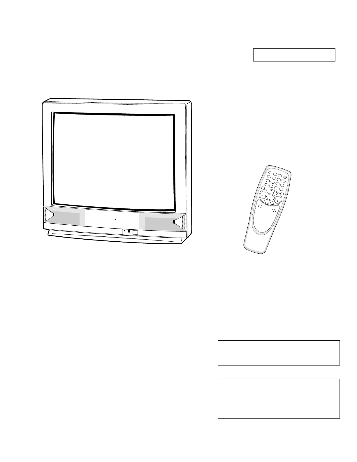
SERVICE MANUAL Colour Television
Product Code: 111355032
Original Ver sion
Chassis Series: LA5-A
C4CPS
FILE NO.
Model No. 29TC665
Service Ref. No.29TC665-00
(Argentina)
Give complete “SERVICE REF. NO.” for parts
order or servicing. It is shown on the rating
plate at the cabinet back of the unit.
This T.V. receiver will not work properly in
foreign countries where the television transmission system and power source differ from
the design specifications.Refer to the specification table.
Specifications
Power Source . . . . . . . . .AC220V, 50Hz / 60Hz
Receiving System . . . . . .PAL (M/M, N/N), NTSC (M/M)
Channel Coverage
Antenna mode VHF:CH02-CH13, UHF: CH14-CH69
CATV mode VHF band:CH01-CH13, Mid band: CH14-CH22
Super band: CH23-CH36, Hyper band: CH37-CH64
Ultra band: CH65-CH94 and CH100-CH125
Low mid band: CH95-CH99
Video IF . . . . . . . . . . . . . 45.75MHz
Aerial Input Impedance . . 75Ω
Ext.Terminals
Video inputs: Phono jack ✕ 2 (1Vp - p, 75Ω)
Audio inputs: Phono jack (R/L) ✕ 2 (436mVr ms, more than 40KΩ)
Headphone Jack: Mini stereo jack ✕ 1
Sound Output (RMS) . . . . 3W + 3W
Speakers . . . . . . . . . . . 5 cm x 9 cm x 2 pcs.
Dimensions . . . . . . . . . 656 (W) ✕ 600 (H) ✕ 496 (D)mm
Weight . . . . . . . . . . . . . approx.31.0 Kg
Specifications subject to change without notice.
1AV0U10B22200
JXMMA
POWER
A
U
D
IO
M
O
D
E
V
ID
E
O
M
O
D
E
5
9
6
3
0
2
8
7
4
1
SURROUND
MENU
VOL
VOL
CH
CH
NOBLEX
IMAGE
DISPLAY
MUTE
SLEEP
REC
ALL
SOUND
NOBLEX
NOBLEX
NOBLEX

Contents
-2-
Safety Notice . . . . . . . . . . . . . . . . . . . . . . . . . . . . . . . . . . . . . . . . . . . . . . . . . . . . . . . . . . . . . . . . . . . . . . . . 2
Chassis Block Diagram . . . . . . . . . . . . . . . . . . . . . . . . . . . . . . . . . . . . . . . . . . . . . . . . . . . . . . . . . . . . . . 3-4
IC Block Diagrams . . . . . . . . . . . . . . . . . . . . . . . . . . . . . . . . . . . . . . . . . . . . . . . . . . . . . . . . . . . . . . . . . . 5-7
Service Adjustments . . . . . . . . . . . . . . . . . . . . . . . . . . . . . . . . . . . . . . . . . . . . . . . . . . . . . . . . . . . . . . . . 8-16
Purity and Convergence Adjustment . . . . . . . . . . . . . . . . . . . . . . . . . . . . . . . . . . . . . . . . . . . . . . . . . . . . . 17
Cabinet Parts List . . . . . . . . . . . . . . . . . . . . . . . . . . . . . . . . . . . . . . . . . . . . . . . . . . . . . . . . . . . . . . . . . . . 18
Chassis Electrical Parts List . . . . . . . . . . . . . . . . . . . . . . . . . . . . . . . . . . . . . . . . . . . . . . . . . . . . . . . . . 19-27
Safety Notice
SAFETY PRECAUTIONS
1: An isolation transformer should be connected in the
power line between the receiver and the AC line
when a service is performed on the primar y of the
converter transformer of the set.
2: Comply with all caution and safety-related notes pro-
vided on the cabinet back, inside the cabinet, on the
chassis or the picture tube.
3: When replacing a chassis in the cabinet, always be
certain that all the protective devices are installed
properly, such as, control knobs, adjustment covers
or shields, barriers, isolation resistor-capacitor networks etc.. Before returning any television to the
customer, the service technician must be sure that
it is completely safe to operate without danger of
electrical shock.
X-RADIATION PRECAUTION
The primary source of X-RADIATION in television receiver is the picture tube.The picture tube is specially constructed to limit X-RADIATION emissions.For continued X-RADIATION protection, the replacement tube must be
the same type as the original including suffix letter.Excessive high voltage may produce potentially hazardous X
- RADIATION. To avoid such hazards , the high voltage must be maintained within specified limit.Refer to this service manual, high voltage adjustment for specific high voltage limit. If high voltage exceeds specified limits, take
necessary corrective action.Carefully follow the instructions for + B1 v olt po w er supply adjustment, and high voltage check to maintain the high voltage within the specified limits.
PRODUCT SAFETY NOTICE
Product safety should be considered when a component replacement is made in any area of a receiver.
Components indicated by mark in the parts list and the schematic diagram designate components in which
safety can be of special significance. It is par ticularly recommended that only par ts designated on the parts list
in this manual be used for component replacement designated by mark . No deviations from resistance
wattage or voltage ratings may be made for replacement items designated by mark .
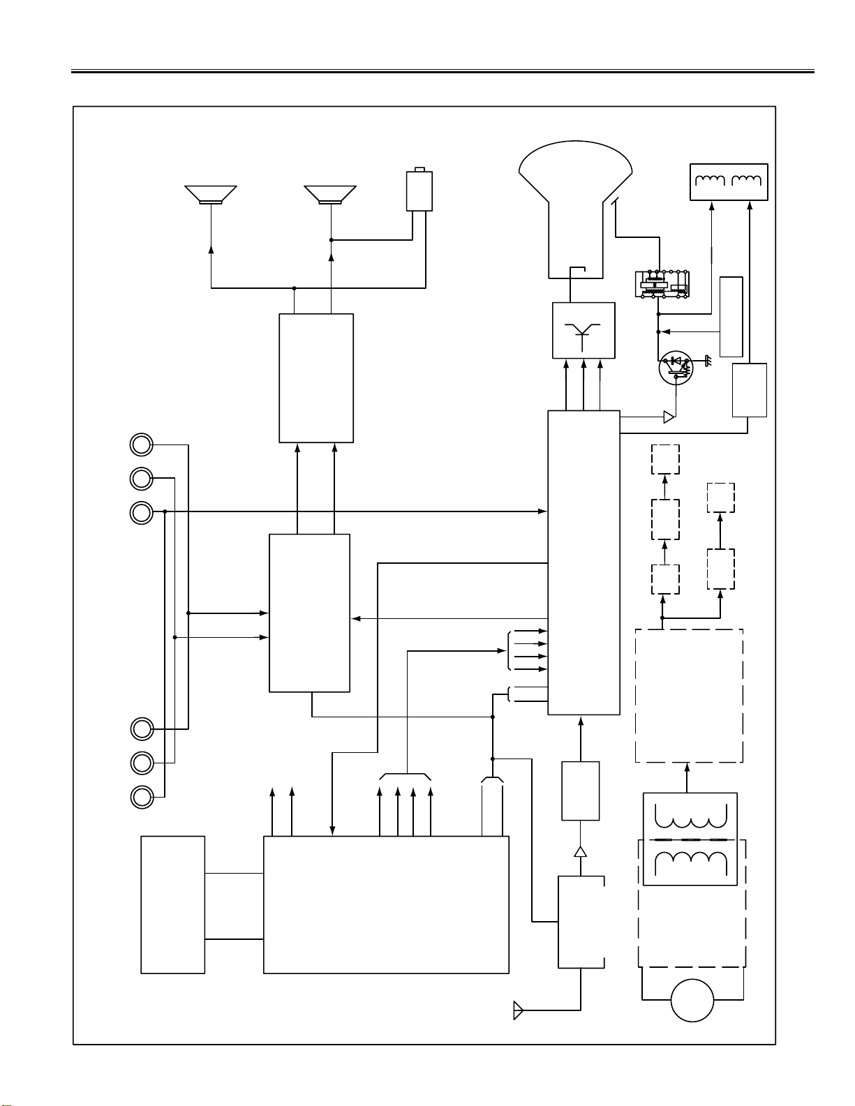
Chassis Block Diagrams
-3-
MAIN SIGNAL PROCESSING CIRCUIT
T611B
Q432
IC501
VERT-OUT
T471
HV
IC802
IC801
CPU
QXXAVC479P
5
6
3
4
TUNER
SAW
IC201
LA76818A
IC3401
CXA2134QP
IC002
LA42052-E
AUDIO AMP.
SDA
SCL
ON-TIMER
STANDBY
RGB
BLK
OSD
32
31
19
20
21
22
SDA
SCL
1
2
X161
A101
ANT
IF IN
5/6
SCL
SDA
R
G
B
BLK
12
11
14 15
16 17
13
34 33
3
4
4
2
42
FM OUTPUT
EXT VIDEO IN
K1001
K1002
REAR AV IN
FRONT AV IN
VIDEO
VIDEO
A-L
A-L
A-R
A-R
19
20
21
R
G
B
K1921
12
8
AC
POWER
CIRCUIT
CONVERTER
TRANS
130V(MAIN HIGH)
20V(AUDIO)
12V(MAIN LOW)
24V(VERT)
9V
IC202
REG.IC
5V-2
REG.IC
IC681
5VRC
2723
HORIZ-OUT
FBT
VERT.OUT
HORIZ.OUT
AUDIO RIGHT
AUDIO LEFT
HEADPHONE JACK
Q901
CRT
MEMORY
5/6
MTS DECODER/AUDIO CONTROL&SW
IIC BUS CONTROL
(WITH PLL)
FILTER
IF/VIDEO/CHROMA/DEFLECTION
DEFLECTION YOKE
2
R
L
15
C-CAPTION IN
40
SELECTED VIDEO OUT
EXT. L-IN
EXT. R-IN
SP901
SP902
PINCUSHION CIRCUIT
(Q461, Q462)
Chassis Block Diagrams
-4-
SYSTEM CONTROL
IC802
IC801
CPU
QXXAVC479P
5
6
3
4
SDA
SCL
32
31
19
20
21
22
1
2
MEMORY
15
17
27
6
18
10
12
13
29
23
28
7
CPU OSC IN
OSC
CPU OSC OUT
SOUND MUTE OUT
(ACTIVE=HIGH)
IC002
AUDIO AMP.
RESET IN (RESET=LOW)
KEY
SWITCH
KEY SWITCH IN
RC PRE-AMP
RC SIGNAL IN
RELAY ON/OFF OUT FOR DEGAUSSING
(ON=HIGH)
LED
ON-TIMER LED OUT
(ON=LOW)
IC3401
MTS
POWER ON/OFF OUT
(GREEN)
LED
(RED)
POWER CIRCUIT
SDA
SCL
A101
TUNER
IC201
IF/VIDEO/CHROMA
DEFLECTION
CIRCUIT
POWER CIRCUIT
etc.
AFT S-CURVE IN
C-CAPTION IN
OSD BLK OUT
OSD RED OUT
OSD GREEN OUT
OSD BLUE OUT
HORIZ. SYNC. IN
VERT. SYNC. IN
POWER PROTECT IN
(POWER ERROR=LOW)
(STANDBY=LOW)
IC Block Diagrams
-5-
IC201 < IF/Video/Chroma/Def. > LA76818A
1
DC
VOL
SW
FM
DET
2
3
4
56
IF
AGC
RF
AGC
VIF
7
8
9
10
IF
VCC 5V
11
12
13
BUS
PEAKING
CORING
BLACK
STRETCH
SYNC
SEP
14
15
ABL
DC
REST
CLAMP
OSD
CONTRAST
BRIGHT
16
17
18
19 20
CONTRAST
BRIGHT
RGB
MATRIX
OSD
SW
DRIVE/OUT-OFF
VCC
21
22
23
FSC/
SYNC SW
24
25
26 27
VER
RAMP
HOR
VCC
H
VCC
VER
C/D
HOR
OUT
PHASE
SHIFTER
AFC2
AFC1
VER
SEP
HOR
C/D
1/256
COLOR
CLAMP
LPF
ALC
+
SW
CLAMP
DEMO
PAL
SW
ACC
BPF
ON/OFF
DELAY
LINE
SW
TRAP
AFT
VIDEO
DET
TRAP
LIM
AMP
BPF
SPLL
BPF
VIDEO
AMP
IF
IDENT
VIDEO
SW
APC1
TINT
VXO
DDS
APC2
DC ADS.
CLAMP
VCO
1H DELAY
HOR
VCO
FBP
2829
30
31
32
1H
VCC
33
34
353637
38
39
40
41
42
CLMP
43
4445
CLMP
V/C VCC
5V
46
47
48
4950
A2C
PLL
51
525354
Audio Output
FM Output/Selected
Audio Output
PIF AGC
RF AGC Output
PIF Input1
PIF Input 2
IF Ground
IF Vcc
FM Filter
AFT Output
Bus Data
Bus Clock
ABL
Red Input
Green Input
Blue Input
Fast Blanking Input
RGB Vcc
Red Output
Green Output
Blue Output
fsc output or C
Sync output
Vertical Output
Ramp ALC Filter
Horizontal/BUS Vcc
Horizontal Output
Horizontal AFC Filter
Flyback Pulse Input
VCO IREF
Clock (4MHz) Outupt
CCD Vcc
CCD Filter
CCD/Horizontal Ground
SECAM B-Y Input
(Cb Input)
SECAM R-Y Input
(Cr Input)
Chroma APC2 Filter
Clamp Filter
4.43 MHz Crystal
Chroma APC1 Filter
Selected Video Output
Video/Vertical/BUS Ground
External Video Input(Y-IN)
Video/Vertical Vcc
Internal Video Input (S-C IN)
Black Level Detector
Video Output
VCO Filter
VCO Coil 2
VCO Coil 1
APC Filter
Ext. Audio Input
SIF Output
SIF APC Filter
SIF Input

IC Block Diagrams
-6-
IC201 <IF System Block Diagram> LA76818A
11
12
BUS
Interface
SAW
5
6
4
8
7
PIF
In1
PIF
In2
IF In
9V
30K
RF AGC
Out
120K
IF VCC
IF
GND
VIF AMP
VIF 1
VIF 2
VIF 3
IF AGC
Drive
RF
AGC
2ndIF
AGC
RF AGC
Delay
6bit
IF AGC
Def
1bit
+
-
(6 Vcc)/7
To
BUS
3
0.022u
PIF
AGC
IF
AGC
Data
Clock
APC
Det
+π/4
-π/4
Snd
Det
Amp
52
SIF.Out
Sound
Trap
Video
Det
Buzz
Canceller
50
APC
Filter
330
0.47u
+
PLL Pull-in SW
To
BUS
Lock
Det
Video.Level
3bit
Amp
54
10p
SIF.In
Sound
BPF
VCO.Coil
VCO
COIL1
VCO
COIL2
48
49
VIF
VCO
Chroma
Counter
B/N
INV
IF
Ident
OSC
C/D
Amp
SIF. Sys
2bit
pre-
scaller
SIF
VCO
500K
BPF
SIF
APC
Filter
1K
0.01u
1000p
53
LIM
AMP
FM
Det
FM.Level
5bit
Chroma
C/D
APC
Det
500K
Det
To
BUS
Chroma
VCO
VIF
Counter
Reset
Pulse
VCO
Ident
VIF.Sys
2bit
Phase
Detector
A.MUTE
1bit
VOLUME
D/A
VOLUME
Filter
A.SW
1bit
Input
Select
VOLUME
(ATT)
-
+
-
+
2.5V
Amp
FM Gain
1bit
Deem-TC
1bit
De-
emph
FM Mute
1 bit
2
9
46
51
1
A.Fil.Def
1bit
VOLUME
7bit
47
VCO
Alignment
AFT
10
AFT
Vcc
100K
100K
0.1u
VCO
Filter
+
0.47u
Audio.out
+
Audio in
10u
Video
Out
FM
Filter
+
1u
FM
Out
0.01u
+
to BUS Line
+

IC Block Diagrams
-7-
IC002 < Audio AMP. > LA42052-E
Thermal
Protection
-
+
AMP
Pump
Up
1
INVERTING
INPUT
2
Vcc
3
PUMP UP
OUT
4
GND
5
Ver. OUTPUT
6
OUTPUT
ST A GE Vcc
7
NON INV.
INPUT
IC501 < Vertical Output > LA78041-E, STV9379A
10
11
LFLT
VCO
12
PCINT1
PCINT2
PLINT
13
VCA
LPF
FLT
19
COMPIN
Vcc
17
Analog Block GND
23NOISETC
18
SAPTC
14
15
VGR
IREF
IREF
7
6
5
I
2
C BUS I/F
Digital Block GND
SCL
SDA
SAPIND
NOISE
DET
SAPVCO
BPF
STIND
1/4
1/2
LPF
DeEm
LPF
LPF
DeEm
AMP
(+4dB)
LPF
SW
24
25
22
SAPOUT
SAPIN
STIN
26 27
28
VE
VEWGT
LPF
HPF
LOGIC
NRSW/FOMO/SAPC
VCA
21
9
SUBOUT
(L-R signal output)
MAIN OUT
(L+R signal output)
8
MATRIX
VE
VCA
RMSDET
RMSDET
29
30 32 31
1
VETC
VEOUT
VCAIN
VCAWGT
VCATC
TREBLE OUT-L
SPECTRAL
34
33
FEXT1
TVSW
EXT1/EXT2/M1
M2
SURR
SURROUND
BASS
BASS
TREB
BASS
TREBLE
TREB
VOL-L
VOL-L
VOL-R
48
VOLIN-L
4
LSOUT-L
3
LSOUT-R
VOL-R
VOLUME RIGHT
CHANNEL INPUT
43
44
TREBLE OUT-R
41
47
TREBLE FILTER-L
45
2
BASS FILTER-L
40
SURRTC
38
TVOUT-R
39
TVOUT-L
36
37
AUX2-L
(Left channel
external input)
FEXT2
INPUT PIN OF (L+R)
SIGNALFROM
MAIN OUT(PIN9)
(+6dB)
WIDEBAND
"STEREO"
"NOISE"
"SAP"
"PONRES"
ATT/ATTSW
BASS FILTER-R
(Stereo block
PLL loop filter
integrating
pin)
(Pilot cancel
circuit loop filter
intergrating pin)
(Audio multiplexing
signal input)
AUX2-R
(Right channel
external input)
TREBLE FILTER-R
AUX1-L(Left channel
external input)
AUX1-R(Right channel
external input)
(Band gap reference
output)
(Sap FM detector
output)
(Input of L-R signal
from SUBOUT)
(Input of SAP signal)
(Variable de-
emphasis
integrating pin)
(Variable de-emphasis
output pin)
IC3401 < MTS Decoder, Audio Control & Switch > CXA2134QP-T6
1
2
3
PRE
GND
4
6
7
8
IN2
10
AMP
5
POWER
GND
IN1
RIPPLE
FILTER
P.P
VCC
STANDBY
OUT2
12
OUT1
AMP
INPUT AMP. OUTPUT AMP.
THERMAL
PROTECTION
CIRCUIT
AMP AMP
AMP
REF AMP.
RIPPLE FILTER
BLOCK
POP NOISE PREVENTION
BLOCK
INPUT AMP. OUTPUT AMP.
MENU
VOL
VOL
CH
VIDEO MODE
MENU
VOL
VOL
CH
CH
IMAGE
-8-
Service Adjustments
VOLUME +
VOLUME
-
CHANNEL UP
CHANNEL DOWN
POWER
3
21
MENU
S1.00110000 S2.01111000
ADDRESS DATA
02 H-PHA 08
Item No.
Item
Data value
General
This set has an On-screen Service Menu system included in the CPU that allows remote operation for most of the
service adjustments.
2. Service Adjustments:
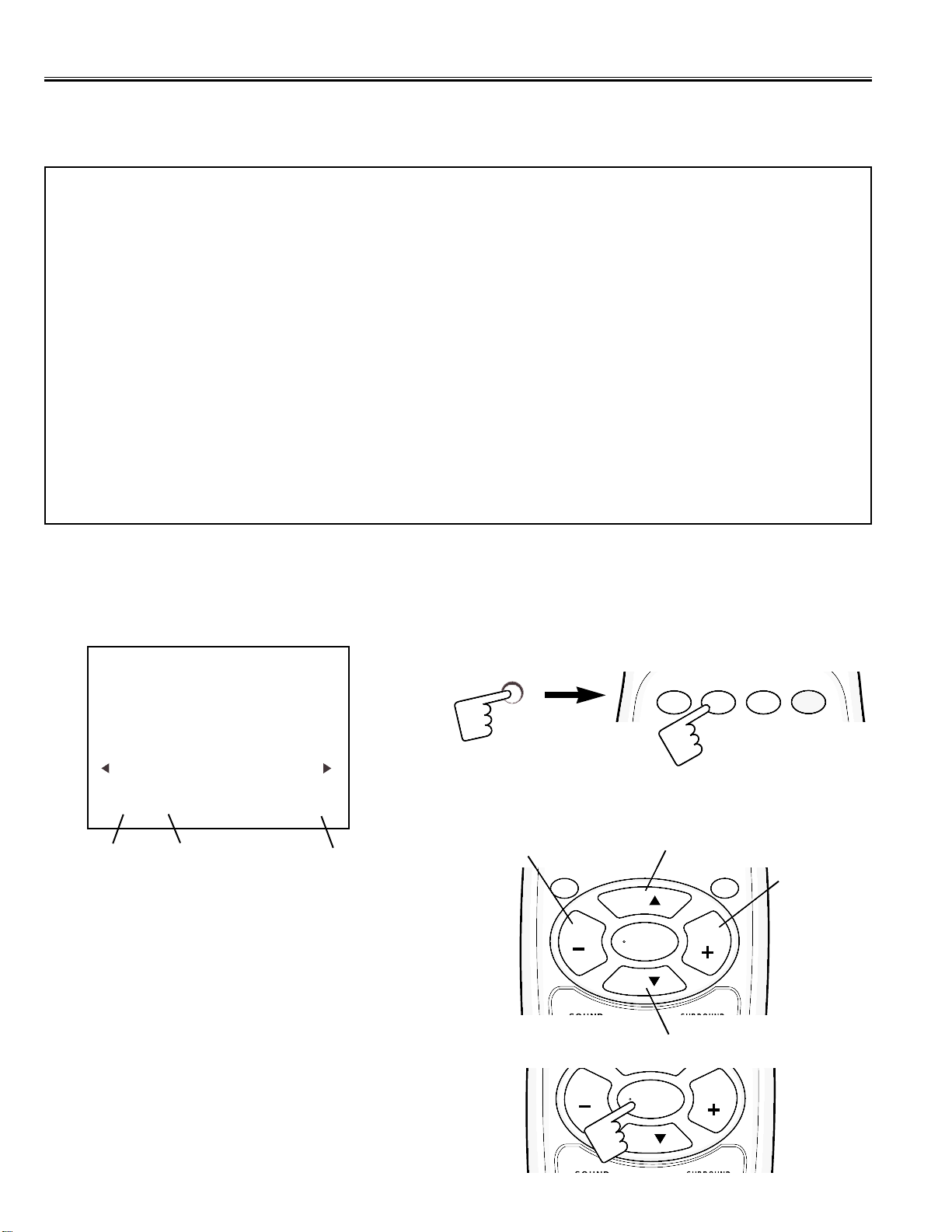
Press the CHANNEL UP or CHANNEL DOWN
button on the remote control handset to select the
desired service menu item you want to adjust.
Use the VOLUME + or-to adjust the data.The + or
-
button will increase or decrease the data
sequentially.
3. Exit from the Service Menu
Press the MENU button to turn off the Service Menu
display.
The data which is set in the service mode is stored
into the memory IC automatically.
[ Service Mode Display ]
Service Adjustment-1
1. Enter the Service Menu
While pressing the MENU button on the television, press the Number Key 2 on the remote control unit.
The Service Menu now appear.
IC802 (EEPROM) Replacement
When IC802 (EEPROM) is replaced, IC801 (CPU) will automatically write the initial reference data into IC802 for basic TV operation.
However, the bus data should be checked and some bus data should be set up before attempting the service adjustments. (See
pages 9 ~ 10 for detailed information.)
Initial Bus Data Setup
Note: When IC802 (EEPROM) is replaced, following Service Menu should be set up for proper TV operation before attempting the
service adjustments.
NO.01 RFAGC (Adjust the data 06 to10) NO.82 CHMT (Adjust the data 12 to 05) NO.308 R08 (Adjust the data FF to 21)
NO.05 V-SCO (Adjust the data 17 to 11) NO.84 RELAY (Adjust the data 80 to 20) NO.309 R09 (Adjust the data FF to 95)
NO.06 V-LIN (Adjust the data 15 to 16) NO.85 CCD (Adjust the data 26 to 31) NO.310 R10 (Adjust the data FF to 50)
NO.11 VLI60 (Adjust the data +1 to 0) NO.300 R00 (Adjust the data FF to 93) NO.311 R11 (Adjust the data FF to 00)
NO.19 RDRIV (Adjust the data 63 to 64) NO.301 R01 (Adjust the data FF to 0E) ↓↓
NO.20 GDRIV (Adjust the data 07 to 08) NO.302 R02 (Adjust the data FF to 00) NO.371 R71 (Adjust the data FF to 00)
NO.21 BDRIV (Adjust the data 63 to 64) NO.303 R03 (Adjust the data FF to 00) NO.372 R72 (Adjust the data FF to A2)
NO.24 B-YD (Adjust the data 10 to 08) NO.304 R04 (Adjust the data FF to 01)
NO.25 R-YD (Adjust the data 10 to 08) NO.305 R05 (Adjust the data FF to 00)
NO.68 AFCAV (Adjust the data 00 to 01) NO.306 R06 (Adjust the data FF to 00)
NO.81 POMT (Adjust the data 12 to 08) NO.307 R07 (Adjust the data FF to 00)

-9-
Service Adjustments
No. Item Initial value Range Description
01 RFAGC 06→10* 00~63 RF AGC adjustment
02 H-PHA 08 00~31 H-PHASE adjustment (50Hz)
03 V-POS 32 00~63 Vertical position adjustment (50Hz)
04 V-SIZ 54 00~127 Vertical size adjustment (50Hz)
05 V-SCO 17→11* 00~31 Vertical-S compensation (50Hz)
06 VLIN 15→16* 00~31 Vertical linearity adjustment (50Hz)
07 H-P60 +4 -16~+15 Difference value of H-PHASE adjustment (60Hz)
08 V-P60 0 -32~+31 Difference value of V-POSITION adjustment (60Hz)
09 V-S60 +1 -64~+63 Difference value of V-SIZE adjustment (60Hz)
10 VSC60 0 -16~+15 Difference value of Vertical-S compensation (60Hz)
11 VLI60 +1→0* -16~+15 Difference value of Vertical linearity adjustment (60Hz)
12 OSDHP 30 01~255 OSD horizontal remark position
13 OSDC 50 00~127 OSD contrast
14 V-SCP 07 00~07 V-SIZE COMP (50Hz)
15 SBIAS 70 00~127 Sub Bias adjustment
16 RBIAS 00 00~255 Red Bias adjustment
17 GBIAS 00 00~255 Green Bias adjustment
18 BBIAS 00 00~255 Blue Bias adjustment
19 RDRIV 63→64* 00~127 Red Dr ive adjustment
20 GDRIV 07→08* 00~15 Green Drive adjustment
21 BDRIV 63→64* 00~127 Blue Drive adjustment
22
-- -- --
White balance (a lateral line)
23 DRV
-- --
Brightness and dark of White balance adjustment
24 B-YD 10→08* 00~15 B-Y DC Level
25 R-YD 10→08* 00~15 R-Y DC Level
26 B-YND 0 -16~+15 Difference value of NTSC B-Y DC Level
27 R-YND 0 -16~+15 Difference value of NTSC R-Y DC Level
28 G-YA 00 00,01 G-Y Angle
29 RBGB 08 00~15 R-Y/B-Y Gain Balance
30 RBAG 08 00~15 R-Y/B-Y Angle
31 G-YAN 00 00,01 Difference value of NTSC G-Y Angle
32 RBGBN 0 -8~+7 Difference value of NTSC R-Y/B-Y Gain Balance
33 RBABN 0 -8~+7 Difference value of NTSC R-Y/B-Y Angle
34 COGV 01 00~03 Cor ing gain
35 BLK 03 00~03 BLK. STR. Star t (W/Defeat)
36 BLKG 03 00~03 BLK. STR. Gain
37 BRTA 00 00, 01 BRT. ABL Defeat
38 BRST 00 00, 01 Mid. Stp. Defeat
39 BRTH 00 00~07 Bright. ABL.Threshold
40 WPL 00 00~03 WPL Ope. Point (W/Defeat)
41 YGAM 00 00~03 Y Gamma Start
42 PORW 00 00, 01 AV Mode Pre/Over SW
43 PORS 02 00~03 AV Mode Pre/Over-shoot adjustment
44 RFCO 0 00~03 Difference Value of RF Corring Gain
45 PORWN 01 00, 01 RF Pre/Over SW
46 PORSN 03 00~03 RF Pre/Over-shoot adjustment
47 TINT 0 -16~+15 Tint
48 SHRF 0 -16~+15 Difference Value of RF Sharpness
49 TEXC 08 00~127 OSD Text Contrast
50 AUFL 00 00, 01 Auto.Fresh
On-screen Service Menu
Following table shows the initial values which have been stored in the CPU ROM, and items for the service adjustments.
When IC802 (EEPROM) is replaced, check the bus data to confirm they are the same as below.The shaded menu should be checked
and be set up or readjusted according to the procedures described in the following pages.
Initial Setup Data marked with an * should be changed from Initial Value Data.
 Loading...