

NOBLEX 24 LC827H Schematic
Model No. 24LC827H
Service Ref.No. 24LC827H-00
SERVICE MANUAL LCD Television
Product Code: 1-130-259-18
Original Version
Chassis Series: UE7-M
Z5JY
Contents
FILE NO.
Give complete "SERVICE REF. NO." for
parts order or servicing.It is shown on the
rating lable at the cabinet back of the unit.
This T.V. receiver will not work properly
in foreign countries where the television
transmission system and power source
differ from the design speci cations. Refer
to the speci cation table.
REFERENCE NO.
Safety Notice............................................... 2
Speci cations.............................................. 3
Chassis Block Diagrams.......................... 4-5
IC Block Diagrams ................................. 6-10
On-screen Service Menu System......... 11-15
Service Adjustments.................................. 16
Mechanical Disassembly...................... 17-20
Cabinet Parts List...................................... 21
Chassis Electrical Parts List................. 22-31
Printed Wiring Board............................ 32-36
Schematic Diagram.............................. 37-39
(Argentina)
NOBLEX
Safety Notice
Safety Precautions
The following precautions must be observed.
1:Comply with all caution and safety-related notes provided on the cabinet back, cabinet bottom, inside the
cabinet or on the chassis.
2:When replacing a chassis in the cabinet, always be certain that all the protective devices are installed
properly, such as, control knobs, adjustment covers or shields, barriers, etc..
DO NOT OPERATE THIS TELEVISION WITHOUT THE PROTECTIVE SHIELD IN POSITION AND
PROPERLY SECURED
3:Before replacing the cabinet cover, thoroughly inspect the inside of the cabinet to see that no stray parts or
tools have been left inside.
Before returning any televison to the customer, the service personnel must be sure that it is completely safe
to operate without danger of electrical shock.
Product Safety Notice
Product safety should be considered when a component replacement is made in any area of a receiver.
Components indicated by mark in the parts list and the schematic diagram designate components in
which safety can be of special signicance.
It is particularly recommended that only parts designated on the parts list in this manual be used for
component replacement designated by mark .
No deviations from resistance wattage or voltage ratings may be made for replacement items designated
by mark .
-2-

Specications
Power Source AC 110 - 240 Volts, 50/60 Hz
Receiving System PAL-N, PAL-M, NTSC3.58
Channel Coverage ANTENNA mode
VHF: CH02 - CH13
UHF: CH14 - CH69
CATV mode
VHF band: CH01-CH13
MID band: CH14-CH22
SUPER band: CH23-CH36
HYPER band: CH37-CH64
ULTRA band: CH65-CH94 and CH100-CH125
Low MID band: CH95-CH99
Aerial Input Impedance 75 Ω
LCD panel Screen Size (Measured Diagonally): 24 inches
Picture Resolution: WXGA 1366 (Horiz..) x 768 (Vert.) pixels
Brightness: 320 cd/m2
Audio Output (RMS) 3 W + 3 W
Speaker Size Mains: 32.5mm x 87.0mm x 2pcs
Input and Output terminals
AV1 Input Video Input: Composite video Input (RCA Jack) x1
Audio Input: L/R Stereo Input (RCA Jack) x 1 set
AV2 Input Video Input: Component Y (combined with composite video input),
CB, CR Input (RCA Jack) x1 set
Audio: L/R Stereo Input (RCA Jack) x 1 set
HDMI Input HDMI Terminal 19 pin x1
PC Input Video Input: D-SUB 15 pin x1
Audio Input: Mini stereo jack x 1
Output Terminals Video Monitor Output: RCA jack x 1
Audio Monitor Output: L/R Stereo Output (RCA jack) x 1 set
Headphone Jack: Mini stereo jack x1
Dimensions
(Width x Height x Depth) 607.8 x 425.1 x 189.8 mm (Including Stand)
Net Weight
(Including Stand ) 5.4 KG
Environmental Considerations
Operating Temperature 0˚C ~ 40˚C (32˚F ~ 104˚F)
Operating Humidity 20 ~ 80%
Storage Temperature -10˚C ~ 50˚C (14˚F ~ 122˚F)
Storage Humidity 20 ~ 80 %
Accessories Owner’s Manual
Remote Control
Place of Production Argentina
-3-
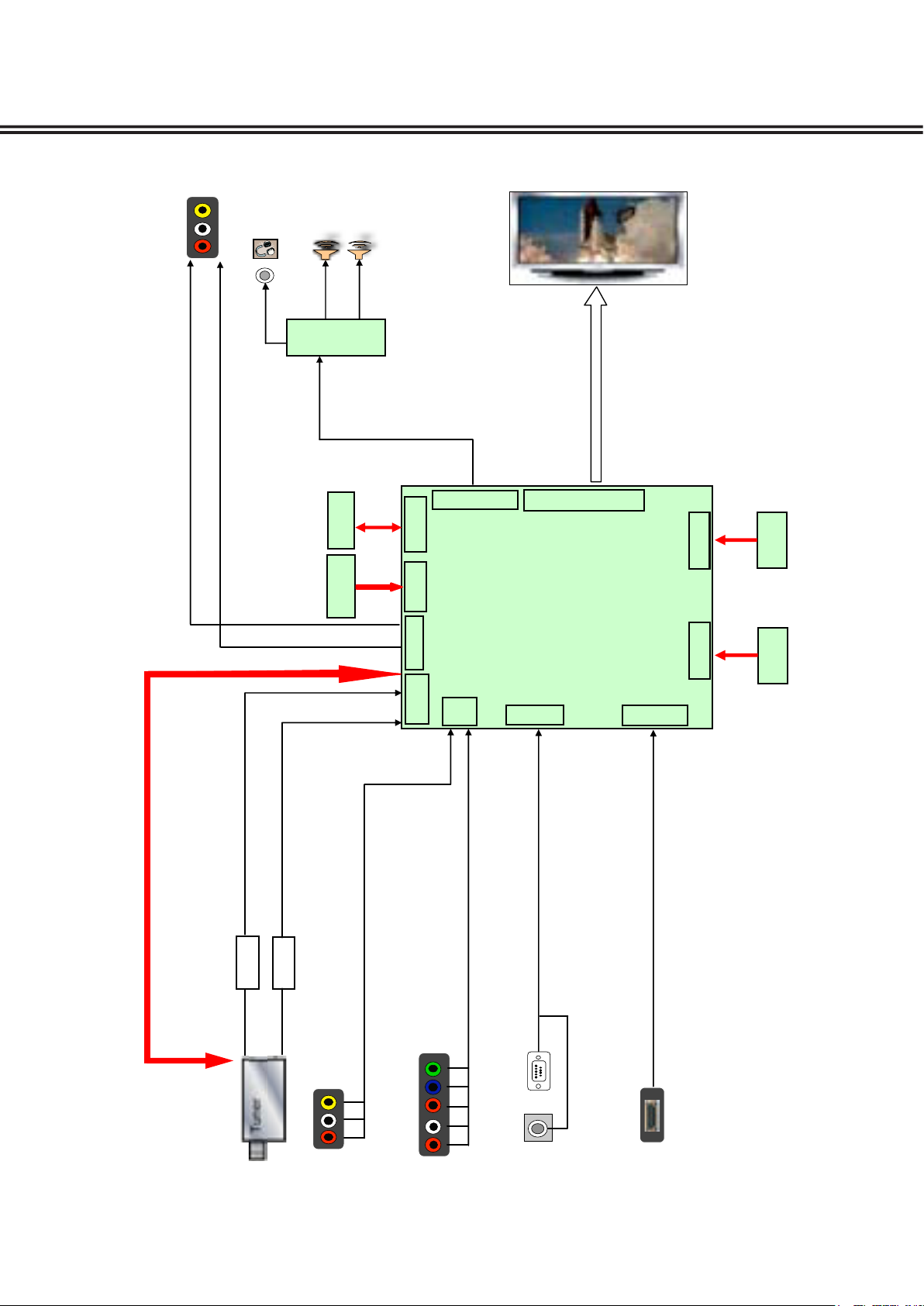
Chassis Block Diagrams
IC7200
MST740KU
A101
R L V
VGA
HDMI
R L V
Video in
L/R in
R/G/B in
L/R OUT
SPI FLASH
24LA64AT
FFC
I2C
TPA1517DWPR
AV2/DVD
L/R in
L/R in
audio out
video out
D3502H
HDM
I
VGA
AV1
AV2
SIF VIF
Monitor
FLASH
LVDSOUT
AUDIO
RC
KEY
RC
KEY
PC
PANEL
Tuner
Tuner
AV1
R L PR PB Y
Monitor out
L/R Speaker
MAIN SIGNAL PROCESSING CIRCUIT
-4-
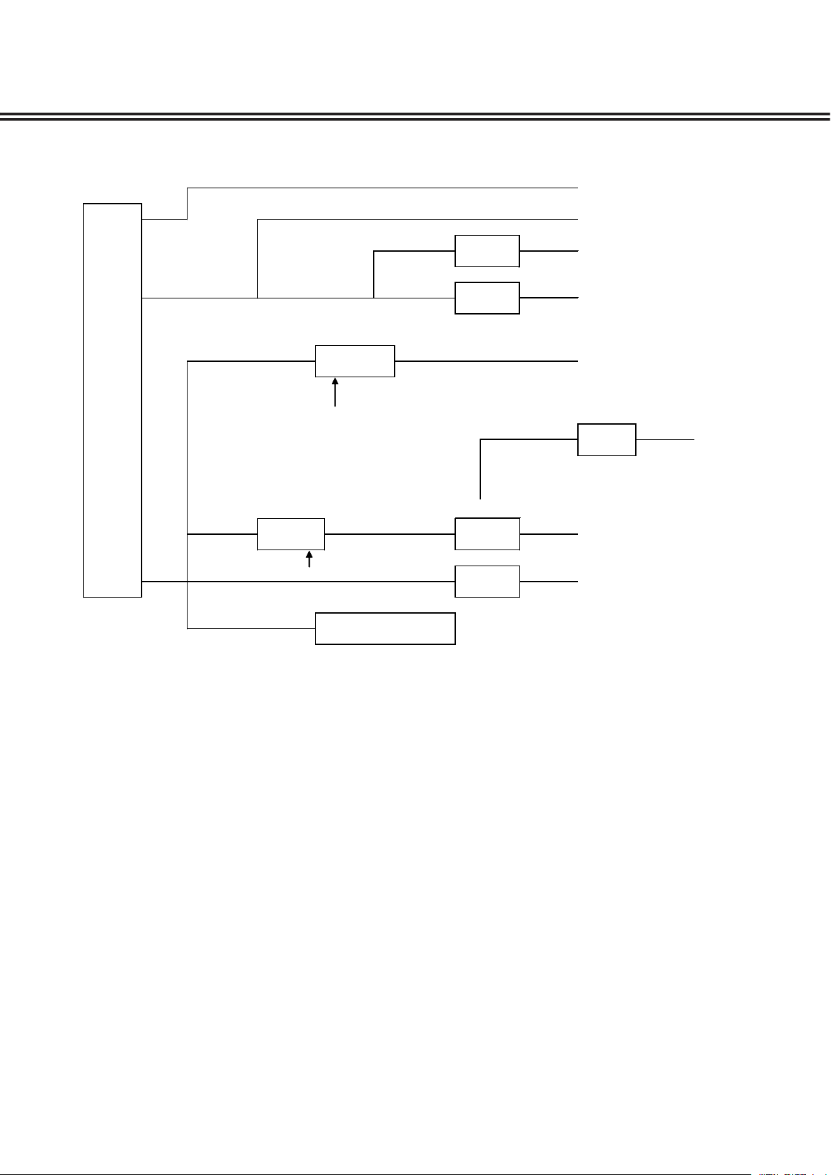
POWER SUPPLY IC
1.3A
13V (1.3A) 100mA
100mA
(0.3A)
100mA
900mA
ON-PANEL (MAIN)
600mA
3.3V_2
5VD
600mA
PWR-ON
5VSTB
(2.3A)
50mA
100mA
1.26VA
+5VSTB
LDO
3.3VSTB
CMOS SW
5VP FOR PANEL
IR/LED/EEPROM
CMOS SW
LDO
12V FOR AUDIO AMP
FOR MONITOR OUT
DC/DC
33V FOR TUNER
+13VA
+12V
AVDD_AU & AVDD_VIF
& 3.3VD & AVDDA & VDDP
LDO
LDO
5VT FOR TUNER
Chassis Block Diagrams
-5-
IC Block Diagrams (On the ASSY, PWB, MAIN)
FLK3
VGH_EVEN
OPT_P1
GCLK1
VGH_ODD
GCLK2
OPT_N1
GCLK3
SOE
HCONV1
SC_FS
AUVRADP
AUVREF
RXE4-
CVBS1
SV_Y0
CVBS0
SV_C0
CVBSOut1
VCOM0
B_TX0+
B_TX0-
R_TX2-
G_TX1G_TX1+
TXCLK-
R_TX2+
RXO1+RLV1N
PB+
TXD
TAGC
FLK1
SPI_CZ
SPI_CK
SPI_DO1
SPI_DI
AUOutL2
RXE4+
SAR0
SAR1
SIFP
SIFM
PWM0
RXO2-RLV2P
PWM2
VIFM
VIFP
LED_R
LED_Y
RXE1-RLV7P
FLK2
SIF-CTL
AUOutR2
HDCEC
RXO2+RLV2N
RXE1+RLV7N
TXCLK+
RXOC-
AUVRADN
LEDON1
SCAN_BLK2
RXE2-
WPWM1
HWRESET
SOG
BIN+
RIN+
GIN+
SCL_HD
SDA_HD
HPLUG
RXOC+
WAKEUP
RXE2+
SCAN_BLK1
RXO3-RLV4P
PWM1
RXEC-
I2C_SCL
I2C_SDA
DPM1
RXO3+RLV4N
IR_SYNC
SOY
PR+
Y+
RXEC+
RXO0-RLV0P
RXO4-RLV5P
RXE3-
AMP-MUTE
AUOutR1_amp
AUOutL1_amp
RXO0+RLV0N
ON-PANEL
ON-PBACK
COMP_AUL2
PC_AUR0
AV_AUL1
AV_AUR1
PC_AUL0
COMP_AUR2
RXO4+RLV5N
RXE3+
RXO1-RLV1P
RXD
HS_RGB
VS_RGB
HD-SW
SC_FB
GCLK4
PWM3
GCLK5
POL
GCLK6
WP_EE
GSP
RXE0+RLV6N
RXE0-RLV6P
AVDDA
VDDP
VDDC
AVDD_AU
AVDD_VIF
+5V_all
VDDP_PM
AVDD_MPLL
VGH_EVEN
RXOC+
RXOC-
RXO3+
RXO3-
RXO4-
RXO0+
RXO0-
RXO1+
RXO1-
RXO2+
RXO2-
PWM3
GCLK6
GCLK5
RXO4+
GCLK4
POL
RXE0-
RXE1+
RXE1-
RXE2+
RXE2-
RXEC+
RXEC-
RXE3+
RXE3-
RXE4+
RXE4-
RXE0+
GSP
GCLK1
GCLK2
GCLK3
SOE
ADJ_PWM
I2C_SDA
I2C_SCL
RXD
TXD
VGH_ODD
MST740KU
Please close
to chip.
CL=20pf of XTAL
WARNING !!!
PANEL
INTERFACE
C158
27pF
C158
27pF
R217 22RR217 22R
C169
0.1uF
C169
0.1uF
TP26TP26
TP14TP14
R183 100RR183 100R
R176 22RR176 22R
R239 NC/100RR239 NC/100R
TP15TP15
TP19TP19
R174
4.7K
R174
4.7K
TP17TP17
+
C164 10uF/16V
+
C164 10uF/16V
C159
27pF
C159
27pF
7 5 3 1
8 6 4 2
RP9
RP22X4
7 5 3 1
8 6 4 2
RP9
RP22X4
+
C175
10uF/16V
+
C175
10uF/16V
R241 22RR241 22R
R172 68RR172 68R
AVSS_ADC
3
AVDD_ADC
10
AVSS_ADC
25
AVDD_MPLL
26
SPI_SCK91SPI_SDI89SPI_SCZ90SPI_SDO
88
DDCA_DAT
126
INT
127
HWRESET
135
XTAL_XOUT
27
XTAL_XIN
28
DDCA_CLK
125
IRIN
128
AUWS/GPIO83GPIO/SPI_SIO386GPIO85AUMCKO/GPIO
84
AVDD_VIF
39
AVSS_MPLL
29
VSYNC1
9
AVDD_VIF
30
AUSCK/GPIO82AUSD0/GPIO
81
AVDD_ADC
18
GPIO/SPI_SIO2
87
GPIOD3/TXD194GPIOD2/RXD1
95
AVSS
52
MUTE/GPIOD592GPIOD4
93
GPIOD1/RXD096GPIOD0/TXD0
97
LVB4N
98
LVB4P
99
LVB3N
100
LVB3P
101
LVBCLKN
102
LVBCLKP
103
RLV8N/LVB2N
104
RLV8P/LVB2P
105
RLV6N/LVB0N
108
RLV6P/LVB0P
109
RLV5N/LVA4N
111
RLV5P/LVA4P
112
RLV4N/LVA3N
113
RLV4P/LVA3P
114
RLV3N/LVACLKN
115
RLV3P/LVACLKP
116
RLV2N/LVA2N
117
RLV2P/LVA2P
118
RLV1N/LVA1N
119
RLV1P/LVA1P
120
AVDDP_1
124
GND
68
AVDD_ADC
153
AVDD_VIF
31
RLV7P/LVB1P
107
RLV7N/LVB1N
106
RLV0P/LVA0P
122
RLV0N/LVA0N
121
TCON5
62
TCON6
63
TCON7
64
TCON8
65
TCON9
66
TCON10
70
TCON11
71
TCON12
72
GND
147
SAR0
131
SAR1
130
SAR2
129
WAKEUP
137
TCON0
57
TCON1
58
TCON2
59
TCON3
60
TCON4
61
TCON13
73
AVDDP_1
110
PWM276PWM177PWM0
78
GND
79
AVDDP_1
69
TCON14
145
TCON15
144
TCON16
143
TCON17
142
TCON18
141
TCON19
140
TCON20
139
TCON21
138
AVDDP_1
74
VDDC
67
AVDDP_1
80
VDDP_2
132
VDDC
148
AVSS_VIF32AVSS_VIF
37
AVDD_AU
41
GND
123
DDCD_SCL
133
RIN1P
8
RXA0P
152
LINE_IN_1R
45
BIN1P
4
HOTPLUG
156
RXACKP
150
LINE_IN_2L
46
SIFP
36
GIN1P
6
CVBS0/Y0
22
CVBS2/Y1
20
AUVRP
50
DDCD_SDA
134
BIN0P
12
CEC
136
LINE_IN_0R
43
DAC_OUT_L
53
HSYNC0
11
AUVAG
51
RIN0P
16
AUCOM
48
SOGIN0
15
SOGIN1
5
RXA2P
2
RXA1N
154
RXA2N
1
VCOM0
23
GIN0M
13
RXA0N
151
LINE_IN_1L
44
LINE_IN_2R
47
AUVRM
49
LINE_IN_0L
42
TAGC
40
RXACKN
149
GIN1M
7
SIFM
35
VIFM
34
CVBSOUT
24
CVBS1/C0
21
RXA1P
155
DAC_OUT_R
54
VSYNC0
17
VR27
38
VIFP
33
CVBS3/C1
19
GIN0P
14
LINE_OUT_L
55
LINE_OUT_R
56
AVDDP_1
146
PWM375EPAD
157
U18U18
C165 0.1uFC165 0.1uF
R238 22RR238 22R
R167 200RR167 200R
TP23TP23
TP16TP16
TP21TP21
TP27TP27
X1
14.318MHZX114.318MHZ
R208 22RR208 22R
C162 47nFC162 47nF
C161 47nFC161 47nF
R179 0RR179 0R
7 5 3 1
8 6 4 2
RP3
RP22X4
7 5 3 1
8 6 4 2
RP3
RP22X4
C168
0.1uF
C168
0.1uF
7 5 3 1
8 6 4 2
RP4
RP22X4
7 5 3 1
8 6 4 2
RP4
RP22X4
TP18TP18
C171 0.1uFC171 0.1uF
L20
120R/FB0603
L20
120R/FB0603
L21FBL21
FB
TP13TP13
R173 68RR173 68R
R244 22RR244 22R
C174
1uF
C174
1uF
7 5 3 1
8 6 4 2
RP5
RP22X4
7 5 3 1
8 6 4 2
RP5
RP22X4
R177 22RR177 22R
TP22TP22
R1661MR166
1M
R171 68RR171 68R
TP25TP25
R228 10K/NCR228 10K/NC
R181 0RR181 0R
7531
8642
RP7
RP22X4
7531
8642
RP7
RP22X4
C115 47nFC115 47nF
R180 0RR180 0R
C170
100pF
C170
100pF
R237 22RR237 22R
7 5 3 1
8 6 4 2
RP1
RP22X4
7 5 3 1
8 6 4 2
RP1
RP22X4
R227 22RR227 22R
C172
0.1uF
C172
0.1uF
R182 0RR182 0R
7 5 3 1
8 6 4 2
RP2
RP22X4
7 5 3 1
8 6 4 2
RP2
RP22X4
R214 22RR214 22R
TP24TP24
TP20TP20
C173
4.7uF
C173
4.7uF
R245 22RR245 22R
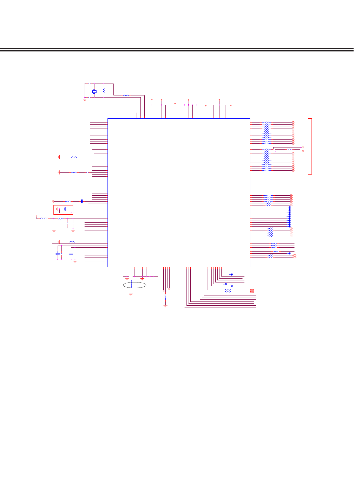
IC7200 MST740KU MST740KU
-6-
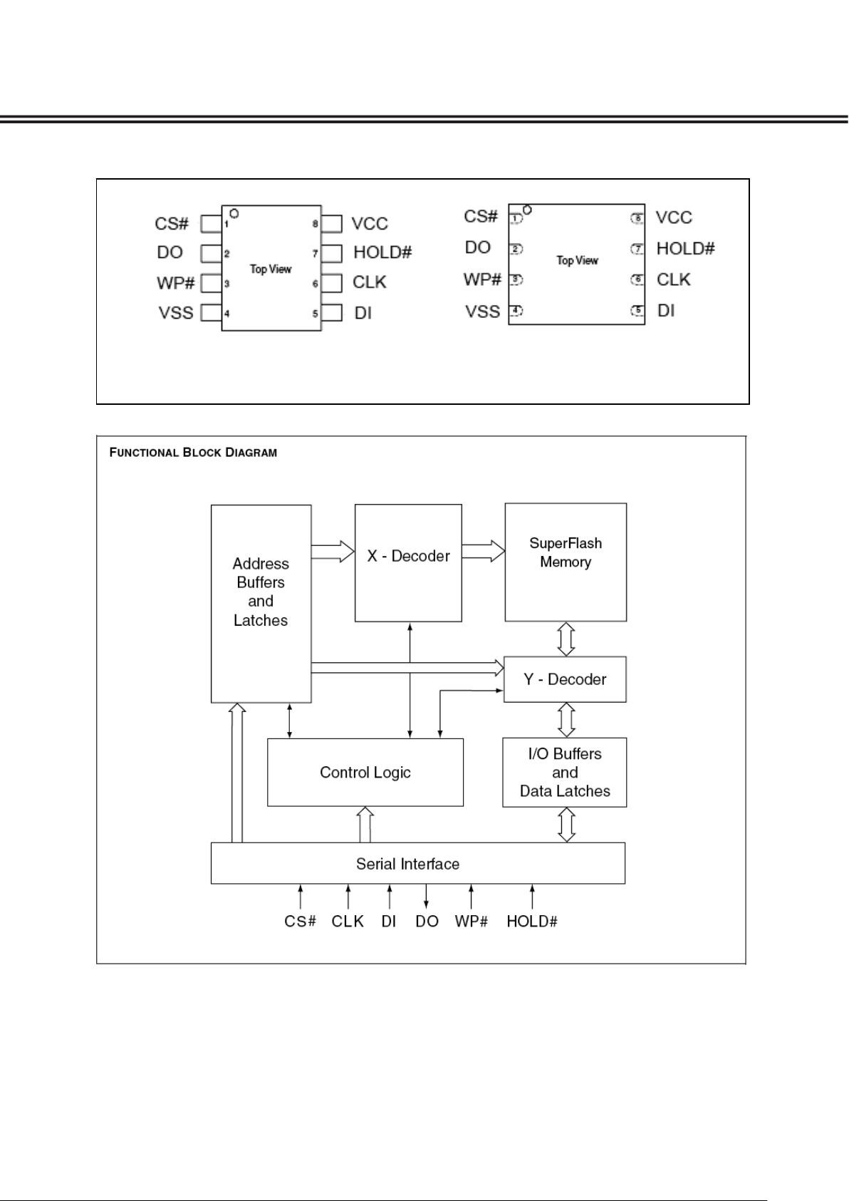
EN25F80
8 - LEAD SOP / PDIP 8 - CONTACT VDFN
IC8000 �XXAAJ�1352-- �XXAAJ�1352--
EN25F80
Figure.1 CONNECTION DIAGRAMS
ʳ
Figure 2. BLOCK DIAGRAM
8 - LEAD SOP / PDIP 8 - CONTACT VDFN
IC Block Diagrams
-7-
IC Block Diagrams
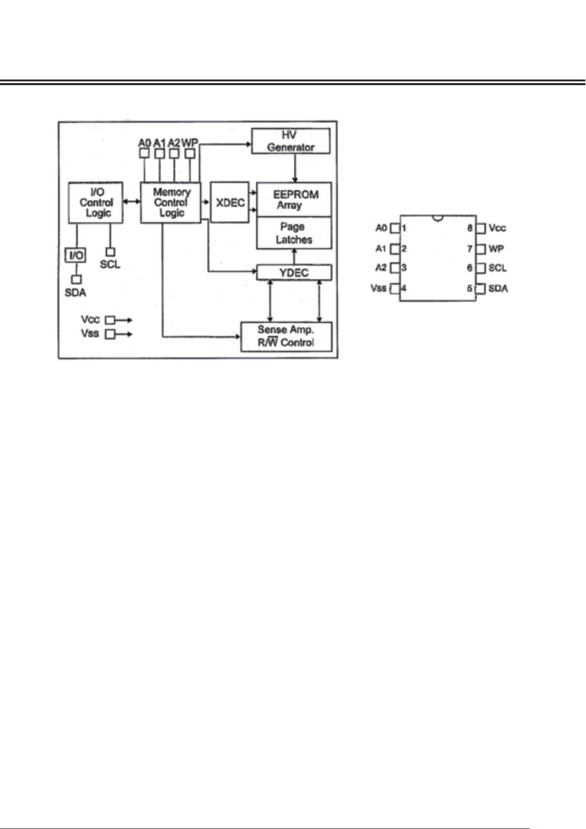
IC8001 �XXAVC951---P
-8-
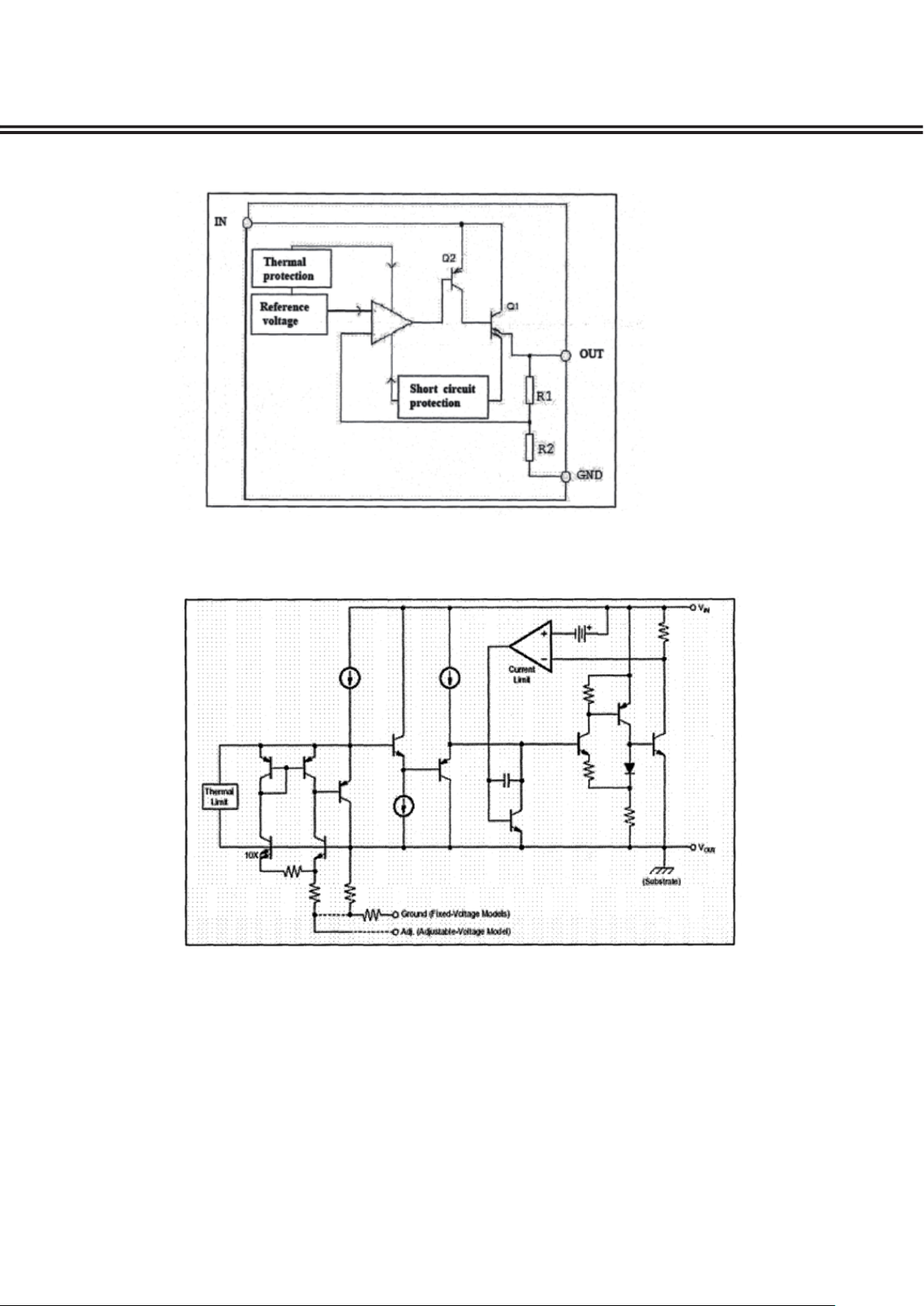
IC7502 �LM1085R-3.3P
IC Block Diagrams
IC7504 �LM1117S-ADJP
-9-
IC Block Diagrams
IC001 �TPA1517DWPRP
-10-
On-screen Service Menu System
General
This set has an On-screen Service Menu System included in the CPU that allows remote operation for
most of the service adjustments.
On-screen Service Menu System
�uick operation is needed to enter Service Mode.
■ How to enter the Service Menu
1. Press and hold the MENU button on Side Controls.
2. Keep pressing the MENU button and press the "MUTE" button on the remote control, and the FACTORY
MENU will be displayed.
3.
Select SERVICE by pressing ▲▼ button, and press ◄► button to enter.
Side Controls
MENU button
Open or close the
On-Screen Menu.
Remote Control
[ Service Mode Menu ]
SERVICE
INDEX-000 575i SUB- CONT
ADD 0B60
DATA FD 1 1 1 1 1 1 0 1
■ How to select the service item and adjust data:
To adjust data:
1) Select “DATA” line by pressing ▲▼ button.
SERVICE
INDEX-000 575i SUB- CONT
ADD 0B60
DATA FD 1 1 1 1 1 1 0 1
▲▼◄►
button
Item Name
Address
Data Value
2) Press ◄► button to adjust data.
■ To exit service mode
Press MENU button to exit service mode.
Note: The all adjusted data in service mode will be memorized into EEPROM automatically.
-11-

On-screen Service Menu System
■ Service Adjustment Data Table
Item Name Initial Data IC Description
575i SUB-CONT FD MST740KU
575i SUB-BRIGHT FF MST740KU DVD Input
575i SUB-COLOR 0B MST740KU Input Video Format: 575i
575i SUB-TINT 07 MST740KU (Different Value)
575i SUB-SHARP 00 MST740KU
575p SUB-CONT FD MST740KU
575p SUB-BRIGHT FF MST740KU DVD Input
575p SUB-COLOR 0B MST740KU Input Video Format: 575p
575p SUB-TINT 07 MST740KU (Different Value)
575p SUB-SHARP 00 MST740KU
480i SUB-CONT FD MST740KU
480i SUB-BRIGHT FF MST740KU DVD Input
480i SUB-COLOR 0B MST740KU Input Video Format: 480i
480i SUB-TINT 07 MST740KU (Different Value)
480i SUB-SHARP 00 MST740KU
480p SUB-CONT
480p SUB-BRIGHT FF MST740KU DVD Input
480p SUB-COLOR 0B MST740KU Input Video Format: 480p
480p SUB-TINT 07 MST740KU (Different Value)
480p SUB-SHARP 04 MST740KU
1080i(50) SUB-CONT FD MST740KU
1080i(50) SUB-BRIGHT FF MST740KU DVD Input
1080i(50) SUB-COLOR 0B MST740KU Input Video Format:1080i(50)
1080i(50) SUB-TINT 07 MST740KU (Different Value)
1080i(50) SUB-SHARP 00 MST740KU
1080i(60) SUB-CONT 01 MST740KU
1080i(60) SUB-BRIGHT FE MST740KU DVD Input
1080i(60) SUB-COLOR
1080i(60) SUB-TINT 07 MST740KU (Different Value)
1080i(60) SUB-SHARP 00 MST740KU
720p50 SUB-CONT FE MST740KU DVD Input
720p50 SUB-BRIGHT FE MST740KU Input Video Format: 720p(50)
720p50 SUB-COLOR 0B MST740KU (Different Value)
720p50 SUB-TINT 07 MST740KU
720p50 SUB-SHARP 00 MST740KU
720p60 SUB-CONT FD MST740KU DVD Input
720p60 SUB-BRIGHT FF MST740KU Input Video Format: 720p(60)
720p60 SUB-COLOR 0B MST740KU (Different Value)
720p60 SUB-TINT 07 MST740KU
720p60 SUB-SHARP 00 MST740KU
1080P(50) SUB-CONT FF MST740KU DVD Input
1080P(50) SUB-BRIGHT FF
1080P(50) SUB-COLOR 0B MST740KU (Different Value)
1080P(50) SUB-TINT 07 MST740KU
1080P(50) SUB-SHARP
1080P(60) SUB-CONT FF MST740KU DVD Input
1080P(60) SUB-BRIGHT FF MST740KU Input Video Format: 1080P(60)
1080P(60) SUB-COLOR 0B MST740KU (Different Value)
1080P(60) SUB-TINT 07 MST740KU
1080P(60) SUB-SHARP
PC SUB-CONT 08 MST740KU
PC SUB-BRIGHT 01 MST740KU
PC SUB-COLOR 00 MST740KU PC Input
PC SUB-TINT 00 MST740KU (Different Value)
FD MST740KU
0B MST740KU Input Video Format: 1080i(60)
MST740KU Input Video Format: 1080P(50)
00 MST740KU
00 MST740KU
-12-

On-screen Service Menu System
Item Name Initial Data IC Description
PC SUB-SHARP 00 MST740KU
DVI SUB-CONT 16 MST740KU
DVI SUB-BRIGHT FA MST740KU
DVI SUB-COLOR 00 MST740KU DVI Input
DVI SUB-TINT 04 MST740KU (Different Value)
DVI SUB-SHARP 03 MST740KU
AV-PAL-N BASE-CONT
AV-PAL-N BASE-BRIGHT 4B MST740KU
AV-PAL-N BASE-COLOR 00 MST740KU Input Alteration: VIDEO(PALN)
AV-PAL-N BASE-TINT 00 MST740KU (BASE)
AV-PAL-N BASE-SHARP 00 MST740KU
AV-N SUB-CONT 07 MST740KU
AV-N SUB-BRIGHT 00 MST740KU
AV-N SUB-COLOR 00 MST740KU Input Alteration: VIDEO(NTSC)
AV-N SUB-TINT 00 MST740KU (Different Value)
AV-N SUB-SHARP 00 MST740KU
AV-PALM SUB-CONT FA MST740KU
AV-PALM SUB-BRIGHT
AV-PALM SUB-COLOR 00 MST740KU Input Alteration: VIDEO(PALM)
AV-PALM SUB-TINT 00 MST740KU (Different Value)
AV-PALM SUB-SHARP 00 MST740KU
S(50) SUB-CONT F7 MST740KU
S(50) SUB-BRIGHT 00 MST740KU
S(50) SUB-COLOR 00 MST740KU Input Alteration:S-VIDEO(50)
S(50) SUB-TINT 00 MST740KU (Different Value)
S(50) SUB-SHARP 00 MST740KU
S(60) SUB-CONT 00 MST740KU
S(60) SUB-BRIGHT FB MST740KU
S(60) SUB-COLOR 00 MST740KU Input Alteration:S VIDEO(60)
S(60) SUB-TINT 00 MST740KU (Different Value)
S(60) SUB-SHARP 00 MST740KU
REF-PALN SUB-CONT 06 MST740KU
REF-PALN SUB-BRIGHT 0B MST740KU
REF-PALN SUB-COLOR 00 MST740KU Input Alteration: RF(PALN)
REF-PALN SUB-TINT FC MST740KU (Different Value)
REF-PALN SUB-SHARP 0E MST740KU
REF-N SUB-CONT 06 MST740KU
REF-N SUB-BRIGHT FD
REF-N SUB-COLOR 00
REF-N SUB-TINT F8 MST740KU (Different Value)
REF-N SUB-SHARP 0E MST740KU
REF-PALM SUB-CONT 02 MST740KU
REF-PALM SUB-BRIGHT 11 MST740KU
REF-PALM SUB-COLOR 00 MST740KU Input Alteration: RF(PALM)
REF-PALM SUB-TINT FC MST740KU (Different Value)
REF-PALM SUB-SHARP 0E MST740KU
White-575i R 0A MST740KU
White-575i G 0A MST740KU
White-575i B 0A MST740KU DVD Input: 575i
Black-575i R 00 MST740KU (Different Value)
Black-575i G 00 MST740KU
Black-575i B 00 MST740KU
White-575p R 0A MST740KU
White-575p G 0A MST740KU
White-575p B 0A MST740KU DVD Input: 575p
Black-575p R 00 MST740KU (Different Value)
4E MST740KU
0A MST740KU
MST740KU
MST740KU Input Alteration: RF(NTSC)
-13-
 Loading...