

Page 1
- 1
-
Assembly Instructions
And
User Guide
Nixie Clock Type
‘Frank 3’
2011 Edition
Nixie Tube Clock ‘Frank 3’
Issue 4 (30 Sept 2011)
www.pvelectronics.co.uk
Page 2
- 2
-
REVISION HISTORY
Issue
Date Reason for Issue
Number
4 30 Sept 2011 Typing errors corrected
3 14 Sept 2011 Corrected resistor values
2 21 July 2011 Corrections to LED bending procedure
1 11 July 2011 New document
Nixie Tube Clock ‘Frank 3’
Issue 4 (30 Sept 2011)
www.pvelectronics.co.uk
Page 3

- 3
-
1. INTRODUCTION
1.1 About the clock
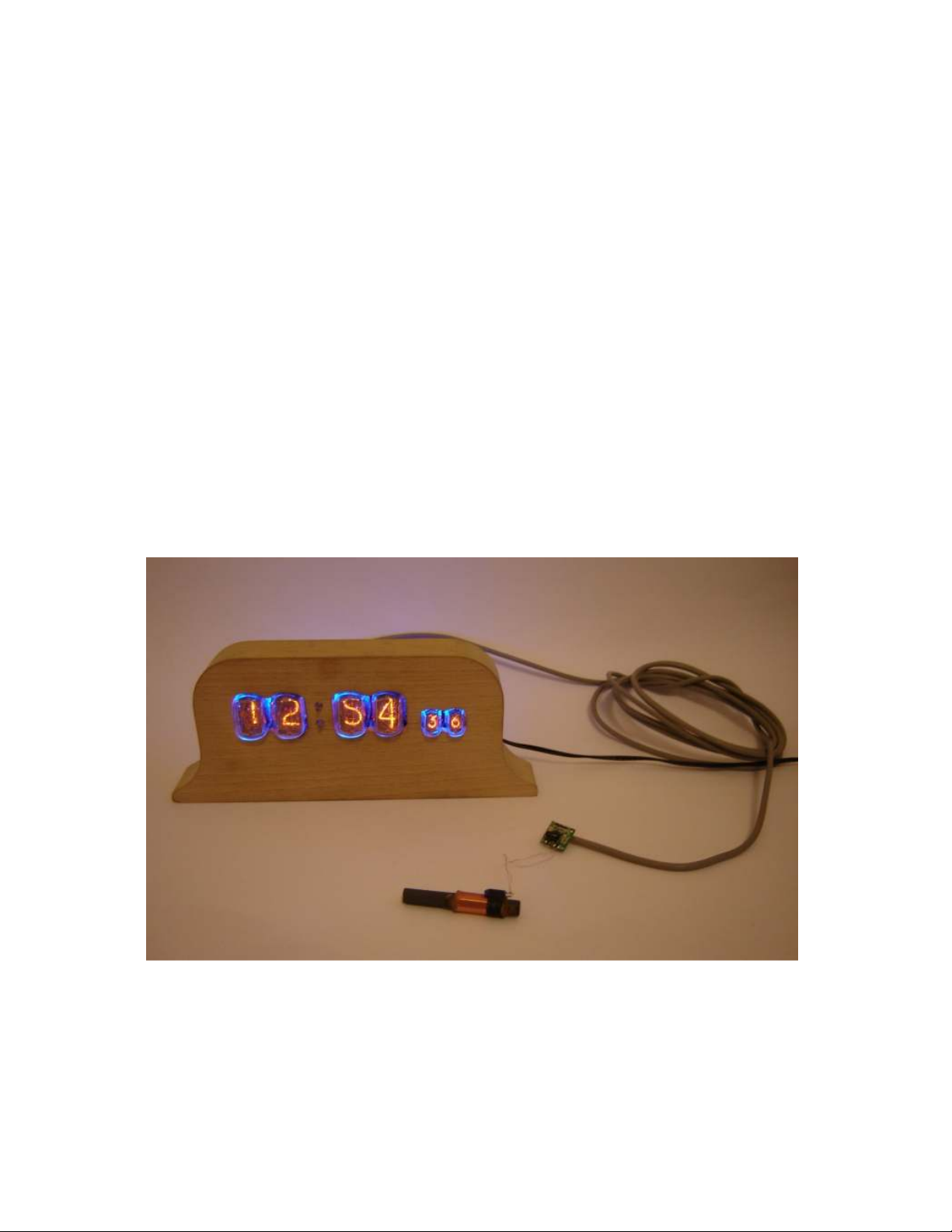
Nixie clock type ‘Frank 3’ is a compact design with all components and
tubes mounted on a single PCB. The efficient use of board space is
achieved by using a multiplex design to drive the display tubes. Only a
single high-voltage binary-to-decimal decoder IC (74141) is required,
and each tube is switched on in sequence very quickly to give the illusion
that all the tubes are actually lit.
The larger tubes for hours and minutes are type IN-12 with a digit height
of 18mm. The smaller tubes for the seconds are type IN-17 with a digit
height of 9mm. These tubes are Russian in origin and were produced
during the 1980’s, when the technology was at it’s most advanced. It is
expected that the tubes will last for very many years and should not need
replacing.
The optional wooden case and hardware pack (rear cover, screws),
supplied rough-machined, can be finished to give a very attractive clock
for everyday living spaces. The quality of the final finish will reflect the
time and care that is taken to finish the wood with successively finer
grades of sandpaper. Alternatively, you may wish to design your own
enclosure for the clock.
1.2 Clock Features
Nixie clock type ‘Frank 3’ has the following features:
- Hours, Minutes and Seconds display
- 12 or 24 hour modes
- Date display in either DD.MM.YY or MM.DD.YY format
- Alarm, with programmable snooze period
- Programmable date display each minute
- Attractive LED tube lighting
- Uses a Quartz Crystal Oscillator as the timebase
- Optional DCF/WWVB/ MSF/GPS synchronisation with status LED
- Supercapacitor backup. Keeps time during short power outages
- Simple time setting using two buttons
- Programmable leading zero blanking
- Five programmable neon colon settings (Flashing AM/PM indication,
illuminated AM/PM indication, both flashing, both on, both off)
- Seconds can be reset to zero to precisely the set time
- Programmable night mode - blanked or dimmed display to save tubes
or prevent sleep disturbance
- Separate modes for colon neons during night mode
- Standard or fading change of digits
- ‘Slot Machine’ Cathode poisoning prevention routine
- All user preferences stored to non-volatile memory
Nixie Tube Clock ‘Frank 3’
Issue 4 (30 Sept 2011)
www.pvelectronics.co.uk
Page 4

- 4
-
1.3 SAFETY
DANGER: The clock pcb includes a switched-mode voltage booster
circuit. This generates nominally 170 Volts DC, but is capable of
generating up to 300 Volts before adjustment. Assembly may only be
undertaken by individuals who are suitably qualified and experienced in
electronics assembly, and are familiar with safe procedures for working
with high voltages. If in doubt, refer to a suitably qualified engineer
before proceeding.
The voltages generated by this circuit can give a potentially
LETHAL ELECTRIC SHOCK.
DISCLAIMER: This product is supplied as a kit of parts, intended only for
suitably qualified electronic engineers, who are suitably qualified and
experienced in electronics assembly, and are familiar with safe
procedures for working with high voltages. The supplier, his agents or
associates accept no liability for any damage, injury or death arising from
the use of this kit of parts.
This is not a finished product, and the person assembling the kit is
responsible for ensuring that the finished product complies with any
applicable local regulations governing electrical equipment, eg. UL, CE,
VDE.
Nixie Tube Clock ‘Frank 3’
Issue 4 (30 Sept 2011)
www.pvelectronics.co.uk
Page 5
- 5
-
2. TOOLS AND EQUIPMENT REQUIRED
2.1 Tools required to assemble the PCB
The following tools will be required to assemble the PCB:
- Soldering iron with a small tip (1-2 mm)
- Wire cutters (TIP: A small pair of nail clippers works very well for this
function)
- Wire strippers (TIP: A small pair of scissors is quite suitable)
- Multimeter
- Small flat screwdriver for adjusting the high voltage supply
2.2 Materials you will need
Solder – lead / tin solder is preferred. Lead free solder, as now required
to be used in commercial products in Europe, has a much higher melting
point and can be very hard to work with.
Desoldering wick (braid) can be useful if you accidentally create solder
bridges between adjacent solder joints.
2.3 Other items you will need
The clock kit does not include a power adapter. This is because the kit is
sold to many countries around the world, each with very different
household mains outlet socket types. It is more efficient for the user to
buy a suitable adapter locally. This saves shipping a heavy adapter with
the kit, and also the extra costs of managing stocks of many varied
power adapters. If you are using a WWVB, DCF or MSF receiver avoid
cheap Chinese switching power supplies, as they can cause interference
problems.
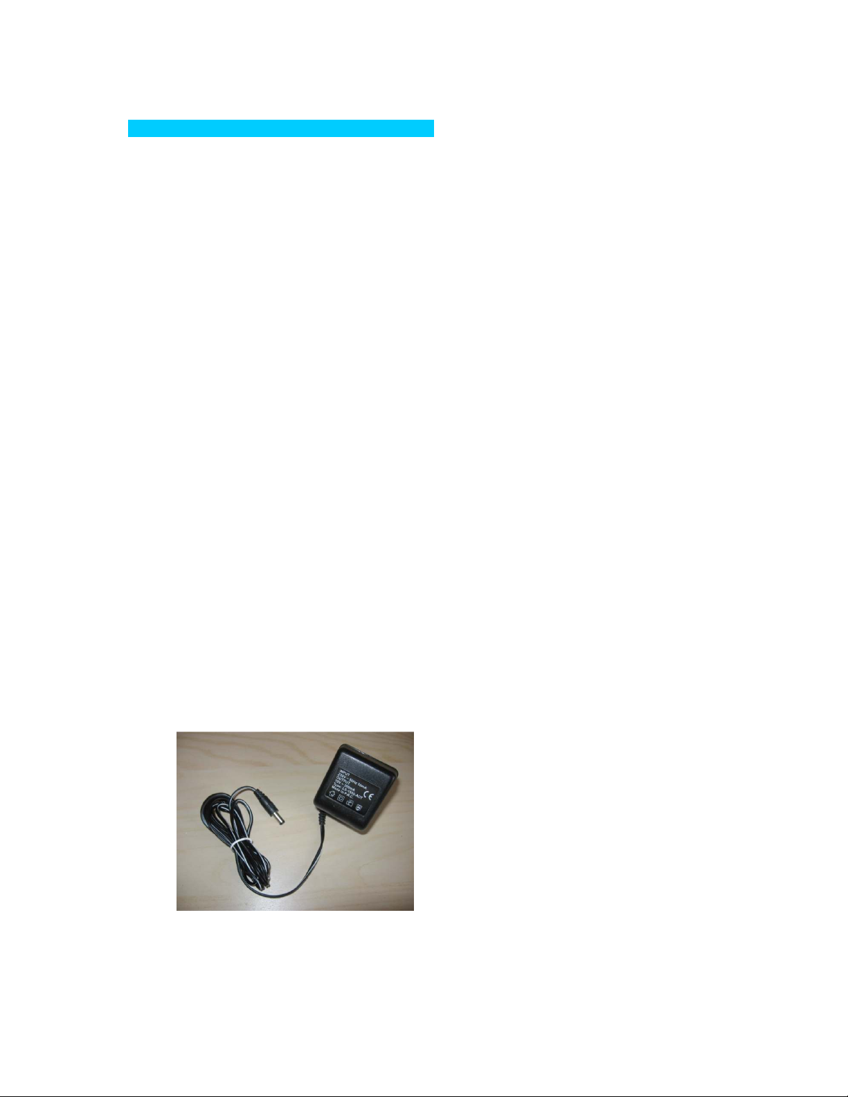
The type of power adapter can be obtained at very low cost. The
following type of adapter should be obtained and used with the kit:
Output 12V DC
Minimum power output capability of 250 mA
Output plug: 2.1mm pin, centre positive.
Nixie Tube Clock ‘Frank 3’
Issue 4 (30 Sept 2011)
www.pvelectronics.co.uk
Page 6
- 6
-
3. LIST OF COMPONENTS
Circuit Designation
Part Description
R5 – R7
560R, ¼ Watt
R20
– R25 390K, ¼ Watt
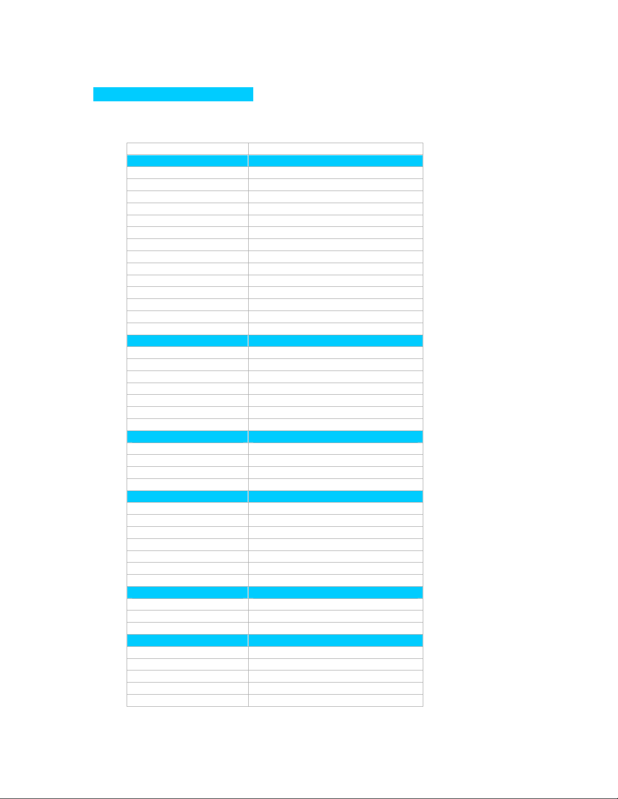
3.1 Table of components
Resistors
R1 390K, ¼ Watt
R2 4K3, ¼ Watt
R3 100R, ¼ Watt
R4 4K3, ¼ Watt
R8 - R10 10K, ¼ Watt
R11 560R, ¼ Watt
R12, R13 10K, ¼ Watt
R14 - R17 2K7, ¼ Watt
R18, R19 5K6, ¼ Watt
R26 – R33 10K, ¼ Watt
R34, R35 390K, ¼ Watt
R36 – R41 560R, ¼ Watt
Capacitors
C1 470uF, 16-25V, Electrolytic
C2 100uF, 16-25V, Electrolytic
C3 1uF, 250V, Electrolytic
C4 33pF Ceramic
C5 33pF Ceramic
C6 0.1F
C7 100nF Ceramic
Transistors
Q1 IRF730 or IRF630 MOSFET
Q2, Q3 MPSA42 NPN
Q4 – Q9 MPSA92 PNP
Q10 – Q18 MPSA42 NPN
Diodes
D1 – D3 1N5817 or 1N5819
D4 UF4004
D5 Not installed
D6 – D8 1N4148
D9 5mm Green LED
D10 5mm Orange LED
D11 – D16 3mm Blue LED
Integrated Circuits
IC1 7805 5V voltage regulator
IC2 PIC16F1936 8-bit microcontroller
IC3 74141 / K155N Nixie driver
Miscellaneous
L1 100uH – 220uH inductor
NE1, NE2 4mm wire ended neon lamp
SW1, SW2, SW3 Miniature vertical push button
VR1 1K Potentiometer
IC Socket 28 Way IC socket for IC2
Nixie Tube Clock ‘Frank 3’
Issue 4 (30 Sept 2011)
www.pvelectronics.co.uk
Page 7

- 7
-
J1 2.1mm Chassis power socket
GPS / RFT 6 way mini DIN PCB socket
LS1 Piezo sounder
FUSE 500mA fuse
SKT1-44 1mm PCB Sockets
Insulation Clear insulation for neons
X1 32.768KHz watch crystal
The resistors used in the kit are 1% tolerance metal film. They are
marked with 4 coloured bands to identify the value. However it is
sometimes unclear in which direction the bands should be read.
Therefore, we recommend that the resistors be identified with a
multimeter.
Nixie Tube Clock ‘Frank 3’
Issue 4 (30 Sept 2011)
www.pvelectronics.co.uk
Page 8
- 8
-
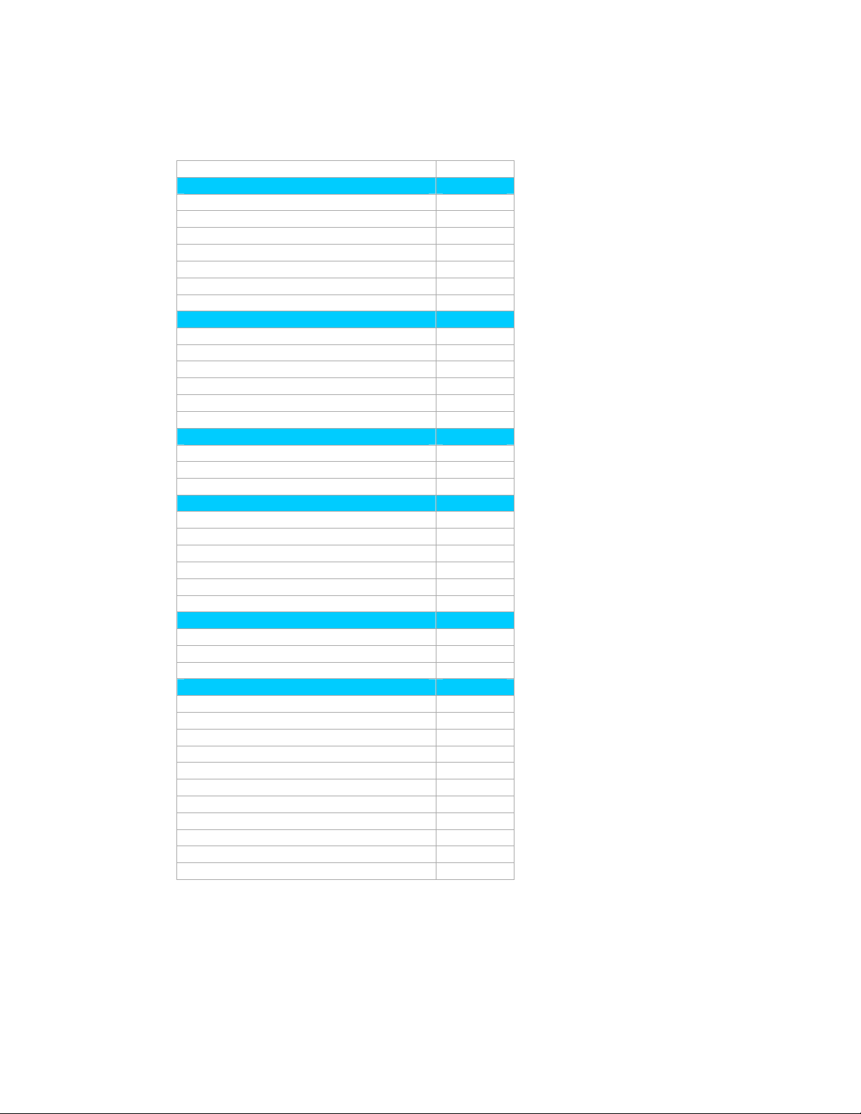
3.2 Parts list / Packing sheet
IRF730 or IRF630 MOSFET
1
Diodes
Part Description Quantity
Resistors
100R, ¼ Watt 1
560R, ¼ Watt 10
2K7, ¼ Watt 4
4K3, ¼ Watt 2
5K6, ¼ Watt 2
10K, ¼ Watt 13
390K, ¼ Watt 9
Capacitors
470uF, 16-25V, Electrolytic 1
100uF, 16-25V, Electrolytic 1
1uF, 250V, Electrolytic 1
100nF, Ceramic 1
33pF, Ceramic 2
0.1F 1
Transistors
MPSA92 PNP 6
MPSA42 NPN 11
1N581x 3
UF4004 fast recovery diode 1
1N4148 3
5mm Green LED 1
5mm Orange LED 1
3mm Blue LED 6
Integrated Circuits
7805 5V voltage regulator 1
PIC16Fxxxx 8-bit microcontroller 1
74141 / K155N Nixie driver 1
Miscellaneous
100uH – 470uH inductor 1
4mm wire ended neon lamp 2
Miniature vertical push button 3
1K potentiometer 1
28 way IC Socket for IC2 1
2.1mm Chassis power socket 1
6 way mini DIN PCB socket 1
Piezo sounder 1
500mA fuse 1
6 cm clear insulation 1
32.768KHz watch crystal 1
It is recommended that the kit is checked against the list above, to
ensure all parts are present before commencing assembly. Don’t be
alarmed if there are some extra components, as some component
bags are shared between different kit types.
Nixie Tube Clock ‘Frank 3’
Issue 4 (30 Sept 2011)
www.pvelectronics.co.uk
Page 9
- 9
-
4. ASSEMBLY OF THE PCB
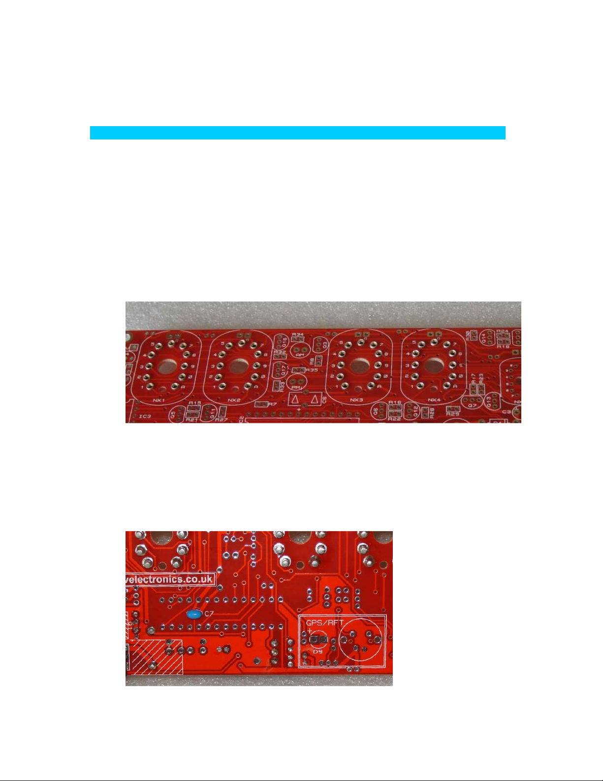
4.1 1mm Sockets For Nixie Tubes
There are 44 individual sockets that need to be soldered in. The
best method is a follows. Place all sockets into the holes, noting
that for each tube there is one hole that has no socket as show
below. When all sockets have been placed, place a flat and hard
object over the top of the sockets, and turn the PCB over so you
can solder from the underside. Be sure to insert the sockets FROM
the component side of the PCB – the side with the white
component markings. The photo below shows the component side
of the PCB after all the sockets have been inserted and soldered in.
4.2 Capacitor C7
Mount C7 on the same side of the PCB as the white cross-hatched
markings for Q1 and IC1. See below.
Clip the leads on the main component side very short, as the IC
socket for IC2 will need to fit over the trimmed leads.
Nixie Tube Clock ‘Frank 3’
Issue 4 (30 Sept 2011)
www.pvelectronics.co.uk
Page 10
- 10 -
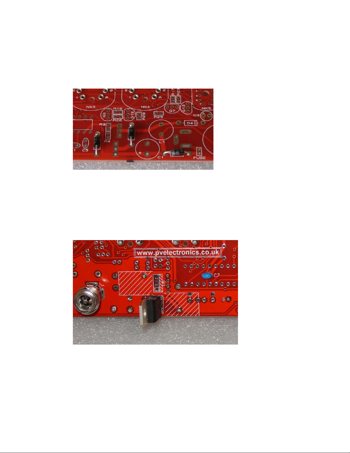
4.3 Low Voltage Power components:
J1, FUSE, D1-D3, IC1, C1, C2
Start by installing D1-D3. Align the white band on the components
with the band marked on the PCB.
Continue to mount C1, C2, J1 and FUSE Note that C1 and C2 are
polarised. The longer lead goes in the hole marked (+). J1, the DC
power input connector and IC1 are mounted on the opposite side of
the PCB to the other components in this step.
See the picture below. IC1 is mounted vertically at this stage - do
not bend it over the marked area yet.
Nixie Tube Clock ‘Frank 3’
Issue 4 (30 Sept 2011)
www.pvelectronics.co.uk
Page 11
- 11 -
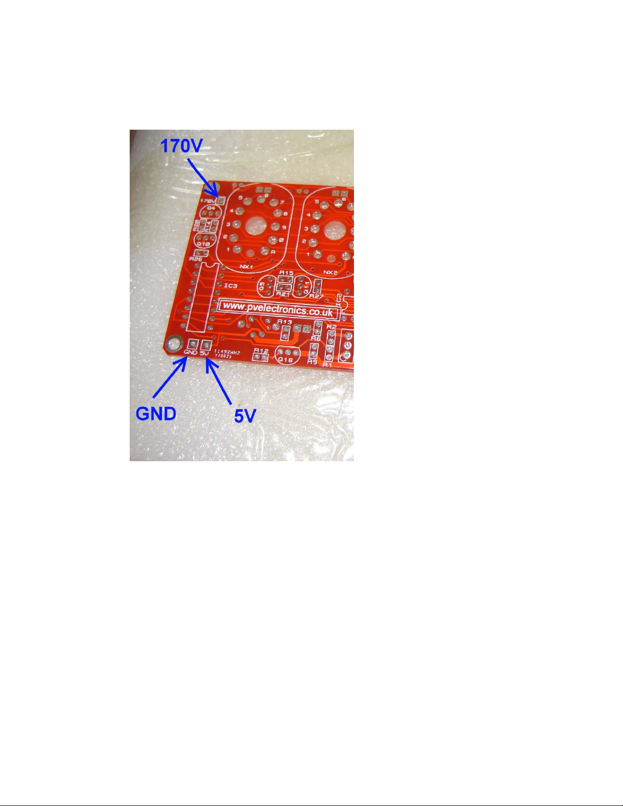
4.4 Testing Stage 1 Power Components.
Identify the test GND, 5V and 170V test points as shown below.
Plug in the power supply, and then test using a DC voltmeter or a
multimeter on DC setting: Touch the black probe on the GND test
point and the red probe on the 5V test point. The voltage should
measure between 5.1 and 5.3 Volts. If not, disconnect power and
check your work. Do not proceed with the assembly until the error
is corrected. Once the test is completed, disconnect the power.
4.4 High Voltage Generator components.
R1, R2, R3, R4, R9, R10,
Q1, D4, C3, VR1, L1, Socket for IC2
Pay attention to mount D4 with the white band aligned with the
PCB marking. Insert the 28 way IC socket into the PCB at the IC2
position, ensuring that the notch at one end is aligned with the
corresponding marking on the PCB.
Nixie Tube Clock ‘Frank 3’
Issue 4 (30 Sept 2011)
www.pvelectronics.co.uk
Page 12
- 12 -
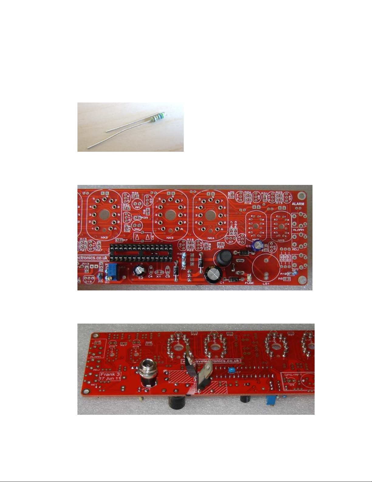
Resistors R1-R4, R9 and R10, indeed all the resistors on the board
need to be mounted upright to save space. The leads need to be
formed as shown below. Bend the leads of each resistor as shown
and solder in to the correct postion, making sure the component
body is as close to the board as possible.
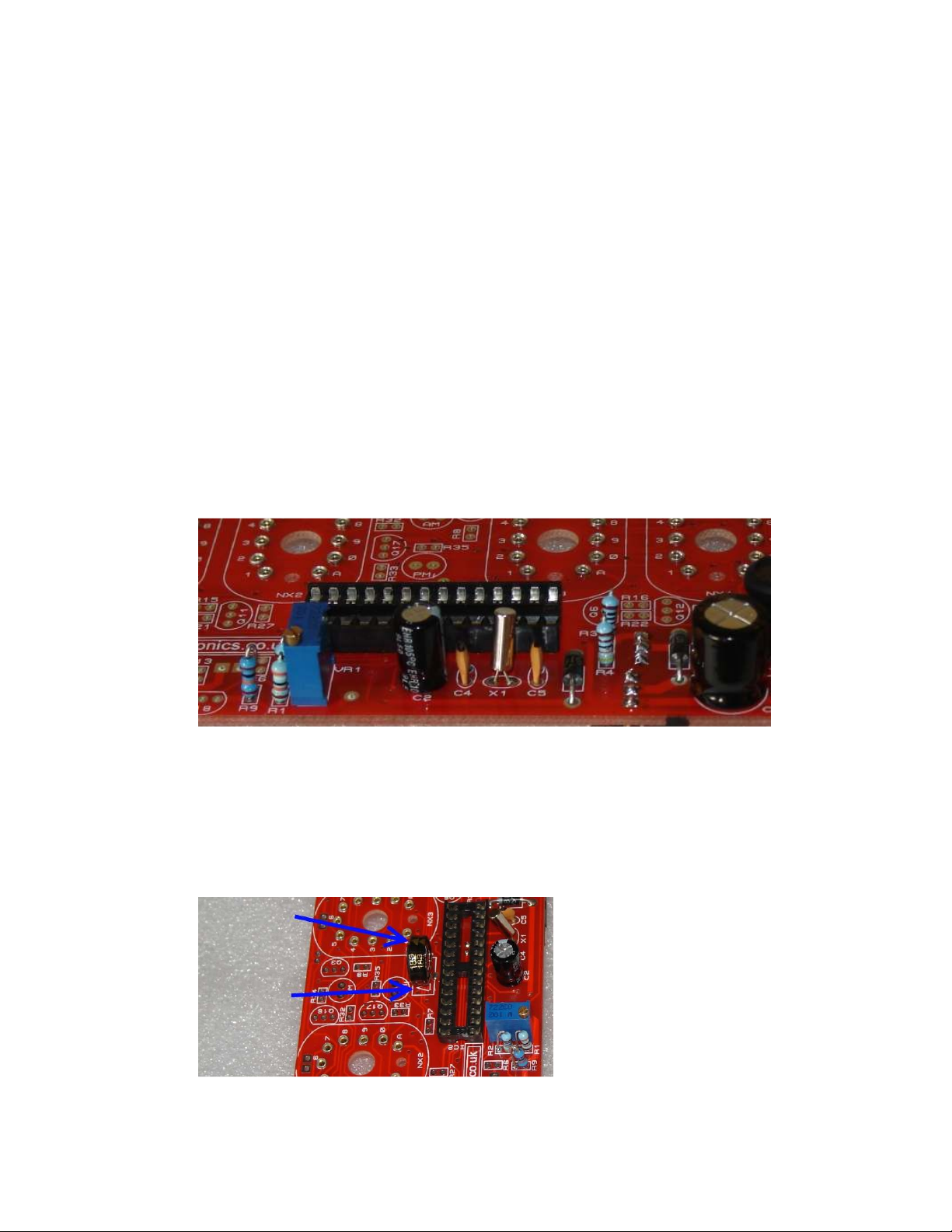
After installation of step 4.4 components, this is how the PCB
should look on the component side:
And this is the view on the ‘solder side’ – note that Q1 is mounted
on this side.
Nixie Tube Clock ‘Frank 3’
Issue 4 (30 Sept 2011)
www.pvelectronics.co.uk
Page 13
- 13 -
4.5 High Voltage Generator Test.
- Refer to the warnings on page 4
- Insert IC2 into its socket. Orient the notch on the IC with the
notch on the IC socket and the PCB marking.
- Power up the PCB, and using the GND and 170V test points,
measure the high voltage generated using a multimeter or
voltmeter on DC setting.. It should be initially between 150 and
190V. Using the VR1 brass screw, slowly adjust the screw until the
voltage is between 170 and 175V. Disconnect the power supply.
- Finally, remove IC2 from its socket and replace on its staticprotective foam. It is best kept safe until needed for the tube tests
later in the assembly.
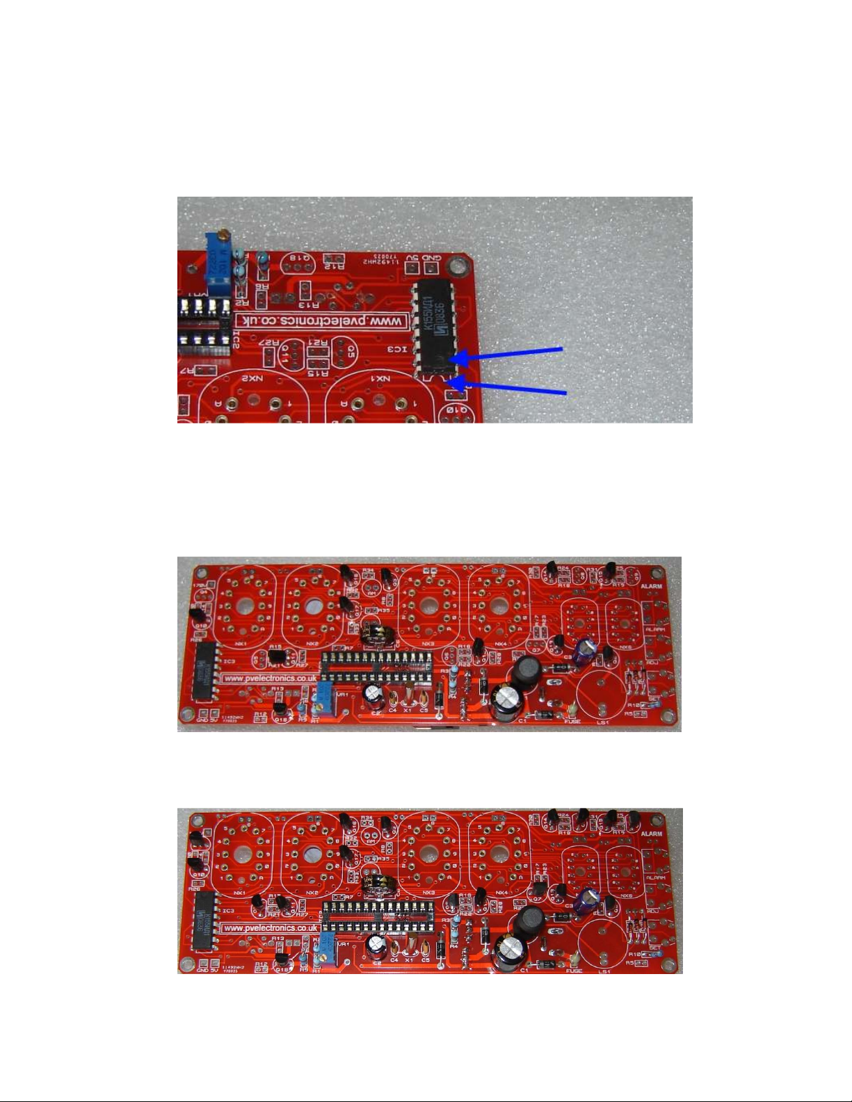
4.6 C4, C5, X1.
These are the timekeeping components: 32.768KHz crystal and
two load capacitors. See below:
4.7 D6 - D8, C6.
C6 is a high capacity ‘Super Capacitor’, intended to keep the
processor powered for short periods in the event of a main power
failure. It is vital that it is placed in the correct orientation. See
below. There are arrows on the component that need to be
pointing the same way as the arrows on the PCB.
Nixie Tube Clock ‘Frank 3’
Issue 4 (30 Sept 2011)
www.pvelectronics.co.uk
Page 14
- 14 -
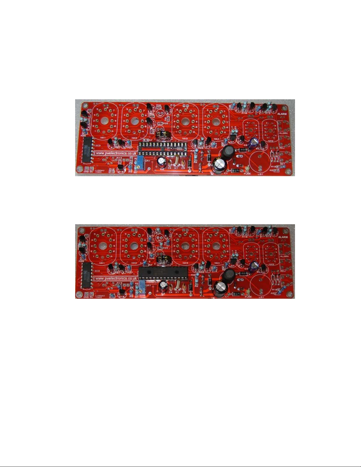
4.8 IC3 – 74141 / K155N Nixie Driver IC.
Align the notch on the IC body with the corresponding PCB mark.
See below:
4.9 Q2, Q3, Q10 – Q18 (All MPSA42)
After placement of these 11 transistors, the board should look like
this:
4.10 Q4 – Q9 (All MPSA92)
See below:
Nixie Tube Clock ‘Frank 3’
Issue 4 (30 Sept 2011)
www.pvelectronics.co.uk
Page 15
- 15 -
4.11 R14 – R17 (2K7)
R18, R19 (5K6)
R20 – R25 (390K)
R26 – R31 (10K)
See picture below:
4.12 R12, R13, R32, R33 (10K)
R34, R35 (390K)
R8 (10K), R5, R6, R7, R11 (560R)
See picture below:
Nixie Tube Clock ‘Frank 3’
Issue 4 (30 Sept 2011)
www.pvelectronics.co.uk
Page 16
- 16 -
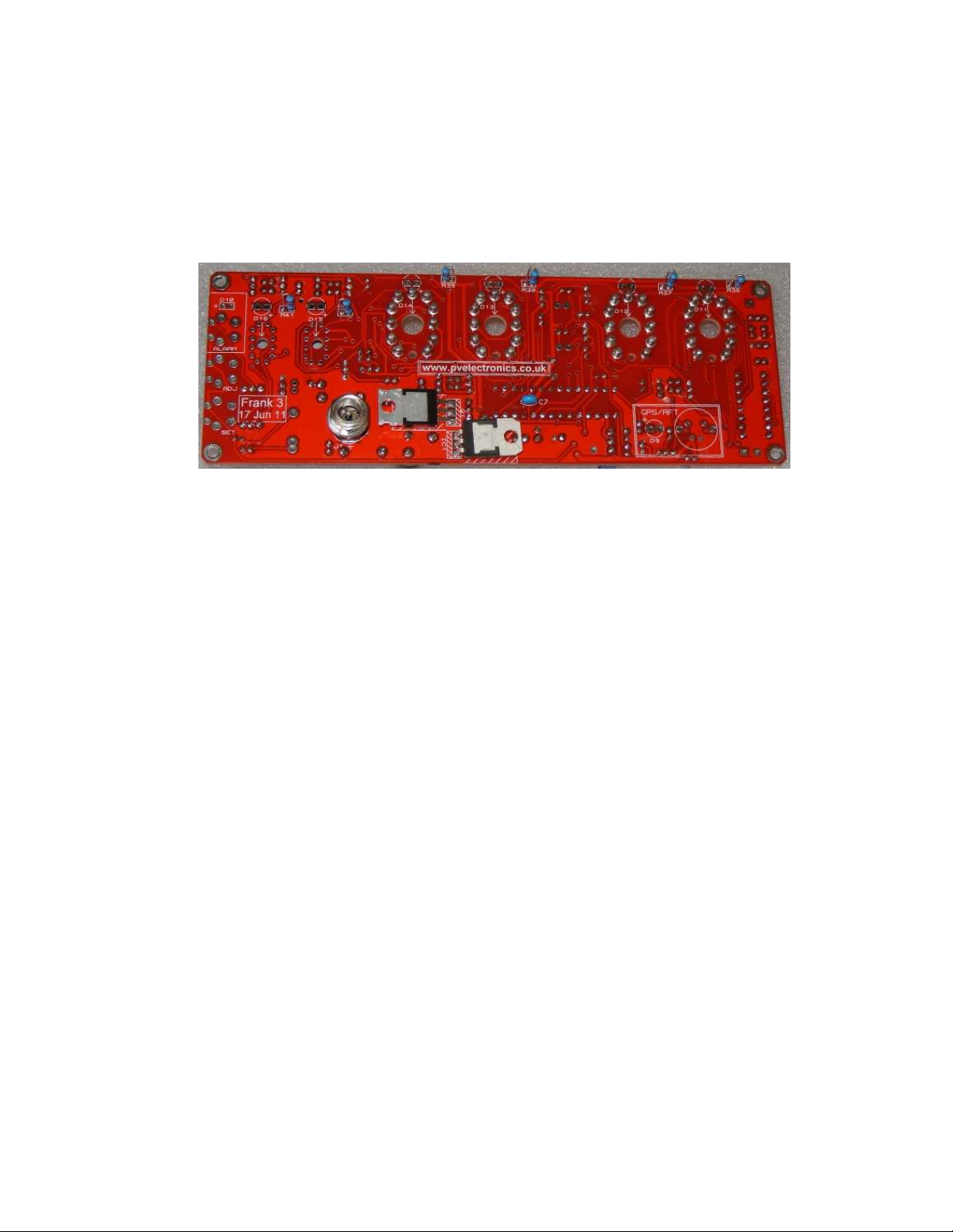
4.13 R36 – R41 (560R)
These are the current-limiting resistors for the LED tube
underlights. If you don’t want to have LED tube underlighting you
can omit this step. Note that you can also now bend back Q1 and
IC1 as shown below:
Nixie Tube Clock ‘Frank 3’
Issue 4 (30 Sept 2011)
www.pvelectronics.co.uk
Page 17
- 17 -
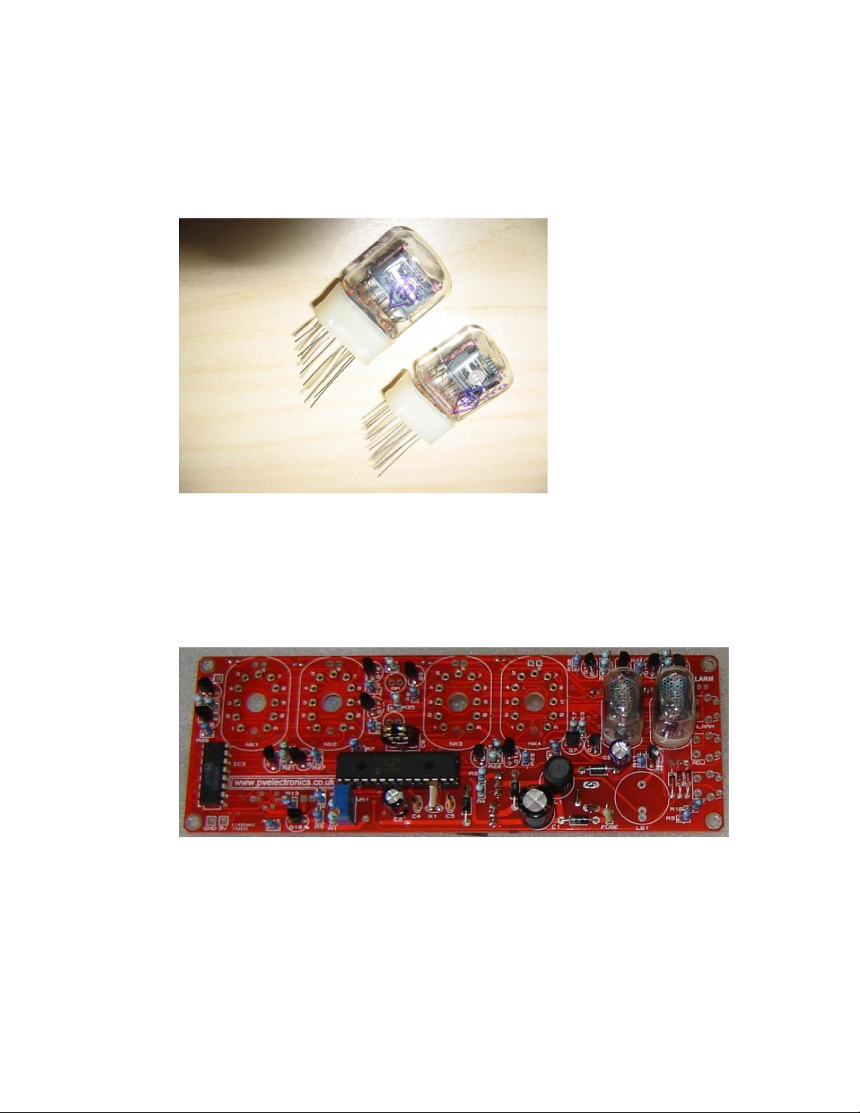
4.14 IN-17 Nixie tubes NX5, NX6
To facilitate easy insertion of the flying leads into the small holes, it
helps enormously to trim the flying leads at an angle with a pair of
scissors as shown below
Feed all the wires in progressively. It is not as hard as it seems at
first. Ensure the tubes are the correct way up. The part marking
IN-17 should be to the RIGHT, but also check to see if you can tell
that the 5 and 3, which are visible, are the correct way up. After
soldering in, trim flying leads.
Nixie Tube Clock ‘Frank 3’
Issue 4 (30 Sept 2011)
www.pvelectronics.co.uk
Page 18
- 18 -
4.15 SET, ADJ, ALARM
Push buttons SET, ADJ and ALARM are mounted on the solder side
of the PCB, so that the clock is adjusted from the back. You can
choose to mount them on the front face if you wish, depending on
your own particular clock case design.
4.16 NE1, NE2
The 2 neons can now be mounted at a suitable height. Use small
lengths of the clear insulation supplied on the leads to prevent
shorts.
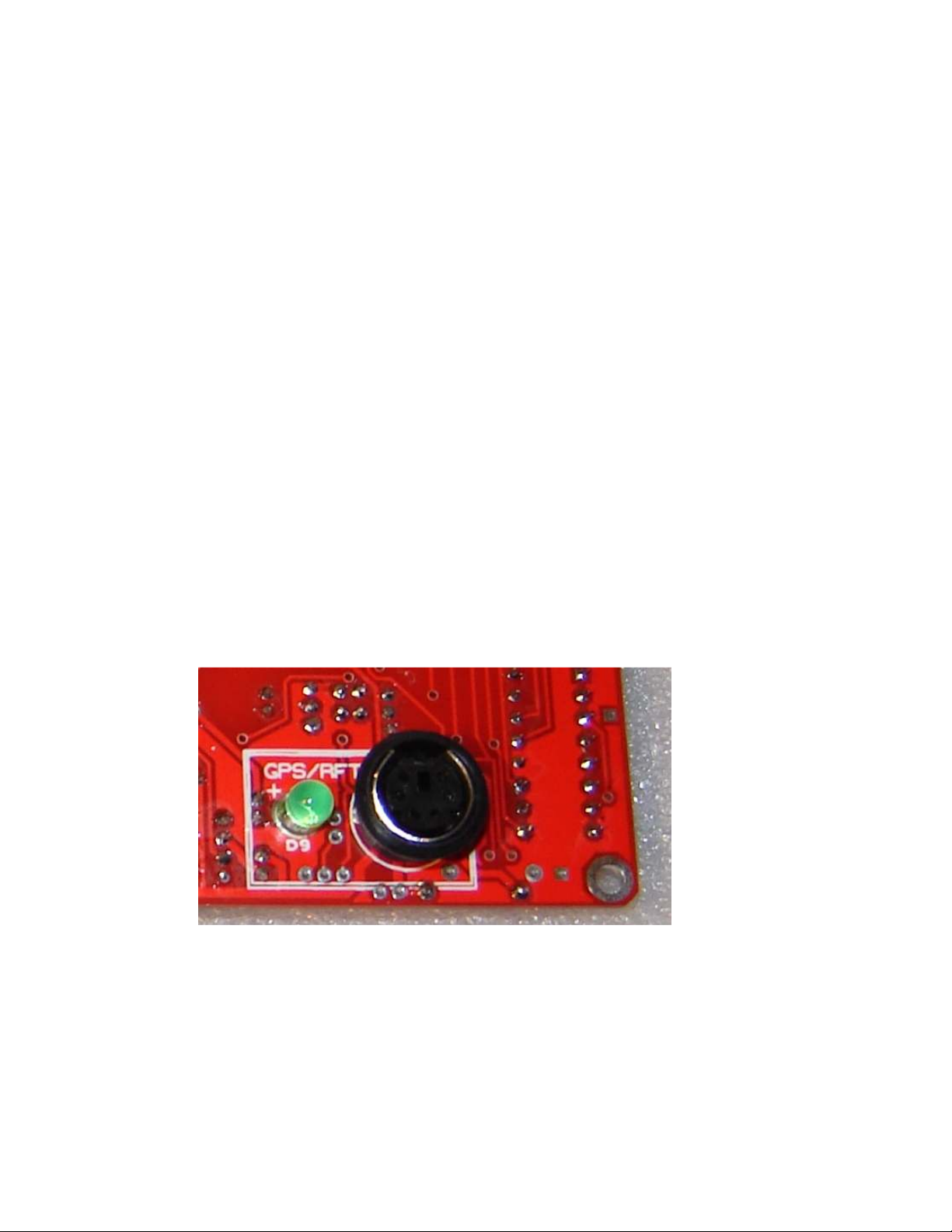
4.17 RFT/GPS LED D9 (Green)
ALARM LED D10 (Orange)
These should be mounted on the solder side of the PCB if you are
using one of our cases. Otherwise they can be mounted as you
prefer. The longer leads go into the holes maked (+)
4.18 RFT / GPS Connector.
If you will not be using a time synchronisation source, you may
omit this connector. Also, if you are connecting a time receiver
module close to the clock PCB without using the connector you
may omit this connector.
The connector is mounted on the solder side of the PCB:
The connector is a tight fit into its holes, It may be necessary to
place the PCB on a flat surface and push the connector into place
with your thumb. Then solder the 6 pins and the 2 guide pins.
Nixie Tube Clock ‘Frank 3’
Issue 4 (30 Sept 2011)
www.pvelectronics.co.uk
Page 19

- 19 -
4.19 LS1 – Piezo Sounder.
There are two sets of holes for this component, as two different
types may be supplied depending on component availability.
If you are using one of our cases, mount this on the solder side of
the PCB.
Nixie Tube Clock ‘Frank 3’
Issue 4 (30 Sept 2011)
www.pvelectronics.co.uk
Page 20
- 20 -
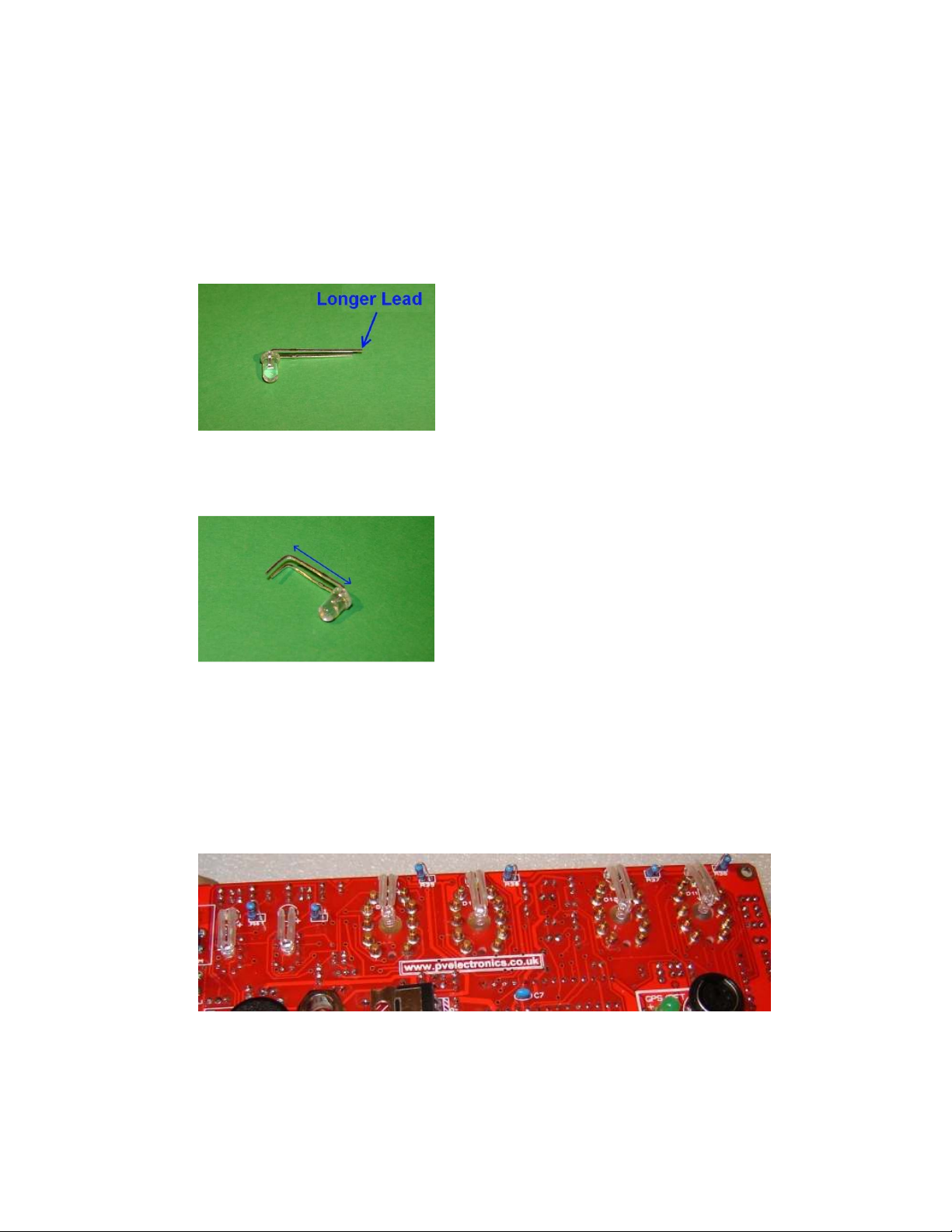
4.20 D11 – D16 (3mm Blue LED).
You can substitute other colour 3mm LEDs if you wish.
Bend the leads of each LED as shown below. Note that the longer
(+) lead is on the top. This is important as the leads will be
trimmed to the same length, so you need to be sure that you have
the correct (longer) lead in the (+) hole.
Now bend again, appropriate to the spacing between the pads for
the LED and the hole for the LED. Cut the leads to the same
length:
The six LEDs may now be installed, as shown below. Insert and
solder on the solder side. Take care that the LED leads are well
clear of the tube leads and sockets. If you wish you may use some
short pieces of insulation as shown to prevent the possibility of any
LED leads touching the tube sockets or leads, but this should not
be necessary if you take care to bend the LED leads to the correct
dimensions.
The LED positions may need to be adjusted to give a uniform
appearance when viewed from the front.
Nixie Tube Clock ‘Frank 3’
Issue 4 (30 Sept 2011)
www.pvelectronics.co.uk
Page 21

- 21 -
5. TESTING THE CLOCK
5.1 Prepare for first test.
Install IC2 into its socket.
Insert NX1 – NX4.
5.2 First Power-up with tubes
Ensuring that the push button switches are clear of any obstruction
that could press them, power up the clock.
The tubes should start counting 0-9 repeatedly.
If any tubes do not light, disconnect power and trace the fault
before proceeding.
To exit tube test routine, press ‘SET’ briefly. The clock will go into
time display mode starting from 12:34 pm
Nixie Tube Clock ‘Frank 3’
Issue 4 (30 Sept 2011)
www.pvelectronics.co.uk
Page 22

- 22 -
6. HOW TO OPERATE THE CLOCK
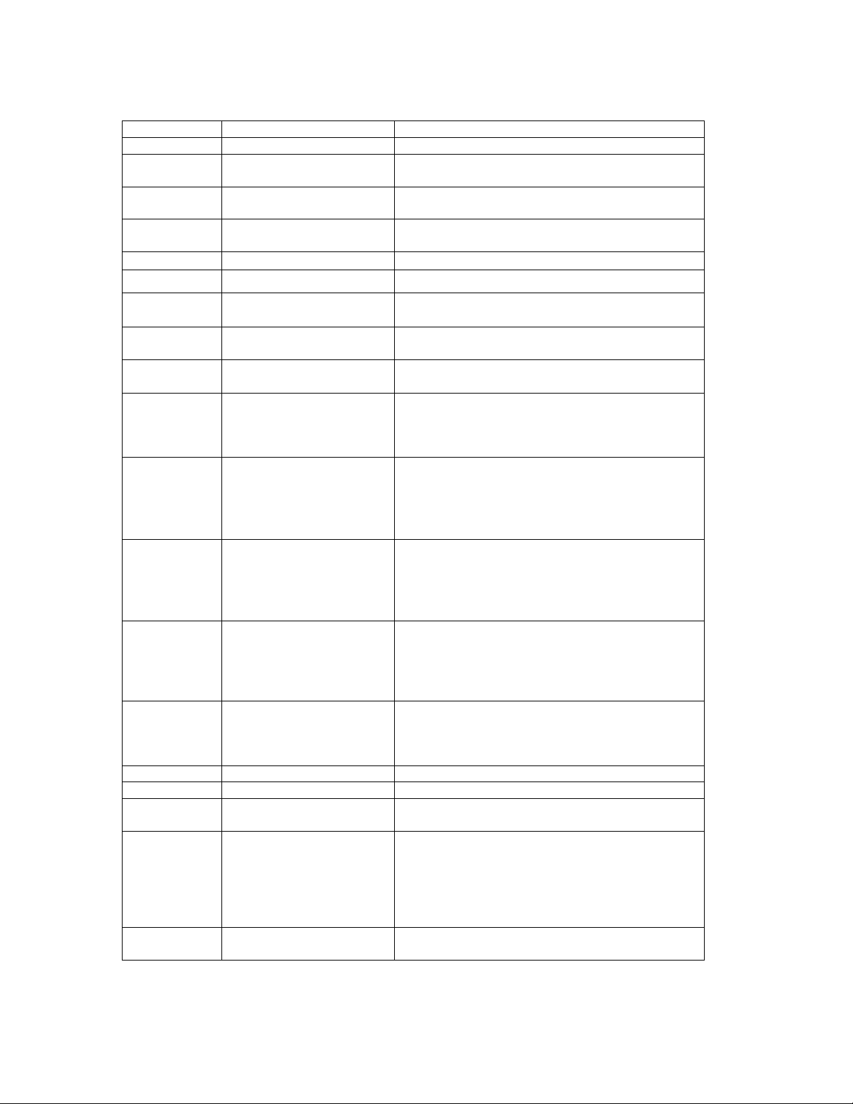
The three buttons have the following functions:
SET: Exit tube test routine on cold power-up;
Show date;
Set: time, date;
Enter configuration menu;
ADJ: Call WWVB / DCF / MSF;
Adjust: time, date, alarm time, configuration parameters;
ALARM: Set alarm time; snooze; cancel snooze/alarm;
Entering configuration mode:
The principal settings of the clock are stored in flash memory – your
preferred configuration is stored even after powering off the clock for
extended periods. To access the configuration mode press and hold the
‘Set’ button. After 2 seconds the seconds will become highlighted.
Continue holding the button a further 2 seconds until the clock displays
in this format:
99.
00-XXconfiguration menu.
The ‘99’ in the seconds digits tells you that you are in the
In configuration mode the hours digits diplay the current parameter
being adjusted, and the seconds digits display the current value stored
against the parameter.
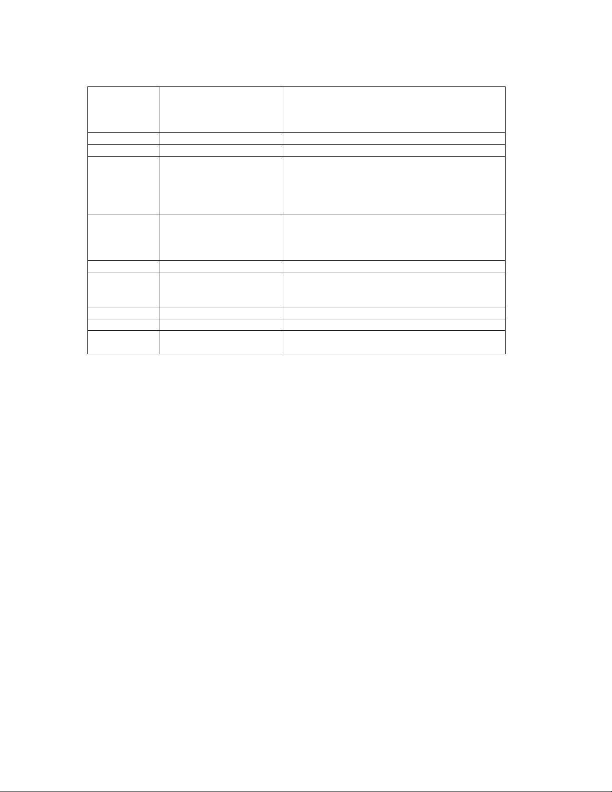
For each parameter, and referring to the table below, scroll through the
range of possible values by pressing the ‘ADJ’ button. When the desired
value has been reached, move on to the next parameter by pressing the
‘SET’ button. When the last parameter has been set, pressing ‘SET’ one
more time will revert the clock back to time display mode. The first
parameter (0) cannot be changed as it is the software revision number.
It will show for several seconds and then move to parameter 1.
In all correspondence on support issues, please quote the board type,
revision date and software version.
Nixie Tube Clock ‘Frank 3’
Issue 4 (30 Sept 2011)
www.pvelectronics.co.uk
Page 23
- 23 -
Parameter Description Values
1
3 –
15 minutes
3
0 Software revision 30 = version 3.0, 31 = version 3.1 etc
1 12 / 24 Hr mode 0 – 12 Hr (default)
1 – 24 Hr
2 Date format 0 = MM.DD.YY (default)
1 = DD.MM.YY
3 Leading zero blanking
eg. 01:54:32
0 – leading zero blanked (default)
1 – leading zero displayed
4 Night mode start hour 0 - 23
5 Night mode end hour 0 - 23
6 Night mode 0 – Tubes off (default)
1 – Dimmed display
7 Display mode 0 – standard change of digits(default)
1 – fading digits
8 Night mode override
0 – 50 (default 3)
period (minutes)
9 Snooze period 0 – 6 minutes (default)
1 – 9 minutes
2 – 12 minutes
10 Colon neons mode 0 – AM/PM Indication, flashing
1 – AM/PM Indication, illuminated
2 – Both flash (default)
3 – Both illuminated
4 – Both off
11 Colon neons during
night dimmed mode
0 – AM/PM Indication, flashing
2
1 – AM/PM Indication, illuminated
2 – Both flash
3 – Both illuminated (default)
4 – Both off
12 Radio time signal
source
0 – No Radio Time source (default)
1 – DCF
2 - WWVB
3 – MSF
4 - GPS
13 GPS Baud rate 0 – 4.8 Kbps (default)
1 – 9.6 Kbps
2 – 19.2 Kbps
3 – 38.4 Kbps
14 Radio time offset hours 0-13 (default 0)4
15 Radio time offset mins 0-45 (default 0)4
16 Radio time offset
polarity
17 WWVB Auto DST
Disable /Set DST in
GPS mode
0 - minus time (default)
1 – plus time
WWVB Sync Mode:
0 –Auto DST on WWVB Sync (default)
1 – Disable Auto DST on WWVB Sync
GPS Sync Mode:
18 Auto date display each
minute
0 – No DST offset
1 – 1 hour DST offset
0 – Off
1 – On (default)
6
7
5
Nixie Tube Clock ‘Frank 3’
Issue 4 (30 Sept 2011)
www.pvelectronics.co.uk
Page 24
- 24 -
19 LED backlights 0 - Always off
1 - Always on
2 - On, and follows tube nightblanking
(default)
20 Reserved – leave as 0 0
21 Reserved – leave as 0 0
22 Slots Mode8 0 – Slots disabled
1 – Slots every minute
2 - Slots every 10 minutes (default)
3 - Slots every hour
4 – Slots at midnight
23 RFT Sync Mode9
24 RFT Daily Sync Hour 0 – 23 (default 2)
25 RFT Seek Blanking 0 – Keep tubes lit for DCF / WWVB / MSF
26 Reserved – leave as 0
27 Reserved – leave as 0
28 Restore default settings 0 – Keep user settings
0 – DCF / WWVB / MSF Sync once per day
only as per parameter(24)
1 – DCF / WWVB / MSF Sync every hour
(default)
seek (default)
1 – Blank tubes for DCF / WWVB / MSF seek
10
1 – Restore original default settings
Notes:
1. Press ‘SET’ briefly during blanking to show time for prescribed period.
2. Night time neons mode is active when night mode is set to dim. During night time
blanking the tubes AND neons are disabled.
3. Clock is fully functional without WWVB / DCF / MSF / GPS synchronisation. Set time
manually.
4. Enter your time zone offset from the synchronisation source. Note that WWVB
transmits UTC.
5: Set this to ‘1’ to disable Auto DST adjust on WWVB Sync – eg. Arizona does not
observe DST. Only active in WWVB Sync mode.
6. In GPS Sync mode, this parameter is used to set DST. Set to ‘1’ during DST.
7. Date will be displayed each minute between 50 and 55 seconds past the minute.
8. Visual effect / cathode poisoning prevention – all digits on all tubes are cycled for 10
seconds.
9. DCF / WWVB /MSF synchronisation takes place on the hour. If no valid frame is
received in 6 minutes, the clock reverts to normal operation.
10. Set this parameter to ‘1’ to restore original default settings. Internal operations will
then load all the original settings and restore the value to ‘0’
Nixie Tube Clock ‘Frank 3’
Issue 4 (30 Sept 2011)
www.pvelectronics.co.uk
Page 25

- 25 -
Setting the Time and Date:
From time display mode, press and hold ‘SET’ button for 2 seconds until
the seconds digits are highlighted.
Press the ‘ADJ’ button to reset seconds to zero.
Briefly Press ‘SET’ again and the hours will be highlighted
Press the ‘ADJ’ button to set the minutes.
Briefly Press ‘SET’ again and the hours will be highlighted.
Press the ‘ADJ’ button to set the hours.
Proceed in this fashion to set the calendar: Year, Month and Day.
Finally, briefly Press ‘SET’ again to revert to normal clock operation.
Showing Date:
From time display mode, briefly press ‘SET’ button. Date will be shown
for 5 seconds, then revert to time display.
Auto Date Display:
Setting parameter (18) to ‘1’ will enable auto display of date between 50
and 55 seconds past each minute.
Night Blanking Override:
During programmed night blanking, the blanking may be overridden to
see the time by briefly pressing the ‘SET’ button. Tubes will remain lit for
the period defined in parameter (8).
Manual RFT Call:
In DCF / WWVB / MSF modes, pressing ‘ADJ’ briefly during time display
will initiate a manual time seek for maximum 6 minutes, or until a valid
time frame is received.
Setting Alarm:
Press the ‘ALARM’ Button. The seconds digits show the on / off status of
the alarm: 00 or 01 (off or on).
Set on / off status, then minutes followed by hours by using the ‘ALARM’
and ‘ADJ’ buttons. When set, the alarm LED will also light.
Canceling Alarm:
Press ‘ALARM’ briefly to cancel alarm and enter snooze mode, or a longer
press until the clock bleeps, to cancel snooze. Alarm remains set for the
next day.
Nixie Tube Clock ‘Frank 3’
Issue 4 (30 Sept 2011)
www.pvelectronics.co.uk
Page 26

- 26 -
7. USING A RADIO FREQUENCY TIME RECEIVER OR GPS
RECEIVER
The clock can automatically synchronise time from DCF (Europe),
WWVB (USA), and MSF (UK) long wave time transmitters.
The clock can also receive time from a GPS receiver that transmits
information using NMEA-0183 protocol, using the $GPRMC
sentence.
7.1 Configuring for RFT or GPS Synchronisation.
• Set parameter 12:
1: DCF
2: WWVB
3: MSF
4: GPS
• If using GPS, set the baud rate in parameter (13)
• Set parameters 14 and 15 for the hours and minutes your time
zone is offset from the synchronisation source. This is usually
only whole hours. Examples:
o Eastern USA is 5 hours offset from UTC transmitted by the
WWVB transmitter.
o UK is 1 hour offset from the time transmitted by the DCF
transmitter
o France has no offset from the time transmitted by the DCF
transmitter
• Set parameter (16) to identify whether the offset is minus (0) or
positive (1) of the time source.
• If using WWVB source, and you do NOT require automatic DST
adjustment (eg. Arizona does not observe DST), then set
parameter (17) to 1.
• If using GPS, parameter (17) acts as a DST bit. Set to 1 during
DST period, and 0 during standard time period.
• Set parameter (23) to select between hourly seek and daily
seek in DCF / WWVB / MSF modes.
• If you have selected daily seek, use parameter (24) to set the
time of the daily seek in DCF / WWVB / MSF modes.
• If you intend to place the RFT receiver module closer to the
clock PCB than 6 ft / 2 metres, the clock will need to disable HV
and switch off the tubes for time seek, otherwise the switchmode power supply will prevent reception. Select blanking
during time seek by setting parameter (25) to 1. Leave as 0 to
keep tubes lit during time seek.
Nixie Tube Clock ‘Frank 3’
Issue 4 (30 Sept 2011)
www.pvelectronics.co.uk
Page 27
- 27 -
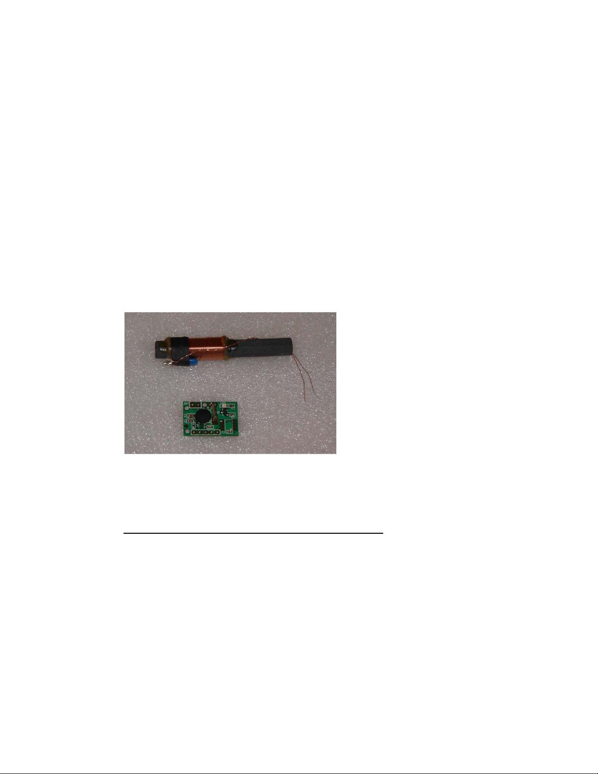
7.2 DCF / WWVB / MSF Synchronisation.
An optional receiver and 3 metre cable is available. The Radio
Frequency Time (RFT) receiver module plugs into the mini-DIN
socket on the rear of the PCB.
7.3 Connecting the DCF / WWVB / MSF receiver.
The clock is designed to be used with Symtrik RFT time receiver
module type SYM-RFT-xx
These modules feature an on-board indicator LED to indicate the
regular pulses from the time transmitter. This is very useful in
setting up the module, to determine if a good signal has been
found. The modules output coded time information in inverted
format and this is the format the clock can decode.
An additional feature of the modules is the PON pin, which is used
to place the module is an ultra low power standby mode when not
being used for time seek.
If you are using our module and 3 metre extension cable, proceed
to step 8.4. If you are wiring in the module close to the main clock
PCB or by direct soldering to the clock PCB pads, refer to step 8.5.
Some Notes on WWVB / DCF / MSF Reception:
Many other electrical applicances such as TVs and Mobile phones
reception when in close proximity. Metal objects cause reception
problems too. It is suggested to start off with the antenna by a
window, in the approximate direction of the signal Do not point the
antenna at the direction of the signal, but have the antenna sideon to the signal direction.
Once a good signal has been obtained, try different locations, and
progressively further from the window.
Place and design your case so the antenna is as far away from the
PCB as possible.
Nixie Tube Clock ‘Frank 3’
Issue 4 (30 Sept 2011)
www.pvelectronics.co.uk
Page 28
- 28 -
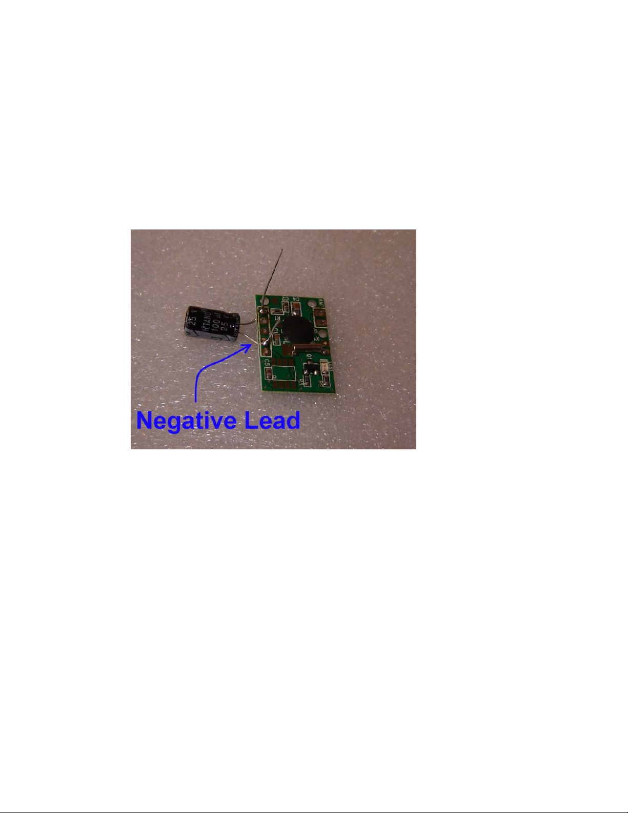
7.4 Making up the RFT Module and cable.
Make connections to the RFT module as follows:
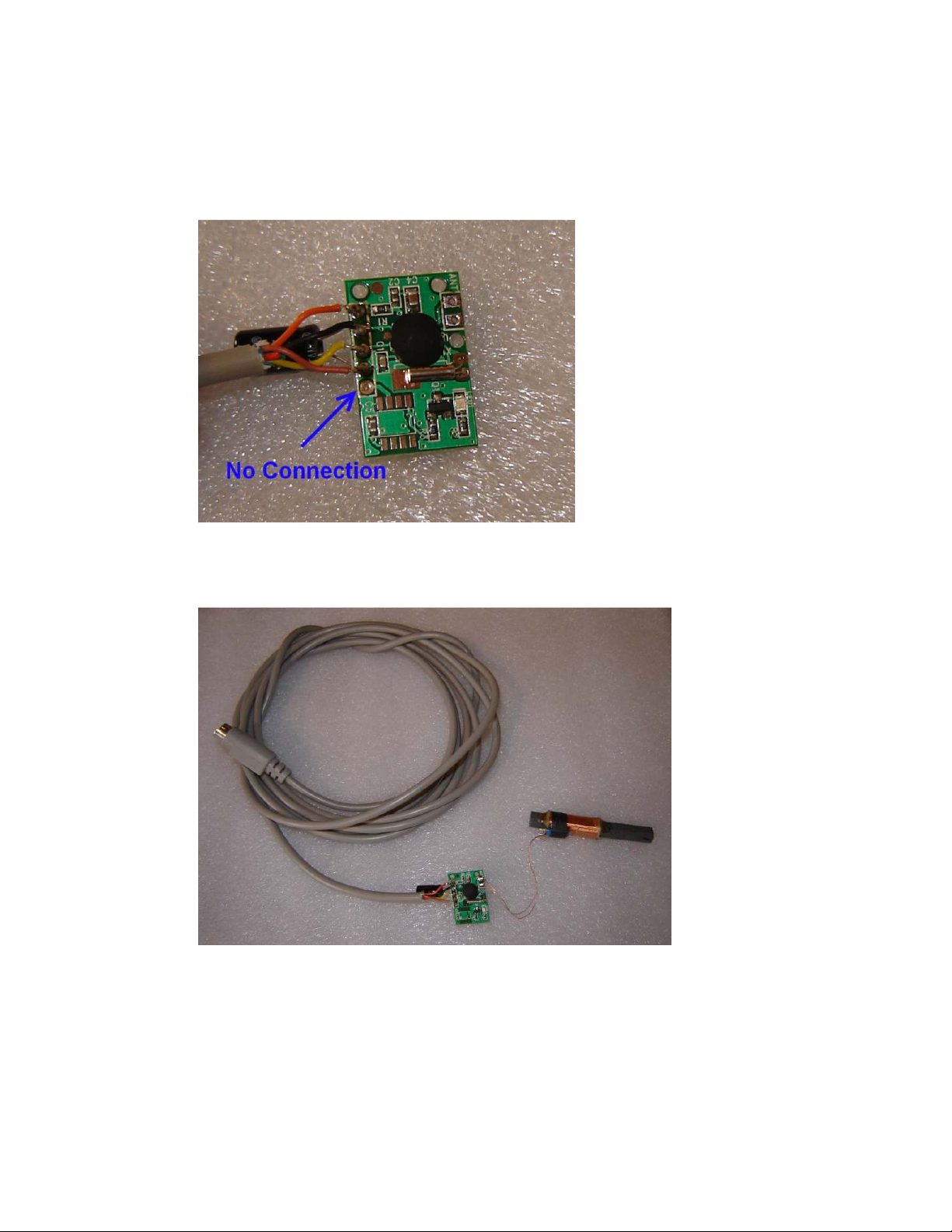
First, strip approx 15mm / 0.6” of the other grey sheath of the
cable. Identify the Black, Orange, Yellow and Brown cables and clip
off all the rest as they are not required.
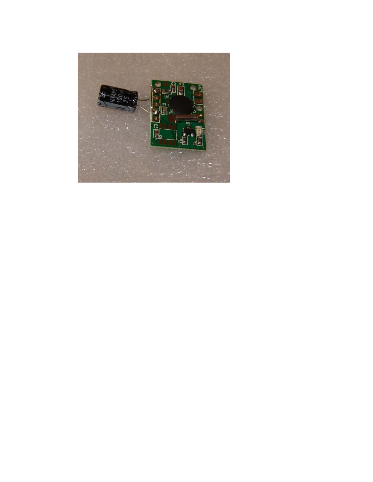
Attach a 100uF capacitor to the module as shown below to pads #1
and #4 noting the correct orientation of the negative lead of the
capacitor.
Then clip the excess capacitor leads so there is only 1-2mm
remaining.
Nixie Tube Clock ‘Frank 3’
Issue 4 (30 Sept 2011)
www.pvelectronics.co.uk
Page 29
- 29 -
Nixie Tube Clock ‘Frank 3’
Issue 4 (30 Sept 2011)
www.pvelectronics.co.uk
Page 30
- 30 -
Now connect the cables to the module as shown below. It is not
necessary to feed the cables into the holes – it is sufficient to lay
the cables over the PCB pads and solder on.
Now attach the antenna by soldering the two antenna wires to the
pads marked ‘ANT’:
The RFT Module is now ready to connect and use with the clock.
Nixie Tube Clock ‘Frank 3’
Issue 4 (30 Sept 2011)
www.pvelectronics.co.uk
Page 31
- 31 -
7.5 Mini-DIN Connector and PCB pinout.
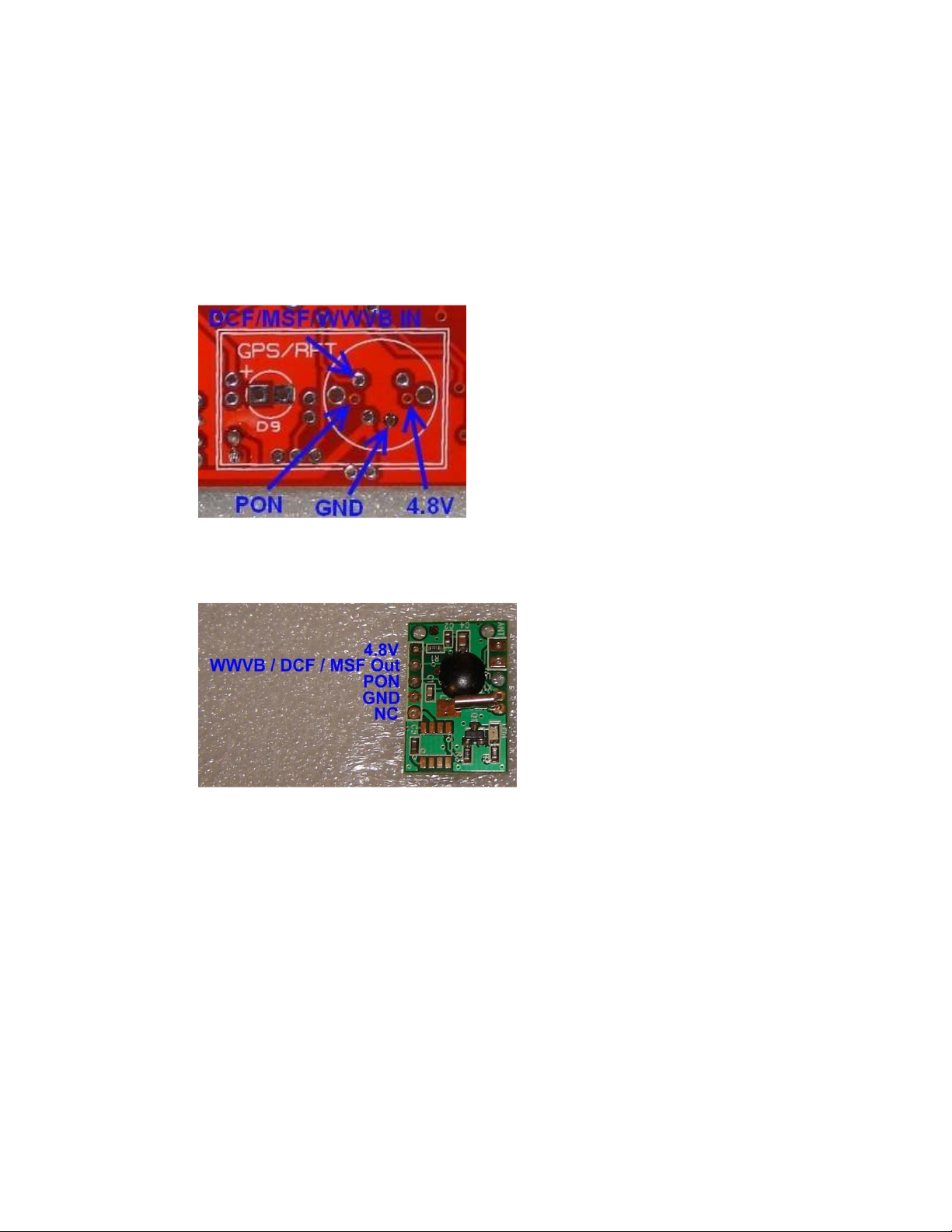
This information is needed if you are connecting a DCF / WWVB /
MSF receiver to the clock PCB directly, or without using our miniDIN extension cable. The following connections are required for
connecting a DCF / WWVB / MSF receiver module:
Bare PCB connections:
Module connections:
Note that one pad is not connected (NC).
We recommend connecting a 100uF electrolytic capacitor across
the 4.8V and GND pads as close as possible to the module.
There are no special requirements for the cable used: light duty 4way signal cable is suitable for making the connections.
Nixie Tube Clock ‘Frank 3’
Issue 4 (30 Sept 2011)
www.pvelectronics.co.uk
Page 32
- 32 -
7.6 Connecting a GPS receiver
The clock has been designed for, and tested with a Globalsat BR355 GPS receiver (available separately from PV Electronics)
It may be possible to connect other GPS receivers with the
following specification:
Power consumption max 50mA
Supply voltage 5V
Output signal levels: RS232 or TTL
Serial baud rate: 4,800 bps, 9,600 bps, 19,400 bps or 38,400 bps
Output protocol: NMEA-0183, including $GPRMC sentence
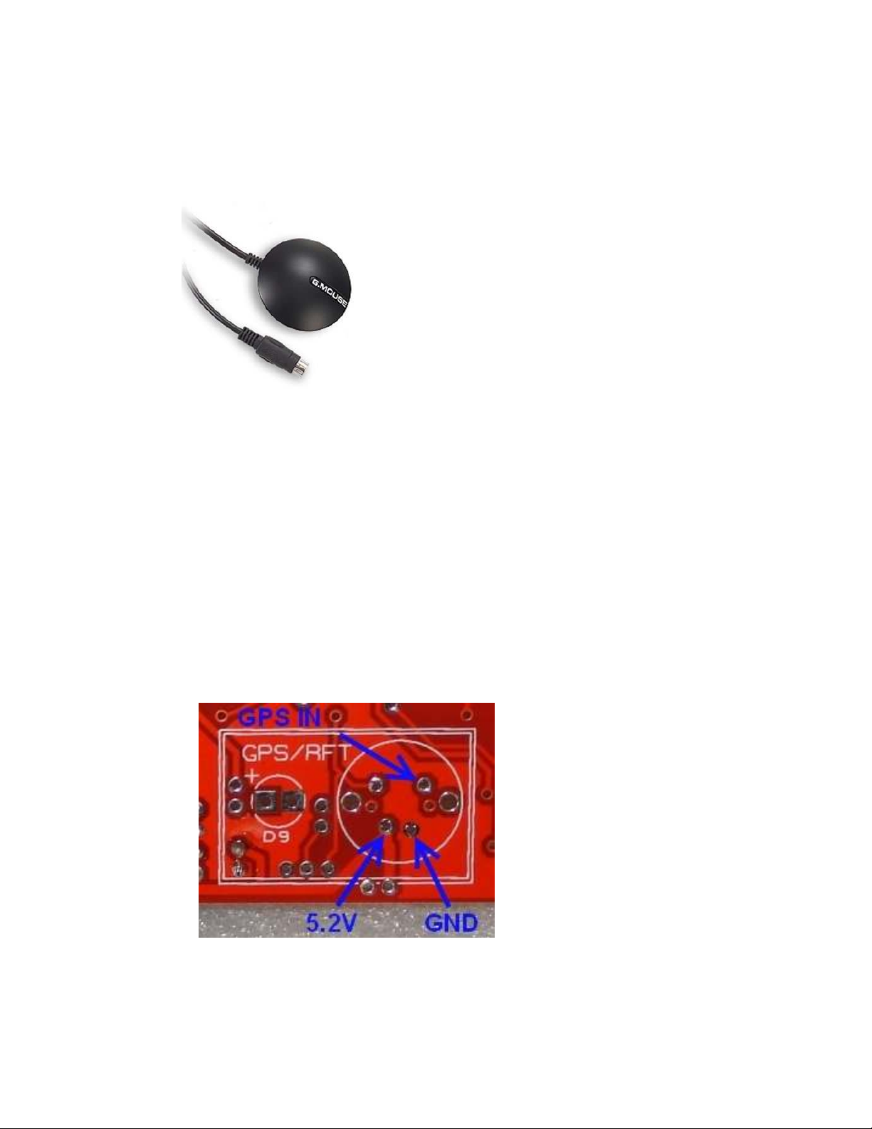
The Globalsat BR-355 receiver plugs directly into the mini-DIN
connector on the rear of the clock PCB.
To connect a different GPS receiver, the following connections are
required:
Nixie Tube Clock ‘Frank 3’
Issue 4 (30 Sept 2011)
www.pvelectronics.co.uk
Page 33
- 33 -
7.7 Function of the GPS / RFT indicator LED (D9):
• No Radio Synchronisation source installed (parameter (12) = 0)
LED is permanently off
• RFT or GPS Synchronisation enabled (parameter (12) = 1-4)
The LED will be ON if the clock has synchronised in the last two
hours; slowly flashing if the last synchronisation was between 2
hours and 24 hours ago; and off if the last synchronisation is older
than 24 hours.
• Additionally, if DCF, WWVB or MSF mode is selected, the indicator
will flash rapidly whilst the clock is actually receiving and
processing a valid time frame.
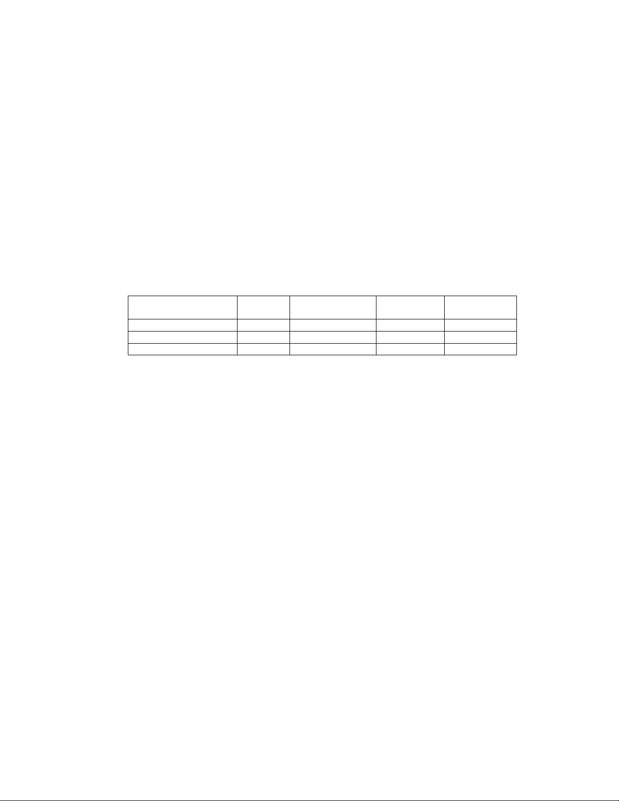
The function of the RFT indicator LED may be summarised in the
table below:
Radio Time
Source
None Off Off Off DCF / WWVB / MSF On Slow Flash Off Fast Flash
GPS On Slow Flash Off -
Sync <
2 Hrs
Sync >2 Hrs
Sync < 24 Hrs
Sync > 24
Hrs
Aquiring
RFT Frame
Nixie Tube Clock ‘Frank 3’
Issue 4 (30 Sept 2011)
www.pvelectronics.co.uk
Page 34
- 34 -
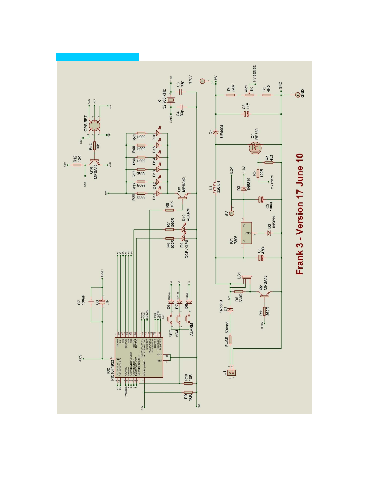
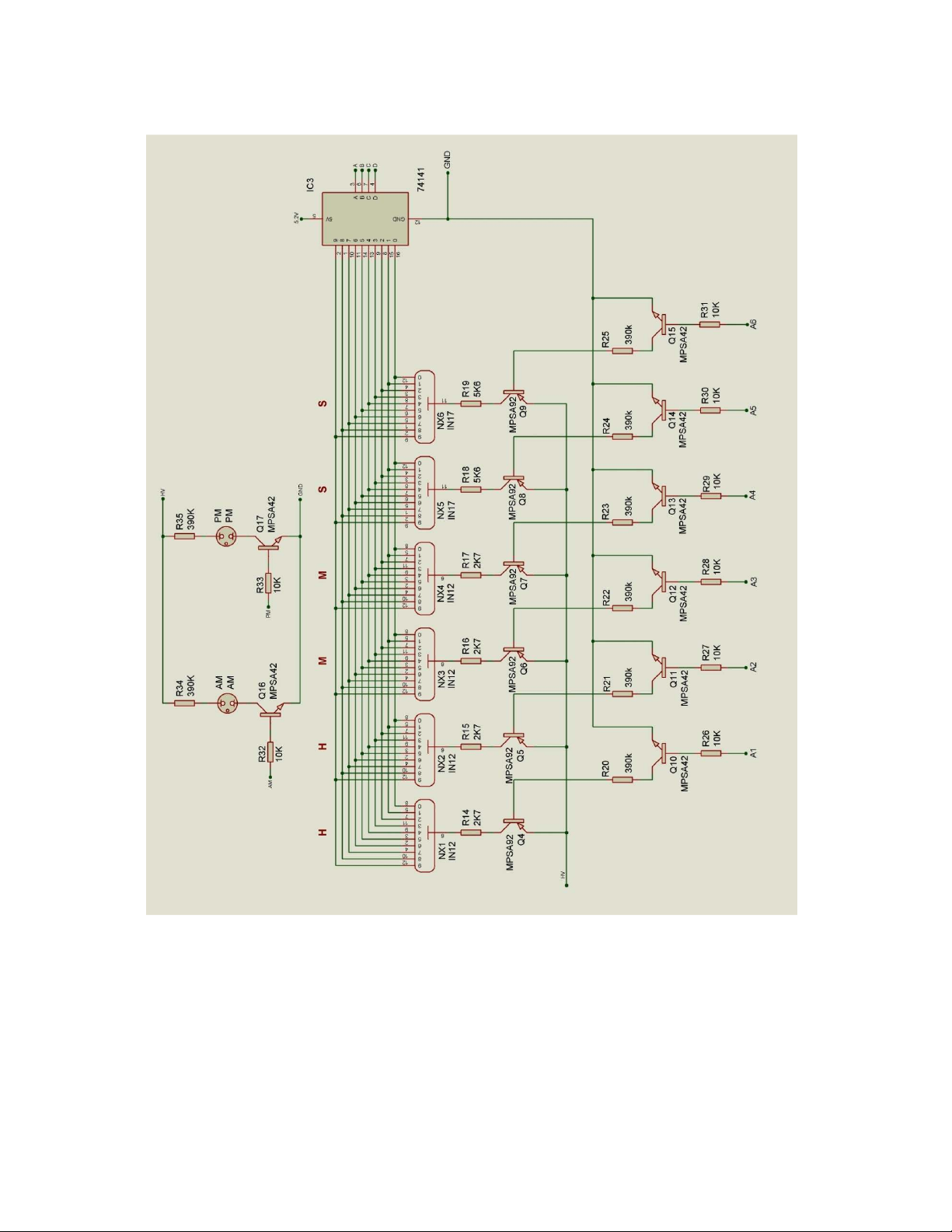
8. CIRCUIT DIAGRAM
Nixie Tube Clock ‘Frank 3’
Issue 4 (30 Sept 2011)
www.pvelectronics.co.uk
Page 35
- 35 -
Nixie Tube Clock ‘Frank 3’
Issue 4 (30 Sept 2011)
www.pvelectronics.co.uk
 Loading...