

NIKO-SEM N6200M5G, N6200M5G-1.2, N6200M5G-1.5, N6200M5G-1.8 Schematic [ru]
NIKO-SEM
1.5 MHz, 600mA Synchronous
Step-Down Converter
N6200
SOT-25
Lead-Free
GENERAL DESCRIPTION
N6200 is a 1.5Mhz constant frequency, slope compensated current mode PWM step-down converter. The
device integrates a main switch and a synchronous rectifier for high efficiency without an external Schottky
diode. It is ideal for powering portable equipment that runs from a single cell lithium-Ion (Li+) battery. The
N6200 can supply 600mA of load current from a 2.5V to 5.5V input voltage. The output voltage can be
regulated as low as 0.6V. The N6200 can also run at 100% duty cycle for low dropout operation, extending
battery life in portable system. Idle mode operation at light loads provides very low output ripple voltage for
noise sensitive applications.
The N6200 is offered in a low profile (1mm) 5-pin, thin SOT package, and is available in an adjustable
version and fixed output voltage of 1.2V, 1.5V and 1.8V.
APPLICATIONS
‧ Cellular and Smart Phones
‧ Microprocessors and DSP Core Supplies
‧ Wireless and DSL Modems
‧ PDAs
FEATURES
‧ High Efficiency: Up to 92%
‧ 1.5Mhz Constant Switching Frequency
‧ 600mA Output Current at V
‧ Integrated Main switch and synchronous
rectifier. No Schottky Diode Required
‧ 2.5V to 5.5V Input Voltage Range
‧ Output Voltage as Low as 0.6V
‧ 100% Duty Cycle in Dropout
IN
= 3V
‧ MP3 Player
‧ Digital Still and Video Cameras
‧ Portable Instruments
‧ Low Quiescent Current : 300µA
Slope Compensated ‧ Current Mode Control for
Excellent Line and Load Transient Response
Short Circuit Protection‧
Thermal Fault Protection‧
‧ <1uA Shutdown Current
‧Space Saving 5-Pin SOT-25 package
1
May-8-2006
NIKO-SEM
1.5 MHz, 600mA Synchronous
Step-Down Converter
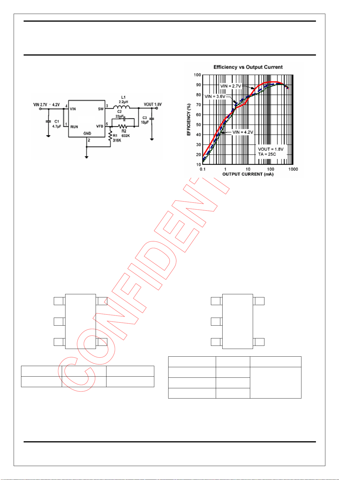
Typical Application
N6200
Figure 1 Basic Application Circuit with N6200
adjustable version, Vout = 1.8V
N6200
SOT-25
Lead-Free
Absolute Maximum Rating
Input Supply Voltage............................ -0.3V to +6V
RUN, V
SW, V
Peak SW Sink and Source Current ......................1.5A
Voltages ............................ -0.3V to VIN+0.3V
FB
Voltages...............................-0.3V to VIN+0.3V
OUT
(Note 1)
Operating Temperature Range........... ...0°C to +85°C
Junction Temperature
Storage Temperature Range ............ -40°C to +150°C
Lead Temperature (Soldering, 10s) ................+300°C
(Note2)
............................+125°C
Package/Order Information
Adjustable Output Version: Fixed Output Versions:
Run
GND
SW
Part Number Top Mark Temp range
N6200M5G A1XY
(note4)
V
VIN
FB
0°C to +85°C
Run
GND
SW
Part Number Top Mark Temp Range
N6200M5G-1.5 A2XY
N6200M5G-1.8 A3XY
N6200M5G-1.2 A4XYB
IN
V
VFB
0°C to +85°C
2
May-8-2006
NIKO-SEM
Thermal Resistance
(Note 3)
1.5 MHz, 600mA Synchronous
Step-Down Converter
:
N6200
SOT-25
Lead-Free
Package
SOT-25
θ
θ
JA
220℃/W 110℃/W
JC
Note 1: Absolute Maximum Ratings are those values beyond which the life of a device may be impaired.
Note 2: T
is calculated from the ambient temperature TA and power dissipation PD according to the
J
following formula:
TJ = T
+ PD x θJA
A
Note 3: Thermal Resistance is specified with approximately 1 square of 1 oz copper.
Note 4: XY = Manufacturing Date Code
Electrical Characteristics
(Note 5)
:
(VIN =V
= 3.6V, TA = 25°C, Test Circuit Figure 1, unless otherwise noted.)
RUN
Parameter Conditions MIN TYP MAX unit
Input Voltage Range 2.5 5.5 V
Input DC Supply Current
Active Mode
Shutdown Mode
V
= 0.5V
FB
V
= 0V, VIN = 4.2V
FB
270
0.08
400
1.0
µA
µA
TA = +25°C 0.5880 0.6000 0.6120 V Regulated Feedback Voltage
= 0°C T≦A 85°C≦ 0.5865 0.6000 0.6135 V
T
A
VFB Input Bias Current VFB = 0.65V ±30 nA
Reference Voltage Line
VIN = 2.5V to 5.5V, V
OUT
= V
(R2=0)
FB
0.11 0.40 %/V
Regulation
Regulated Output Voltage
APS1006ET5-1.2, 0°C T≦A 85°C≦ 1.164 1.200 1.236 V
APS1006ET5-1.5, 0°C T≦A 85°C≦ 1.455 1.500 1.545 V
APS1006ET5-1.8, 0°C T≦
Output Voltage Line Regulation VIN = 2.5V to 5.5V, I
OUT
85°C≦ 1.746 1.800 1.854 V
A
= 10mA
0.40 %/V
0.11
Output Voltage Load Regulation I
from 0 to 600mA
OUT
0.0015
%/mA
Maximum Output Current VIN = 3.0V 600 mA
Oscillator Frequency VFB = 0.6V or V
R
R
of P-CH MOSFET ISW = 300mA 0.30 0.50 .Ω
DS(ON)
of N-CH MOSFET ISW = -300mA 0.20 0.45 Ω
DS(ON)
Peak Inductor Current VIN = 3V, VFB = 0.5V or V
= 100% 1.2 1.5 1.8 MHz
OUT
= 90% 1.20 A
OUT
3
May-8-2006
NIKO-SEM
1.5 MHz, 600mA Synchronous
Step-Down Converter
Duty Cycle < 35%
N6200
SOT-25
Lead-Free
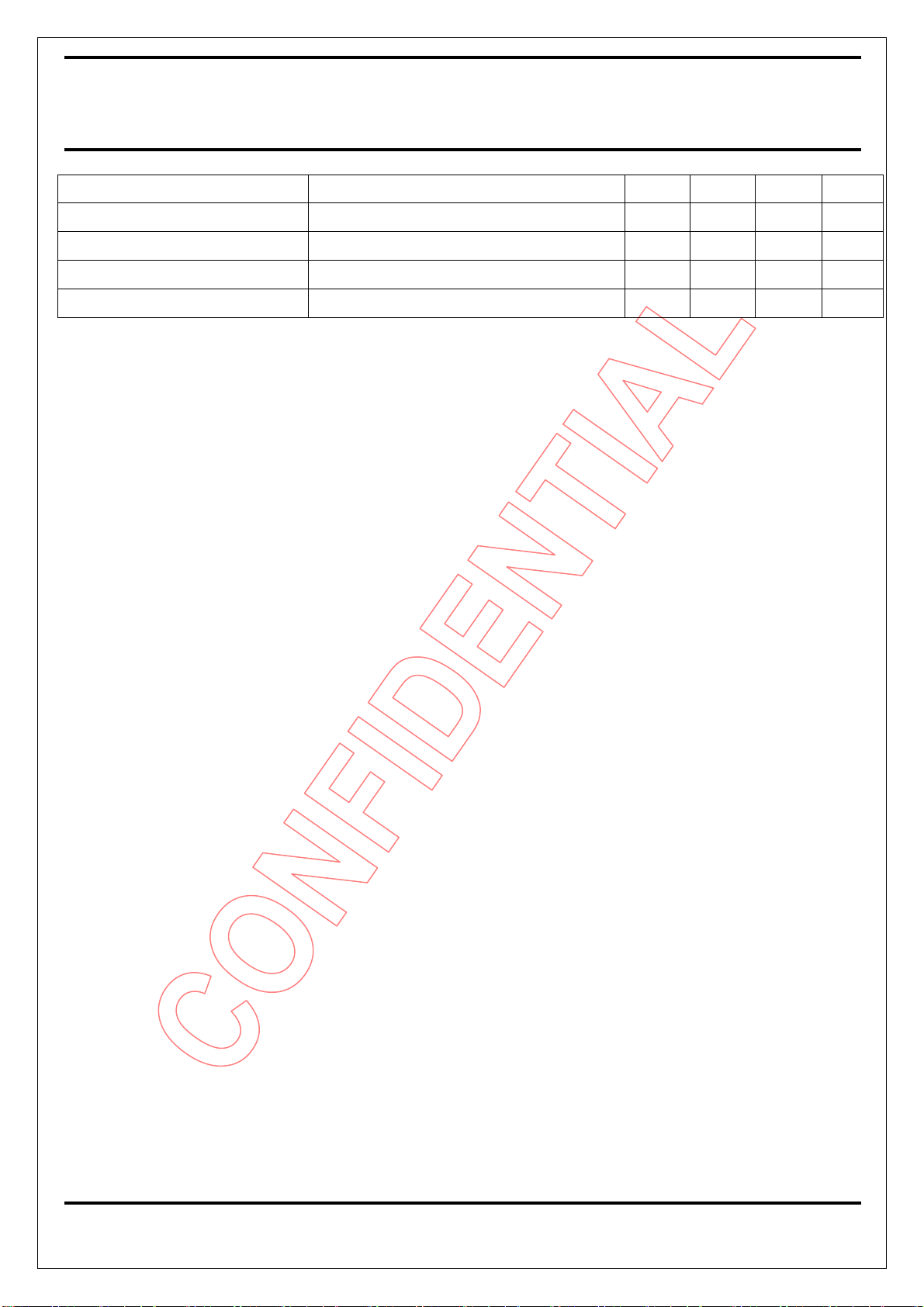
SW Leakage V
Output over voltage lockout ∆V
=0V, VSW = 0V or 5V, VIN = 5V ±0.01 ±1 µA
RUN
OVL
= V
- VFB 60 mV
OVL
RUN Threshold 0°C T≦A 85°C≦ 0.3 0.45 1.30 V
RUN Leakage Current ±0.1 ±1 µA
Note 5: 100% production test at +25°C. Specifications over the temperature range are guaranteed by
design and characterization.
4
May-8-2006
NIKO-SEM
1.5 MHz, 600mA Synchronous
Step-Down Converter
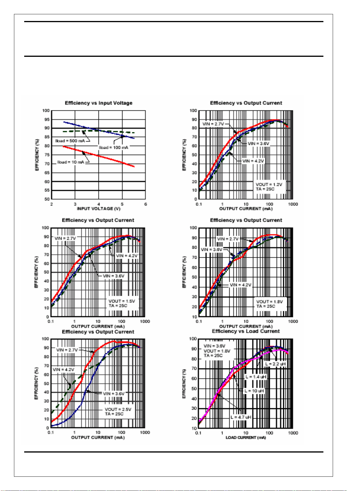
Typical Performance Characteristics
(Test Figure 1 above unless otherwise specified)
N6200
SOT-25
Lead-Free
5
May-8-2006
 Loading...