

Page 1
VAA31001-R.3651.A
作成承認印 配布許可印
VAA31001
REPAIR MANUAL
Printed in Japan February 2005
Copyright c 2005 by Nikon Corporation.
All Rights Reserved.
無断転載を禁ず
!!
Page 2

VAA31001-R.3651.A
CONTENTS
SPECIFICATIONS ・・・・・・・・・・・・・・・・・・・・・・・・・・・・・・・・・・・・・・・・・・・・・・・・・・・・・・・・・・・・・・・・・・・・・・・・・ M1-M2
Disassembly
WARNING・・・・・・・・・・・・・・・・・・・・・・・・・・・・・・・・・・・・・・・・・・・・・・・・・・・・・・・・・・・・・・・・・・・・・・・・・・・・・・・・・・ D1
REAR COVER・・・・・・・・・・・・・・・・・・・・・・・・・・・・・・・・・・・・・・・・・・・・・・・・・・・・・・・・・・・・・・・・・・・・・・・・・・・・・・・ D2
DISASSEMBLY OF REAR COVER ・・・・・・・・・・・・・・・・・・・・・・・・・・・・・・・・・・・・・・・・・・・・・・・・・・・・・・・・・・・・・ D3
Discharging of main condenser ・・・・・・・・・・・・・・・・・・・・・・・・・・・・・・・・・・・・・・・・・・・・・・・・・・・・・・・・・・・・・・・・・・ D4
FRONT COVER ・・・・・・・・・・・・・・・・・・・・・・・・・・・・・・・・・・・・・・・・・・・・・・・・・・・・・・・・・・・・・・・・・・・・・・・・・・・・・ D5
DISASSEMBLY OF FRONT COVER ・・・・・・・・・・・・・・・・・・・・・・・・・・・・・・・・・・・・・・・・・・・・・・・・・・・・・・ D6ーD7
TRIPOD SOCKET・・・・・・・・・・・・・・・・・・・・・・・・・・・・・・・・・・・・・・・・・・・・・・・・・・・・・・・・・・・・・・・・・・・・・・・・・・・・ D8
LCD ・・・・・・・・・・・・・・・・・・・・・・・・・・・・・・・・・・・・・・・・・・・・・・・・・・・・・・・・・・・・・・・・・・・・・・・・・・・・・・・・・・・・・・・ D8
SPEAKER HOLDER・・・・・・・・・・・・・・・・・・・・・・・・・・・・・・・・・・・・・・・・・・・・・・・・・・・・・・・・・・・・・・・・・・・・・・・・・・ D8
MICROPHONE ・・・・・・・・・・・・・・・・・・・・・・・・・・・・・・・・・・・・・・・・・・・・・・・・・・・・・・・・・・・・・・・・・・・・・・・・・・・・・・D9
MONITOR HOLDER ・・・・・・・・・・・・・・・・・・・・・・・・・・・・・・・・・・・・・・・・・・・・・・・・・・・・・・・・・・・・・・・・・・・・・・・・・D9
SB UNIT ・・・・・・・・・・・・・・・・・・・・・・・・・・・・・・・・・・・・・・・・・・・・・・・・・・・・・・・・・・・・・・・・・・・・・・・・・・・・・・・・・ D10
WIRE HOLDER ・・・・・・・・・・・・・・・・・・・・・・・・・・・・・・・・・・・・・・・・・・・・・・・・・・・・・・・・・・・・・・・・・・・・・・・・・・・ D11
TB-1 PCB・・・・・・・・・・・・・・・・・・・・・・・・・・・・・・・・・・・・・・・・・・・・・・・・・・・・・・・・・・・・・・・・・・・・・・・・・・・・・・・・・ D11
CONDENSER HOLDER ・・・・・・・・・・・・・・・・・・・・・・・・・・・・・・・・・・・・・・・・・・・・・・・・・・・・・・・・・・・・・・・・・・・・ D11
LENS UNIT ・・・・・・・・・・・・・・・・・・・・・・・・・・・・・・・・・・・・・・・・・・・・・・・・・・・・・・・・・・・・・・・・・・・・・・・・・・・・・・・D12
Points to notice when disassembling / (re)assembling Lens unit・・・・・・・・・・・・・・・・・・・・・・・・・・・・・・・・・・・・・・・ D13
Tools required for FFD inspection and adjustment ・・・・・・・・・・・・・・・・・・・・・・・・・・・・・・・・・・・・・・・・・・・・・・・ D13
FINDER UNIT・・・・・・・・・・・・・・・・・・・・・・・・・・・・・・・・・・・・・・・・・・・・・・・・・・・・・・・・・・・・・・・・・・・・・・・・・・・・・ D14
ZOOM MOTOR UNIT ・・・・・・・・・・・・・・・・・・・・・・・・・・・・・・・・・・・・・・・・・・・・・・・・・・・・・・・・・・・・・・・・・・・・・・D14
DISASSEMBLY OF ZOOM MOTOR UNIT ・・・・・・・・・・・・・・・・・・・・・・・・・・・・・・・・・・・・・・・・・・・・・・・・・・・・・ D15
CCD FRAME・・・・・・・・・・・・・・・・・・・・・・・・・・・・・・・・・・・・・・・・・・・・・・・・・・・・・・・・・・・・・・・・・・・・・・・・・・・・・・ D16
BARRIER UNIT ・・・・・・・・・・・・・・・・・・・・・・・・・・・・・・・・・・・・・・・・・・・・・・・・・・・・・・・・・・・・・・・・・・・・・・・・・・・D17
FIXED BARREL ・・・・・・・・・・・・・・・・・・・・・・・・・・・・・・・・・・・・・・・・・・・・・・・・・・・・・・・・・・・・・・・・・・・・・・・・・・・D18
DISASSEMBLY OF FIXED BARREL・・・・・・・・・・・・・・・・・・・・・・・・・・・・・・・・・・・・・・・・・・・・・・・・・・・・・・・・・・ D18
2ND LENS GROUP UNIT ・・・・・・・・・・・・・・・・・・・・・・・・・・・・・・・・・・・・・・・・・・・・・・・・・・・・・・・・・・・・・・・・・・・D19
SHUTTER ・・・・・・・・・・・・・・・・・・・・・・・・・・・・・・・・・・・・・・・・・・・・・・・・・・・・・・・・・・・・・・・・・・・・・・・・・・・・・・・・ D19
STRAIGHT BARREL ・・・・・・・・・・・・・・・・・・・・・・・・・・・・・・・・・・・・・・・・・・・・・・・・・・・・・・・・・・・・・・・・・・・・・・・D19
KEY BARREL ・TURN BARREL ・・・・・・・・・・・・・・・・・・・・・・・・・・・・・・・・・・・・・・・・・・・・・・・・・・・・・・・・・・・・・ D20
1ST LENS GROUP UNIT ・・・・・・・・・・・・・・・・・・・・・・・・・・・・・・・・・・・・・・・・・・・・・・・・・・・・・・・・・・・・・・・・・・・・ D20
ASSEMBLY
1ST LENS GROUP UNIT ・・・・・・・・・・・・・・・・・・・・・・・・・・・・・・・・・・・・・・・・・・・・・・・・・・・・・・・・・・・・・・・・・・・・・・ A1
KEY BARREL ・TURN BARREL ・・・・・・・・・・・・・・・・・・・・・・・・・・・・・・・・・・・・・・・・・・・・・・・・・・・・・・・・・・・・・・・ A1
STRAIGHT BARREL ・・・・・・・・・・・・・・・・・・・・・・・・・・・・・・・・・・・・・・・・・・・・・・・・・・・・・・・・・・・・・・・・・・・・・・・・・A2
SHUTTER ・・・・・・・・・・・・・・・・・・・・・・・・・・・・・・・・・・・・・・・・・・・・・・・・・・・・・・・・・・・・・・・・・・・・・・・・・・・・・・・・・・ A2
- E5600 -
Page 3

VAA31001-R.3651.A
2ND LENS GROUP UNIT ・・・・・・・・・・・・・・・・・・・・・・・・・・・・・・・・・・・・・・・・・・・・・・・・・・・・・・・・・・・・・・・・・・・・・A3
ASSEMBLY OF FIXED BARREL ・・・・・・・・・・・・・・・・・・・・・・・・・・・・・・・・・・・・・・・・・・・・・・・・・・・・・・・・・・・・・・・A3
FIXED BARREL ・・・・・・・・・・・・・・・・・・・・・・・・・・・・・・・・・・・・・・・・・・・・・・・・・・・・・・・・・・・・・・・・・・・・・・・・・・・・・A4
CCD FRAME・・・・・・・・・・・・・・・・・・・・・・・・・・・・・・・・・・・・・・・・・・・・・・・・・・・・・・・・・・・・・・・・・・・・・・・・・・・・・・・・ A5
ASSEMBLY OF ZOOM MOTOR UNIT ・・・・・・・・・・・・・・・・・・・・・・・・・・・・・・・・・・・・・・・・・・・・・・・・・・・・・・・・・・A6
ZOOM MOTOR UNIT ・・・・・・・・・・・・・・・・・・・・・・・・・・・・・・・・・・・・・・・・・・・・・・・・・・・・・・・・・・・・・・・・・・・・・・・・A7
FFD Inspection and adjustment (*FFD:Flange Focal Distance) ・・・・・・・・・・・・・・・・・・・・・・・・・・・・・・・・・・・・・・・・・ A8
Preparation ・・・・・・・・・・・・・・・・・・・・・・・・・・・・・・・・・・・・・・・・・・・・・・・・・・・・・・・・・・・・・・・・・・・・・・・・・・・・・・・・A8
FFD inspection and adjustment ・・・・・・・・・・・・・・・・・・・・・・・・・・・・・・・・・・・・・・・・・・・・・・・・・・・・・・・・ A8-A10
FFD adjustment ・・・・・・・・・・・・・・・・・・・・・・・・・・・・・・・・・・・・・・・・・・・・・・・・・・・・・・・・・・・・・・・・・・・・・・・・・・A10
BARRIER UNIT ・・・・・・・・・・・・・・・・・・・・・・・・・・・・・・・・・・・・・・・・・・・・・・・・・・・・・・・・・・・・・・・・・・・A11-A12
Operation inspection ・・・・・・・・・・・・・・・・・・・・・・・・・・・・・・・・・・・・・・・・・・・・・・・・・・・・・・・・・・・・・・・・・・・・・・・・ A12
FINDER UNIT・・・・・・・・・・・・・・・・・・・・・・・・・・・・・・・・・・・・・・・・・・・・・・・・・・・・・・・・・・・・・・・・・・・・・・・・・・・・・ A12
Resolution inspection ・・・・・・・・・・・・・・・・・・・・・・・・・・・・・・・・・・・・・・・・・・・・・・・・・・・・・・・・・・・・・・・・・・・・・・・・ A13
LENS UNIT ・・・・・・・・・・・・・・・・・・・・・・・・・・・・・・・・・・・・・・・・・・・・・・・・・・・・・・・・・・・・・・・・・・・・・・・・・・・・・・・A14
CONDENSER HOLDER ・・・・・・・・・・・・・・・・・・・・・・・・・・・・・・・・・・・・・・・・・・・・・・・・・・・・・・・・・・・・・・・・・・・・ A15
TB-1 PCB・・・・・・・・・・・・・・・・・・・・・・・・・・・・・・・・・・・・・・・・・・・・・・・・・・・・・・・・・・・・・・・・・・・・・・・・・・・・・・・・・ A15
WIRE HOLDER ・・・・・・・・・・・・・・・・・・・・・・・・・・・・・・・・・・・・・・・・・・・・・・・・・・・・・・・・・・・・・・・・・・・・・・・・・・・ A16
SB UNIT ・・・・・・・・・・・・・・・・・・・・・・・・・・・・・・・・・・・・・・・・・・・・・・・・・・・・・・・・・・・・・・・・・・・・・・・・・ A16-A18
MONITOR HOLDER ・・・・・・・・・・・・・・・・・・・・・・・・・・・・・・・・・・・・・・・・・・・・・・・・・・・・・・・・・・・・・・・・・・・・・・・A18
MICROPHONE ・・・・・・・・・・・・・・・・・・・・・・・・・・・・・・・・・・・・・・・・・・・・・・・・・・・・・・・・・・・・・・・・・・・・・・・・・・・・A19
SPEAKER HOLDER・・・・・・・・・・・・・・・・・・・・・・・・・・・・・・・・・・・・・・・・・・・・・・・・・・・・・・・・・・・・・・・・・・・・・・・・ A20
LCD ・・・・・・・・・・・・・・・・・・・・・・・・・・・・・・・・・・・・・・・・・・・・・・・・・・・・・・・・・・・・・・・・・・・・・・・・・・・・・・・・・・・・・ A20
TRIPOD SOCKET・・・・・・・・・・・・・・・・・・・・・・・・・・・・・・・・・・・・・・・・・・・・・・・・・・・・・・・・・・・・・・・・・・・・・・・・・・ A21
ASSEMBLY OF FRONT COVER・・・・・・・・・・・・・・・・・・・・・・・・・・・・・・・・・・・・・・・・・・・・・・・・・・・・・・ A21-A22
FRONT COVER ・・・・・・・・・・・・・・・・・・・・・・・・・・・・・・・・・・・・・・・・・・・・・・・・・・・・・・・・・・・・・・・・・・・・・・・・・・・ A23
ASSEMBLY OF REAR COVER・・・・・・・・・・・・・・・・・・・・・・・・・・・・・・・・・・・・・・・・・・・・・・・・・・・・・・・・・・・・・・・ A23
REAR COVER・・・・・・・・・・・・・・・・・・・・・・・・・・・・・・・・・・・・・・・・・・・・・・・・・・・・・・・・・・・・・・・・・・・・・・・・・・・・・ A24
ADJUSTMENT ・・・・・・・・・・・・・・・・・・・・・・・・・・・・・・・・・・・・・・・・・・・・・・・・・・・・・・・・・・・・・・・・・・・・・・・ A25-A35
DISCRIPTION OF CIRCUIT・・・・・・・・・・・・・・・・・・・・・・・・・・・・・・・・・・・・・・・・・・・・・・・・・・・・・・・・・・・・・・・・・ E1-E8
ELECTRICITY
OVERALL WIRING ・・・・・・・・・・・・・・・・・・・・・・・・・・・・・・・・・・・・・・・・・・・・・・・・・・・・・・・・・・・・・・・・・・・・・・・・・・E9
CP1(DMA)CIRCUIT DIAGRAM・・・・・・・・・・・・・・・・・・・・・・・・・・・・・・・・・・・・・・・・・・・・・・・・・・・・・・・・・・・・・・ E10
CP1(SYA) CIRCUIT DIAGRAM ・・・・・・・・・・・・・・・・・・・・・・・・・・・・・・・・・・・・・・・・・・・・・・・・・・・・・・・・・・・・・・ E11
CP1(CAA) CIRCUIT DIAGRAM・・・・・・・・・・・・・・・・・・・・・・・・・・・・・・・・・・・・・・・・・・・・・・・・・・・・・・・・・・・・・・ E12
CP1(PWA) CIRCUIT DIAGRAM・・・・・・・・・・・・・・・・・・・・・・・・・・・・・・・・・・・・・・・・・・・・・・・・・・・・・・・・・・・・・・ E13
CP1(STA) CIRCUIT DIAGRAM ・・・・・・・・・・・・・・・・・・・・・・・・・・・・・・・・・・・・・・・・・・・・・・・・・・・・・・・・・・・・・・E14
ST1 CIRCUIT DIAGRAM ・・・・・・・・・・・・・・・・・・・・・・・・・・・・・・・・・・・・・・・・・・・・・・・・・・・・・・・・・・・・・・・・・・・E15
- E5600 -
Page 4

VAA31001-R.3651.A
TB1 CIRCUIT DIAGRAM ・・・・・・・・・・・・・・・・・・・・・・・・・・・・・・・・・・・・・・・・・・・・・・・・・・・・・・・・・・・・・・・・・・・ E16
TB2 CIRCUIT DIAGRAM ・・・・・・・・・・・・・・・・・・・・・・・・・・・・・・・・・・・・・・・・・・・・・・・・・・・・・・・・・・・・・・・・・・・ E17
OVERALL BLOCK DIAGRAM・・・・・・・・・・・・・・・・・・・・・・・・・・・・・・・・・・・・・・・・・・・・・・・・・・・・・・・・・・・・・・・ E18
CCD BLOCK DIAGRAM・・・・・・・・・・・・・・・・・・・・・・・・・・・・・・・・・・・・・・・・・・・・・・・・・・・・・・・・・・・・・・・・・・・・ E19
LENS BLOCK DIAGRAM ・・・・・・・・・・・・・・・・・・・・・・・・・・・・・・・・・・・・・・・・・・・・・・・・・・・・・・・・・・・・・・・・・・・ E20
ASIC BLOCK DIAGRAM ・・・・・・・・・・・・・・・・・・・・・・・・・・・・・・・・・・・・・・・・・・・・・・・・・・・・・・・・・・・・・・・・・・・E21
SYSTEM CONTROL BLOCK DIAGRAM ・・・・・・・・・・・・・・・・・・・・・・・・・・・・・・・・・・・・・・・・・・・・・・・・・・・・・・ E22
POWER BLOCK DIAGRAM ・・・・・・・・・・・・・・・・・・・・・・・・・・・・・・・・・・・・・・・・・・・・・・・・・・・・・・・・・・・・・・・・・ E23
FUSE arrangement (CP1 PCB) ・・・・・・・・・・・・・・・・・・・・・・・・・・・・・・・・・・・・・・・・・・・・・・・・・・・・・・・・・・・・・・・・E24
INSPECTION STANDARDS・・・・・・・・・・・・・・・・・・・・・・・・・・・・・・・・・・・・・・・・・・・・・・・・・・・・・・・・・・・・・・・ R1-R10
Tool List ・・・・・・・・・・・・・・・・・・・・・・・・・・・・・・・・・・・・・・・・・・・・・・・・・・・・・・・・・・・・・・・・・・・・・・・・・・・・・・・・・ T1-T5
- E5600 -
Page 5

SPECIFICATIONS
Type E5600 digital camera
Effective pixels 5.1 million
CCD
1/2.5” high-density CCD; total pixels: 5.36 million
VAA31001-R.3651.A
Image size (pixels)
Lens
Focal length
f/-number
Construction
Digital zoom 4 × (35-mm [135] camera-format equivalent:420 mm)
Autofocus (AF)
Focus range
Focus-area selection
Viewnder
Magnification
Frame coverage
Monitor
2,592 × 1,944 (2592)
2,048 × 1,536 (2048)
1,024 × 768 (1024)
640 × 480 (640)
3 × Zoom Nikkor
F=5.7 - 17.1 mm
(35-mm [135] camera-format equivalent: 35 - 105 mm)
f/2.9 - f/4.9
Seven elements in six groups
Contrast-detect through the lens (TTL) AF
30 cm (1') - ∞ ; macro mode 4 cm/1.6” (M) - ∞
Center with ve-area selection in frame assist mode
Real-image zoom viewnder with LED indication
0.3 - 0.76 ×
Approximately 82% horizontal and 82% vertical
1.8”, 80,000-dot, amorphous silicon TFT LCD monitor
Frame coverage
(shooting mode)
Storage Media
File system
File formats
Exposure
Metering
Exposure control
Range
Shutter
Speed
Aperture
Range
Sensitivity Approximately equivalent to ISO 50
Approximately 97% horizontal and 97% vertical
Internal memory (14 MB)/SD memory cards
Compliant with Design Rule for Camera File System (DCF),
Exif 2.2, and Digital Print Order Format (DPOF)
Compressed: JPEG-baseline-compliant, Movies: QuickTime
256-segment matrix metering linked to AF area
(when frame is displayed in frame-assisted scene mode)
Programmed auto exposure with exposure compensation
(-2.0 - +2.0 EV in steps of 1/3 EV)
W: +1.1 - +17.1 EV, T: +2.6 - +18.6 EV
Mechanical and charge-coupled electronic shutter
4 - 1/3,000 s
Electronically-controlled preset aperture
Two steps (f/2.9 and f/4.9 [W])
(auto gain of two to four times) (up to equivalent of ISO 200)
Self-timer Ten-second duration
- M1・ E5600 -
Page 6

Built-in Speedlight
VAA31001-R.3651.A
Range (approx.)
Flash control
Interface USB
Video output Can be selected from NTSC and PAL
I/O terminals A/V out/digital I/O
Power sources ・Two rechargeable Nikon EN-MH1 NiMH batteries
Nu m ber of fram es tak en in
succession
Dimensions (W × H × D) 85 × 60 × 35 mm (3.3” × 2.4” × 1.3”)
Approximate weight 130 g (4.6 oz) without battery or memory card
Operating environment
W: 0.4 - 3.3 m/1'4” - 10'10”
T: 0.4 - 2.0 m/1'4” - 6'7”
Sensor ash system
・Two LR6 (AA) alkaline batteries
・Two ZR6 (AA) nickel manganese batteries
・Two FR6/L91 (AA) lithium batteries
・EH-62B AC adapter
・220 frames (alkaline batteries)
・340 frames (EN-MH1)
・600 frames (lithium batteries)
Measured at standard temperature (25 ℃ /77 °F ) with fully charged batteries based on
CIPA standard: zoom adjusted with each shot, ash used in approximately one half of
shots, image type set to Normal.
Temperature
Humidity
0 - 40 ℃ (32 - 104°F )
Less than 85% (no condensation)
- M2・ E5600 -
Page 7
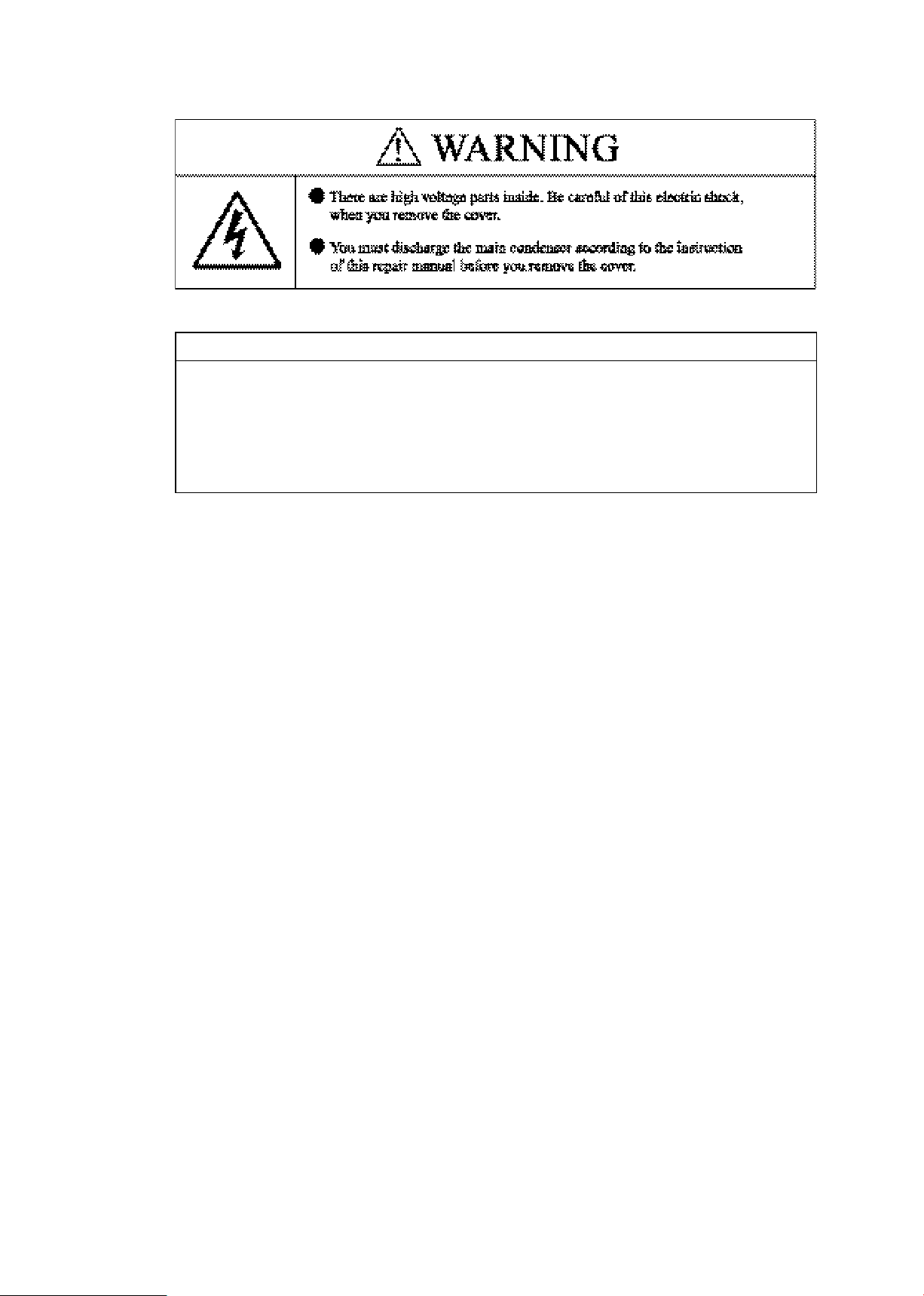
Disassembly
・ Lead-free solder is used for this product.
・ For soldering work, the special solder and soldering iron are required.
・ Do NOT mix up lead-free solder with traditional solder.
・ Use the special soldering iron respectively for lead-free solder and lead solder. They cannot
be used in common.
VAA31001-R.3651.A
Points to notice for Lead-free solder products
Note : ① Be sure to remove the SD memory card and batteries before disassembly.
② When disassembling, make sure to memorize the processing state of wires, screws to be
xed and their types, etc.
③ Because electrical parts are easily damaged by static electricity, make sure that you are
well earthed/grounded.
- D1・ E5600 -
Page 8
VAA31001-R.3651.A
- D2・ E5600 -
REAR COVER
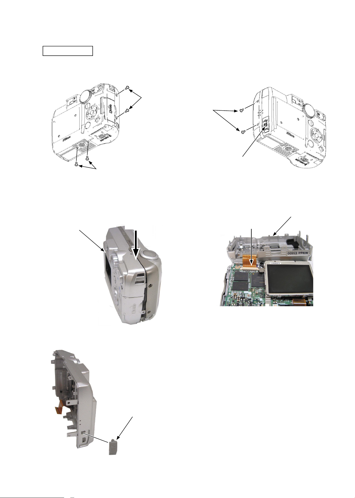
・ Remove the four screws [#102]. ・ Remove the two screws [#103].
・ Open the USB cover [#033].
・ As pushing the top side of the rear cover unit [#030]
by your nger, perform unhooking.
・ Open the rear cover unit [#030] slowly backward and
remove the FPC.
・ Remove the USB cover [#033].
Rear cover unit [#030]
FPC
Push.
Rear cover unit [#030]
Screw [#103]
USB cover [#033]
USB cover [#033]
Screw [#102]
Screw [#102]
Page 9
DISASSEMBLY OF REAR COVER
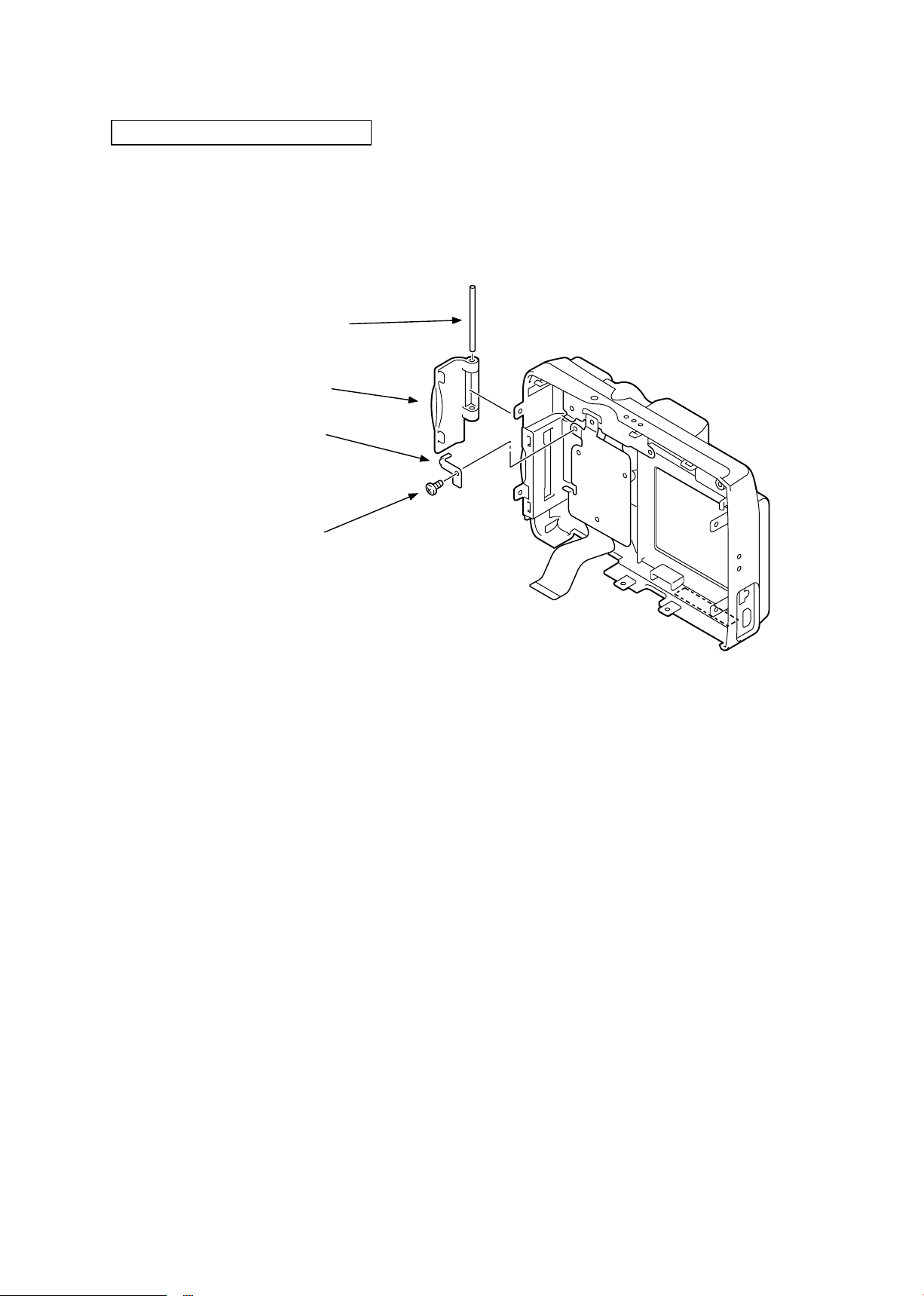
・ Remove the screw [#104].
・ Remove the earth shaft [#029].
・ Remove the cover shaft [#009].
・ Remove the SD cover [#037].
Cover shaft [#009]
SD cover [#037]
Earth shaft [#029]
VAA31001-R.3651.A
Screw [#104]
- D3・ E5600 -
Page 10
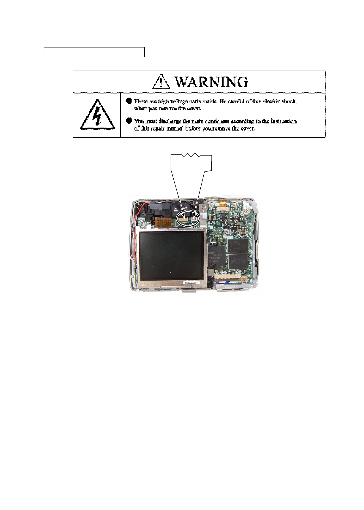
Discharging of main condenser
VAA31001-R.3651.A
2KΩ/5W
- D4・ E5600 -
Page 11
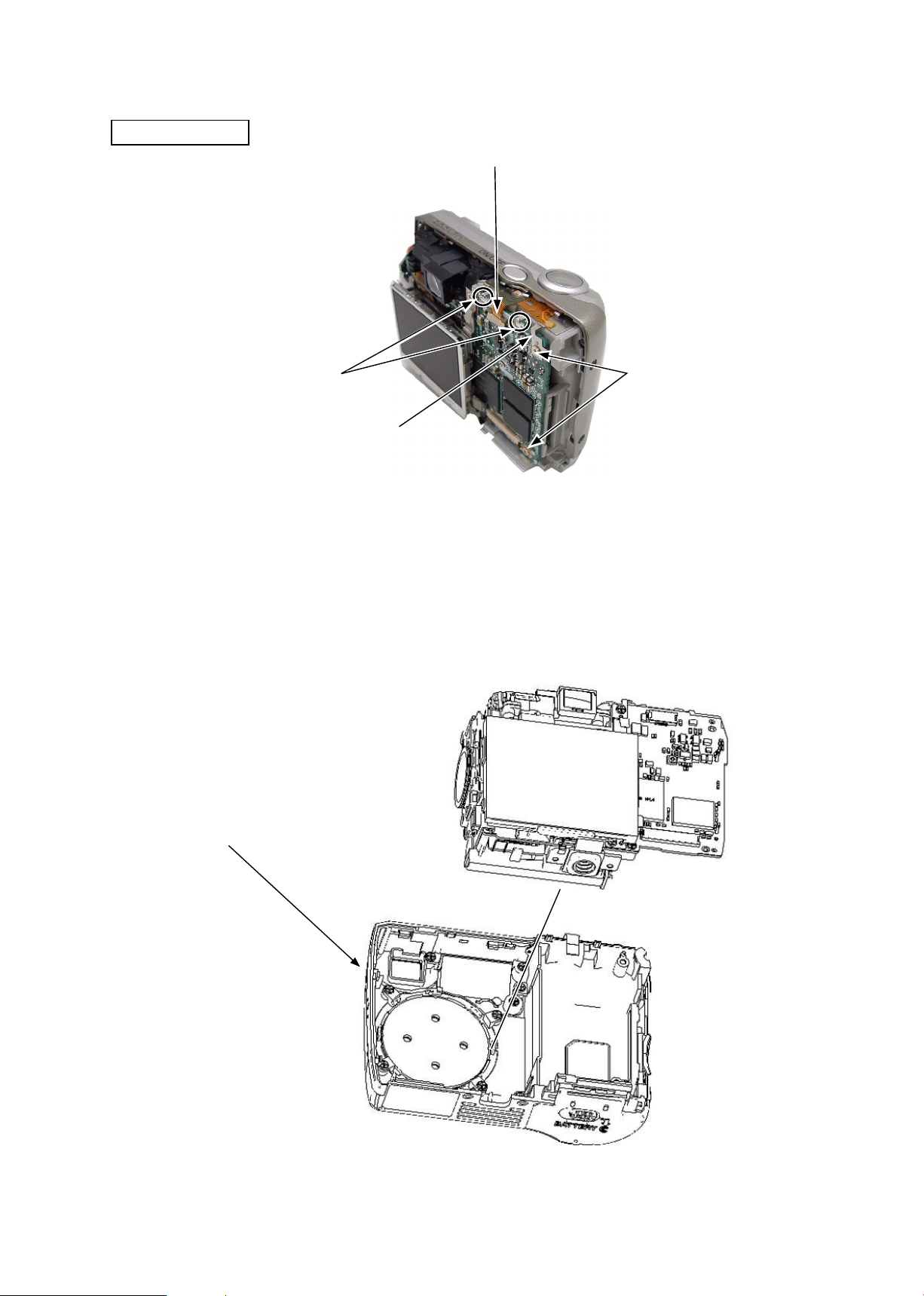
FRONT COVER
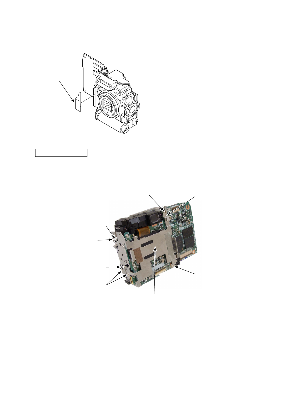
・ Remove the solder at 2 places.
・ Remove the FPC.
・ Remove the two screws [#102].
・ The earth release [#026] can be removed.
VAA31001-R.3651.A
FPC
Solder
Earth release [#026]
・ Remove the front cover [#013].
Screw [#102]
Front cover [#013]
- D5・ E5600 -
Page 12
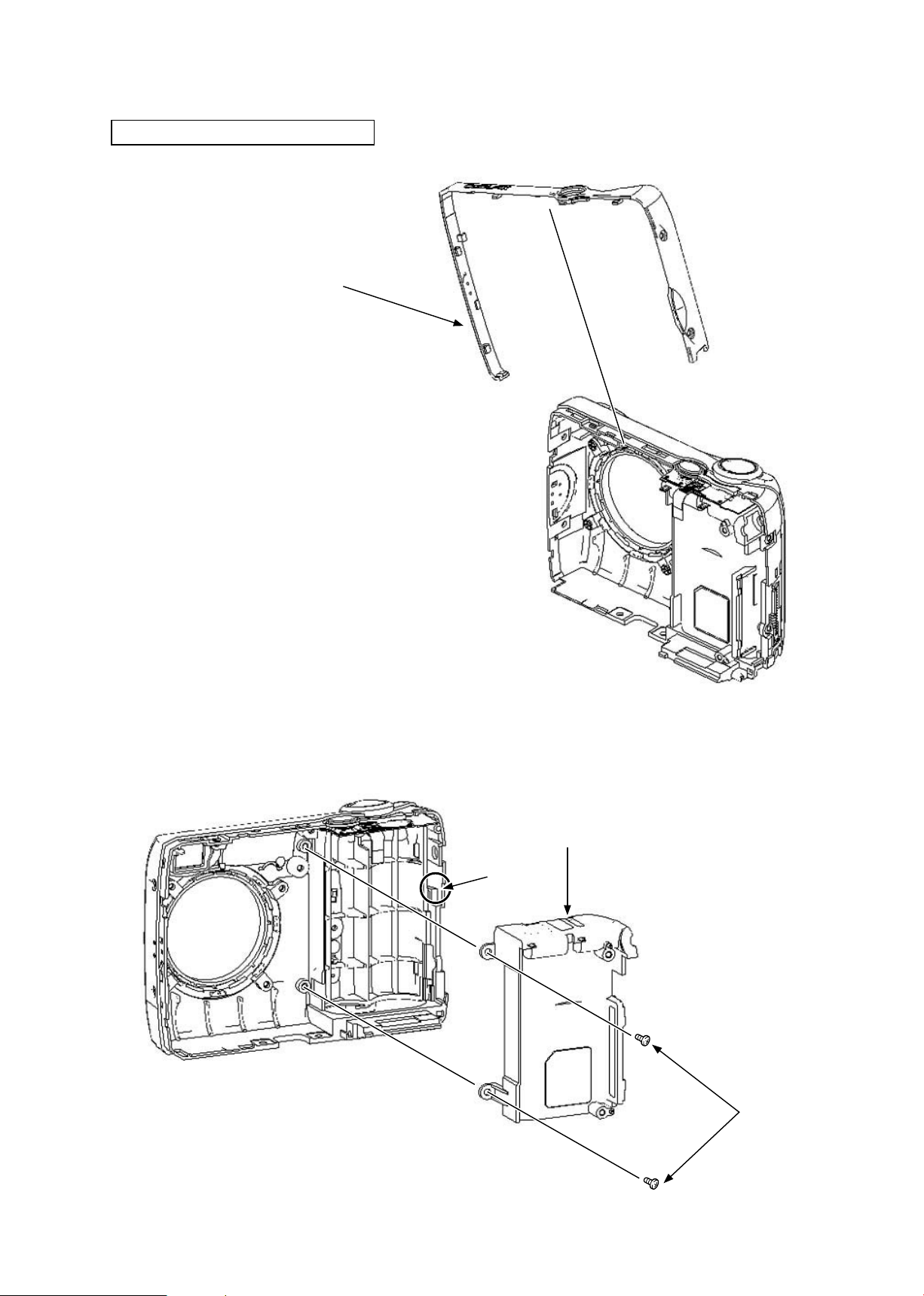
DISASSEMBLY OF FRONT COVER
・ Remove the decoration top [#021].
Decoration top [#021]
VAA31001-R.3651.A
・ Remove the two screws [#104].
・ Unhook the battery holder [#024].
Battery holder [#024]
Hook
Screw [#104]
- D6・ E5600 -
Page 13
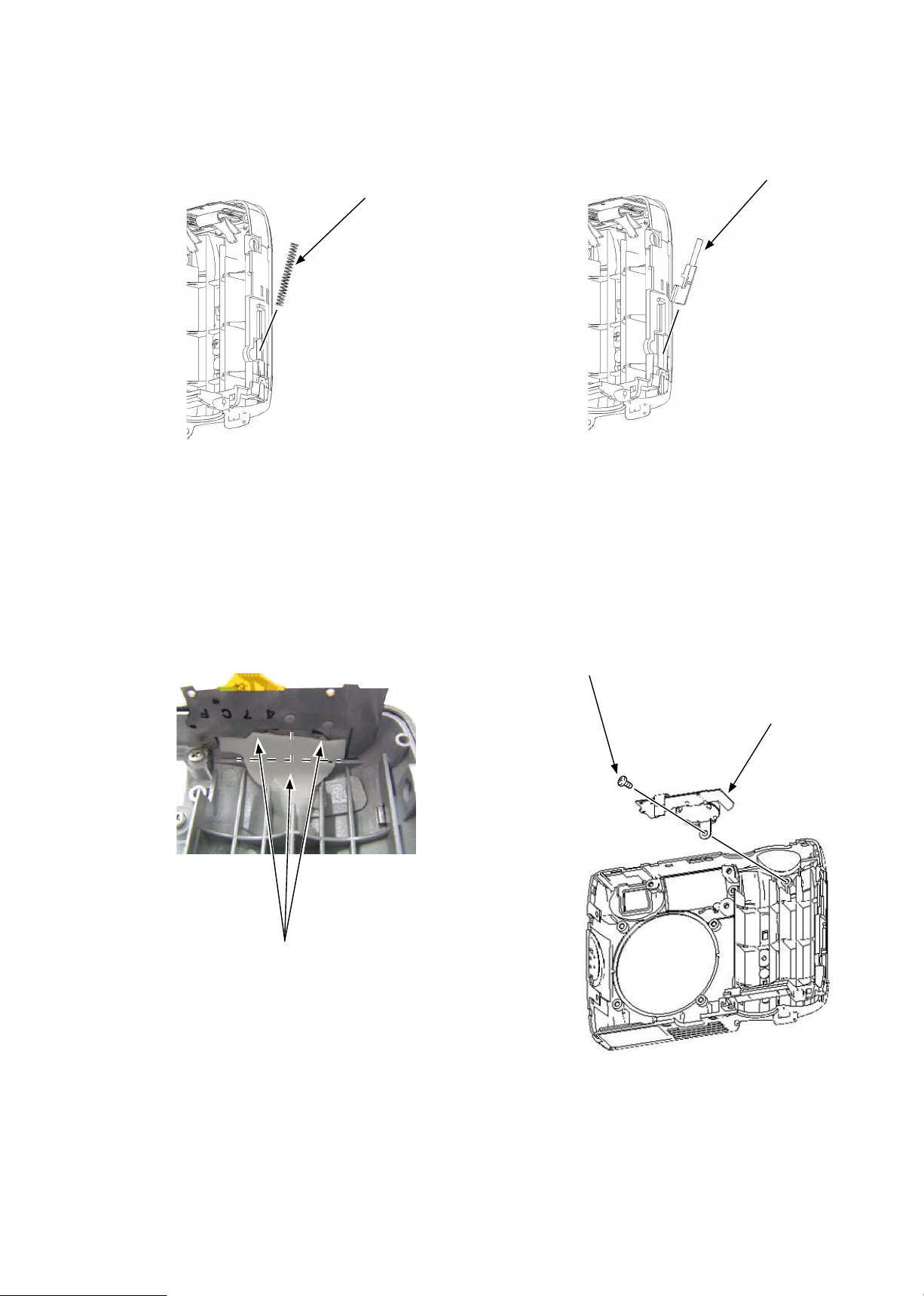
・ Remove the DC cover spring [#012]. ・ Pull out the DC cover [#011].
DC cover [#011]
DC cover spring [#012]
VAA31001-R.3651.A
・ Take off the spacer [#019] from the release button
unit.
※ In the gure below, the spacer is divided into three
pieces from the dotted line.
Spacer [#019]
・ Remove the screw [#104].
・ Remove the release button unit [#020].
Screw [#104]
Release button unit [#020]
- D7・ E5600 -
Page 14
VAA31001-R.3651.A
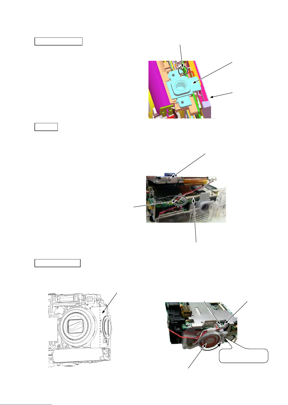
TRIPOD SOCKET
・ Perform unhooking and remove the tripod socket
[#201].
LCD
・ Lift up the LCD [#239] and unsolder the lead wires [red] and [white].
※ The LCD [#239] is adhered with the double-adhesive tape.
・ Remove the FPC.
・ Remove the LCD [#239].
Hook
Tripod socket [#201]
LCD[#239]
LCD[#239]
Lead wires [red] and [white]
FPC
SPEAKER HOLDER
・ Take off the spacer [#206]. ・ Unsolder the lead wires [red] and [white].
・ As turning counterclockwise, remove the speaker
Spacer [#206]
holder [#233].
Lead wire [red]Lead wire [white]
- D8・ E5600 -
Float this section and
remove it as turning.
Speaker holder [#233]
Page 15
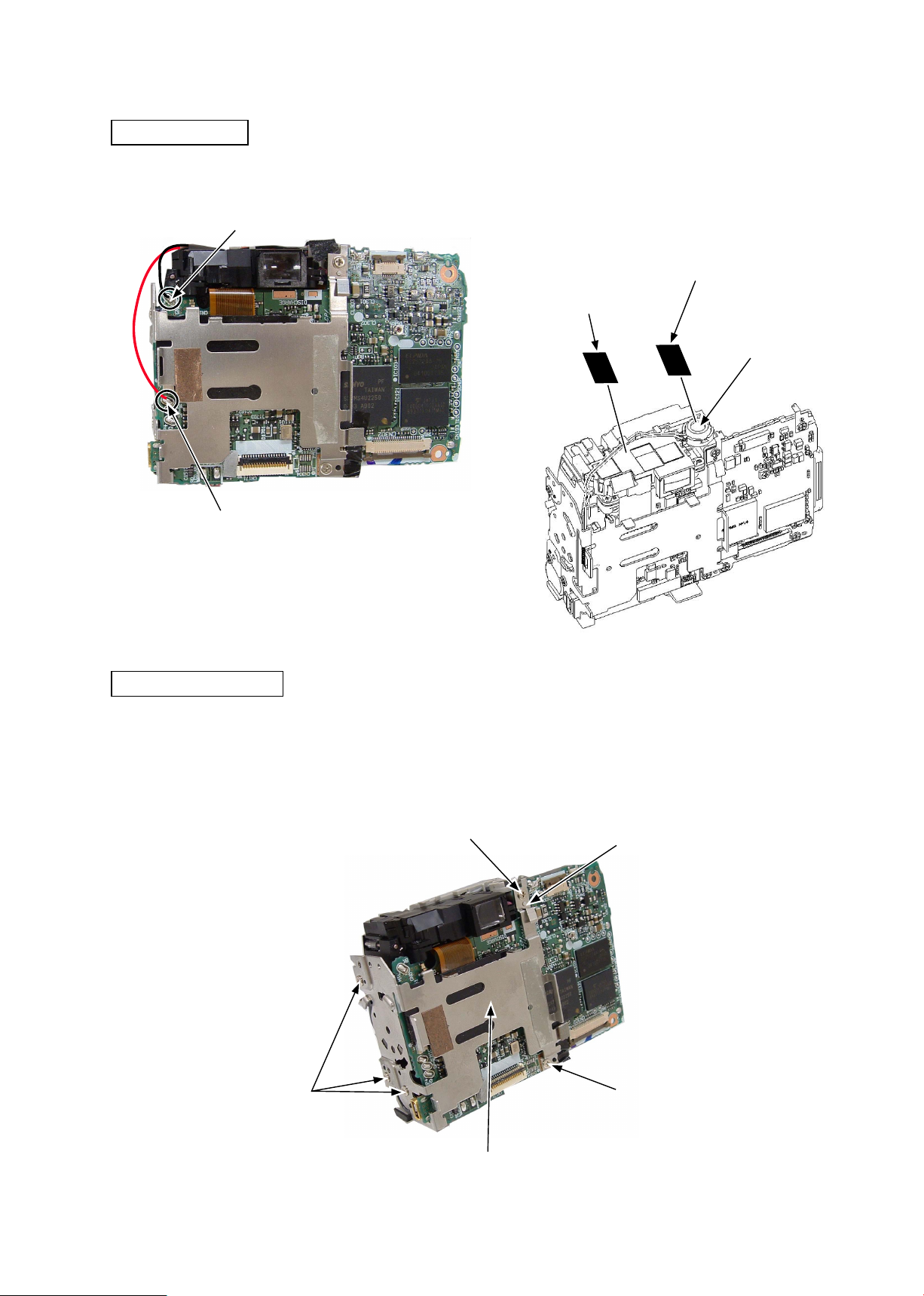
MICROPHONE
・ Unsolder the lead wires [black] and [red]. ・ Take off the spacer [#025].
・ Take off the spacer [#223].
Lead wire [black]
・ Remove the microphone [#222].
Spacer [#223]
Spacer [#025]
VAA31001-R.3651.A
Microphone [#222]
Lead wire [red]
MONITOR HOLDER
・ Remove the two screws [#102].
・ Remove the earth release [#228].
・ Remove the three screws [#104].
・ Remove the LCD holder [#231].
Screw [#102]
Earth release [#228]
Screw [#104]
Screw [#102]
LCD holder [#231]
- D9・ E5600 -
Page 16
VAA31001-R.3651.A
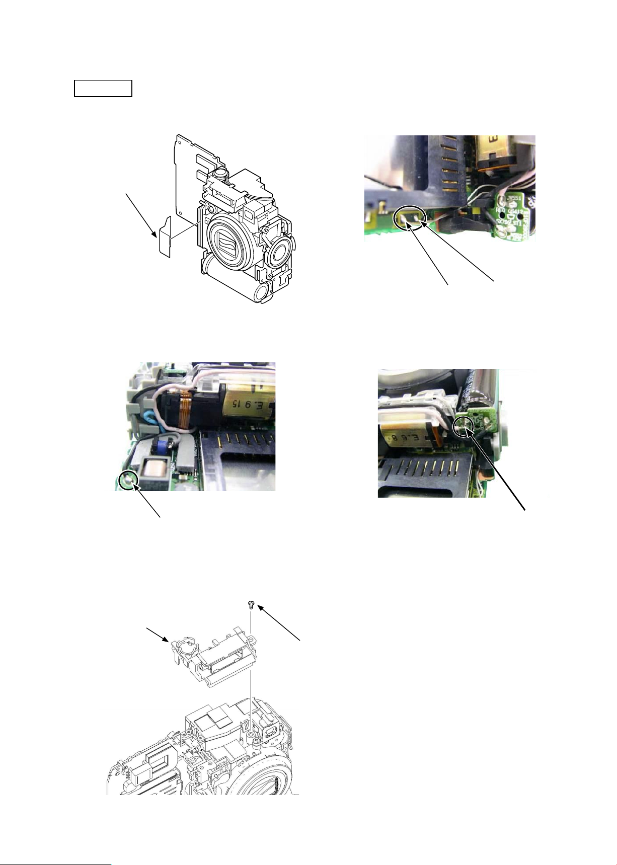
SB UNIT
・ Remove the spacer [#039]. ・ Unsolder the lead wires [gray] and [white].
Spacer [#039]
Lead wires [gray] and [white]
・ Unsolder the lead wire [black]. ・ Unsolder the lead wire [pink].
Lead wire [black]
・ Remove the screw [#104].
・ Float the ash unit [#219].
Flash unit [#219]
Lead wire [pink]
Screw [#104]
- D10 ・ E5600 -
Page 17
VAA31001-R.3651.A
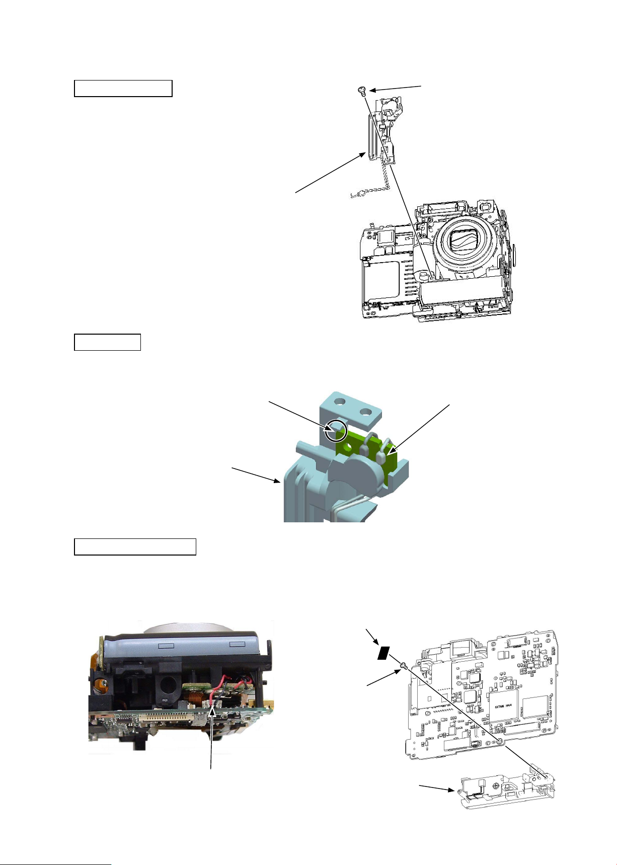
WIRE HOLDER
・ Remove the screw [#102].
・ Remove the wire holder [#215].
Wire holder [#215]
TB-1 PCB
・ Perform unhooking and remove the TB-1 PCB [#216].
Screw [#102]
Hook
Wire holder [#215]
CONDENSER HOLDER
・ Remove the connector. ・ Take off the spacer [#224].
・ Remove the screw [#102].
・ Remove the condenser holder [#204].
Spacer [#224]
TB-1 PCB [#216]
Connector
Screw [#102]
Condenser holder [#204]
- D11 ・ E5600 -
Page 18
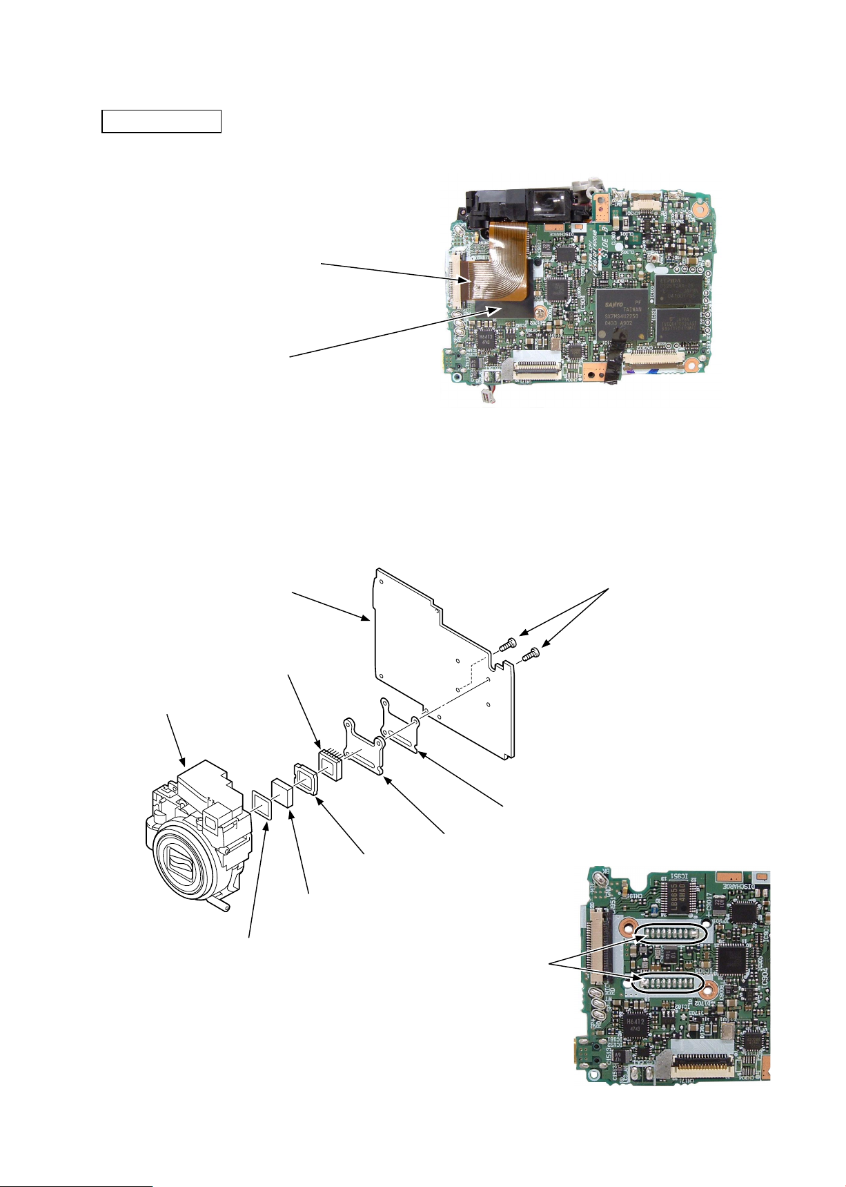
LENS UNIT
・ Remove the FPC.
・ Take off the spacer [#225].
FPC
Spacer [#225]
・ Remove the two screws [#106].
・ The lens unit can be removed.
・ The spacer LPF [#209], the optical lter [#210] and the spacer [#211] can be removed.
・ Remove the solder xing the CCD. (Fig. 1)
・ Remove the CCD [#212], the lens mount [#213] and the spacer insulator [#214].
VAA31001-R.3651.A
Lens unit
Main PCB CP-1 [#218]
CCD [#212]
Optical lter [#210]
Spacer LPF [#209]
Screw [#106]
Spacer insulator [#214]
Lens mount [#213]
Spacer [#211]
Solder
- D12 ・ E5600 -
(Fig. 1)
Page 19

VAA31001-R.3651.A
Points to notice when disassembling / (re)assembling
Lens unit
When the following parts are replaced for repairing the lens unit singularly, the lens unit checking tool is required for the
FFD inspection and adjustment. Therefore, at service facilities where there is no tool, do NOT make a replacement
・1st lens group unit
・2nd lens group unit
・3rd lens group unit
Tools required for FFD inspection and adjustment
Note: When the operation check and adjustment of the lens unit are made for repairing the lens unit singularly,
the following tools are required.
・Lens unit checking tool :J61202
・Connection cable for lens :J61202F
・PCI I/F board :J61204
・Connection cable for PC :J61204A
・Adjusting focus stand for APS :J15327
・Adapter for J15327 :J15327A + J15327D
・E4600/E5600 lens unit checking program :J65072
- D13 ・ E5600 -
Page 20
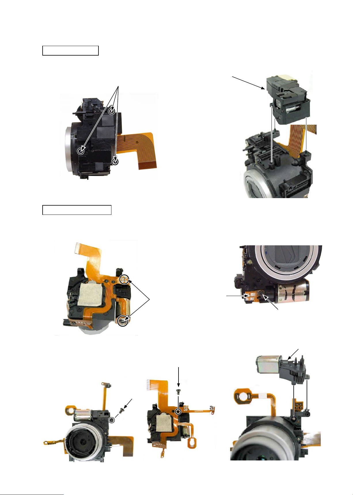
FINDER UNIT
・ Remove the three screws [#429]. ・ Remove the nder unit [#405].
[#405]
Screw [#429]
VAA31001-R.3651.A
ZOOM MOTOR UNIT
・ Remove the solder of the motor at 2 places.
・ Remove the solder of the FPC at 4 places.
Remove the solder.
・ Remove the screw [#429].
・ Remove the screw [#431].
Screw [#431]
・ Remove the screw [#430].
・ Remove the zoom PI.
Zoom PI
・ Remove the zoom motor unit.
Screw [#430]
Zoom motor unit
Screw [#429]
- D14 ・ E5600 -
Page 21
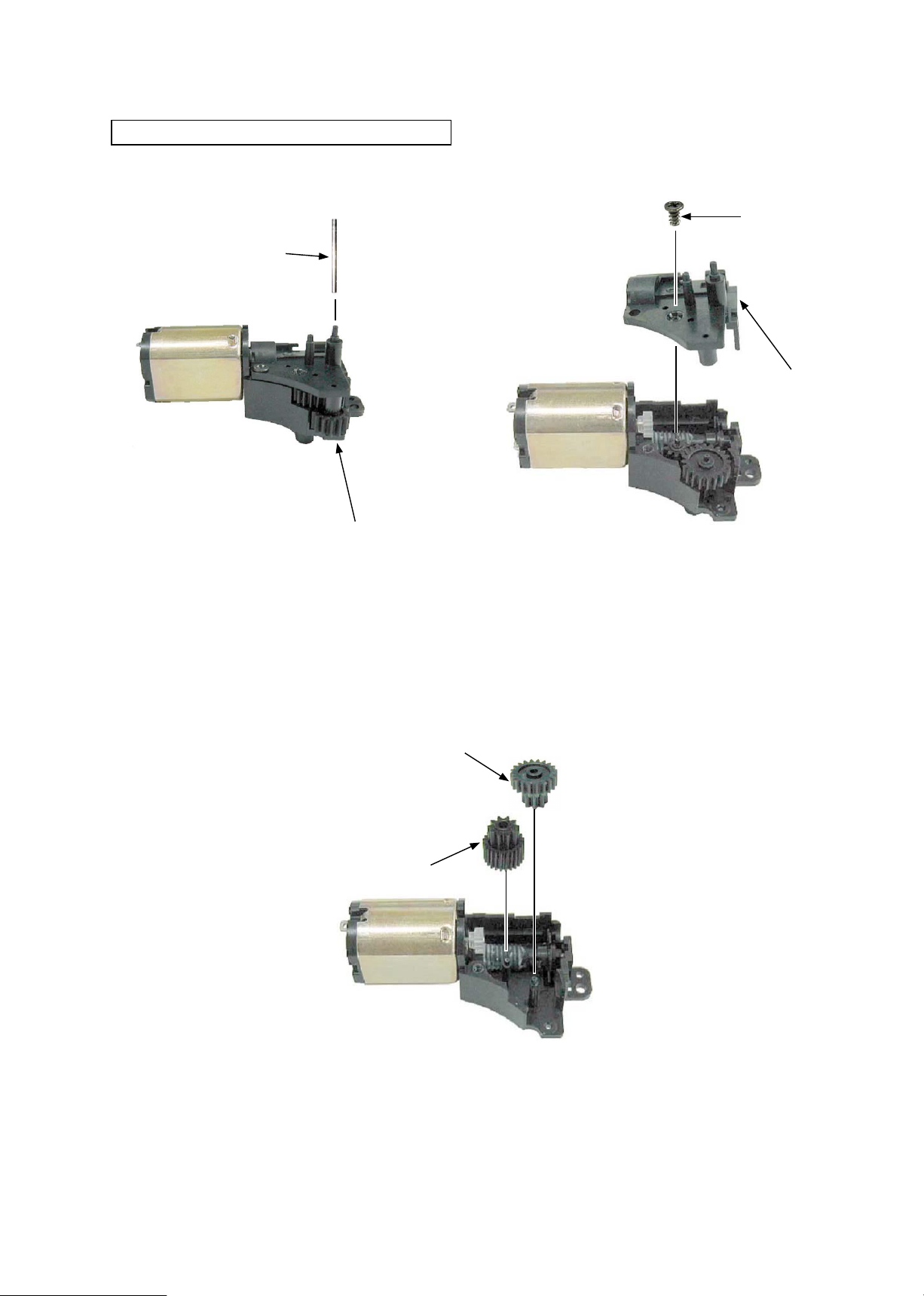
DISASSEMBLY OF ZOOM MOTOR UNIT
VAA31001-R.3651.A
・ Pull out the gear shaft D [#419].
・ Remove the zoom gear E [#411].
Gear shaft D [#419]
Zoom gear E [#411]
・ Remove the screw [#429] and then remove the gear
cover [#403].
Screw [#429]
Gear cover [#403]
・ Remove the zoom gear D [#410] and the zoom gear C [#409].
Zoom gear D [#410]
Zoom gear C [#409]
- D15 ・ E5600 -
Page 22
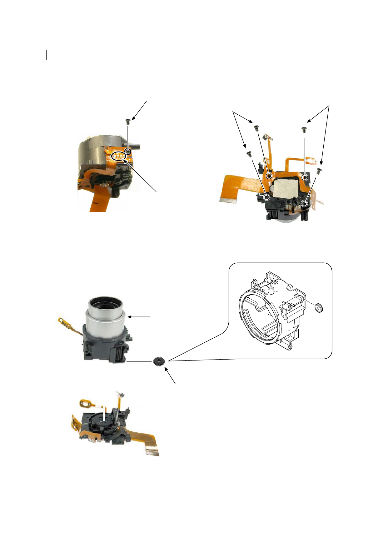
CCD FRAME
VAA31001-R.3651.A
・ Remove the solder.
・ Remove the screw [#430].
Screw [#430]
Solder
・ Remove the four screws [#431].
Screw [#431]
Screw [#431]
・ Remove the lens barrel unit.
・ The nder gear B [#417] can be removed.
Lens barrel unit
Finder gear B [#417]
- D16 ・ E5600 -
Page 23
VAA31001-R.3651.A
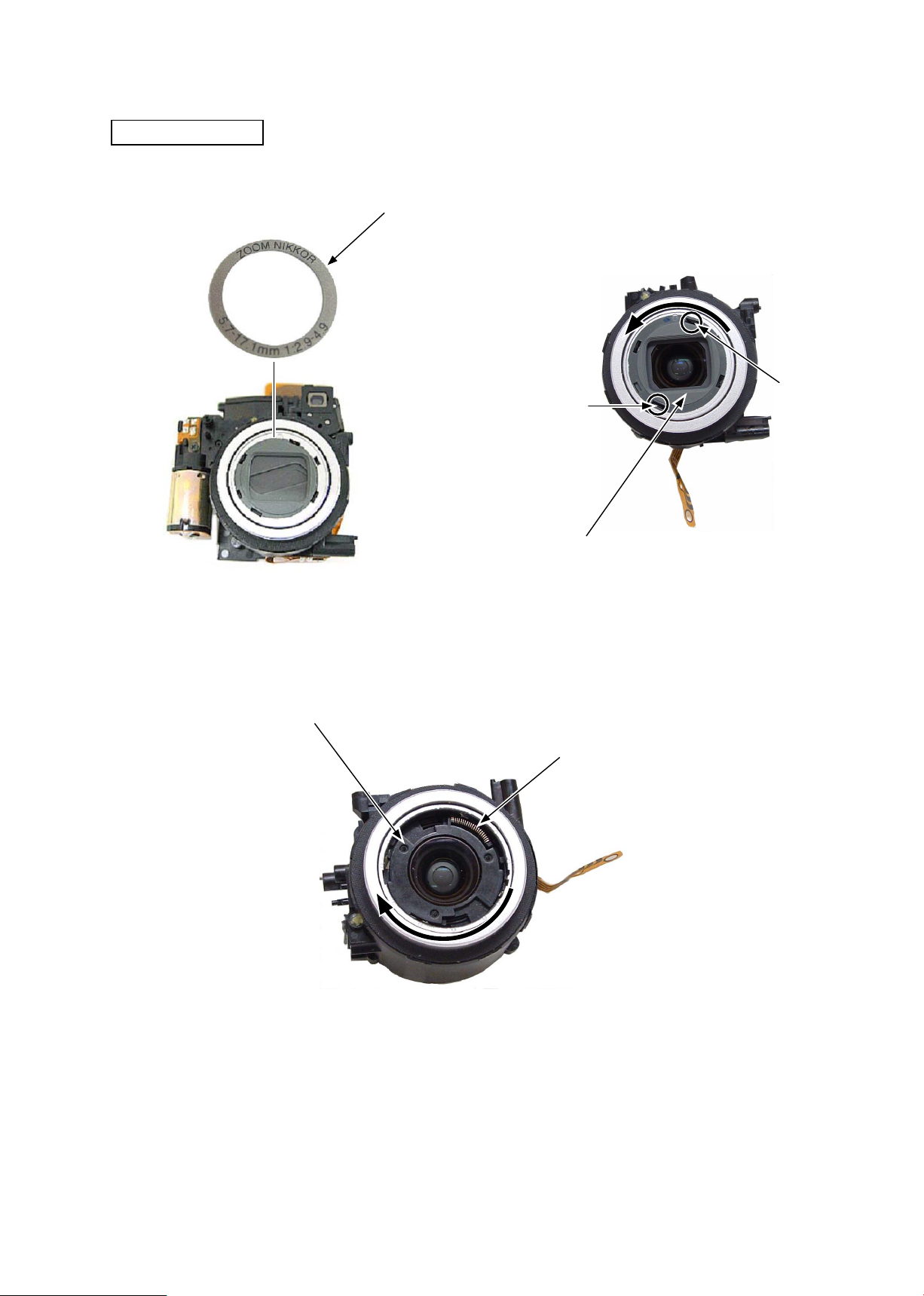
BARRIER UNIT
・ Take off the name plate seal [#415]. ・ Remove the barrier unit [#407] by turning
Name plate seal [#415]
counterclockwise.
※ Insert tweezers into the clearance and turn the
barrier unit counterclockwise. It will be removed
easily.
・ Remove the barrier ring spring [#420].
・ Remove the barrier ring [#404] by turning clockwise.
Barrier ring [#404]
Clearance
Clearance
Barrier unit [#407]
Barrier ring spring [#420]
- D17 ・ E5600 -
Page 24
VAA31001-R.3651.A
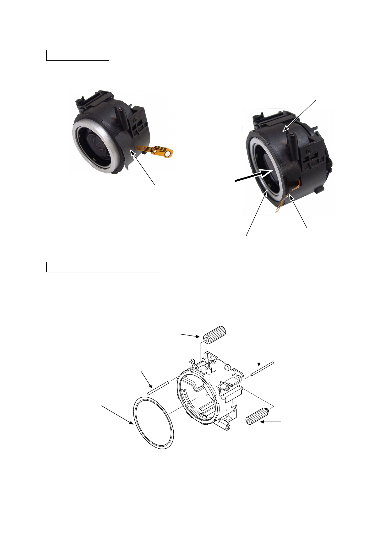
FIXED BARREL
・ Take off the FPC sheet [#423]. ・ Push out the turn barrel [#401]. As taking out the
shutter FPC, remove the turn barrel [#402].
Turn barrel [#402]
FPC sheet [#423]
DISASSEMBLY OF FIXED BARREL
・ Pull out the gear shaft A [#413] and remove the zoom gear F [#412].
・ Pull out the gear shaft B [#418] and remove the nder gear A [#416].
・ Remove the light-shield ring [#424].
Zoom gear F [#412]
Gear shaft A [#413]
Push out.
Turn barrel [#401]
Shutter FPC
Gear shaft B [#418]
Light-shield ring [#424]
Finder gear A [#416]
- D18 ・ E5600 -
Page 25
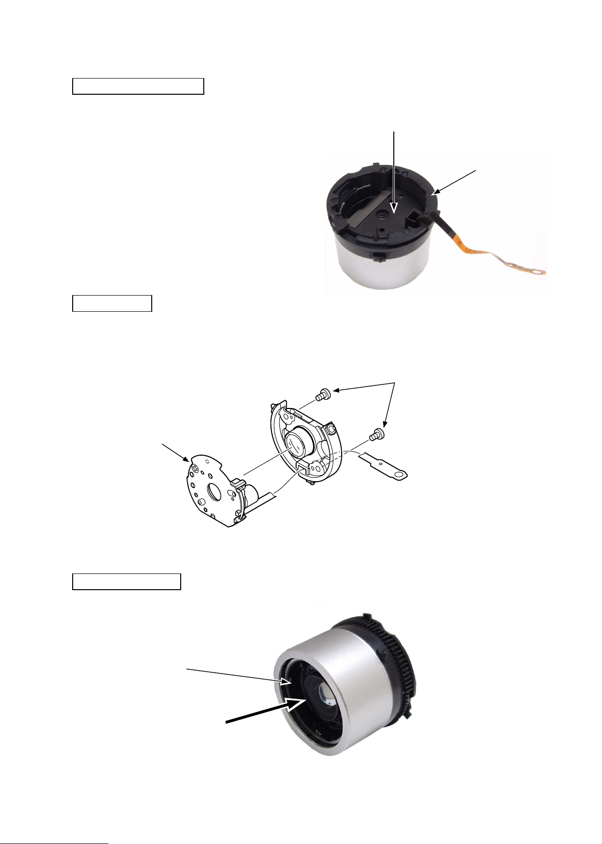
2ND LENS GROUP UNIT
・ Turn the key barrel unit [#428] in the W-end direction to the
limit.
・ The 2nd lens group unit [#426] oats a little and can be
removed.
SHUTTER
・ Remove the two screws [#431].
・ Remove the shutter unit [#432].
VAA31001-R.3651.A
2nd lens group unit [#426]
Key barrel unit [#428]
Shutter unit [#432]
STRAIGHT BARREL
・ Push out and remove the straight barrel unit [#427].
Straight barrel unit [#427]
Screw [#431]
Push out.
- D19 ・ E5600 -
Page 26
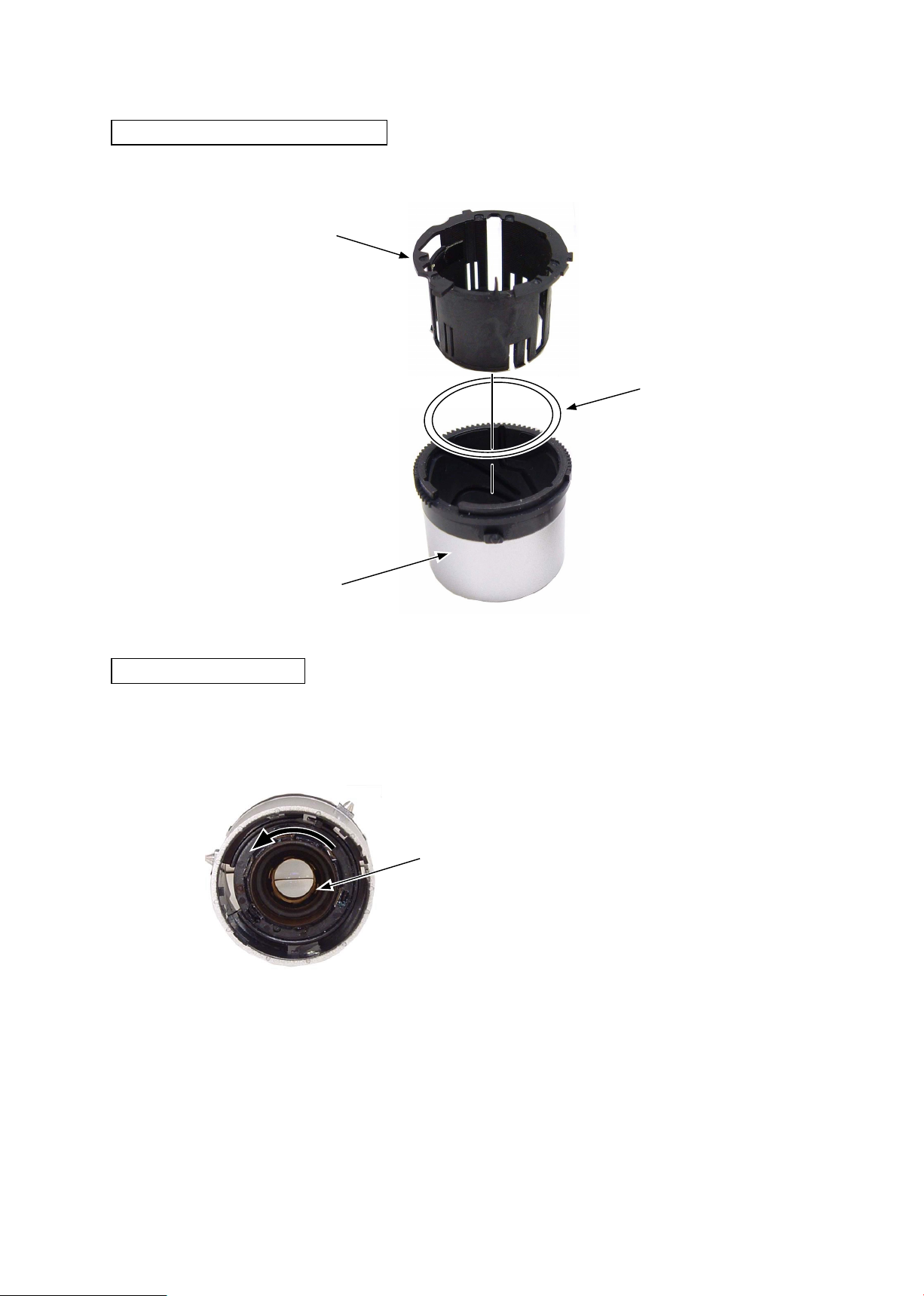
KEY BARREL ・ TURN BARREL
・ Pull out the key barrel unit [#428] from the turn barrel [#401].
Key barrel unit [#428]
VAA31001-R.3651.A
Shading ring [#424]
Turn barrel [#401]
1ST LENS GROUP UNIT
・ Turn the 1st lens group unit [#425] counterclockwise.
・ The 1st lens group unit [#425] can be removed.
1st lens group unit [#425]
- D20 ・ E5600 -
Page 27
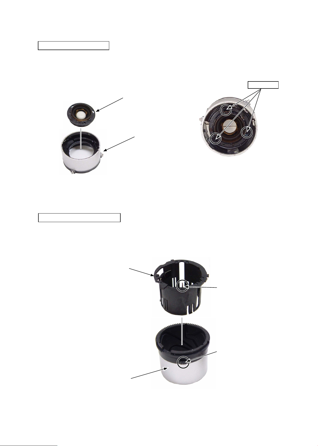
ASSEMBLY
1ST LENS GROUP UNIT
VAA31001-R.3651.A
・ Set the 1st lens group unit [#425] into the straight
barrel unit [#427]. Turn the 1st lens group unit
[#425] counterclockwise to be level and turn it
clockwise to be installed correctly.
1st lens group unit [#425]
Straight barrel unit [#427]
・ Apply the adhesive (1401B) to 3 places.
1401B
KEY BARREL ・ TURN BARREL
・ There is a convex section on the side without gear on the turn barrel [#401]. Fit the lever position on the key barrel
unit [#428] to this convex section and set the key barrel unit [#428] into the turn barrel [#401].
Key barrel unit [#428]
Lever
Convex section
Turn barrel [#401]
- A1・ E5600 -
Page 28
VAA31001-R.3651.A
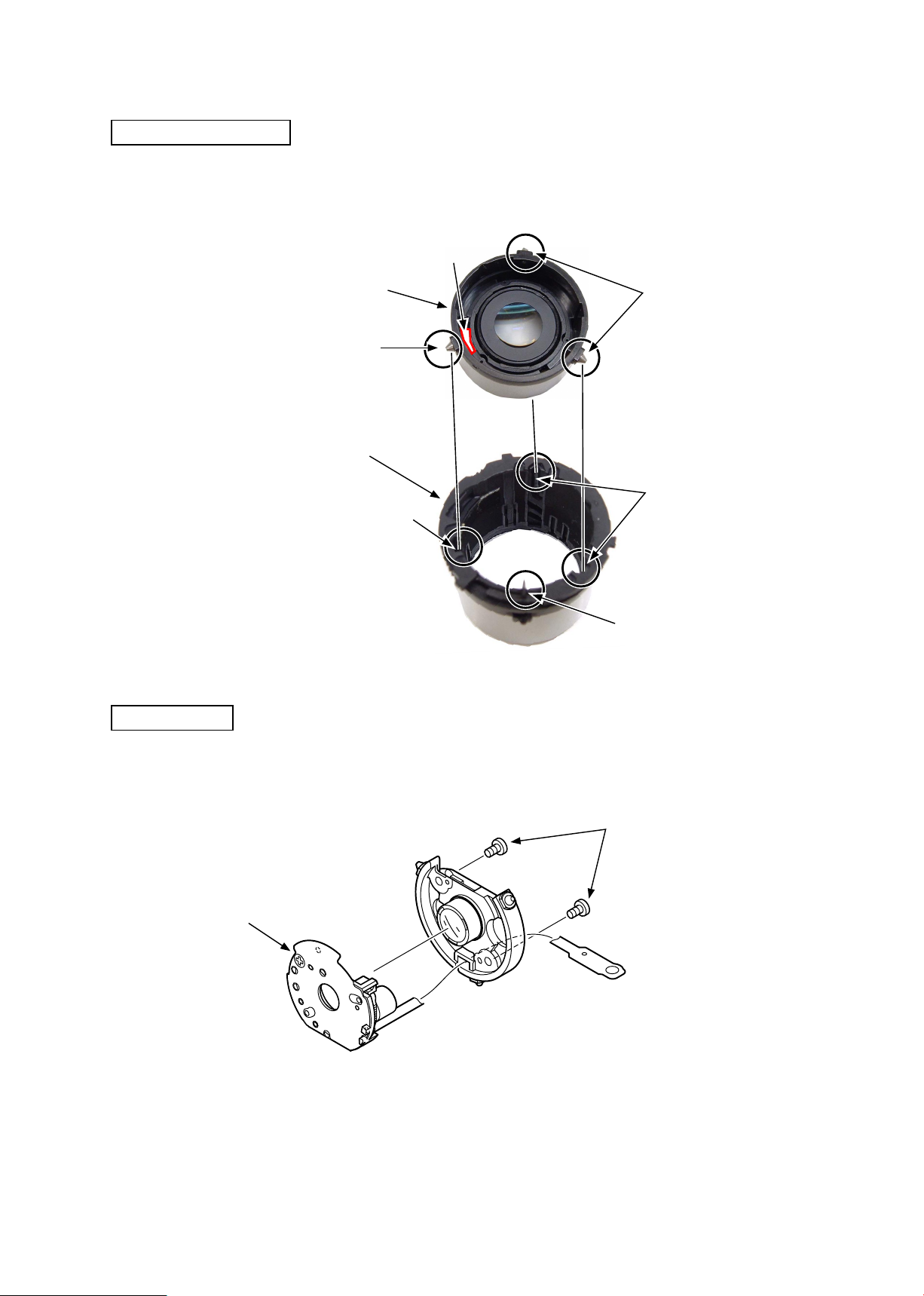
STRAIGHT BARREL
・ Set the lever of the key barrel unit [#428] at the front side. Set the long hole of the straight barrel unit [#427] at the
left side. Fit the convex sections to the grooves and then set the straight barrel unit [#427] into the key barrel unit [#428].
Long hole
SHUTTER
Straight barrel unit [#427]
Convex section
Key barrel unit [#428]
Groove
Convex section
Groove
Lever
・ Install the shutter unit [#432] and tighten the two screws [#431].
Shutter unit [#432]
Screw [#431]
- A2・ E5600 -
Page 29
VAA31001-R.3651.A
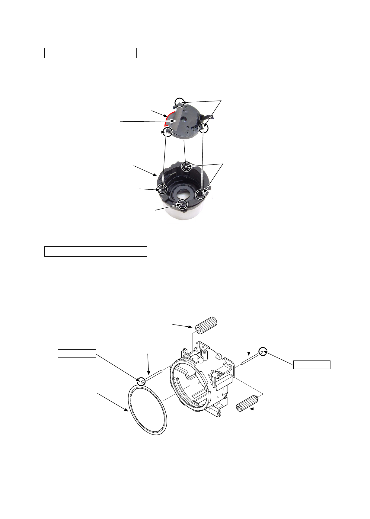
2ND LENS GROUP UNIT
・ Set the lever of the key barrel unit [#428] at the front side. Set the notch of the 2nd lens group unit [#426] at the left
side. Fit the convex sections to the grooves and set the 2nd lens group unit [#426] into the key barrel unit [#428].
Convex section
Notch
2nd lens group unit [#426]
Convex section
key barrel unit [#428].
Groove
Groove
Lever
ASSEMBLY OF FIXED BARREL
・ Set the light-shield ring [#424].
・ Make the stepped difference side of the nder gear A [#416] face the CCD. Then, set the nder gear A [#416] and
insert the gear shaft B [#418].
・ Set the zoom gear F [#412] and insert the gear shaft A [#413].
・ Apply the adhesive (EC-1368) to the gear shafts.
Zoom gear F [#412]
EC-1368
Light-shield ring [#424]
Gear shaft B [#418]
Gear shaft A [#413]
EC-1368
Finder gear A [#416]
- A3・ E5600 -
Page 30
VAA31001-R.3651.A
- A4・ E5600 -
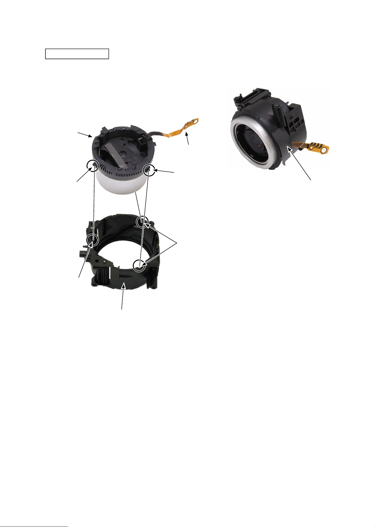
FIXED BARREL
・ Adhere the FPC sheet [#423].・ Insert the shutter FPC into the hole on the side of the
xed barrel [#402].
・ Fit the convex sections on the turn barrel [#401] to
the grooves on the xed barrel [#402]. Set the turn
barrel [#401] into the xed barrel [#402].
FPC sheet [#423]
Turn barrel [#401]
Shutter FPC
Fixed barrel [#402]
Groove
Convex section
Convex section
Groove
Page 31
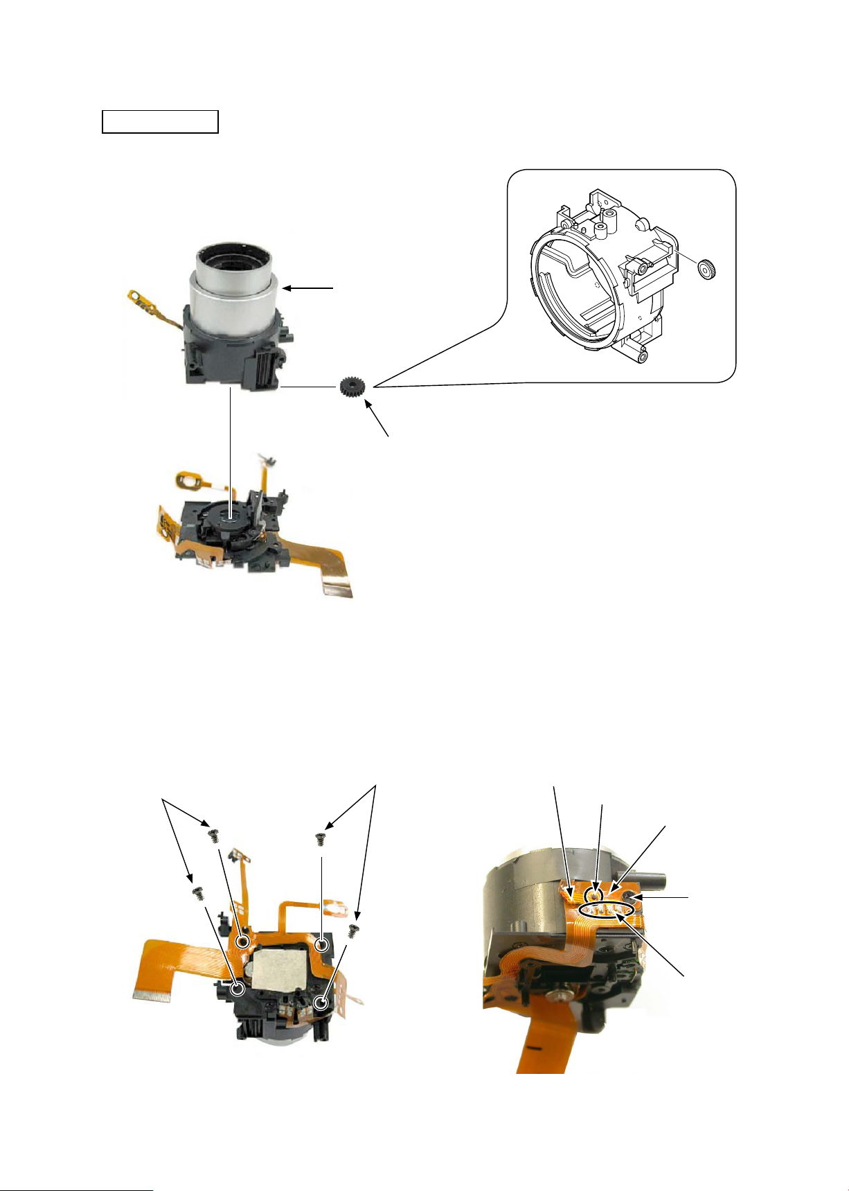
CCD FRAME
・ Set the nder gear B [#417] into the lens barrel unit.
Then, install the lens barrel unit.
Lens barrel unit
Finder gear B [#417]
VAA31001-R.3651.A
・ Tighten the four screws [#431]. ・ Insert the FPC of the CCD frame into the boss.
・ Insert the shutter FPC into the boss.
・ Tighten the screw [#430].
・ Perform soldering.
Screw [#431]
Screw [#431]
Shutter FPC
Boss
FPC of CCD frame
Screw [#430]
Solder
- A5・ E5600 -
Page 32
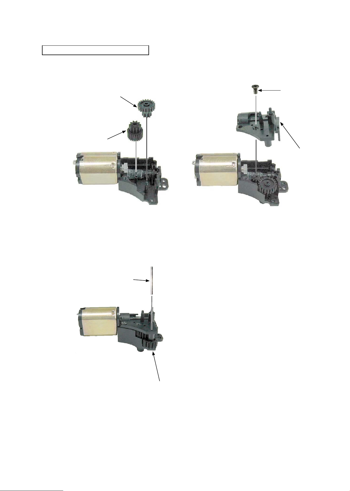
ASSEMBLY OF ZOOM MOTOR UNIT
VAA31001-R.3651.A
・ Set the zoom gear C [#409] and the zoom gear D
[#410].
Zoom gear D [#410]
Zoom gear C [#409]
・ Set the gear cover [#403] and tighten the screw
[#429].
Screw [#429]
Gear cover [#403]
・ Set the zoom gear E [#411] and insert the gear shaft
D [#419].
Gear shaft D [#419]
Zoom gear E [#411]
- A6・ E5600 -
Page 33
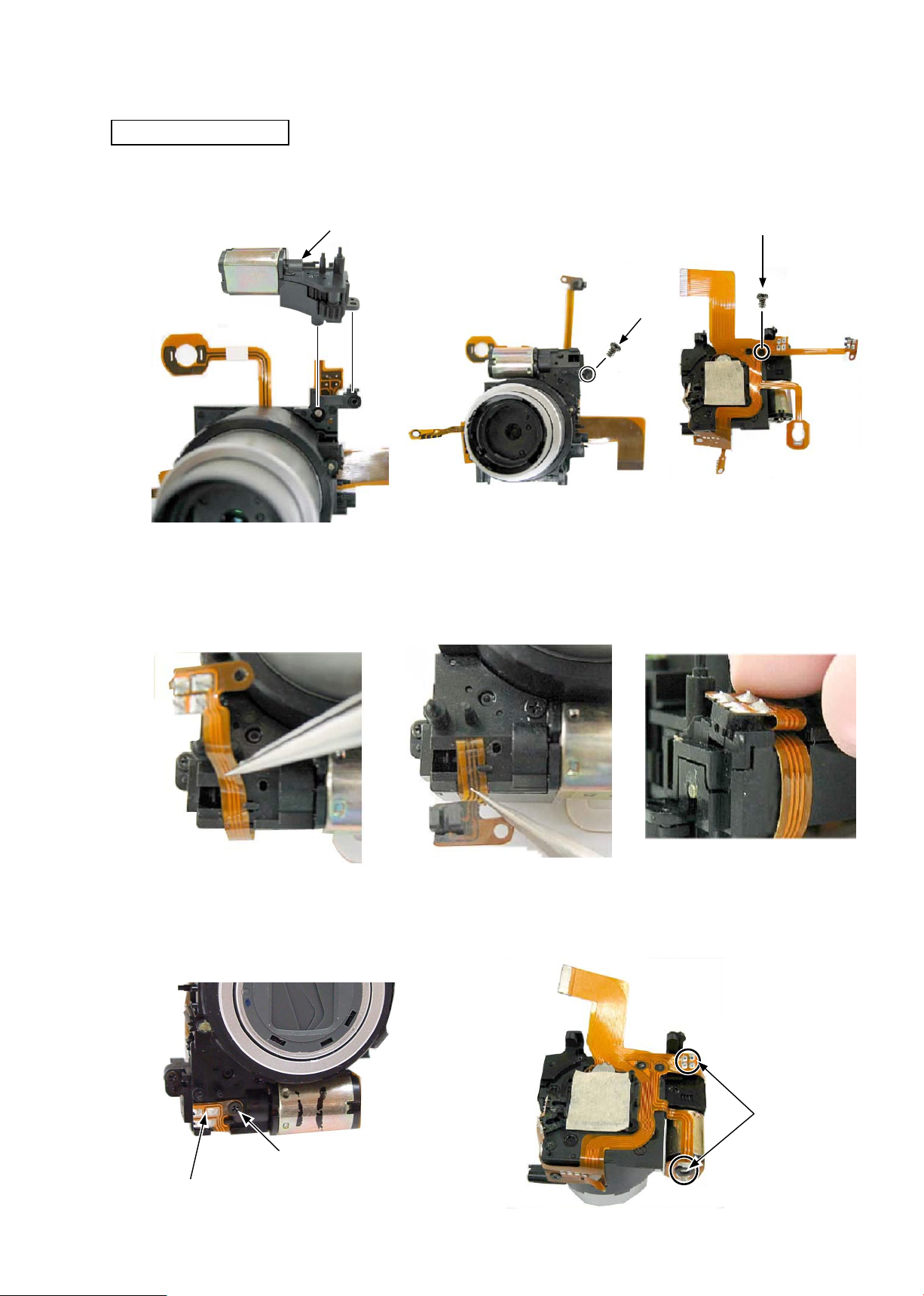
ZOOM MOTOR UNIT
VAA31001-R.3651.A
・ Fit the zoom motor unit to the bosses on the CCD
frame and set it.
Zoom motor unit
・ Tighten the screw [#429].
・ Tighten the screw [#431].
Screw [#431]
Screw [#429]
・ Fold the FPC of the zoom PI as shown below and insert the zoom PI.
(1) (2) (3)
・ Tighten the screw [#430].
・ Solder the FPC at 4 places.
・ Solder the motor at 2 places.
Zoom PI
Perform soldering.
Screw [#430]
- A7・ E5600 -
Page 34
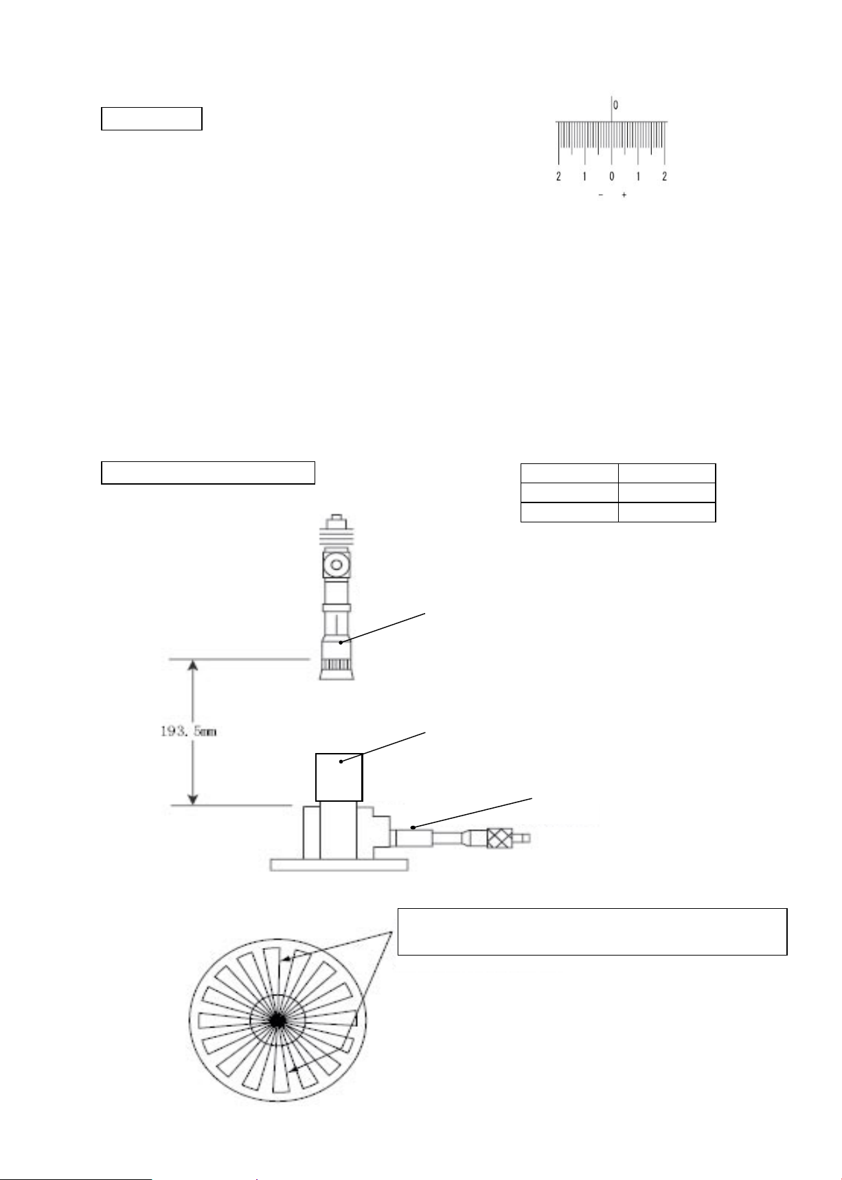
FFD Inspection and adjustment
Preparation
・ Turn the objective glass of the collimator (J19019), and set
degree to 0 (0 mm).
・ Set the 0-position of “Adjusting focus stand for APS (J15327)” as follows:
1. Replace the white acrylic plate of the above stand(J15327)with the new one(J15327A)
2. Install J15327D to the micro stand.
3. Align the upper surface of the white acrylic plate of the Adjusting focus stand (J15327A) with the mirror
reecting surface.
Note: Because the mirror reecting surface is easily damaged, carefully align with it at the same
level by using the dial gauge, etc.
4. Based on the above 0-position, turn the knob of the Adjuting focus stand further to set the -2.16-mm position.
5. Press the reset button of the Adjusting focus stand again, and set the 0-position.
(*FFD:Flange Focal Distance)
VAA31001-R.3651.A
FFD inspection and adjustment
Zoom position FFD standard
Wide-side ± 0.05mm
Tele-side ± 0.05mm
Collimator
Lens-barrel unit
Adjusting focus stand for APS (J15327)
At the position where the color of vertical lines shifts from blue to
red, read the measurement value of the Adjusting focus stand.
- A8・ E5600 -
Page 35
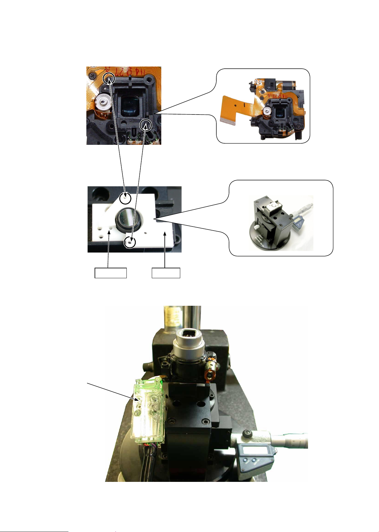
・As shown below, mount the lens-barrel unit on the Adjusting focus stand.
Adjusting focus stand for APS (J15327)
VAA31001-R.3651.A
Lens-barrel unit
J15327A J15327D
・ After mounting the lens-barrel unit on the Adjusting focus stand, connect wires (J61202F) of the lens unit inspection
tool.
Connect wires (J61202F)
- A9・ E5600 -
Page 36
VAA31001-R.3651.A
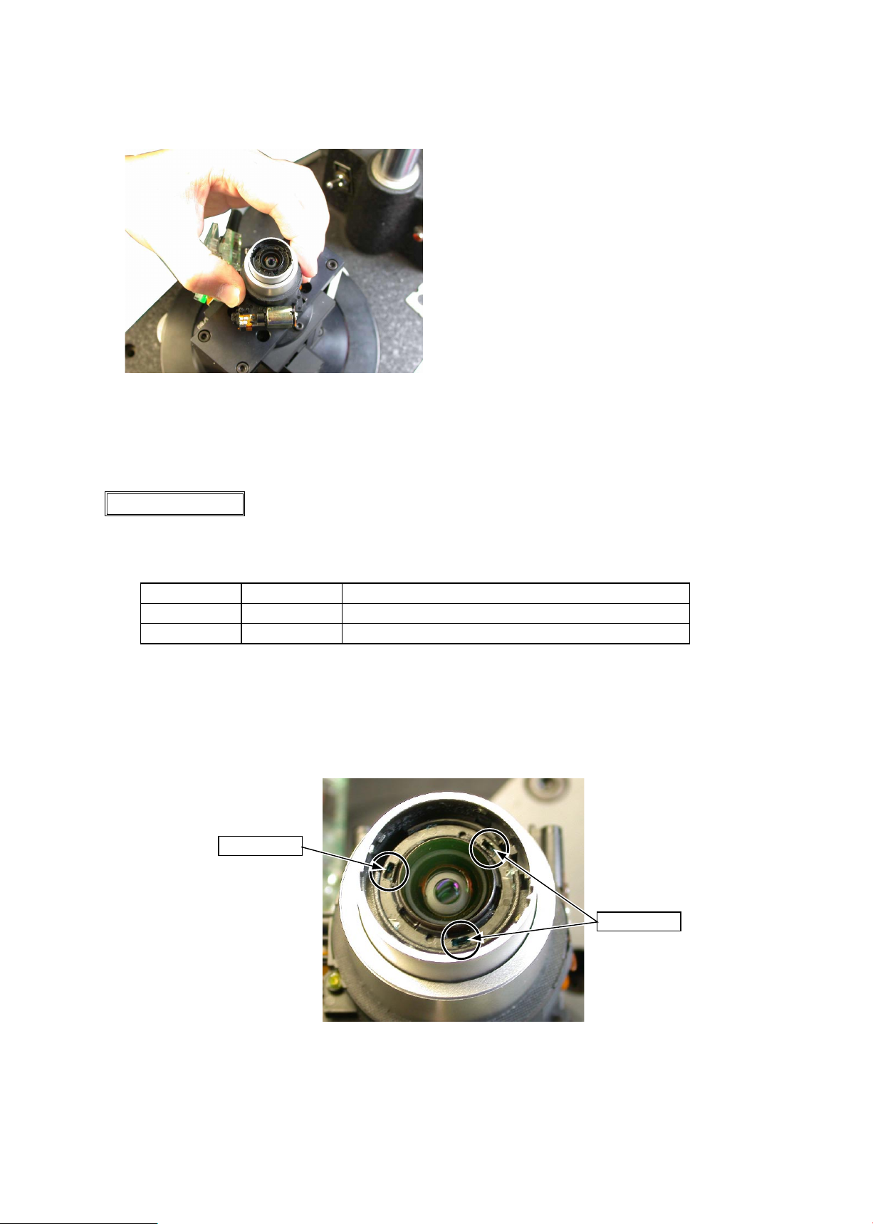
・Hold the lens-barrel unit lightly with a hand, and run the program for inspecting the lens unit.
Note: If the lens-barrel unit is held too tightly,
the FFD value cannot be measured correctly.
Note: Refer to supplied user manuals of the lens unit
checking tool for how to run the program for
inspecting the lens unit.
・ On the main menu of the lens unit checking program, click on "FFD Check" icon, and measure the FFD value
according to instructions of the PC screen.
Note: At the position where the color of vertical lines shifts from blue to red, read the
measurement value of the adjusting focus stand.
FFD adjustment
・ Make adjustment by turning the 1st lens group so that the FFD measured value may be within the standard as shown
below.
Zoom position FFD standard Measured value in relation to reference value (-2.16mm)
Wide-side ± 0.05mm -2.21 ~ -2.11
Tele-side ± 0.05mm -2.21 ~ -2.11
・ Make adjustment at the Tele-side.
・ After the adjustment is nished, apply the screw lock to the 1st lens group unit.
1401B
- A10 ・ E5600 -
1401B
Page 37
BARRIER UNIT
VAA31001-R.3651.A
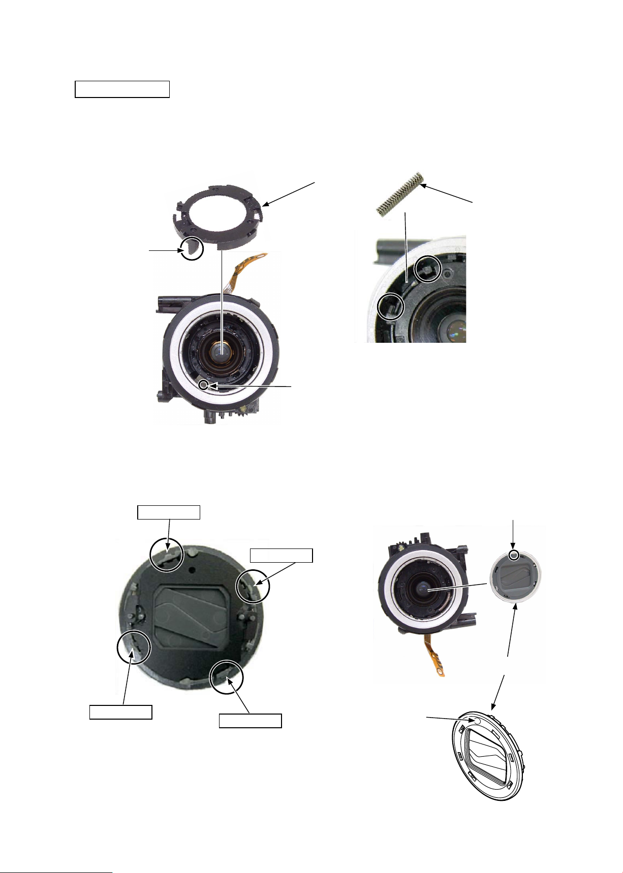
・ Insert the convex section A on the barrier ring [#404]
into the clockwise side of the convex section B in
the lens barrel. Then, set the barrier ring [#404] and
turn it counterclockwise.
Convex section A
・ Set the barrier ring spring [#420].
Barrier ring [#404]
Barrier ring spring [#420]
Convex section B
・ Apply the adhesive (EC-1368) to 4 places on the
back of the barrier unit [#407].
EC-1368
EC-1368
EC-1368
EC-1368
・ Set the barrier unit [#407] with its cav number at the
top side and turn it clockwise.
Cav number
Barrier unit [#407]
Cav number
- A11 ・ E5600 -
Page 38
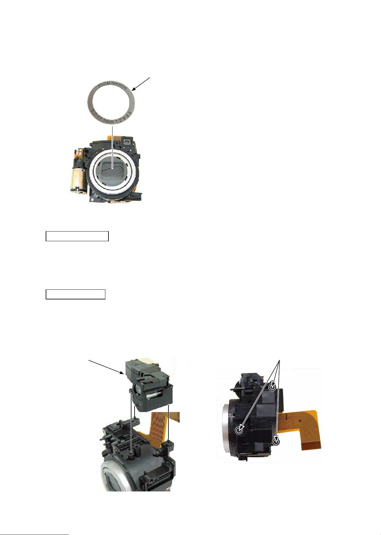
・ Adhere the name plate seal [#415].
Name plate seal [#415]
VAA31001-R.3651.A
Operation inspection
・ It is possible to check the operation with the lens-barrel driving software at the service facilities equipped with the
lens unit checking tool.
FINDER UNIT
・ Set the nder unit [#405] at the W-end manually.
・ Tighten the three screws [#429].
・ Install the nder unit [#405].
[#405] Screw [#429]
- A12 ・ E5600 -
Page 39
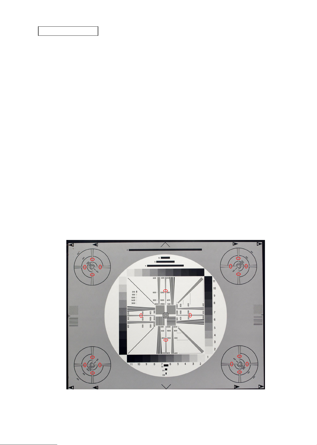
VAA31001-R.3651.A
Resolution inspection
When dissembling and repairing the lens-barrel, be sure to check the following after assembling it into the camera body.
・Resolution inspection
By shooting the high-denition resolution chart (J63079), conrm that the number of TV lines is within the
standard.
TV lines (standard): 1150 TV lines or more in the center; 750 TV lines or more at the periphery
(ref. The resolution is represented by “TV lines”, which are total number of black-and-white strips distin-
guishable on the TV screen.)
(a) To take pictures, set the camera as follows: Shooting-mode (AUTO), Image quality mode (High), Flash
mode (Flash cancel)
(b) Check the zoom position at WIDE, MIDDLE and TELE.
The object distance: WIDE (approx. 0.53 m), MIDDLE (approx. 1.23 m), and TELE (approx.1.6 m).
Set the chart fully screened in the LCD of the camera and x it on a tripod.
(c) Open the shot image by Photoshop, and conrm it by the magnied display, e.g. 100%, etc.
(d) Check if the resolution in the center and the 4 corners of the periphery is identiable in black and white at
the position circled in red as below.
In case the resolution is defective, it is necessary to replace the lens-barrel group unit with the new one.
High-denition resolution chart (J63079)
- A13 ・ E5600 -
Page 40
VAA31001-R.3651.A
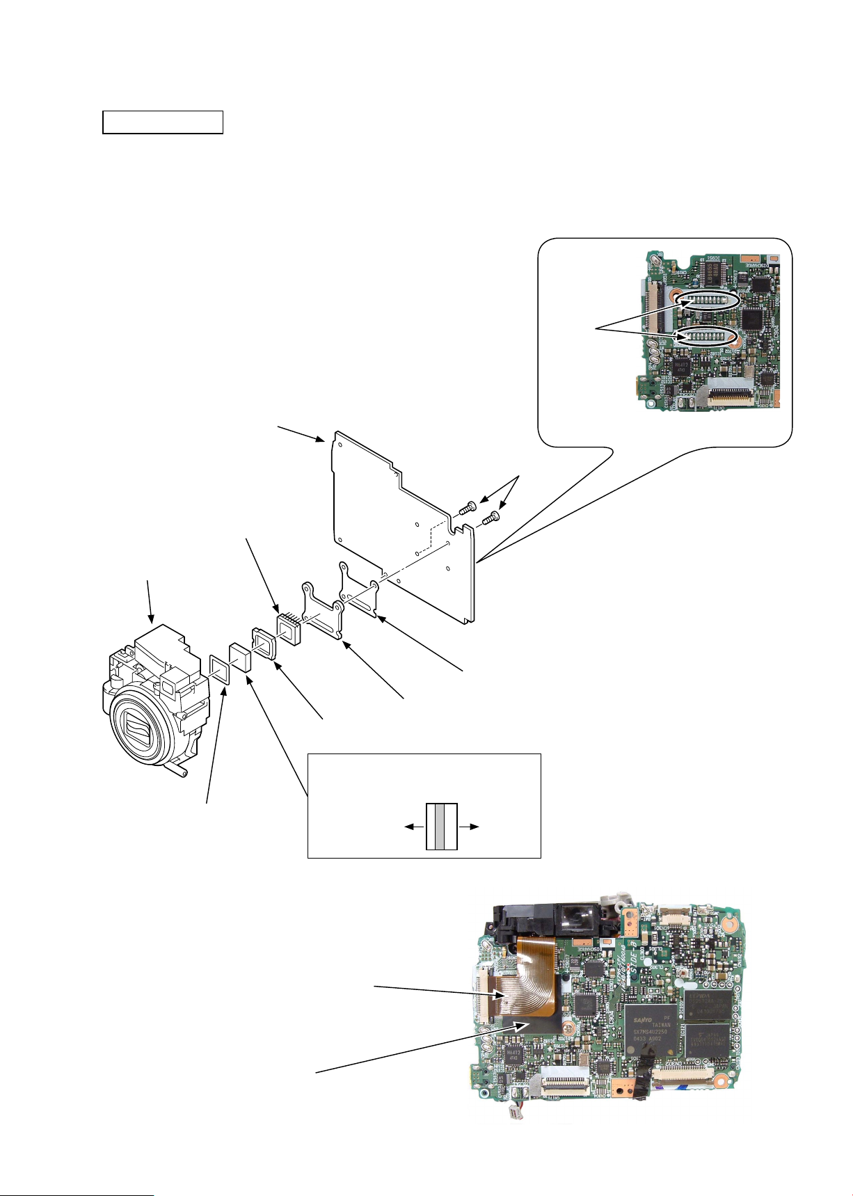
LENS UNIT
・ Set the spacer LPF [#209] and the optical lter [#210] into the lens unit.
・ As taking care about its direction, set the spacer [#211] into the lens unit.
・ Set the spacer insulator [#214], the lens mount [#213] and the CCD [#212] and solder them to the main PCB CP-1
[#218]. (Fig. 1)
・ Tighten the two screws [#106].
Perform
soldering.
Main PCB CP-1 [#218]
(Fig. 1)
Screw [#106]
CCD [#212]
Lens unit
Spacer LPF [#209]
・ Adhere the spacer [#225].
・ Set the FPC.
Spacer [#211]
Lens unit side
Spacer insulator [#214]
Lens mount [#213]
Optical lter [#210]
Setting direction
CCD
side
Spacer [#225]
FPC
- A14 ・ E5600 -
Page 41
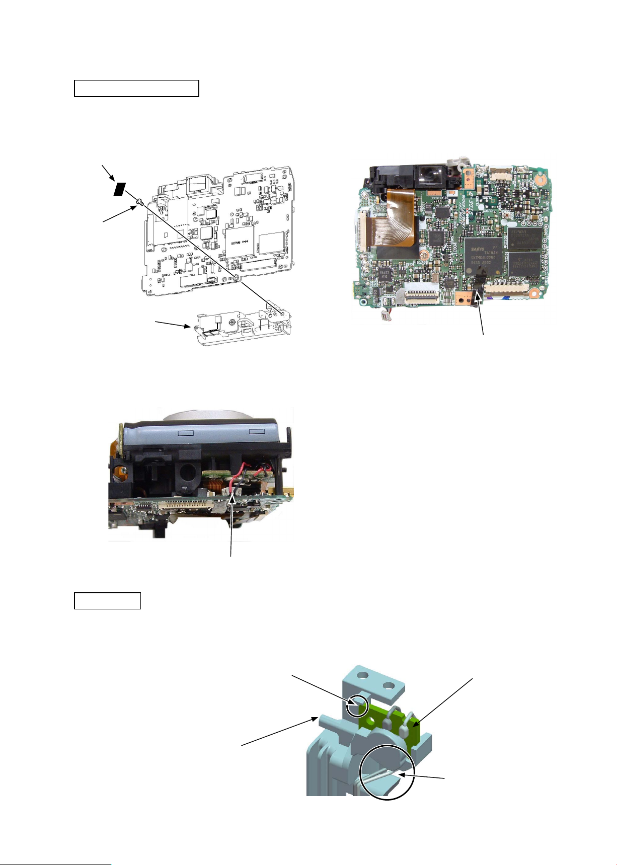
CONDENSER HOLDER
VAA31001-R.3651.A
・ Set the condenser holder [#204] and tighten the
screw [#102].
Spacer [#224]
Screw [#102]
Condenser holder [#204]
・ Set the connector without crossing the cords above
the connector and the PCB.
・ Adhere the spacer [#224].
Spacer [#224]
Connector
TB-1 PCB
・ Set the TB-1 PCB [#216] onto the hook of the wire holder [#215].
・ Pass the lead wire of the TB-1 PCB [#216] through the notch of the wire holder [#215].
Hook
Wire holder [#215]
- A15 ・ E5600 -
TB-1 PCB [#216]
Notch
Page 42
VAA31001-R.3651.A
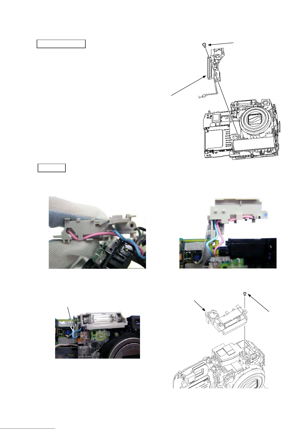
WIRE HOLDER
・ Set the wire holder [#215] and tighten the screw
[#102].
Wire holder [#215]
SB UNIT
・ Arrange the lead wires [pink] and [blue] as shown below.
Screw [#102]
・ As arranging the lead wire [blue] as shown below (Fig. 1), set the ash unit [#219] and tighten the screw [#104]. (Fig. 2)
Flash unit [#219]
Lead wire [blue]
Screw [#104]
(Fig.1)
(Fig.2)
- A16 ・ E5600 -
Page 43
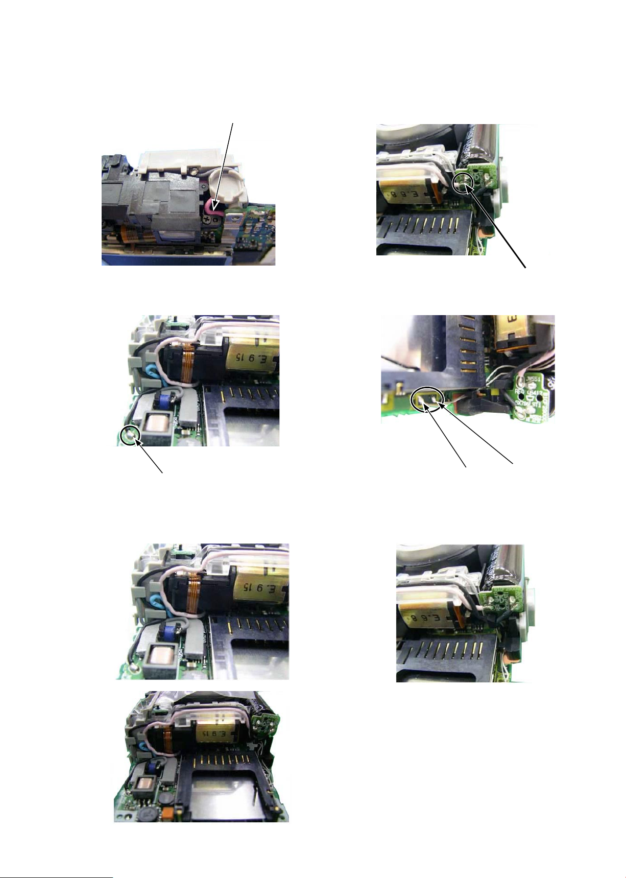
・ Arrange the lead wire [pink] as shown below. ・ Solder the lead wire [pink].
Lead wire [pink]
・ Solder the lead wires [gray] and [white].・ Solder the lead wire [black].
VAA31001-R.3651.A
Lead wire [pink]
Lead wire [black]
・ Arrange the lead wires as shown below.
Lead wires [gray] and [white]
- A17 ・ E5600 -
Page 44
・ Adhere the spacer [#039].
Spacer [#039]
MONITOR HOLDER
VAA31001-R.3651.A
・ Fit the LCD holder [#231] to the bosses, set it and tighten the three screws [#104].
・ Set the earth release [#228].
・ Tighten the two screws [#102].
Screw [#102]
Boss
crew [#104]
Boss
Screw [#104]
LCD holder [#231]
Earth release [#228]
Screw [#102]
- A18 ・ E5600 -
Page 45
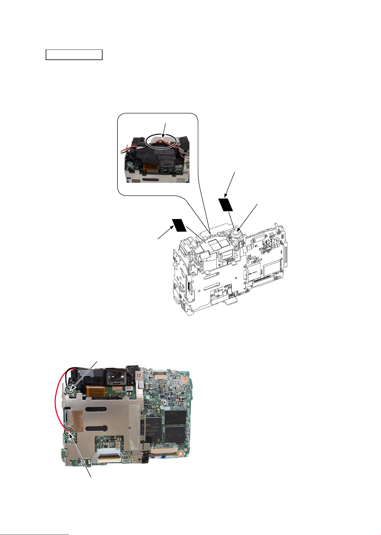
MICROPHONE
・ Set the microphone [#222].
・ Set the lead wires [black] and [red] onto the hook without crossing them. (Fig. 1)
・ Set the spacer [#223].
・ Set the spacer [#025].
Set the lead wires onto the
hook.
Spacer [#223]
(Fig.1)
Microphone [#222]
VAA31001-R.3651.A
Spacer [#025]
・ Solder the lead wires [black] and [red].
Lead wire [black]
Lead wire [red]
- A19 ・ E5600 -
Page 46
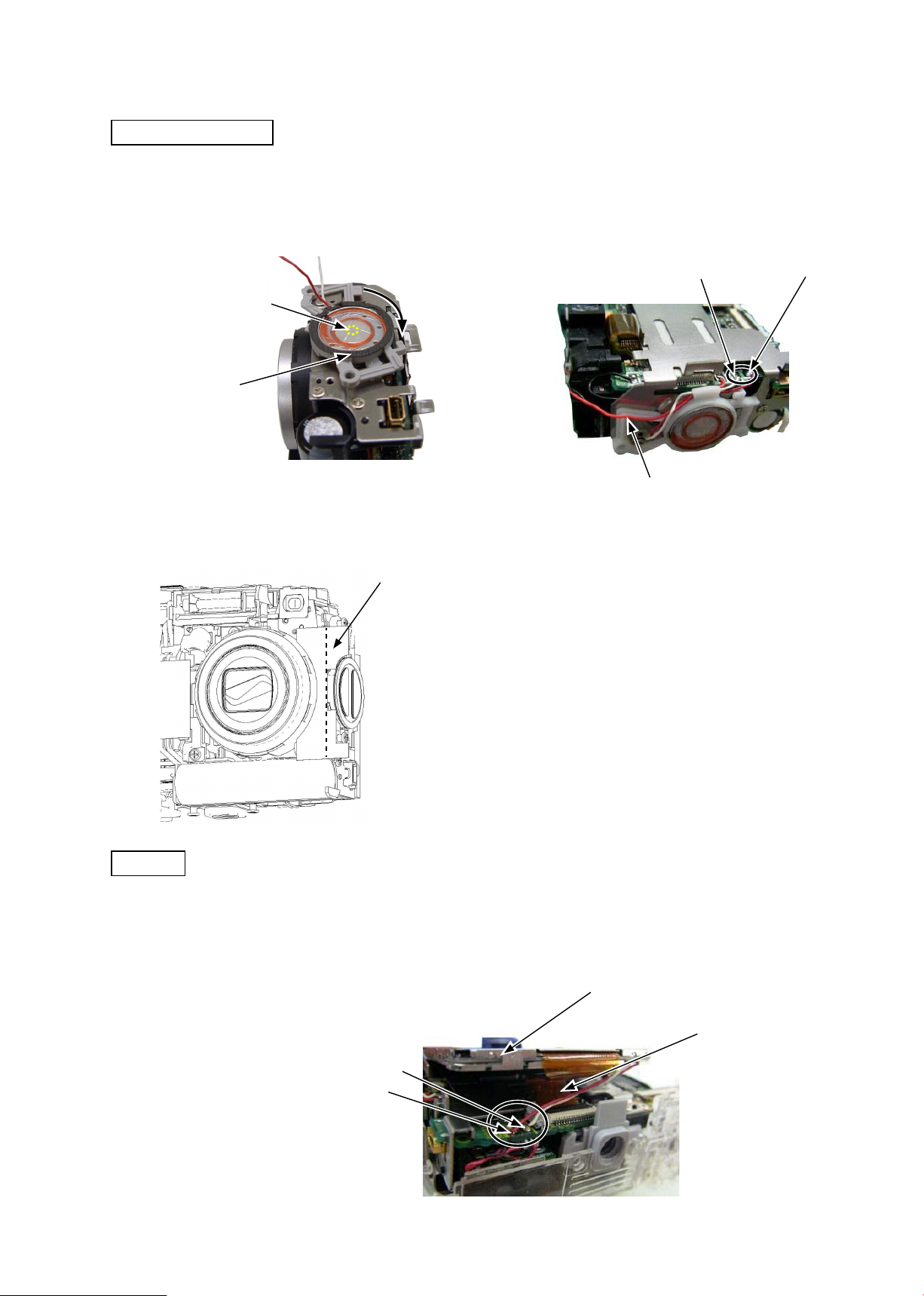
SPEAKER HOLDER
VAA31001-R.3651.A
・ Fit the center boss on the speaker holder [#233] into
the boss hole on the LCD holder [#231]. Then, turn
the speaker holder [#233] clockwise.
Boss hole position
Speaker holder
[#233]
・ Adhere the spacer [#206].
Spacer [#206]
・ Solder the lead wires [red] and [white].
・ Arrange the lead wire [red] of the microphone [#222]
and the lead wires [red] and [white] of the speaker
as shown below.
Lead wire [white]
Lead wire [red] of microphone [#222]
Lead wire [red]
LCD
・ Set the FPC.
・ Solder the lead wires [red] and [white].
・ Arrange the lead wires [red] and [white] as shown below. Fold the FPC and set the LCD [#239].
LCD [#239]
FPC
Lead wires [white]
Lead wires [red]
- A20 ・ E5600 -
Page 47
VAA31001-R.3651.A
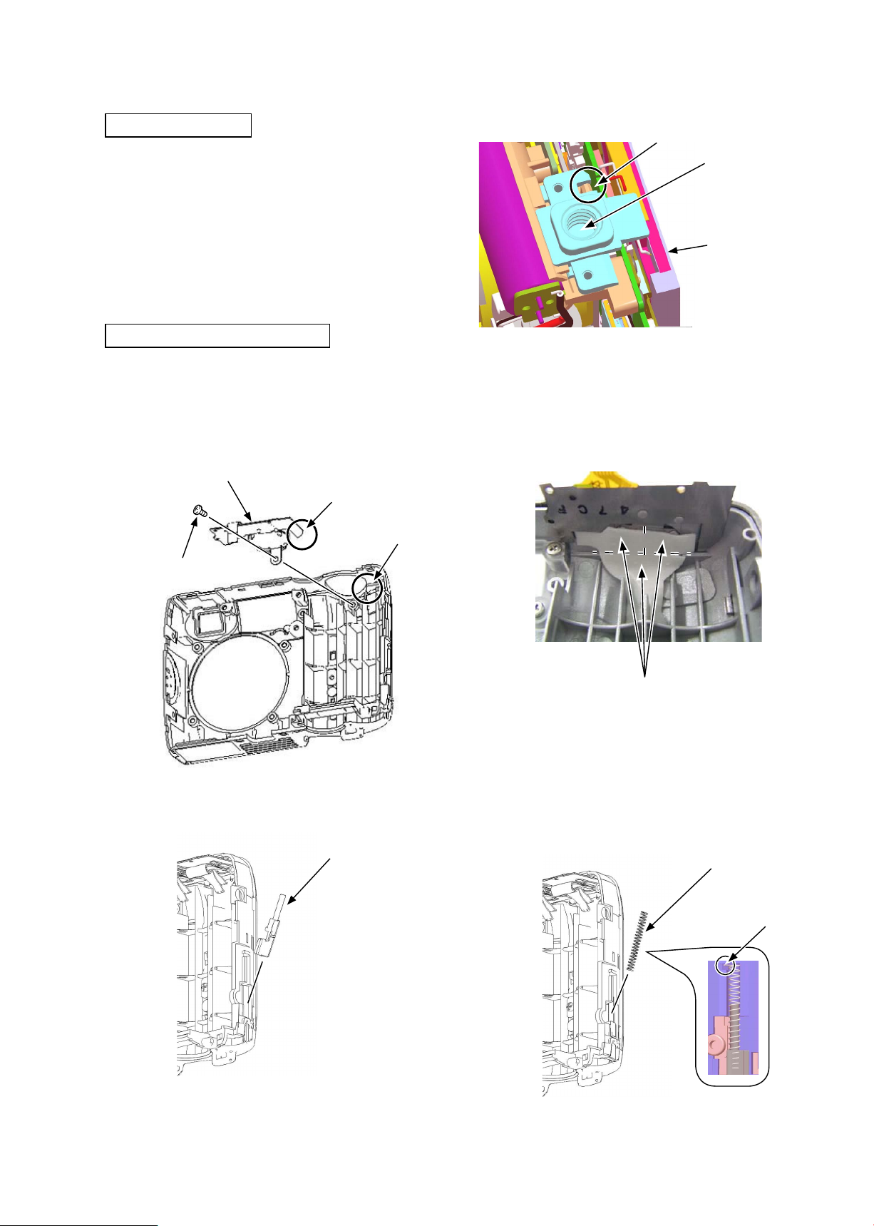
TRIPOD SOCKET
・ Install the tripod socket [#201] by tting onto the
hook.
ASSEMBLY OF FRONT COVER
・ Install the release button unit [#020] by inserting its
convex section A into the notch B on the front cover
[#013].
・ Tighten the screw [#104].
Release button unit [#020]
Convex section A
Notch B
Hook
Tripod socket [#201]
LCD [#239]
・ Adhere the spacer [#019] of the release button unit
as shown below.
※ The spacer [#019] is divided into three pieces from
the dotted line in the gure.
Screw [#104]
・ Set the DC cover [#011].
DC cover [#011]
Spacer [#019]
・ Set the DC cover spring [#012].
DC cover spring [#012]
Set the convex section at
the top side.
- A21 ・ E5600 -
Page 48
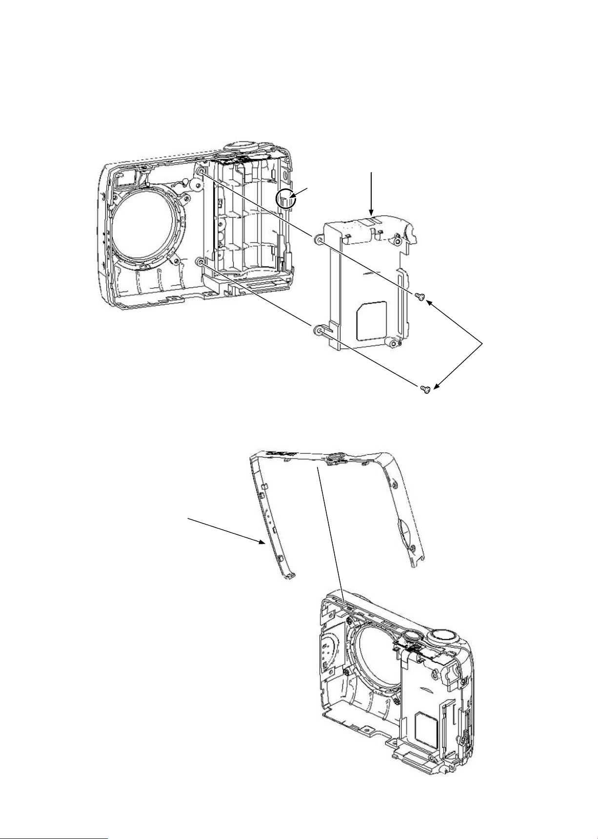
・ Set the battery holder [#024] by using the hook.
・ Tighten the two screws [#104].
VAA31001-R.3651.A
Battery holder [#024]
Hook
・ Set the decoration top [#021].
Decoration top [#021]
Screw [#104]
- A22 ・ E5600 -
Page 49
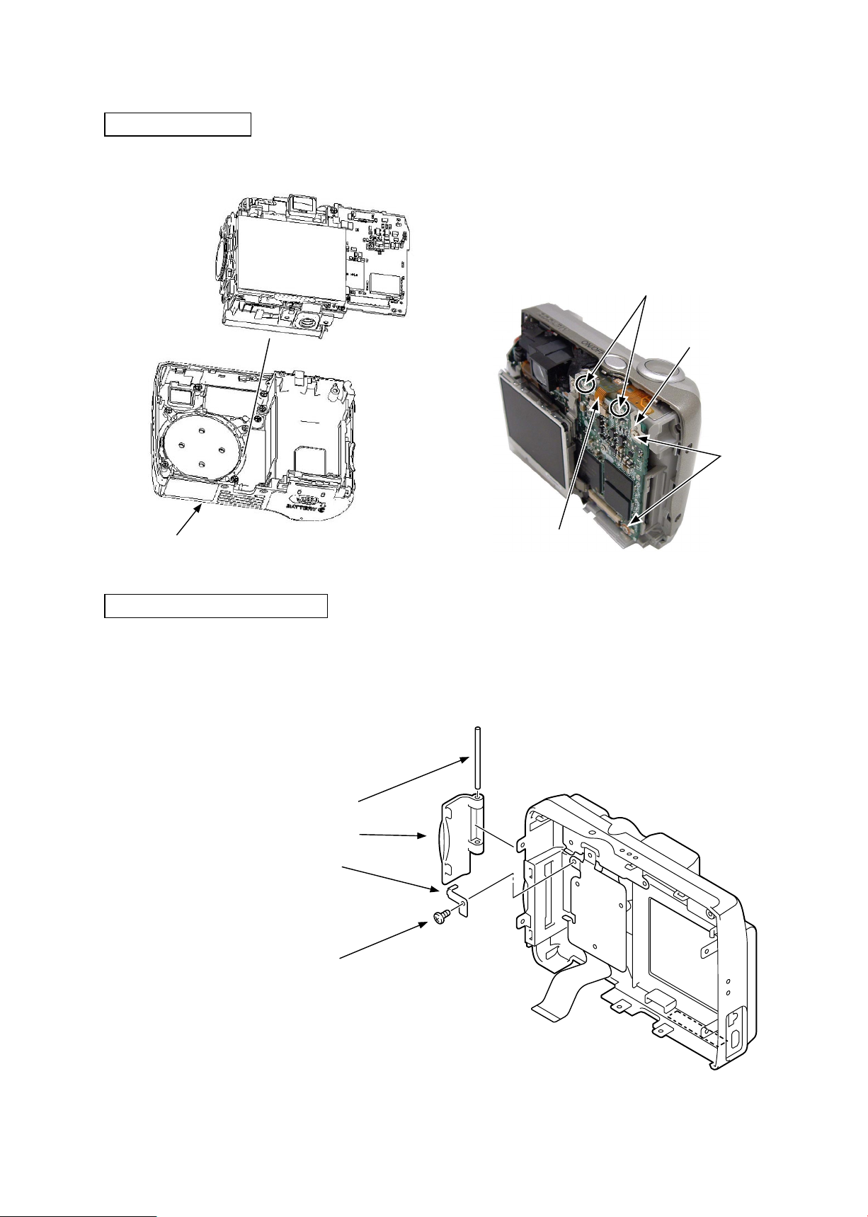
FRONT COVER
VAA31001-R.3651.A
・ Set the front cover [#013].
Front cover [#013]
・ Set the earth release [#026].
・ Tighten the two screws [#102].
・ Perform soldering.
・ Set the FPC.
Perform soldering.
Earth release [#026]
Screw [#102]
FPC
ASSEMBLY OF REAR COVER
・ Set the SD cover [#037].
・ Set the cover shaft [#009].
・ Set the earth shaft [#029].
・ Tighten the screw [#104].
Cover shaft [#009]
SD cover [#037]
Earth shaft [#029]
Screw [#104]
- A23 ・ E5600 -
Page 50
VAA31001-R.3651.A
- A24 ・ E5600 -
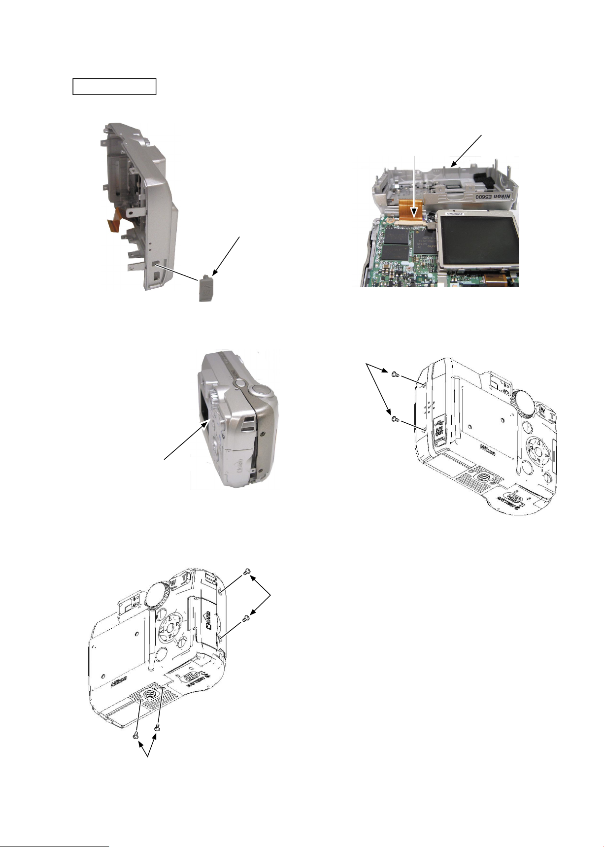
・ Fold the FPC as shown below and set it.
FPC
Rear cover unit [#030]
・ Set the USB cover [#033].
REAR COVER
・ Tighten the two screws [#103].・ Set the rear cover unit [#030].
Rear cover unit [#030]
・ Tighten the four screws [#102].
USB cover [#033]
Screw [#102]
Screw [#102]
Screw [#103]
Page 51

ADJUSTMENT
1. Equipment
IBM compatible PC/AT • AC adapter EH-62B • USB cable ( UC-E6)
2. Servicing tools
• Pattern box • Color meter • Luminance meter • Siemens star chart • Calibration software (J65071)
• Adjustment collimator (J63090) or Adjustment rmware
3. Adjustment items and order
Adjustment after replacing the CP-1 PCB of RP
1. Writing of the initial image data
2. Firmware up
3. Lens adjustment
4. AWB adjustment
5. CCD white dot defect compensation
6. CCD black dot/white dot defect adjustment
VAA31001-R.3651.A
7. USB storage information registration
Note) If replacing the lens, CCD, optical lter, it is necessary to perform the above 3-7 adjustments again. 4 -6
adjustments should be made in the above order.
- A25 ・ E5600 -
Page 52
VAA31001-R.3651.A
4. Initial image data writing and Firmware upgrading
Write the data of initial images, and go on to upgrade the rmware.
Device
・ AC adapter (EH-62B)
・ Upgrading SD card X 1
[How to create an upgrading SD card]
1) Format SD card on PC.
2) Create a folder named "rmware" in the root directory of the SD card.
3) Copy "rmware.bin" into the created folder.
4) Copy "nanddat.bin" into the root directory of the same SD card.
Note) When only rmware upgrading is performed without replacing CP-1 PCB, copying "nanddat.bin" into the SD card is
NOT necessary.
Procedure
・ Turn the camera OFF and connect the AC adapter.
・ Insert the upgrading SD card into camera.
・ Set the mode dial to "SETUP" and turn power ON.
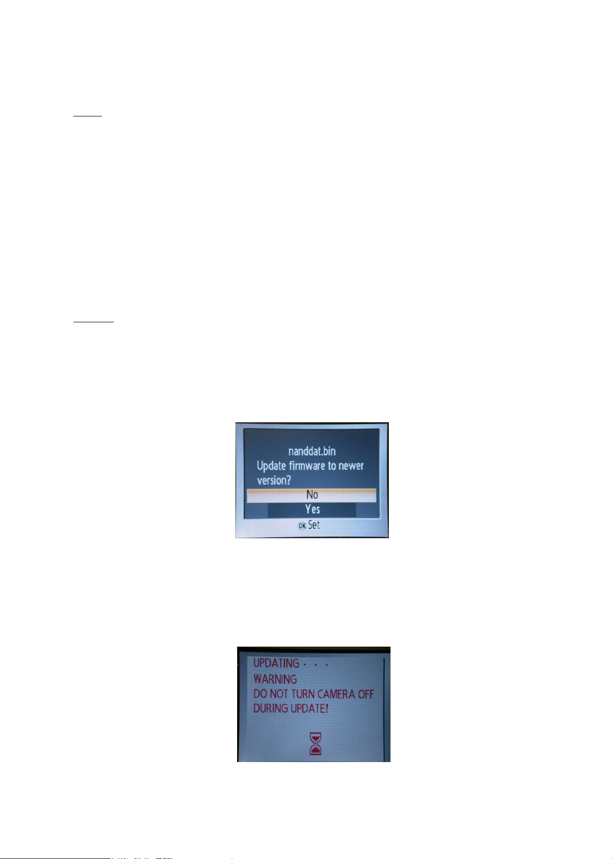
・ Highlight and select "Firmware version" to display the menu for data-writing of initial images. (Fig.1)
・ Select "Yes", and press the decision button to carry out data-writing of initial images. (Fig.2)
Note: Do NOT turn power OFF during upgrading.
(Fig.1)
(Fig.2)
- A26 ・ E5600 -
Page 53
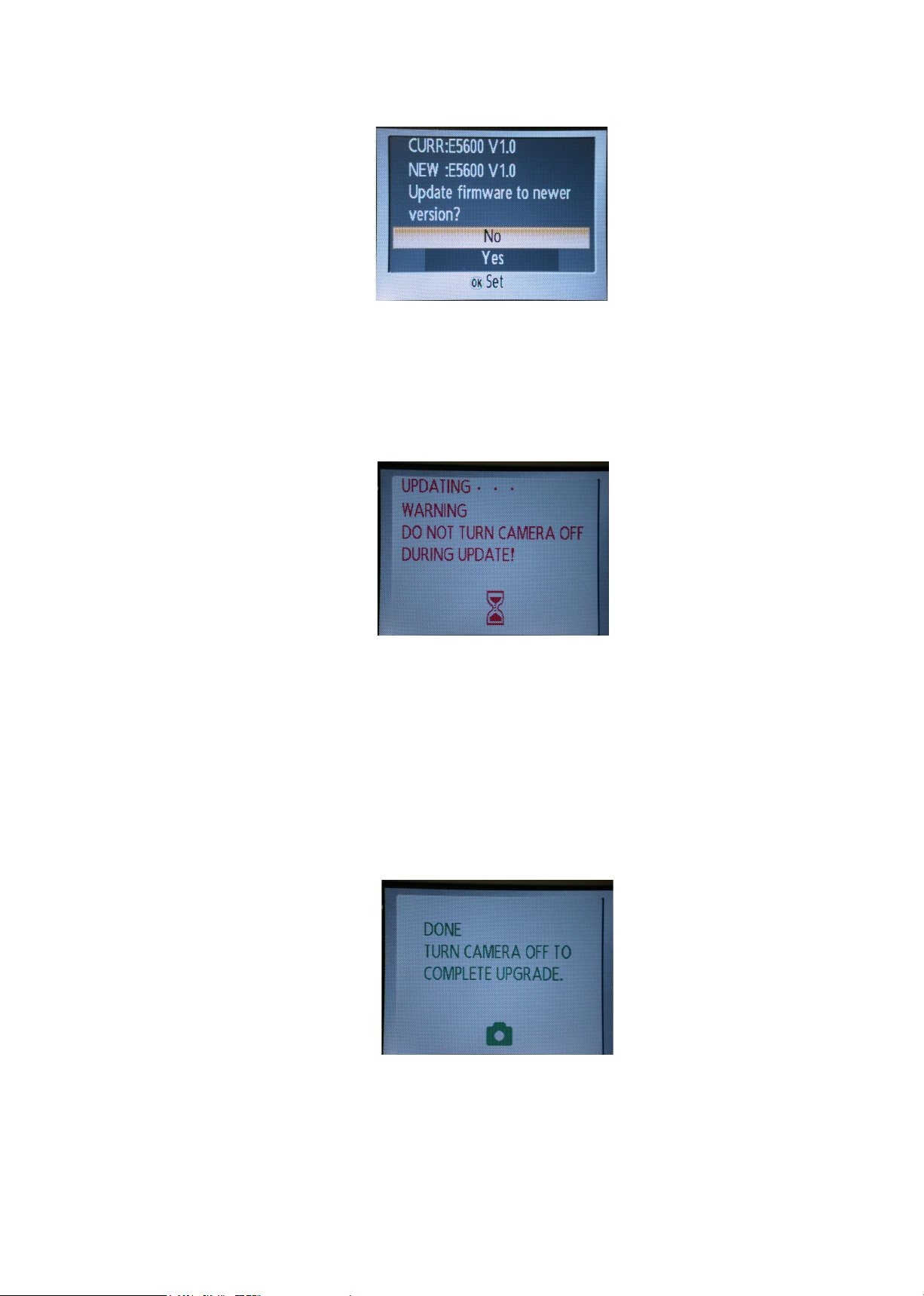
・ When the data writing is completed, the menu for upgrading will be displayed. (Fig.3)
(Fig.3)
・ Select "Yes", and press the decision button to carry out upgrading. (Fig.4)
Note: Do NOT turn power OFF during upgrading.
VAA31001-R.3651.A
(Fig.4)
・ When the screen indicates the completion of upgrading, turn power OFF and remove the SD card. (Fig.5)
・ Turn power ON, and check the version by "Firmware version" on the menu.
・ Turn power OFF to end.
(Fig.5)
- A27 ・ E5600 -
Page 54

5. Setup
1) System requirements
• Windows® 98 or Me, 2000, XP
• IBM-compatible PC/AT with Pentium or higher processor
• CD-ROM drive
• 3.5-inch 2HD diskette drive
• USB port
• 40 MB or more RAM
• Hard disk drive with 15 MB or more memory space
• VGA or SVGA monitor with 256 or more color display
2) Installing calibration software
• Insert the calibration software installation diskette into the diskette drive.
• Open Explorer.
• Copy "DscCalDi.exe, Camapi32.dll" folder of the oppy disk drive in any folder on the hard disk.
VAA31001-R.3651.A
6. Installing USB driver
If the USB driver is necessary, install Nikon View via CD-ROM packed with the camera.
- A28 ・ E5600 -
Page 55
VAA31001-R.3651.A
7. Pattern box
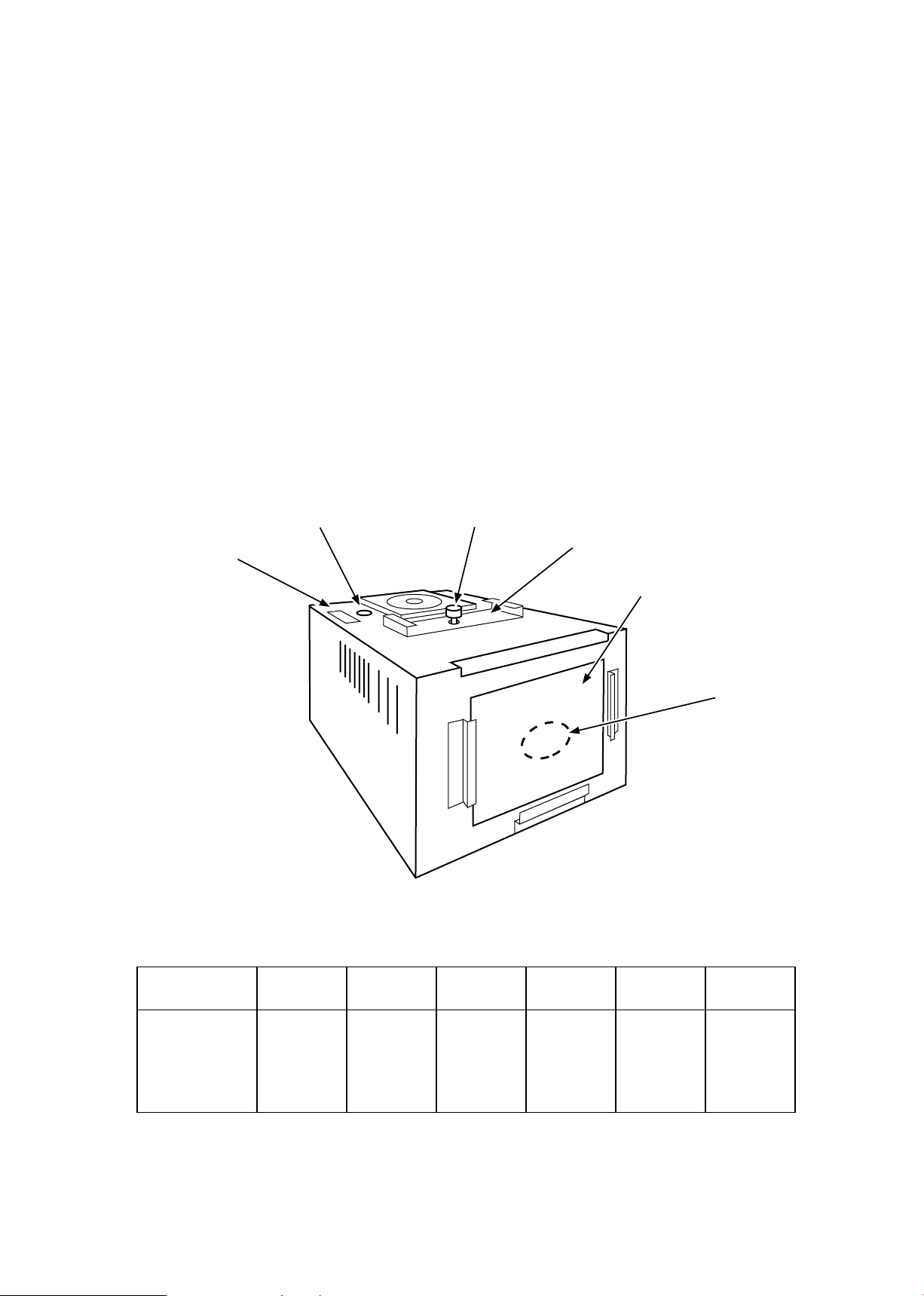
Before using the pattern box, turn its power on to carry out "Aging" approx. 30 minutes: the color temperature should
be 3100 ± 20K by the adjustment with the color meter, and the luminance should be 900 ± 20cd/m2 by the adjustment
with the luminance meter. When using the pattern box and for a while after its power turns off, the lamp and its
surroundings are subject to high temperatures, so care should be taken when handling.
• Procedure for correcting Pattern Box
Note: Be sure to perform the aging correction.
1) Measure the measuring point (center of diffusion plate) with the Color Meter (J63081).
2) Adjust the pattern box so that the color temperature should be 3100 ± 20K by using "VR for adjustment of the color
temperature".
3) Measure the center of the diffusion plate with the Luminance Meter BM-3000 (J63068).
4) Adjust the pattern box so that the luminance should be 900 ± 20cd/m2by using "Knob for luminance adjustment".
5) Repeat from 1) to 4) So that the color temperature should be 3100 ± 20k and luminance should be 900 ± 20cd/m
2
VR for adjustment of
the color temperature
Knob for luminance
adjustment
Power switch
8. Adjustments required when parts are replaced
Iris unit
Diffusion plate
Area to be measured
Lens Adj. AWB CCD
USB FirmwareupInitial image
Defects
Lens Unit ○ ○ ○ × × ×
Optical lter ○ ○ ○ × × ×
CCD ○ ○ ○ × × ×
CP-1 ○ ○ ○ ○ ○ ○
○ Adjustment is necessary. × Adjustment is not necessary.
- A29 ・ E5600 -
data
Page 56
9. Connecting the camera to the computer
USBポートへ
電源はACアダプタEH-62B
から供給してください。
USBケーブル(
UC-E6)
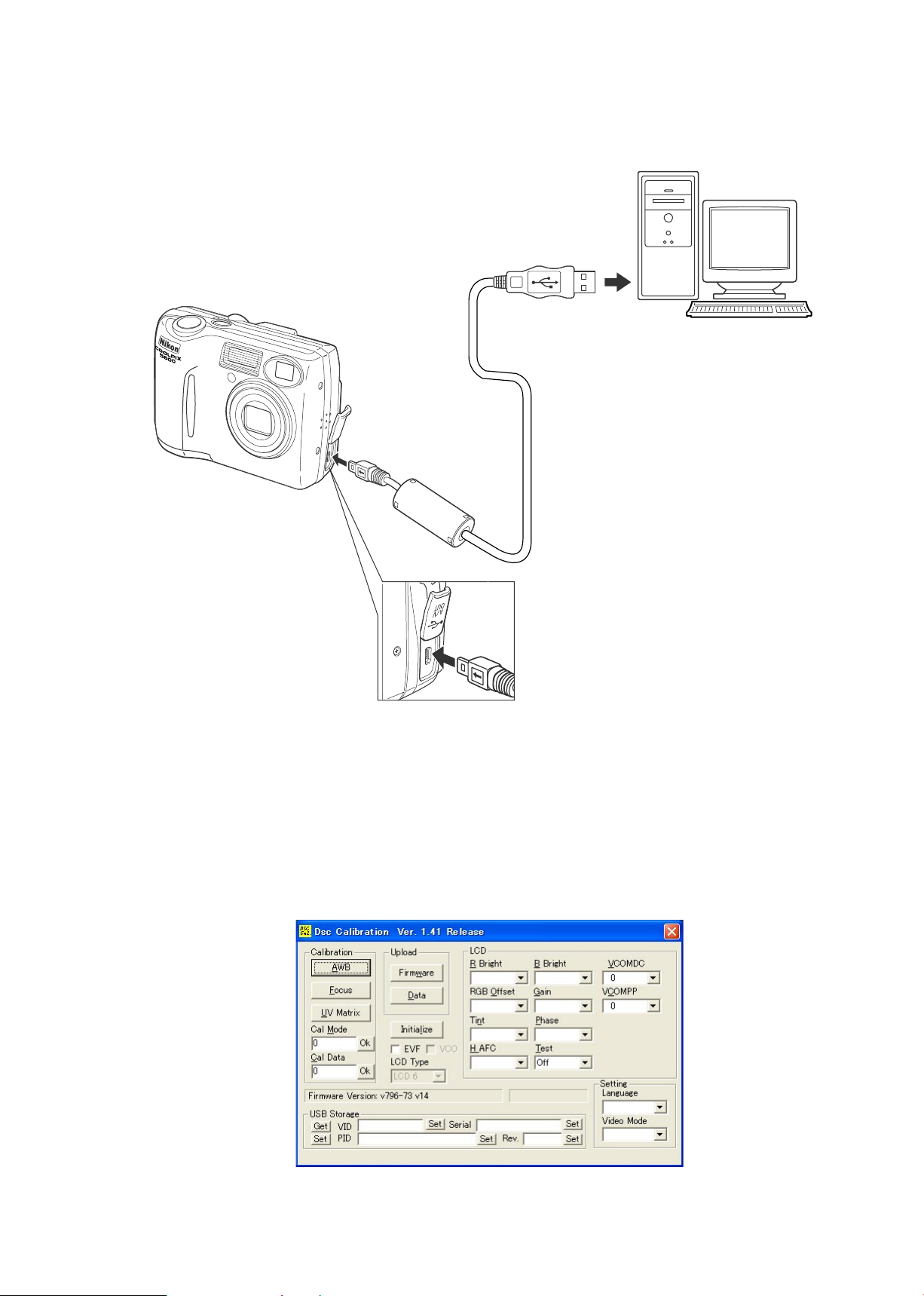
1) Insert the camera connector of USB cable in the notch of the camera’s USB port.
2) Connect the cable to the USB port on PC.
To USB port
USB Cable (UC-E6)
VAA31001-R.3651.A
Supply the power through
the AC adapter (EH-62B).
10. Calibration software
・ Turn on the power switch of the camera.
・ When the calibration software starts, the following is displayed on the PC monitor.
- A30 ・ E5600 -
Page 57
VAA31001-R.3651.A
カメラ
調整用コリメータ
(ジーメンスターチャート内蔵)
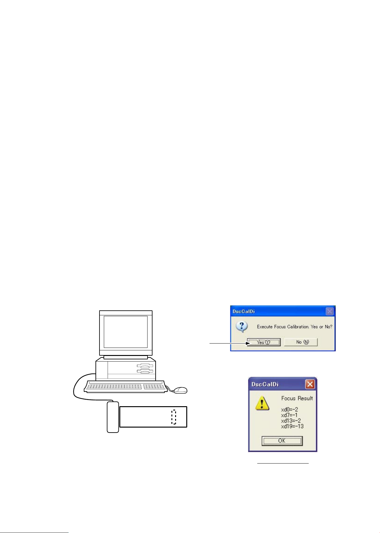
11. Lens adjustment
※ For the lens adjustment, choose either the innity adjustment with the collimator or the 1.5-m adjustment with
the adjustment rmware. (However, in case of 1.5-m adjustment, the focus may not be sharp at innity.)
11-1. Innity adjustment
[Preparations]
• Turn the power switch of the adjustment collimator (C-DSC) J63090 to on.
• Turn the power switch of the camera to on.
• Siemens star chart
• POWER switch of camera: ON
[Conditions]
• Set the adjustment collimator and the camera (front surface of lens) at the nearest distance between them.
[How to]
• Double-click on "DscCa1Di.exe".
• Set the siemens star chart so that it comes center of the screen by checking through the viewnder.
• Click "Focus", then "Yes".
• Lens adjustment value will appear on the screen.
Judgment standard: xd0 = 0 ± 55 , xd7 = 0 ± 55 , xd13 = 0 ± 55, xd19 = 0 ± 55
• Click "OK".
"Yes"
Camera
Adjustment collimator
(Siemens star chart built-in)
Result of adjustment
- A31 ・ E5600 -
Page 58
VAA31001-R.3651.A
カメラ
150cm±3cm
ジーメンス
スターチャート
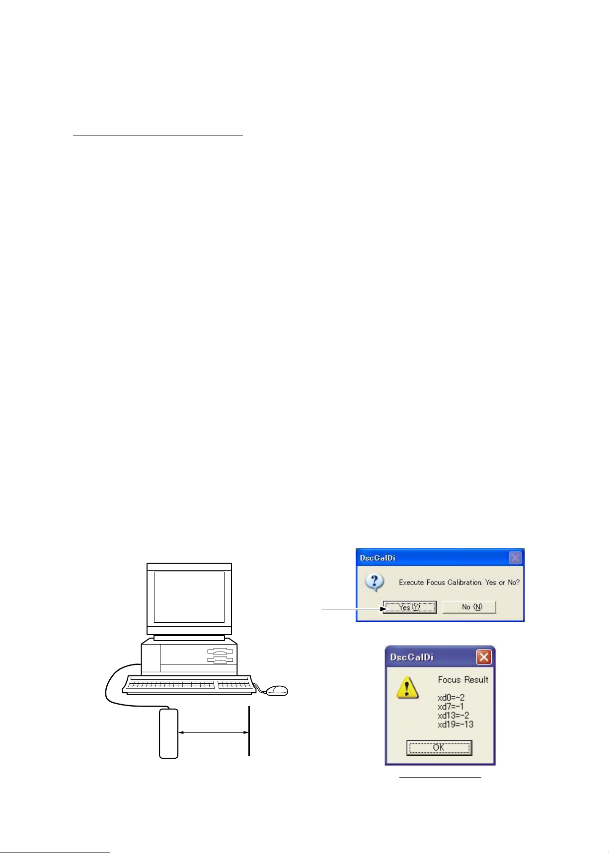
11-2. 1.5-m Adjustment
※ Before performing the 1.5-m adjustment in this machine, write the adjustment rmware on the camera. After
adjustment, be sure to write the product rmware.
Procedure for setting Adjustment rmware
1) Save the adjustment rmware and the product rmware in any folder.
2) Start up "DscCa1Di.exe" and click on "Firmware" button on the main menu to write the adjustment rmware.
(If the camera is activated after completing writing the adjustment rmware, "SERVICE" is indicated in red letters
on LCD panel.)
3) Follow the instructions of the below [How-to].
4) Start "DscCaDi140" and click "Firmware" on the main menu to write the product rmware.
[Preparations]
• Set the Siemens star chart.
• Turn the power switch of the camera to on.
[Conditions]
• The siemens star chart should be A3-size or larger (Copy and enlarge A4-size siemens chart included in the
service manual for the usage.)
• Illumination over the object should be 400 lux ± 10%
• Set the siemens star chart and the camera (front surface of lens) at 150 cm ± 3 cm distance between them.
[How-to]
• Double click on "DscCa1Di.exe".
• Set the siemens star chart so that it comes center of the screen by checking through the viewnder.
• Click "Focus" then "Yes".
• Lens adjustment values will appear on the screen.
Judgment standard: xd0=0 ± 55, xd7 = 0 ± 55, xd13= 0 ± 55 xd19 = 0 ± 55
• Click "OK".
"Yes"
Camera
Siemens star chart
Result of adjustment
- A32 ・ E5600 -
Page 59
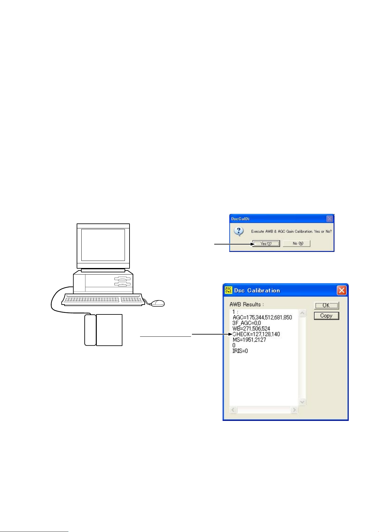
12. AWB adjustment
カメラ
バターンボックス
[Preparations]
• Pattern Box(Color temperature: 3100 ± 20K, Luminance: 900 ± 20cd/m2)
[Conditions]
• Set the pattern box and camera (lens front) at "0cm" distance between them.
Note) Do not allow outside light to enter in.
[How to]
• Double-click on "DscCa1Di.exe".
• Click "AWB", then "Yes".
• AWB adjustment values will appear on the screen.
Judgment standard: CHECK=128 ± 1, 128 ± 1, 130 ± 40
• Click "OK".
VAA31001-R.3651.A
Camera
"Yes"
Result of adjustment
Pattern Box
- A33 ・ E5600 -
Page 60
VAA31001-R.3651.A
- A34 ・ E5600 -
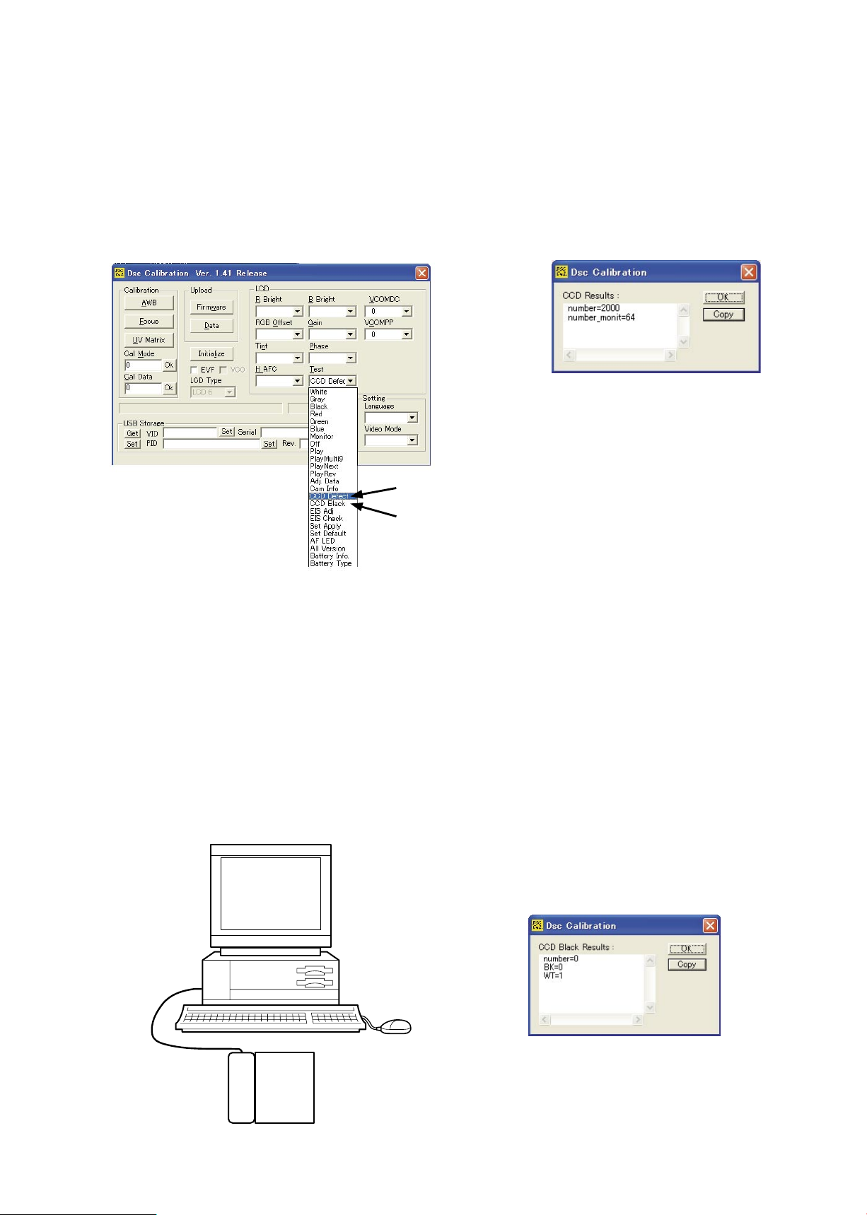
13. CCD white dot defect compensation
[Conditions]
• With the lens shutter being closed, read the defect of CCD pixels. Then, make the correction data and rewrite the
data by the following procedure.
Correct the upper level of defective 2000 pixels from the brightest number of CCD pixels..
[How to]
• Double-click on "DscCa1Di.exe".
• Select "CCD Defect" from Test menu of Calibration Software and click the "OK". Refer to FIG-1.
• After adjustment, the adjustment value will appear on the screen. Refer to FIG-2.
14. CCD black dot/white dot defect adjustment
[Conditions]
• Fix the camera so that only the white part of the pattern box should be displayed on the screen.
(Do not allow outside light to enter in as much as possible.)
• With the lens shutter being opend, read the defect (black dots) of CCD pixels. Then, make the correction data and
rewrite the data by the following procedure.
Correct the upper level of defective 256 pixels (black dots in bright place) of CCD pixels.
[How to]
• Double-click on "DscCa1Di.exe".
• Select "CCD Black" from Test menu of Calibration Software and click "OK". Refer to FIG-1.
• After adjustment, the adjustment value will appear on the screen. Refer to FIG-3.
カメラ
バターンボックス
Pattern Box
Camera
CCD Defect
CCD Black
<FIG-1>
<FIG-2>
(FIG-3)
Page 61
VAA31001-R.3651.A
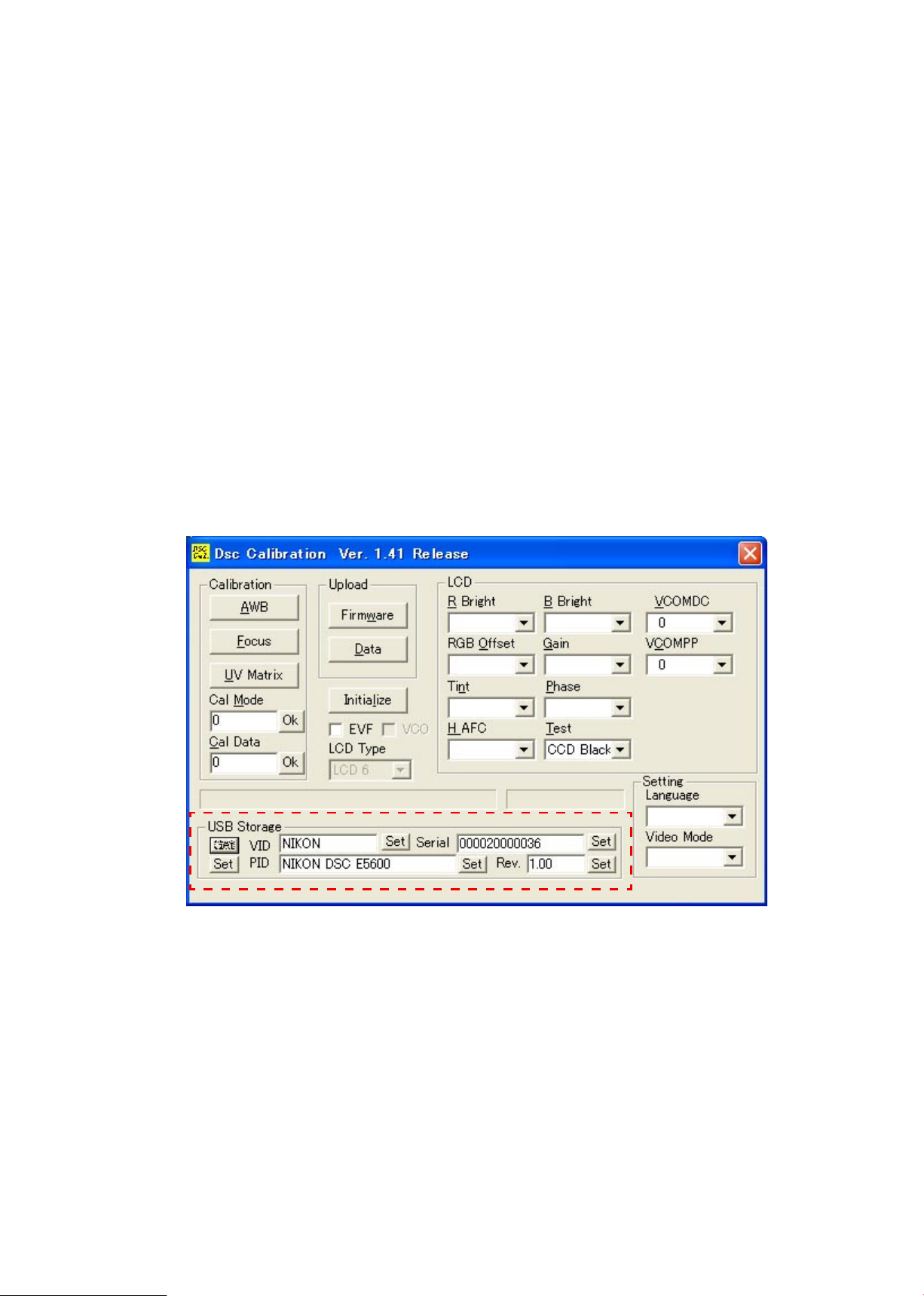
15. USB storage information registration
USB storage data is important when the camera is connected to a computer via a USB connection.
If there are any errors in the USB storage data, or if it has not been saved, the USB specications will not be satised,
so always check and save the USB storage data.
[How to]
• Connect the camera to a computer.
• Double-click on the "DscCa1Di.exe".
• Click on the "Get" button in the USB storage window and check the USB storage data.
VID: NIKON
PID: NIKON DSC E5600
Serial:
Rev. : 1.00
• Check the “Serial” in the above USB storage data. If the displayed value is different from the serial number
printed on the base of the camera, enter the number on the base of the camera, and click the "Set" button.
• Check VID and Rev. entries in the USB storage data. If any of them are different from the values in 3. above,
enter the details of 3. and click the "Set" button.
- A35 ・ E5600 -
Page 62
VAA31001-R.3651.A
- E1・ E5600 -
Page 63
VAA31001-R.3651.A
- E2・ E5600 -
Page 64
VAA31001-R.3651.A
- E3・ E5600 -
Page 65
VAA31001-R.3651.A
- E4・ E5600 -
Page 66
VAA31001-R.3651.A
- E5・ E5600 -
Page 67
VAA31001-R.3651.A
- E6・ E5600 -
Page 68
VAA31001-R.3651.A
- E7・ E5600 -
Page 69
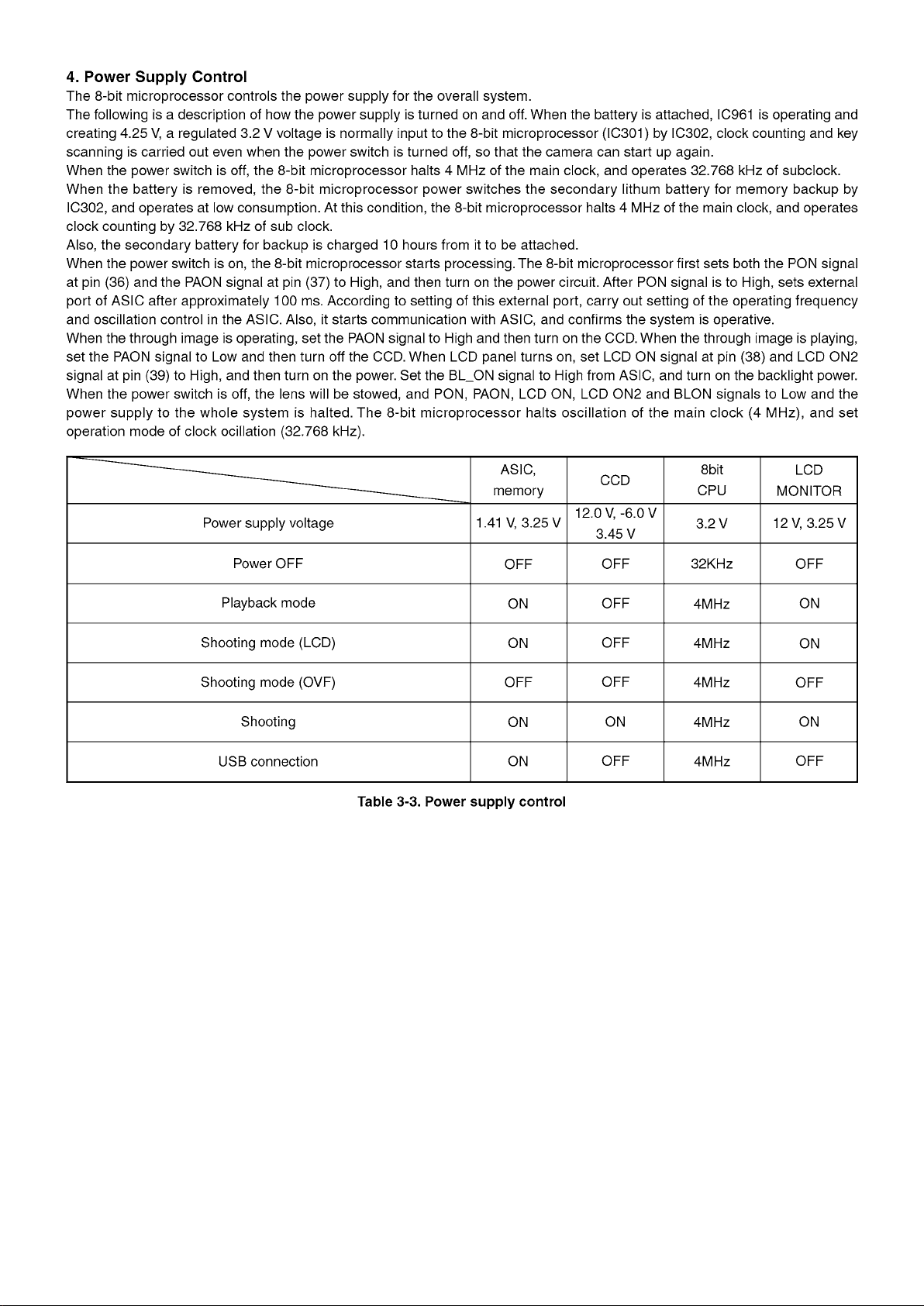
VAA31001-R.3651.A
- E8・ E5600 -
Page 70
VAA31001-R.3651.A
- E9・ E5600 -
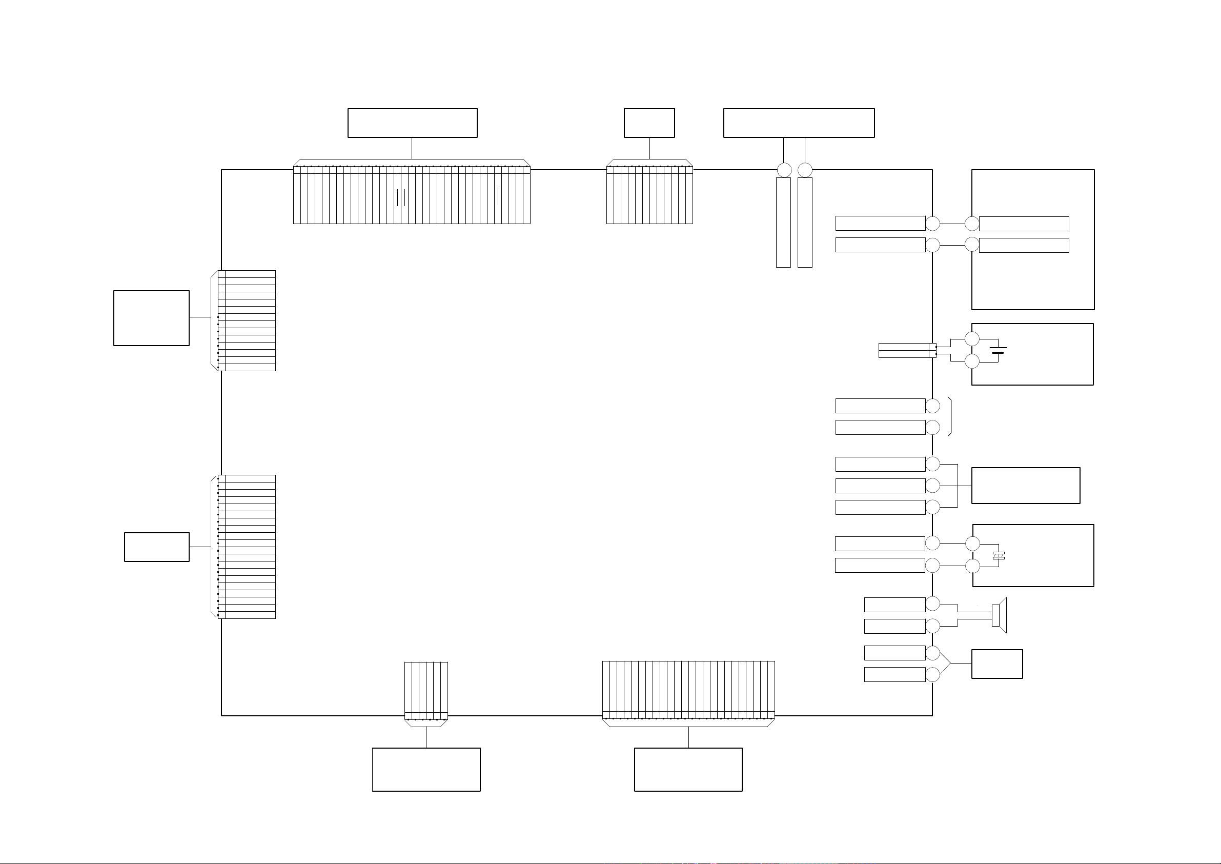
総合結線図
OVERALL WIRING
COMOUT
C1+
VSS
VVCOM
VDC1
COMDC
D01
VSH
D00
VBC
VGH
VDD
C1-
VGL
C2+
C2-
D02
D04
D03
VSYNC
HSYNC
TEST
VCOM
D07
D06
CLK
D05
VSS
BLON
SCK
POCB
CS
DI
CLOCK
CARD/WP
DATA1
DATA2
DATA0
VDD
VSS
CARD
VSS
WP
COMMAND
WHITE
JW601 LED_A
JW602 LED_C
CL308 LED_A
CL307 LED_C
GRAY
DATA3
GND
AUDIO_OUT
USB D(+)
ZAV_JACK
GND
USB D(-)
USB_VDD
VIDEO_OUT
JW502 BAT- (BLACK)
JW501 BAT+ (RED)
GND
BACK UP BAT
FPI E
IRIS+
FPI K
SHUTER-
IRIS-
ZPLS E2
ZPLS K2
SHUTER+
DC 2+
DC 1-
PIV
ZPLS K1
ZPLS E1
SP- (WT)
W1400 XAN (PINK)
W1600 TRG (GRAY)
W1500 XKT (BLUE)
JW541 XAN (LPK)
JW551
+
-
JW552
JW542 GND (BLACK)
PIV
ZPIE
ZPIK
2B
2A
1B
1A
SCAN OUT 4
SCAN IN 0E
AL3.2V
PW_LED
SCAN IN 2E
SCAN IN 1E
SCAN IN 0C
SCAN IN 0D
SCAN IN 4D
SCAN IN 1
AF.LED(G)
SB.LED(R)
SCAN IN 2C
SCAN IN 1C
SCAN IN 3D
SCAN IN 1D
SCAN OUT 3
SCAN IN 2D
SCAN OUT 3
SCAN IN 4C
SCAN OUT 2
SCAN OUT 1
SCAN OUT 0
SCAN IN 3C
SCAN IN 2
SCAN IN 4
SCAN IN 3
SCAN IN 2
SCAN IN 3
AL 3.2V
GND (BK)
SP+ (RD)
MIC (RD)
SPEAKER
TB2
TB1
LCD_AN (RED)
LCD_CA (WHITE)
CP1
GND
-6
-5
GND
GND
-4
GND
-1
-3
GND
-2
GND
LED
BACK UP
ST1
LCD PANEL SD
LCD BACK LIGHT
VIDEO
&
USB
LENS
REFLECTOR
FLASH
MIC
UNIT
RELEASE BACK SW
UNIT
CN110
CN171
CN143
CN303
CN951
CN301
CN302
16151413121110
987654321
3332313029282726252423222120191817
121110
987654321
8
7
6
5
4
3
2
1
2
1
13
12
11
10
9
8
7
6
5
4
3
2
1
20
19
18
17
16
15
14
65432
1
242322212019181716151413121110
987654321
DMA
DMA
DMA
SYA
PWA
SYA
TO BATTERY
PWA
DMA
(DMA)
(SYA)
(CAA)
(PWA)
(STA)
STA
SYA
SYA
DMA
STA
DMA
W1-68900/SX796-JNK
Page 71
VAA31001-R.3651.A
- E10 ・ E5600 -
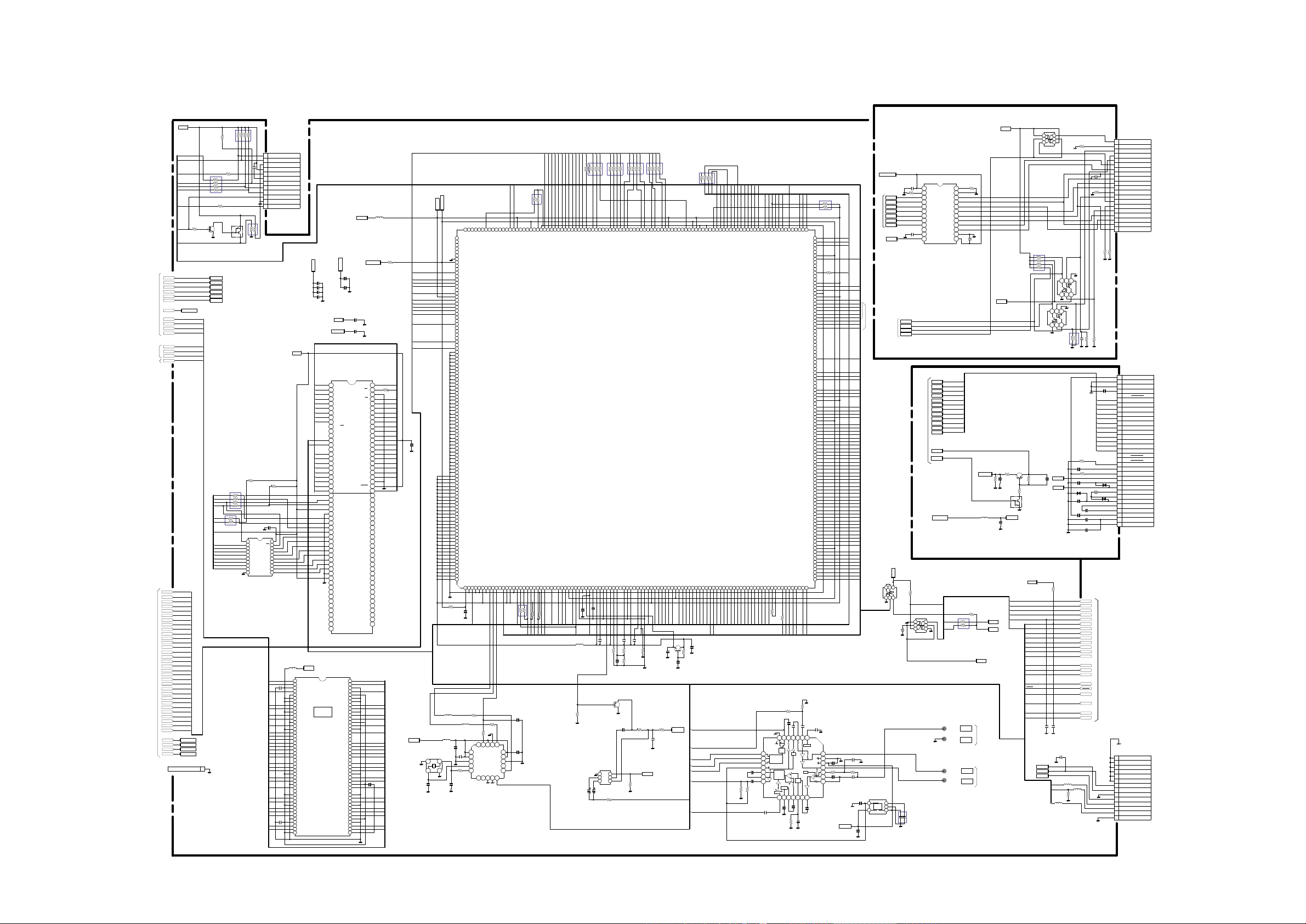
CP1(DMA) 回路図
CP1(DMA)CIRCUIT DIAGRAM
BA0
BA1
DQM0 DQM1
SP+
GND
MIC
DQM2 DQM3
SP-
NAND
SD
398
400
399
395
396
392
393
390
391
394
397
388
389
1
31
IC101
IC101
161 147
373
374
371
372
380
382
381
378
379
387
384
383
386
385
376
375
377
285
241
370
318 281
308
195
234
110153
55 62
A4
A2
A3
A1
A6
A5
A17
A7
REn
A13
A14
A12
A15
R/Bn
A8
WE
NC
NC
NC
A18
RESET
RY/BY
A19
A11
A9
A10
DATA3
COMMAND
DATA1
DATA2
DATA0
CLOCK
CARD
VSS
VSS
VDD
CARD/WP
WP
OE
CE
VSS
A0
DQ8
DQ0
DQ9
DQ1
NC
A16
BYTE
NC
VSS
DQ15/A-1
DQ13
VCC
DQ11
DQ10
DQ2
DQ3
DQ5
DQ4
DQ12
DQ7
DQ6
DQ14
C2-
C2+
VDC1
VGH
VDD
COMDC
VSH
VBC
D01
D00
D02
D03
D04
D05
D06
D07
CLK
HSYNC
VSYNC
SCK
DI
CS
BLON
POCB
TEST
VSS
VCOM
PIV
ZPLS K1
ZPLS K2
ZPLS E1
ZPLS E2
DC 1DC 2+
SHUTER-
SHUTER+
FPI K
IRISIRIS+
FPI E
PIV
ZPIK
ZPIE
2B
2A
1A
1B
VCC
INA
INB
VREF
MD1
IN2
FC
VC
IN1
MD2
EN
ILM
RFG
OUT2
OUT4
OUT6
OUTB
OUTA
OUT5
OUT3
OUT1
GND
VB
GND
SD23/AE13
SD25/AF13
SD24/AB13
SD19/AB14
SD20/AE14
SD15/AE15
SD13/AB15
SD14/AF16
SD17/AF15
SD16/AA15
SD22/AF14
SD21/AA14
SD18/W14
SD12/W15
SD26/W13
SD2/AF19
SD3/AA17
ZCCE2/AE19
SD0/AB18
SD1/W17
SD7/AF18
SD6/AA16
SD11/AE16
SD10/AF17
SD9/AB16
SD8/AE17
CVDD/AE18
SD5/AB17
SD4/W16
GND
GND
GND
GND
GND
GND
GND
GND
OVDDW/VDD
OVDDW/VDD
OVDDW/VDD
OVDDW/VDD
OVDDW/VDD
OVDDW/VDD
OVDDW/VDD
OVDDW/VDD
GND
GND
GND
GND
GND
GND
GND
GND
GND
GND
GND
GND
GND
PPO13/R22
PPO16/T22
PPO19/U21
PPO22/W26
LCD4FSC/W25
PPO23/U19
PPO20/U22
PPO21/V25
PPO17/T19
PPO18/V26
PPO14/T25
PPO15/U26
SPSD/V22
ZSWP/Y26
CVDD/U25
PPO9/R19
PPO8/R21
PPIO4/P21
PPIO7/R26
PPIO5/P25
PPIO6/P22
PPO10/R25
PPO11/T26
PPO12/T21
ASTREQ/B13
VSTDATA5/E15
VSTDATA7/F16
VSTDATA6/B16
VSTDATA1/F14
VSTDATA0/A14
VSTDATA4/A15
VSTDATA2/B14
VSTDATA3/E14
VCTRLEN/A18
VSTREQ/B17
ASTFLG/H15
ASTDATA/A13
PPIOB20/E10
PPIOB21/A9
PPIOB22/F10
PPIOB23/B9
PPIOB17/A8
PPIOB18/H11
PPIOB19/B8
VINCLK/B10
VDATA0/A11
VOUTCLK/F11
VSYNC/A10
CVDD/E11
VDATA7/E13
ASTEN/F13
DP/A16
OVDDW/F15
VSTEN/E16
DM/B15
CVDD/A17
VDATA5/A12
VDATA4/F12
VDATA6/B12
VDATA2/E12
VDATA3/B11
VDATA1/H12
XV2/A23
XV3/A24
XV1/E21
XV6/B24
XV5/F20
DSCK1/L26
DSCK2/M22
DSDO1/K22
ZDSCS0/K26
DSDO2/K25
DSDO0/L21
ZDSCS2/L22
ZDSCS1/M19
DSCK0/L25
SREQ/N19
PPIO2/N26
PPIO3/P26
PPIO0/N22
PPIO1/N25
PPCS/N21
RTS/J22
RXD2/J26
TXD2/J25
CTS/L19
XSG1A/G21
XSG3B/E26
XSG2A/F22
IVDDW/F26
XSG2C/E25
XSG2B/J19
SUBGT/J21
XSG1C/D25
XSG1B/D26
TXD1/H25
BRCK/K21
CVDD/K19
RXD1/H26
XV8/C26
XV7/C25
PBLK/G25
CPDM/H22
CPOB/G26
XSUB/H21
XSG3/F25
HBLK/G22
SCK/M26
SDO/M21
SDI/M25
XV4/B23
BLCK/B21
CCD11/E19
ADCK/A21
CSYNC/A22
TGVD/H18
TGHD/E20
CCD7/A20
CCD5/B19
CCD6/E18
CCD8/H17
CCD2/H16
CCD0/B18
CCD1/E17
CCD4/F17
CCD3/A19
CCD10/F18
CCD9/B20
XVS/F19
XVH/B22
GND
GND
ZMOE/AB20
ZMWE/AA18
GND
GND
GND
GND ZCCE1/AB19
IVDDW/AF20
ZSCE/AE20
ZREG/AF21
CD3/AB26
CD2/W21
CD7/AC26
CD10/AD26
CD12/AE24
CD11/AD25
CD9/AC25
CD8/AA22
CD6/Y21
CD5/AB25
CD4/Y22
CRZB1/AA26
CRZB0/V19
CDT1/Y25
CDT0/V21
CD1/AA25
CD0/W22
ZWAIT/AF22
ZIORD/AE21
ZIOWR/AB21
CA3/W18
CA1/AA19
CD14/AA20
CD13/AF24
CD15/AE23
CA0/AF23
CA2/AE22
PPIOB16/F9
PPIOB14/H10
PPIOB15/E9
IVDDW/B7
GND
GND
GND
GND
GND
PPIOB7/A6
PPIOB1/A4
PPIOB2/B4
PPIOB0/A3
PPIOB6/B5
PPIOB4/A5
PPIOB3/F7
PPIOB5/E6
PPIOB11/E8
PPIOB10/B6
PPIOB13/A7
PPIOB12/H9
PPIOB9/E7
PPIOB8/F8
GND
GND
GND
GND
A1
DIR
G
VCC
B4
A5
B3
A4
A7
B6
GNDA8B8
B7
B5
A6
B1
B2
A2
A3
NC
NC
VSS
IO2
IO1
IO6
IO4
IO5
IO8
IO7
IO3
VCCn
NC
WEn
WPn
VSS
CEn
VCCn
ALE
CLE
NC
NC
NC
NC
NC
NC
NC
NC
NC
NC
NC
NC
NC
NC
NC
NC
NC
NC
NC
NC
VVCOM
COMOUT
C1+
C1-
VGL
VSS
SD31/AB12
SD30/AF12
DQM0/AA12
SD29/W12
SD27/AE12
SD28/AA13
SA3/W10
ZRWE/AE10
CVDD/AB10
SA1/AF10
SA0/W11
SA2/AA11
SA7/AB9
SA9/AB8
SA13/AF7
ZRAS/AF6
SA14/AE6
ZCAS/AB7
SA8/AE8
SA5/AA10
SA4/AE9
SA6/AF9
SA11/AA9
SA10/AF8
DQM1/AE11
DQM3/AF11
DQM2/AB11
SA12/AE7
CKIN2/E2
CKIN1/D1
FSC4/E1
OVDDW/VDD
OVDDW/VDD
OVDDW/VDD
OVDDW/VDD
VDDP/B3
OVDDW/VDD
OVDDW/VDD
PLLSEL0/D2
PLLSEL1/F5
PLLTEST/C1
PLL27M/J8
PLLEN/G6
GNDP/C2
PADDG33/M5
A17/K1
JSEL/L2
A20/L5
A19/M8
A21/J1
CVDD/L6
A18/K2
PADCH1/M6
PADADAVDD/N8
PADVGY/N2
PADYOUT/N5
PADCH0/M2
PADVREFM/M1
PADAGND1/N6
PADVREFH/L1
TEST2/K8
RSTSEL/H5
SCNEN/J5
TEST1/G2
TEST0/G1
TCK/J6
TMS/H2
CLKSEL0/F2
CLKSEL1/F
MCLK/G5
ZRST/H6
TRST/K5
TDI/L8
ZCS1/J2
ZCS0/K6
TDO/H1
OVDDW/VDD
OVDDW/VDD
OVDDW/VDD
OVDDW/VDD
OVDDW/VDD
OVDDW/VDD
OVDDW/VDD
OVDDW/VDD
OVDDW/VDD
OVDDW/VDD
OVDDW/VDD
OVDDW/VDD
OVDDW/VDD
OVDDW/VDD
OVDDW/VDD
OVDDW/VDD
OVDDW/VDD
D4/AB6
D9/AC1
D15/AA2
ZWE/Y1
D14/W6
ZRE/Y5
D11/AB1
D13/AA5
D12/AA1
D10/V8
D7/AB2
D6/AD1
D8/AC2
D5/Y6
RDY/AA7
CKRE/AE5
CKRAM/W9
ZRCE/AA8
DREQ/AE4
DACK/AF5
D2/AE3
D0/AF4
D1/AF3
D3/AD2
PADAGND3/T2
A16/T5
IVDDW/R6
PADVREF/P2
PADDVDD/N1
PADAGND3/R5
PADAVDD/R2
PADUOUT/P6
PADVGUV/P5
PADAOUT/8R
PADVOUT/P1
PADFS/P8
PADVGA/R1
A13/U2
A3/V6
A2/W1
A5/U8
A7/V1
A6/W2
A4/W5
A1/Y2
A9/U6
CVDD/T8
A8/V2
A11/T6
A10/V5
A12/U1
A15/T1
A14/U5
DQ2 DQ13
NC
NC
NC
NC
NC
NC
NC
NC
NC
NC
NC
NC
NC
NC
NC
GND
A11
NC
ZRAS
ZCAS
ZWE
ZCS
A10
VDD
A0
A1
VSSQ
DQ6
VDDQ
DQ1
DQ5
DQ7
VDD
DQ0
VDDQ
VSSQ
DQ4
VDDQ
DQ3
VDD
DQ11
VSSQ
DQ12
VDDQ
VSSQ
DQ15
VSS
VDDQ
DQ10
DQ14
VSSQ
DQ8
CLK
CKE
VSS
VSS
A4
A5
A8
NC
A6
A7
NC
NC
A9
DQ9
GND
GND
PADYOUT
TEST1
XOUT
XIN
CLK1OUT
CLK2ON
FS1
XTAL,SEL
VDD2
TEST2
REFCLK
AVDD
CLK2OUT
VDD1
VSS2
VSS1
AVSS
VDD1
AVDD
CTRL
MUTE
LINE
+42.5dB
0dB
LPF
30K
REG
0dB
0dB
0dB
EVR
LOGIC
SPBIAS
VDDQ
DQ21
DQ22
VDDQ
DQ20
VSSQ
DQ19
DQ23
VSSQ
DQ18
DQ17
VDDQ
VDD
DQ16
A2
NC
DQ24
VSSQ
DQ28
DQ25
VDDQ
DQ26
VSS
DQ31
VDDQ
VSSQ
DQ27
DQ29
VSSQ
DQ30
NC
A3
+6.5dB
+6.5dB
15K
+7dB
LABIAS
ALC
VIDEO_OUT
USB D(+)
AUDIO_OUT
ZAV_JACK
USB_VDD
USB D(-)
GND
GND
NOR
NAND
TOMAIN
TOPWA
TOMAIN
H=0.9
OM/ORFIV024Z
2125
2125
OM/ORBG107W1TOSZ_R
OM/ORZJ11B6390MHBZ
H=0.95
H=0.95
OM/ORZJ11SJ100GZ
OM/ORTR77Z
TOCAA
OM/ORSO20Y1TIZ
H=1.4
H=0.95
H=1.35
H=1.35
OM/ORLL2125Z
OM/ORTR71Z
OM/ORTR71Z
H=0.55
OM/ORBA1005L2Z
OM/RXR71AZ
STBY
GND
H=1.0
GND
GND
-4
-5
-6
GND
GND
-3
OM/ORAT01Z
OM/ORIC20ICSZ
H=1.2
CT3528B2Z
CT2125A2AZ
H=1.2
VCC
VIN
VSAG
VOUT
ON/OFFIN
OUT
H=1.4
OM/ORTR25Z
-1
-2
GND
GND
H=1.4
H=1.4
1608
1608
2125
2125
1608
1608
TO MAIN
OM/ORSO24Y1SANZ_M2
OM/ORTR56Z
OM/ORTR56Z
2125
OM/ORTR56Z
2125
2125
2125
1608
2125
2125
2012
OM/ORLL2125Z
H=0.95
2125
2012
BGA
256M(32)
1608
1608
1608
1608
1608
1608
1608
REG
3.0V
Hi-ON
1608
1608
0.5
TO MAIN
RD
RD
BK
TO MIC
TO SPEAKER
WT
TOCN110
TOCN110
ZWAIT
FD4
FD2
FD1
FD0
FD3
ZCCE1
ZCARDZCARD
PAON2
CDT0
VMONIT
FLCTL
CHG
ZREG
ZIOWR
VDD3
VDD1.41
TOPWA
TOSTA
TOPWA
UNREG
VDD3
BLON
LCDON
BOOST4.25V
-6.0V(A)
+12V(A)
+3.45V(A)
PAON
PON
A_VDD1.41
VDD3
VDD1.41
A_VDD3
A3
A7
A6
A8
A5
A18
A19
A4
VDD3
A2
A16
A14
A15
A20
A9
ZFWR
A11
A13
A12
A10
MRST
LCDVD
LCDHD
A_VDD1.41
VDD3
LCDD01
LCDD00
LCDD02
LCDD05
LCDD04
LCDD03
ZVMUTE
NTZPAL
USBSET
CLK2ON
LCDCLK
A_VDD3
VDD1.41
ZCS0
D8
D1
D0
ZFRD
D3
D11
D2
D9
D10
A1
A17
D6
D12
D4
D13
D5
D15
D14
D7
L12V
L3V
LCDD00
LCDD01
LCDD02
LCDD03
LCDD04
LCDD05
LCDCLK
LCDHD
LCDVD
LCDSCK
LCDSD
LCDEN
LCDON2
VDD3
VDD3
LCDSD
LCDSCK
LCDEN
FLCTL
BLON
BOOST4.25V
USBD+
USBD-
PICTL
VDD3
ZRESET
ZRESET
ZPULSE2
ZPULSE2
ZPULSE1
ZPULSE1
FPI
VDD3
FSIN1
FSMD1
FSMD2
FSIN2
ZMIN1
FSEN
ZMIN2
FSEN
ZRESET
XSG2A
XSUB
XSG3
XSG2B
XSG1A
XSG1B
XV6
XV5
XV4
ZSCE
CRZB1
ZSWP
CCDCK
XV2
XV1
XV3
SD11
SD12
SD10
SD13
SD9
SD8
SD19
SD20
SD16
SD14
SD15
SD18
SD17
SD26
SD23
SD25
SD24
SD21
SD22
SDI
SREQ
SDO
FPI
SCK
ZMIN1
ZMIN2
COMREQ
ZPULSE1
ZPULSE2
FSMD1
CCDSD
AUDSD
CCDEN
AUDCK
AUDLD
SD4
SD0
SD1
ZREG
ZIORD
ZCCE1
SD3
SD2
SD6
SD7
SD5
FD5
FD6
FD2
FD3
FD0
FD1
CDT0
FSIN1
FSIN2
PICTL
FD4
FSMD2
CA0
ZWAIT
ZIOWR
FD7
AD9
AD8
AD11
AD10
AD4
AD6
AD5
AD0
AD1
AD3
AD2
AD7
TGVD
TGHD
SUBGT
ADCK
L3V
LCDSCK
LCDD02
LCDD00
LCDD01
LCDVD
LCDD05
LCDHD
LCDEN
LCDCLK
LCDSD
LCDD03
LCDD04
ZSWP
CRZB1
CA0
ZSCE
ZIORD
FD6
FD7
FD0
FD3
FD4
FD1
FD2
FD5
ADCK
+12V(L)
SA7
SA8
SA4
SA3
SA6
SA5
SA11
SA9
SA10
DQM2
SD31
SD28
SD27
SD30
SD29
DQM1
DQM0
SA0
ZRWE
SA2
SA1
DQM3
L12V
VDD3
VDD3
AD10
AD11
XSG3
CCDEN
XV6
TGVD
CCDSD
CCDCK
XV5
TGHD
AD0
AD1
AD2
AD4
AD7
AD5
AD9
AD6
AD8
AD3
VDD3
SD2
SD0 SD15
SD13
USBSET
ASICAIN
CLK2ON
USBDET
USBCNT
USBD+
USBD-
A4A2A1A3A7
A11
A12
A10
A15
A14
ASICAOUT
A16
A13
A8A9A5
A6
D13
D14
D10
D6
D7
ZCAS
ZRCS
ZRAS
SA12
SA13
D1D2D0D4D3
CKRE
CKRAM
D5D9D8
D12
D11
ZFRD
ZFWR
D15
MRST
PLLEN
TDO
TDI
TRST
JSEL
SCNEN
TMS
TCK
A20
A19
ZCS0
A17
A18
ZTEST
USB+
USB-
ZAVJACK
USBCNT
PAON
PON
SDI
SREQ
SDO
MRST
ZTEST
ZCARD
VMONIT
CHG
PLLEN
UNREG
LCDON
COMREQ
SCK
XSG2B
XSG1B
XSUB
XV4
XV3
XSG2A
SUBGT
XSG1A
XV1
XV2
+3.45V(A)
+12V(A)
VDD3
-6.0V(A)
SA12
ZRCS
ZRAS
SA11
SA13
SA0
SA10
SA1
SD4
SD6
SD5
DQM0
ZCAS
ZRWE
SD7
SD3
SD1
VDD3
SA8
SA7
SA5
SA4
SA9
CKRE
CKRAM
SA6
SD14
SD12
SD8
DQM1
SD10
SD9
SD11
AUDLD
AUDCK
AUDSD
VDD3
BEEP
AUDIOOUT
ZVMUTE
PAON2
BEEP
LCDON2
VDD3
BOOST4.25V
USB+
USB-
USBDET
DQM2
SA2
SD22
SD20
SD19
SD21
SD23
SD18
SD17
SD16
SA3
SD25
SD28
SD30
SD27
SD24
SD26
SD31
SD29
DQM3
VOUT
NTZPAL
NTZPAL
ASICAIN
ASICAOUT
VDD3
VOUT
AUDIOOUT
ZAVJACK
E
C
B
M-GND
M-GND
M-GND
M-GND
B
C
E
E
C
B
B
C
E
R1402
R1434
RB145
RB141
C1401
RB142
Q1432
R1404
RB143
Q1431
R1431
R1401
C1007
C1903
C1901
C1018
C1006
C1005
C1020
C1004
R1410
IC121
CN143
L1001
R1001
R1201
C1201
R1734
CN951
R1701
C1701
C9507
R9505
C9501
Q9509
C9502
R9501
C1708
IC101
D1702
C1705
D1703
C1734
C1702
C1703
R1702
D1701
R9509
R9506
R9507
R1003
RB102
R9503
R9504
R9502
C9503
Q9501
RB951
Q9502
RB952
IC951
C9506
RB105
RB108
RB103
RB101
RB106
R1018
RB104
Q1735
R1736
R1735
R1739
C1736
IC143
RB144
C1405
C1709
CN171
C1707
C1704
C1706
L1735
TOPWA
Q1736
C1751
Q1305
R1902
C1083
IC103
L1080
R1002
L1051
C1001
C1057
Q1051
C1050
R1057
C1058
R1302
C1054
C1056
C1059
R1053
C1052
R1093
R1052
R1054
R1005
R1047
RB107
C1002
R1066
C1051
R1064
R1311
Q1301
C1301
RB132
CN191
L1102
X1101
C1104
L1101
C1807
C1825
Q1505
C1519
R1509
R1503
C1504
R1102
R1104
R1103
L1103
C1103
R1111
C1101
C1114
R1815
C1829
C1831
IC152
R1502
IC181
C1828
R1814
C1820
R1813
R1806
C1827
C1810
C1806
C1905
C1904
VA134
C1086
C1102
C1105
C1084
C1823
IC111
C1822
CB181
C1513
C1512
R1501
R1526
C1826
C1824
R1801
R1811
C1821
C1830
IC182
C1815
C1803
R1812
CN110
L1304
R1301
L1302
L1303
100;1/16J
100;1/16J
100
10K
0.1;B
10K
DTA144EM
2.7K;1/16J
100
2SC5658-R
120K;1/16J
10K;1/16J
0.1;B
4.7;B
4.7;B
1;B
1;B
1;B
0.1;B
1;B
10K;1/16J
TV00047002AAGD00GA
12
BK1608LL241-T
0;1/16Z
10;1/16J
1;B
75;1/10J
20
560K;1/16J
10;B
0.1;B
1.3K;1/16D
0.01;B
NSBA123JD
1;B
0.56;1/4F
0.1;B
KS654U2250CBP
RB521S-30
1;B
RB521S-30
1;B
1;B
4.7;B
10K;1/16D
RB521S-30
390;1/16J
47K;1/16J
47K;1/16J
1K;1/16J
10K
390;1/16J
390;1/16J
390;1/16J
0.1;F
EMH16
47K
EMH16
33K
LB8655T-E
0.1;F
220
220
220
220
100
68;1/16J
10K
T12A01SS-TL-E
100K;1/16J
10K;1/16J
47K;1/16J
1;B
SN74LV245A
100
0.1;F
10;B
33
10;B
4.7;B
1;B
LBR2012T470M
10K;1/16J
DTC144EM
4.7;B
EMD3
10K;1/16J
TV00047002AAGD00GA
EDS2532AABH-75
BK1005LL241-T
0;1/16Z
LBR2012T470M
330P;B
1;B
2SC5658-R
0.22;B
3.9K;1/16D
1;B
0.1;F
0.1;B
0.1;B
1K;1/16D
1;B
750;1/16D
3.6K;1/16D
2.2K;1/16D
10K;1/16J
10;1/16J
47K
0.1;B
1K;1/16J
0.1;B
10K;1/16J
1.5K;1/16J
EMH2
1;B
27;D
0.1;B
BK1005LL680
28.63636MHZ
0.01;B
BK1608LL241-T
0.1;B
0.1;B
2SA1774
1;B
1.5K;1/16J
0;1/16Z
0.1;B
100;1/16J
47;1/16J
47;1/16J
BK1005LL241-T
1;B
470;1/16J
0.01;B
10P;CH
2K;1/16D
4.7;B
BH76106HFV
200;1/16D
BH6412KN
0.1;B
200;1/16J
0.1;B
3.9K;1/16D
180K;1/16D
1;B
0.1;B
1000P;B
1000P;B
AVR-M1608C120MT
1;B
5P;CH
5P;CH
1;B
4.7;B
ICS425KLFT
0.1;B
0.022;B
1;B
47;6.3-T
22;4-T
22K;1/16J
75;1/16D
4.7;B
4.7;B
27K;1/16D
39K;1/16D
0.1;B
1;B
MM1613LNLE
1;B
4.7;B
470K;1/16J
0.022;B
21
BK1608LM751
220K;1/16J
BK1608LM751
BK1608LM751
TO SD
TO LCD
SX7MS
TO USB&VIDEO
SDRAM
CLOCK GENERATOR
REGULATOR
QAG68900796CN
1AV4J11B6390M
1AV4J11SL203G
TNSBA123JD--H
QXXAG54U2250N
QLB8655T-E--P
QSN74LV245A-P
1AV4J11VE330G
QEDS2532AAB7N
1AV4J30B1081G
1AV4V10B5620G
QBH76106HFV-G
QBH6412KN---P
QICS425KLFT-J
QMM1613LNLE-G
1AV4J11B5670G
PAON2
VMONIT
FLCTL
CHG
VDD1.41
BOOST4.25V
VDD3
-6.0V(A)
+12V(A)
LCDON
PAON
PON
BLON
+3.45V(A)
UNREG
ADCK
AD10
AD11
XV5
XV6
CCDCK
TGVD
CCDSD
CCDEN
XSG3
TGHD
AD1
AD0
AD6
AD7
AD3
AD4
AD2
AD5
AD9
AD8
SDI
SREQ
SDO
SCK
MRST
COMREQ
ZTEST
ZCARD
UNREG
CHG
VMONIT
LCDON
PLLEN
PAON
PON
ZAVJACK
USBCNT
XV3
XSUB
XSG1A
XSG2A
SUBGT
XV2
XSG1B
XV1
XSG2B
-6.0V(A)
VDD3
+12V(A)
+3.45V(A)
PAON2
LCDON2
BEEP
BOOST4.25V
VDD3
12
11
10
9
8
7
6
5
4
3
2
1
1
2
3
4
5
6
7
8
9
10
11
12
13
14
15
16
17
18
19
20
21
22
23
24
49
50
48
47
46
45
44
43
42
41
40
39
38
37
36
35
34
33
32
31
30
29
28
27
26
25
79
80
20
19
18
17
16
15
14
13
12
11
10
9
8
7
6
5
4
3
2
1
33
32
31
30
29
28
27
26
25
24
23
22
21
20
19
18
17
16
15
14
13
12
11
10
9
8
7
6
5432
1
377
376
375
374
373
372
371
370
369
368
367
366
365
364
363
362
361
360
359
358
357
356
355
354
353
352
351
350
349
348
347
346
345
344
343
342
341
340
339
338
337
336
335
334
333
332
331
330
329
328
327
326
325
324
323
322
321
320
319
318
317
316
315
314
313
312
311
310
309
308
307
306
305
304
303
302
301
300 299 298 297 296 295 294 293 292 291 290 289 288 287 286 285 284 283 282 281 280 279 278 277 276 275 274 273 272 271 270 269 268 267 266 265 264 263 262 261 260 259 258 257 256 255 254 253 252 251 250 249 248 247 246 245 244 243 242 241 240 239 238 237 236 235 234 233 232 231 230 229 228 227 226 225 224 223 222 221 220 219 218 217 216 215 214 213 212 211 210 209 208 207 206 205 204 203 202 201
200
199
198
197
196
195
194
193
192
191
190
189
188
187
186
185
184
183
182
181
180
179
178
177
176
175
174
173
172
171
170
169
168
167
166
165
164
163
162
161
160
159
158
157
156
155
154
153
152
151
150
149
148
147
146
145
144
143
142
141
140
139
138
137
136
135
134
133
132
131
130
129
128
127
126
125
124
654
3 2 1
654
3 2 1
24
23
22
21
20
19
18
17
16
15
14
1312
11
10
9
8
7
6
5
4
3
2
1
10
9
8
7
6
5
4
3
2
1 20
19
18
17
16
15
14
13
12
11
51
52
53
54
55
56
57
58
59
60
61
62
63
64
65
66
67
68
69
70
81
82
83
84
85
86
87
88
89
90
91
92
93
94
95
96
97
98
99
100
6
5
4
3
2
1
400
399
398
397
396
395
394
393
392
391
390
389
388
387
386
385
384
383
382
381
380
379
378 123
122
121
120
119
118
117
116
115
114
113
112
111
110
109
108
107
106
105
104
103
102
101
100999897969594939291908988878685848382818079787776757473727170696867666564636261605958575655545352515049484746454443424140393837363534333231302928272625242322212019181716151413121110987654321
6 5 4
78
901
71
72
73
74
75
76
77
101
102
103
104
105
106
107
321
6
5
4 3
2
1
1
89
88
87
86
85
84
83
82
81
80
79
78
77
76
75
74
73
72
71
70
69
68
67
66
65
64
6328
27
26
25
24
23
22
21
20
19
18
17
16
15
14
13
12
11
10
9
8
7
6
5
4
3
2
3
1 2
4
20 19 18 17 16
12345
1514131211
61
28
27
26
25
2412
11
10
9
8
7 6 5 4 3 2 1
62
61
60
59
58
57
56
55
54
53
52
51
50
49
48
47
4645
44
43
42
41
40
39
38
37
36
35
34
33
32
31
30
29
109876
5432
23
22
21201918171615
14
13
5
4 3
2
1
8
7
6
5
4
3
2
1
LENS DRIVER
TRANSCEIVER
PROGRAM FLASH
VIDEO AMP
TO LENS
XV4
D1-68900/SX796-JNK
DMA(MAIN)
ASIC
DMA(LCD)
DMA(LENS)
TO SYA
AUDIO
Page 72
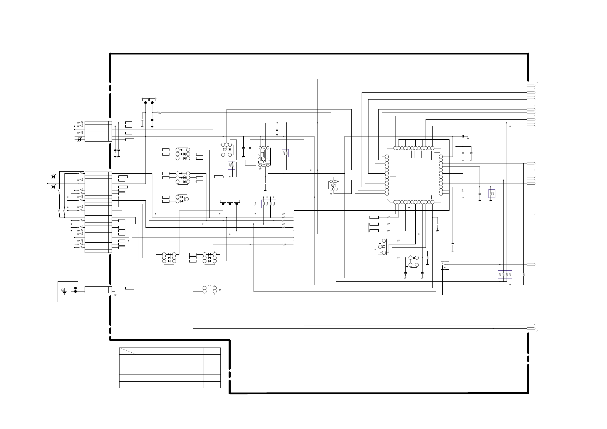
VAA31001-R.3651.A
- E11 ・ E5600 -
CP1(SYA) 回路図
CP1(SYA) CIRCUIT DIAGRAM
ALWAYS3.2V
SW3.2V
OK
DOWN
RIGHT
UP
PW_ON
1st
2nd
SCAN OUT 4
SCAN IN 0E
SCAN IN 2E
AL3.2V
SCAN IN 1E
PW_LED
MOVIE
AUTO
SET UP
NIGHT VIEW
SCAN IN 2
SCAN OUT 1
SCAN IN 3
SCAN IN 2
SCAN IN 0C
SCAN IN 4D
AF.LED(G)
AL 3.2V
SCAN IN 0D
SB.LED(R)
SCAN IN 1
SCAN IN4/TCLK
SCAN IN3/TDO
MMOD
SB.LED(R)
SCAN IN1
AF.LED(G)
SCAN IN0
PA ON2
CHG ON
PA ON
LCD ON
PLLEN
SCAN IN2
P ON
AVREF ON
LCD ON2
BACKUP_CTL
SELF LED
COMREQ/BOT
ASIC TEST
PW_LED
MAIN RESET
XCOUT
VSS
XIN
VDD
XCIN
XOUT
SCAN OUT1
BEEP
SREQ
SCAN OUT0
SCAN OUT4
SCAN OUT2
SCAN OUT3
AVREF
RESET
SI
SO
SCK
VDD
CARD
BAT_OFF
VMONIT
USB_CONNECT
BATTERY
TEMP_BAT
SPORTS
LANDSCAPE
SCENE
PORT
SCAN OUT 3
SCAN IN 3D
SCAN IN 1D
SCAN OUT 3
SCAN IN 2C
SCAN IN 1C
SCAN IN 3C
SCAN OUT 2
SCAN IN 4C
SCAN IN 4
SCAN OUT 0
SCAN IN 3
SCAN IN 2D
SCAN OUT
SCAN IN
BACK UP BAT
GND
1 20 3 4
1
0
2
4
3
PW_TEST
SCENEAUTO
MOVIETEST SET UP
PORTRAIT
2nd1stPW_ON
DEL TELE
NIGHT VIEW
WIDEPLAY
LEFT
RIGHT
UP
DOWN
SPORTS
OK
--
LANDSCAPE
AV JACK
MENU
2125
VDD
OUT
NC
VSS
NC
BACK UP3.2V
OM/ORZJ11SJ060GZ
CL308 CL307
TO TB1
JW601, 602
CT2125PZ_DM
H=1.2
MENU
LEFT
PLAY
OM/ORZJ11SJ240GZ
UNREG
REG.
ALWAYS
3.2V
DET
+LI
ALWAYS
REST
2.4V
GND
OM/ORBA1005L2Z
BATTERY
2.9V
DET 3.3V
DET
OM/ORTR58Z
H=0.55
BACKUP
CL301 CL302 CL303
H=0.6
OM/RTR56Z_DM
DEL
OM/ORXR72Z
OM/ORXF19Z
H=1.2
OM/ORSK02V052AZ
H=1.1
OM/ORIC04SKDAZ
TB2
WIDE
TELE
SI2E
SI1E
SI0E
PW_LED
PAON2
COMREQ
PLLEN
ZTEST
SREQ
USBCNT
PON
LCDON2
LCDON
PAON
CHG
BEEP
SI0C
SI4D
SI0D
AF.LED(G)
SB.LED(R)
SI1C
SI1D SI0C
SI0D
SI2C
SI2D SI3C
SI3D
SI4C
SI4D
BACKUPBAT
SDO
ZCARD
VMONIT
SO0
SO1
SO2
SO3
SO4
SI0
SI1
SI2
SCK
SDI
SI4
SI3
SI4C
SI1D
SI2D
SI3D
SI2C
SI1C
SI3C
SI0E
SI2E
SI1E
SO4
SO3
SO2
SO1
SO0
MRST
SI0
SI1
SI2
SI4
SI3
ZAVJACK
SB.LED(R)
AF.LED(G)
PW_LED
TO CN301
TO CN302
BACKUPBAT
BOOST4.25V
UNREG
CN301
C3001
VA308
R3014
C3007
C3006
CN302
VA303
VA304
D3002
D3001
D3003
RB306
RB302
C3005
IC302
Q3002
R3003
RB305
C3002
C3003
VA302
R3006
Q3001
RB307
IC301
C3016
C3011
D3004D3005
R3017
R3015
C3014
Q3003
R3021
C3015
X3002
RB303
R3018
RB301
R3016
R3019
R3020
R3011
C3008
X3001
C3013
R3013
CN303
IC304
RESET
6
1;B
LED_A
WHITE
LED_C
GRAY
AVR-M1005C080MT
220;1/16J
15;6.3-T
0.1;F
24
AVR-M1005C080MT
AVR-M1005C080MT
NSDEMP11XV6T5
NSDEMP11XV6T5
DAP222
1K
33K
0.1;F
NJU7286ARB
EML17
33K;1/16J
10K
1;B
0.1;F
AVR-M1005C080MT
10K;1/16J
NSBC114EPD
150K;D
MN101C78A-SB1
1;B
1;B
DMA6S121DMA6S121
100;1/16J
150;1/16J
15P;CH
DTC144EM
220;1/16J
20P;CH
32.768KHz-T
1K
1K;1/16J
10K
10K;1/16J
0;1/16Z
220;1/16J
1;B
4M00G55
0.1;B
330K;1/16J
2
XC61CN1502N
33K;1/16J
TO RELEASE UNIT
TO BACK SW UNIT
TO TB2 BACK UP
1AV4J11SJ062G
1AV4J11SJ242G
QNJU7286ARB1G
TEML17------G
QXXAG1C78AB1N
1AV4V10B6900G
1AV4J10QL022G
QXC61CN1502NP
6
5
4
3
2
1
11
10
9
8
7
6
5
4
3
2
1
4
6
3
215
3
2
146
5
1
3
2
8 7 6 5
4321
54
3 2 1
6 5 4
321
48
47
46
45
44
43
42
41
40
39
38
37
36 35 34 33 32 31 30 29 28 27 26 25
24
23
22
21
20
19
18
17
16
15
14
13
121110987654321
24
23
22
21
20
19
18
17
16
15
14
13
12
5
6
44
6
52
1
3 3
1
2
41
2
3
1
2
3
2
1
2
1 4
3
8bit MICRO PROCESSOR
TO DMA(MAIN)
!
Y1-68900/SX796-JNK
SYA
Page 73
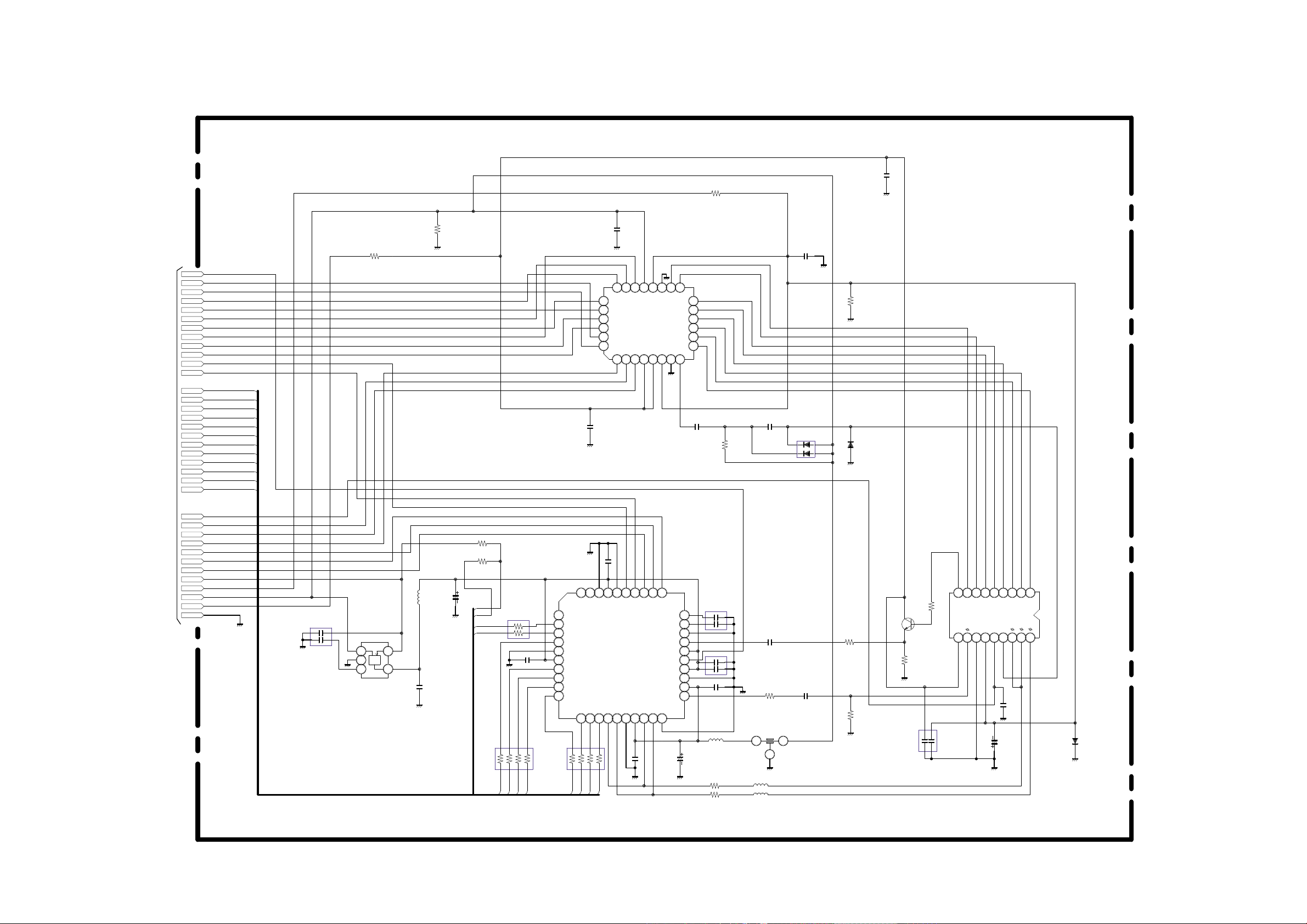
VAA31001-R.3651.A
- E12 ・ E5600 -
CP1(CAA) 回路図
CP1(CAA) CIRCUIT DIAGRAM
CH1
IV3
CH2
VDC
IV1
0V2
VL
VM
0V1
0V3
CH3
IV4
IV2
0V7
0V8
0V5
0V4
IV5
CH5
CH4VHISUB
IV6
VHH
VM
0V6
0SUB
VL
D1
D0
DRVSS
DRVDD
CLP/BLK
HBLK
D3
D2
D6
D5
D8
D7
D4 CCDIN
RGVDD
TCVDD
TCVSS
CL1
AVDD
REFB
AVSS
REFT
DVDD
DVSS
SCK
SDI
SL
HD
VD
RG
VOOD
RG
PWPTSUBSW
SUB
HL
H1
H2
V2
V1
V5B
V6
V3B
V3A
V5A
V4
D9
D10
D11(MSB)
H1
H2
H3
RGVSS
H4
HVSS
HVDD
ON/
OFF IN
REG
3.0V
VOUT
+12V(A)
-6.0V(A)
+3.45V(A)
XV6
XV5
XV3
XSG3
XV1
XSG1B
XSG1A
AD6
AD11
AD7
AD10
AD8
AD9
AD2
AD3
AD1
AD4
AD0
AD5
SUBGT
TGHD
CCDEN
XSG2B
XSUB
XSG2A
TGVD
ADCK
XV2
XV4
VDD3
AD1
AD0
AD2
AD3
CCDCK
CCDSD
+3V
AD8
AD9
AD5
AD6
AD4
AD7
AD11
AD10
E
C
B
R9001
R9004
C9014
IC901
R9007
C9028
R9013
C9026
C9010
C9018
R9008
C9024
D9001
D9003
L9001
C9005
IC904
CB901
C9008
R9018
R9019
RB902
C9012
C9009
R9010
CB903
CB902
IC905
C9023
C9025
Q9001
R9003
R9015
R9016
IC903
C9027
RB903
RB901
L9003
L9004
R9005
C9017
XF901
C9013
L9002
R9006
C9035
D9004
R9014
C9036
CB904
0;1/16Z
470;1/16J
1;B
AN20101A
3.3;1/16J
1;B
82K;1/16J
1;B
1;B
1;H
100K;1/16J
0.033;B
MA4S111
MA2J727
BK1608LL241-T
1;B
TK11130CS
1;B
10;6.3-T
0;1/16Z
0;1/16Z
100
0.1;B
47;1/16J
0.1;B
1;B
AD9948
0.1;B
1000P;B
0.15;B
2SC5661-P
0;1/16Z
1.2K;1/16D
47;1/16D
MN39620
0.01;B
100
100
BLM15BB100
BLM15BB100
15;1/16J
22;10-T
CKD610JB0J225M
1000P;B
BK1608LL241-T
15;1/16J
10;16-T
MA2J727
1M;1/16J
0.1;B
1;B
QAN20101A---P
QTK11130CS--J
XV6
XSG1A
XV3
XV1
XSG3
XSG1B
XV5
ADCK
TGVD
TGHD
XV2
XV4
AD6
SUBGT
AD9
AD10
AD11
AD7
AD8
AD0
AD1
AD2
AD3
AD4
AD5
VDD3
+3.45V(A)
GND
+12V(A)
-6.0V(A)
XSUB
CCDSD
CCDCK
CCDEN
XSG2B
XSG2A
27 26 25 24 23
1413121110
22 21 20 19 18 17 16 15
28
9
87654321
5
43
2
1
40 39 38
10
9
8
7
6
5
4
3
2
1
37 36 35 34 33 32 31
30
29
28
27
26
25
24
23
22
21
10 11 12 13 14 15 16 17 18
9 8 7 6 5 4 3 2 1
131211
1 3
2
20191817161514
V. DRIVER
CDS, AGC, A/D C
H. DRIVER
CCD
TO DMA(MAIN)
C1-68900/SX796-JNK
CAA
Page 74
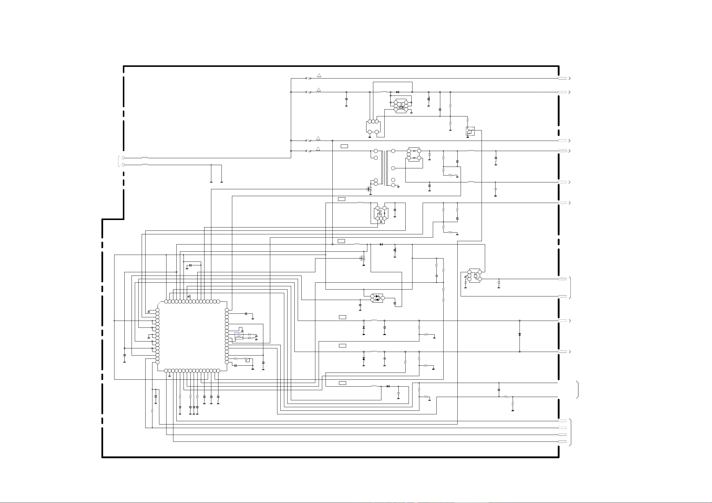
VAA31001-R.3651.A
- E13 ・ E5600 -
CP1(PWA) 回路図
CP1(PWA) CIRCUIT DIAGRAM
WT
TO LCD BACK LIGHT
RD
BAT-
TO BATTERY
JW502
JW501
BAT+
RED
BLACK
<BOOST/LENS>
SWIN6
UDSEL1
SWOUT6
DARIN2H
DRAIN2H
VBAT
PGND
OUT1B
SWIN7
OUT1M
OUT7B
PVCCL
OUT1S
UDSEL5
SWOUT7
DRAIN2L
NON5
FB5
INV5
DTC5
OUT6
PVCC
OUT4
SWIN4
SWOUT4
INV4
OUT5
FB4
DRAIN3L
DRAIN3L
STB5
STB4
FB3
INV3
STB7
FB2
FB1
SS23
INV2
STB6
PVCCH
DRAIN3H
STB1
STB23
DRAIN3H
PGND23
PGND23
DRAIN2L
FB7
INV7V
SS1
INV1
SCP
SWOUT1
VCC
VREGA
CT
INV7I
RT
VREF
NON7
FB6
INV6
GND
Vf=10.5V
M-GND
M-GND
M-GND
M-GND
M-GND
2.0A 32V
1608
2.0A 32V
1608
2A 32V
1608
1608
2A 32V
POS CAP
LDT565620T-VL1 (H=2.0)
2125 2125
3216
2125
2125
D
2125
NOJ
OXI CAP 2125
S
G
NP04SB
G
D
1608
S
1608
1608
2125
2125 2125
2125
CH4
CH6
CH1
CH2
CH7
CH3
FB
BOOST4.25V
+12V(A)
-6V(A)
UNREG
VDD
CE
H=1.2
OM/ORTR16Z
H=3
GND
EXT
UNREG(ST)
OM/ORLL98Z
H=1.35
H=2
OM/ORLL79Z
H=1.2
PA ON
3.45V(A)
VIN
IN
VOUT
NP
VCONT
GND
OFF
REG
3.4V
OM/ORTR25Z
3.25V(D)
OM/ORLLA0Z
OM/ORLLA0Z
LCD_AN
LCD ON
PA ON2
BLON
LCD_CA
P ON
LDT565620T-VL1
D53LC
DB320C
L5009
L5010
F5002
F5001
F5004
F5005
C5030
R9607
Q9602
T5001
C9603
Q9601
R9604
R5024
R9606
C9604
C5031
C5033
R5022
L5001
L5002
D5007
C5032
R5023
C5029
C9601
L9601
D9601
IC961
C5016
Q5001
R5027
R5029
R5028
R5030
C5034
L5004
Q5004
C5022
L5003
D5001
C5015
C5014
R5010 R5009
R5008
C5023
C5017
D5002
C5020
IC502
C5021
Q5003
R5011
C5019
C5018
L5005
R5012
C5003
R5002
R5001
R5003
C5001
IC501
VR501
C5012
C5035
RB501
C5011
C5010
R5004
C5007
R5033
L5007
D5005
C5025
L5006
C5024
D5006
D5003
R5013
D5004
R5015
R5018
C5026
R5016
C5002
C5004
C5006
R5007
C5005
C5009
C5008
R5019
R5021
R5020
F47K2R0C3LFND
2A
2A
2A
0.01;B
680K;1/16D
RN1104FV
33;8-V
FDC633N-NF
412K;1/16D
3.6K;1/16D
130K;1/16D
22P;CH
10;16B
10;B
150K;1/16D
47;M
47;M
HN2D01JE
1;B
10K;1/16D
1;B
22;6.3B
10;M
SD833-04(SC)
XC9104D095MP
33;6.3-1
RSR025N03
10K;1/16D
3.6K;1/16D
150K;1/16D
1K;1/16J
1000P;B
22;M
US5U2
4.7;B
4.7;N
SD833-04(SC)
1;B
1;B
3.3K;1/16D 12K;1/16D
0;1/16Z
22;6.3B
2200P;B
DAN217U
0.1;B
TK11134CS
1;B
RSR025N03
0;1/16Z
1;16B
1;16B
10;M
12K;1/16D
1;B
2.2K;1/16J
1.5K;1/16J
1;B
BD9739KN
3.3K
0.1;B
0.01;B
1K
1;B
0.1;B
1;B
180P;CH
10K;1/16D
4700P;B
1K;1/16J
0;1/16Z
22;M
RB521S-30
1;B
10;M
22;6.3B
MA22D15
CUS01
5.36K;1/16D
CUS01
12K;1/16D
9.1K;1/16J 10K;1/16J
150K;1/16J
1000P;B
30K;1/16D
0.033;B
0.047;B
10K;1/16J
4700P;B
0.1;B
10;1/16D
16V 16V
16V
6.3V
6.3V
6.3V
16V
1AV4L26B3450G
1AV4L26B3450G
F47K2R0C3LFND
F47K2R0C3LFND
F47K2R0C3LFND
1AV4L51B6270G
1AV4L2FM470MG
1AV4L2FM470MG
1AV4L2MH220MG
QTK11134CS--J
1AV4L2JQ100MG
1AV4L2L5220MG
1AV4L2L5100MG
-6.0V(A)
+12V(A)
UNREG
BOOST4.25V
UNREG(ST)
+12V(L)
+3.45V(A)
VDD3
PAON
VDD1.41
LCDON
PAON2
BLON
PON
1
6
5432
1
6
5
7
8
5
43
2
1
2
3
4
54
3 2 1
5 4
321
64 63 62 61 60 59 58 57 56 55
6
5
4
3
2
1
54 53 52 51 50 49
48
47
46
45
44
43
1
3 2
5
43
2
1
26252423222120191817
16
15
14
13
12
11
10
9
8
7 42
41
40
39
38
37
36
35
34
33
323130292827
D-D CONV.
SWITCHING MODULE
TO DMA(MAIN, LENS)
TO DMA(MAIN)
TO DMA(MAIN)
TO DMA(MAIN)
TO DMA(MAIN)
TO DMA(MAIN, LENS &LCD)
TO DMA(LCD)
TO DMA(MAIN) & STA
TO STA
TO DMA(MAIN)
P1-68900/SX796-JNK
PWA
!
!
!
!
<FOR ANALOG>
<FOR DIGITAL 3.25V>
<FOR BACK LIGHT>
<FOR DIGITAL 1.58V>
Page 75
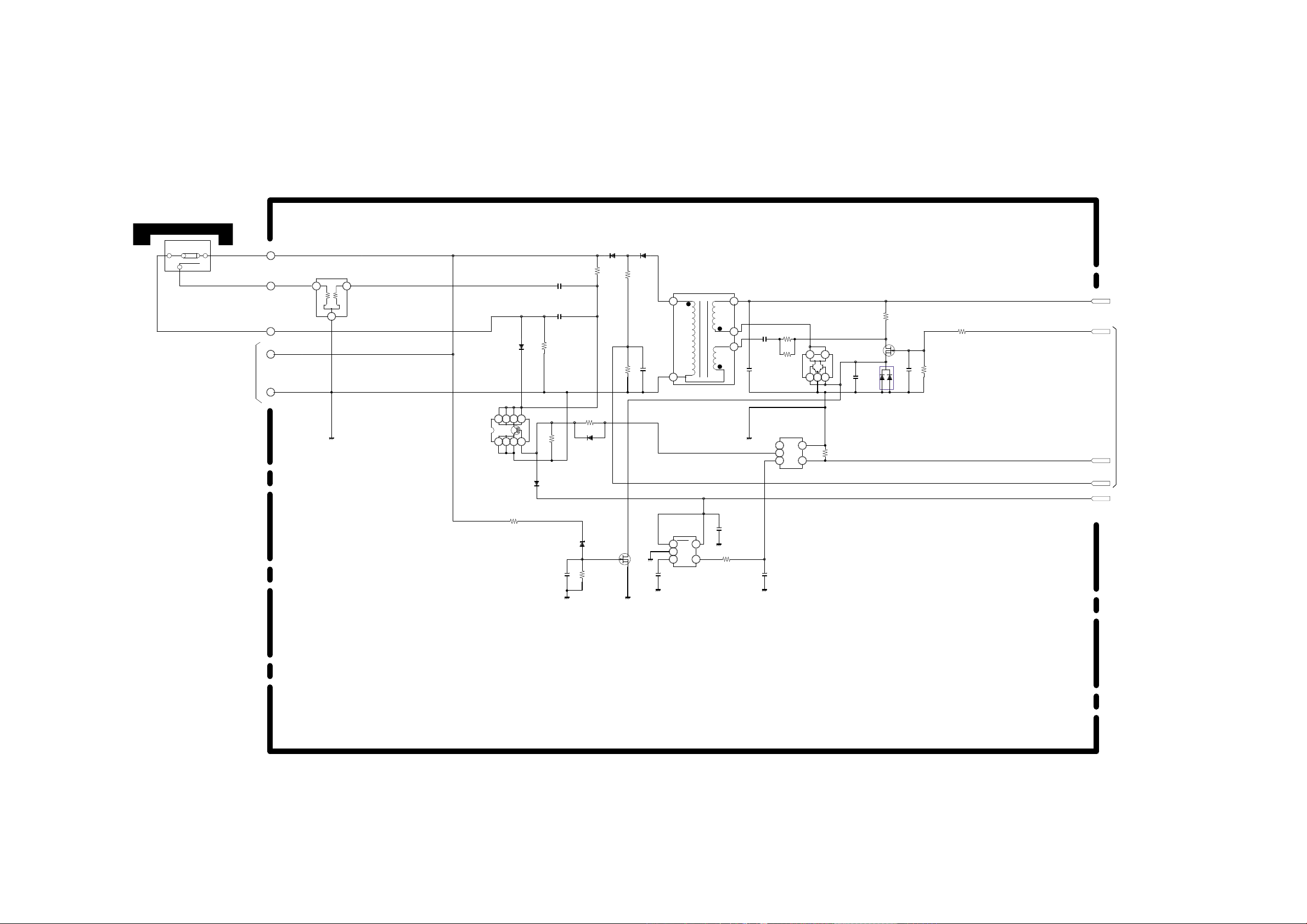
VAA31001-R.3651.A
- E14 ・ E5600 -
CP1(STA) 回路図
CP1(STA) CIRCUIT DIAGRAM
(K)
(K)
(K)
+12V(A)
XKT
STROBO UNIT
BLACK
BLUE
JW542
JW541
PINK
W1400
W1600
W1500
TRG
GRAY
XAN
OM/ORLIV006HZ
H=1.05
H=1.8
OM/ORDD72Z
OM/ORDD44ZOM/ORDD44Z
OM/ORZL17B0120GZ
H=4.8
OM/ORTR15Z
OM/ORSO08X1SANZ
OM/ORTR63Z
H=0.85
OUT
BP
IN
SHDN
GND
OUT
VDD
NC
IN
GND
OM/ORCC3316Z
3316
3216
3216
3216
3216
3216
2125
1608
FLASH REFLECTOR
LPK
3
CHG
UNREG(ST)
VMONIT
FLCTL
T5402
C5404
C5410
D5404
R5423
R5425
R5419
D5403
R5422
R5417
D5402
C5411
C5401
C5403
T5401
C5406
Q5407
Q5405
R5414
R5409
R5406
C5407
R5408
R5413
D5407
Q5409
C5415
Q5406
R5426
R5432
D5406
D5408
D5405
R5421C5408
C5416
C5414
Q5401
IC541
R5401
R5420
1AV4L17B0370N
1000P;B
0.033;350H
RR255LA-400
68;1/16J
100K;1/8J
91K;1/16D
RR264M-400
220K;1/8J
10M;1/8F
CRF02-Q
0.01;630H
22;6.3B
0.068;B
1AV4L17B0200G
0.01;B
3LN01S-E
CPH5504-E
1K;1/16J
1.2K;1/16J
100;1/16J
0.015;B
120;1/16J
10K;1/16J
DAN222
GT8G133
3LN01S-E
10K;1/16J
100K;1/8J
FC0300U
RB521S-30
RB521S-30
10K;1/16J0.1;B
1;B
0.1;B
0.1;B
TND721MH5
LK112M50
10K;1/16D
1K;1/16J
16V
1AV4L17B0200G
TXXGA0156433P
QLK112M50---P
UNREG(ST)
CHG
FLCTL
VMONIT
+12V(A)
2
1
8 7 6 5
13 2
4 5
2 1
543
1 432
5
43
2
1
5
43
2
1
REG.
TO ST1
JW551, 552
TO PWA
TO PWA
TO DMA(MAIN)
S2-68900/SX796-JNK
STA
Page 76
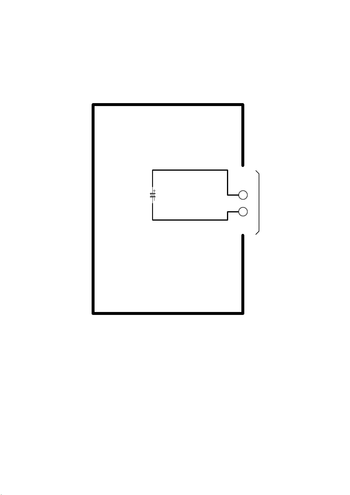
VAA31001-R.3651.A
- E15 ・ E5600 -
ST1 回路図
ST1 CIRCUIT DIAGRAM
JW551
BLACK
JW552
LPK
C5412
120u;300V
CEXAG579121AN
TO CP1(STA)
JM541, 542
S1-68900/SX796-JNK
ST1
Page 77
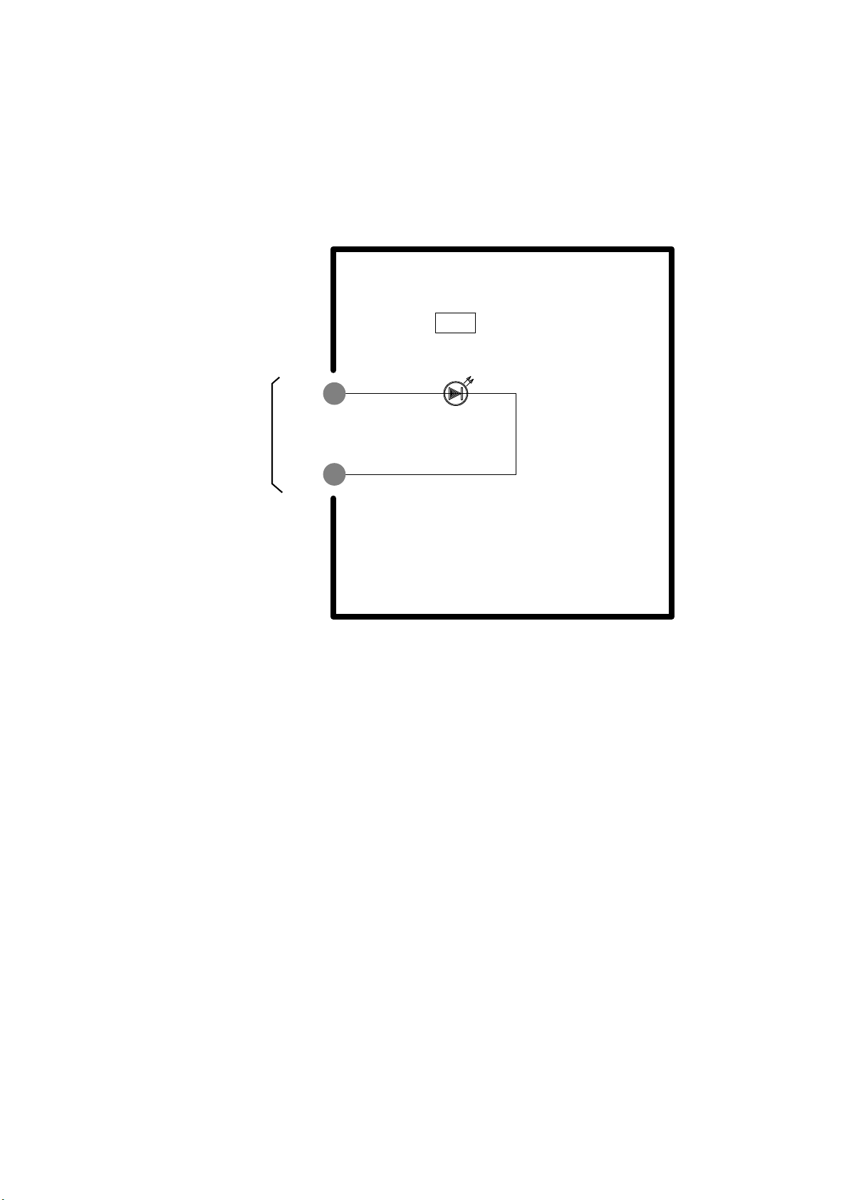
VAA31001-R.3651.A
- E16 ・ E5600 -
TB1 回路図
TB1 CIRCUIT DIAGRAM
NEW
OM/ORLE07AZ
H=0.8
CA
AN
JW601
JW602
TO CP1(SYA)
CL308, CL307
GRAY
WHITE
D6001
DLSML-511UW-G
SELF RED
T1-68900/SX796-JNK
TB1
Page 78
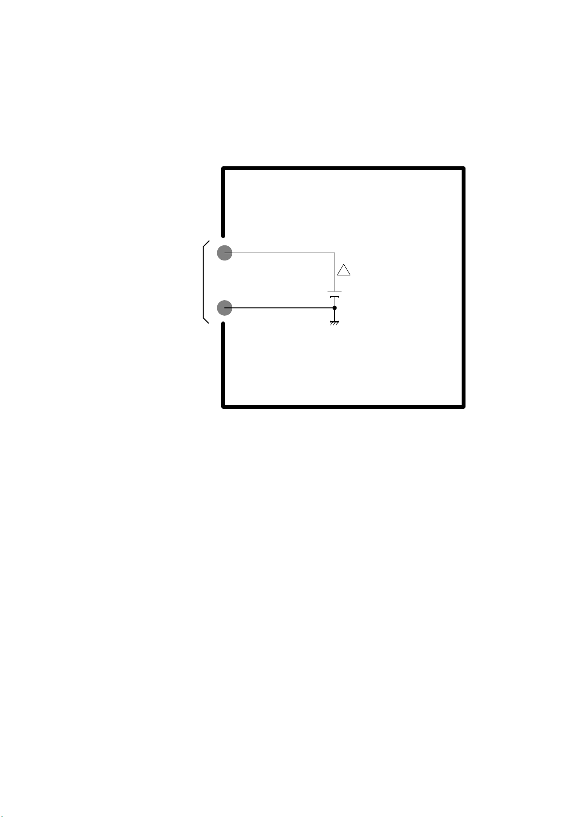
VAA31001-R.3651.A
- E17 ・ E5600 -
TB2 回路図
TB2 CIRCUIT DIAGRAM
TO CP1(SYA)
CN303
OM/ORZD20B07400HZ
H=2.5(1.85+BOND)
WT
BK
Z6501
ML614-TZ14
1AV4D20B09300
T2-68900/SX796-JNK
TB2
!
Page 79
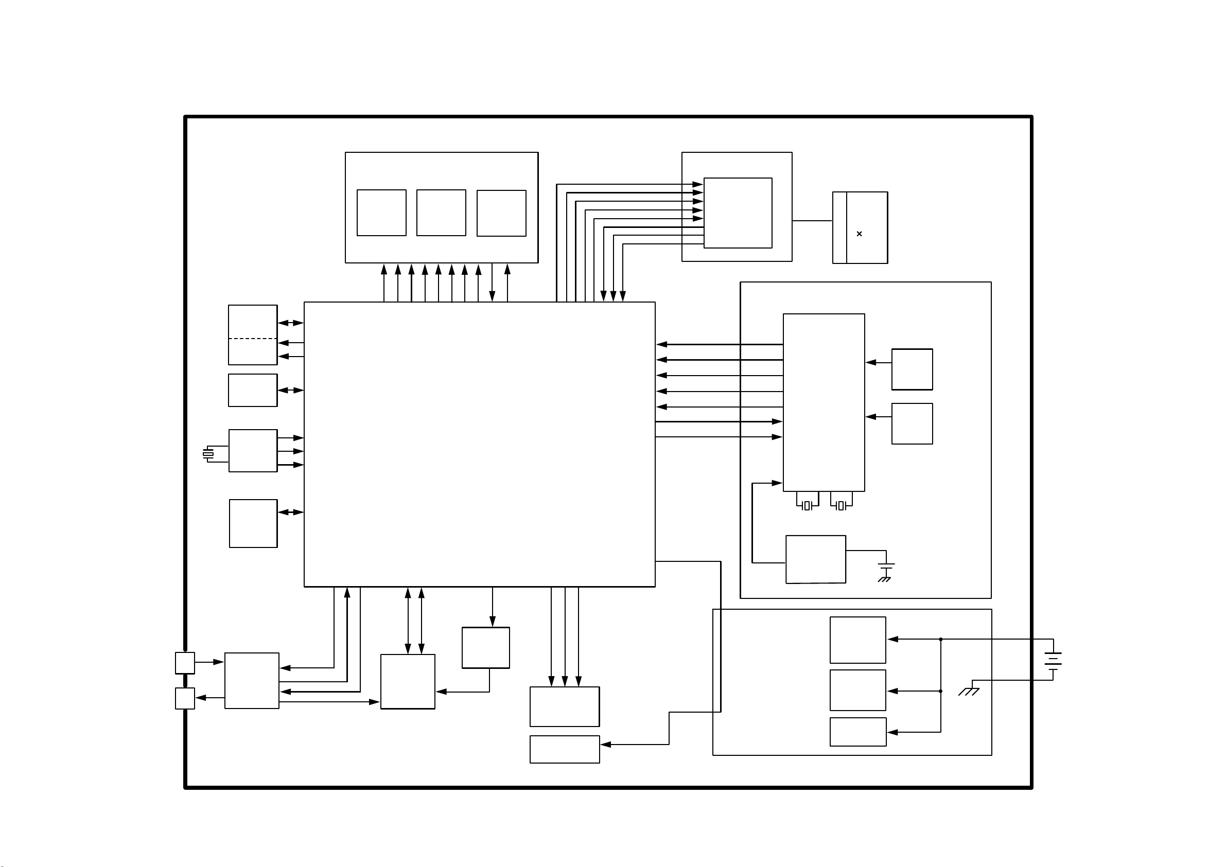
VAA31001-R.3651.A
- E18 ・ E5600 -
総合ブロック図
OVERALL BLOCK DIAGRAM
SDRAM
IC103
SD(0:31)
256Mbit
16Mbit
FLASH(NOR)
FLASH(NAND)
128Mbit
IC121
D(0:15)
FD(0:7)
A(1:20)
CKIN1
CKIN2
FSC4
IC111
CLOCK GENERATOR
28.63636MHz
X1101
CN143
SD CARD
IC181
AUDIO
DRIVER
FD(0:4)
LCD MONITOR
PADYOUT
LCDD (0:5)
LCDCLK
LCD TIMING PULSE X 5
IC152
VIDEO AMP
VOUT
CN110
USB/VIDEO
4MHz
X3001 X3002
32.768KHz
MRST
ZTEST
PLLEN
SCK
SDI
SDO
SREQ
CN301
IC301
8bit Micro Processor
LENS DRIVER
IC951
CN951
LENS
3
LENS BLOCK
Z6501
(TB2)
FSEN
FSMD 1:2
FSIN 1:2
PICTL
ZMIN 1:2
ZPULSE 1:2
ZRESET
FPI
XSUB
CCDCK
CCDSD
CCDEN
SUBGT
XV (1:6)
TGVD, TGHD
ADCK
AD (0:11)
XSG(1A,2A,1B,2B,3)
CCD BLOCK
IC101
ASI C
5M Pixel
IC903
V. Driver
IC901
IC905
CCD
CDS/AGC/AD-C
H. Driver
USBD+
PADAOUT
ASICAIN
AUDIO
CONTROL
SIGNALS X 5
USBD-
Ni-MH
CP1
LCD BACKLIGHT
LCD_AN
LCD_CA
DC/DC
CONVERTER
ELECTRONIC
FLASH
VDD
REGULATOR
IC302
LENS
DC/DC
CONVERTER
IC961
CN302
BACK SW UNIT
RELEASE UNIT
BL_ON
MIC
SPEAKER
AUDIO OUT
PWA BLOCK
SYA BLOCK
Page 80
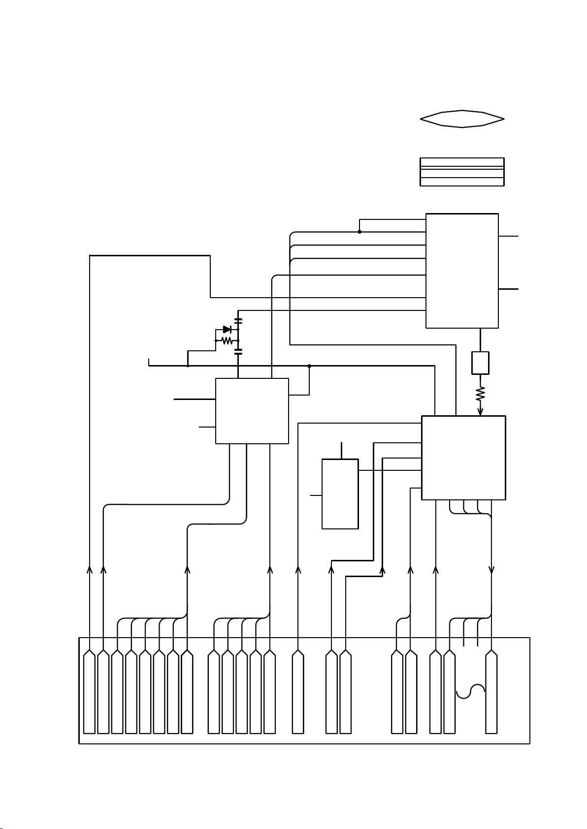
VAA31001-R.3651.A
- E19 ・ E5600 -
CCD ブロック図
CCD BLOCK DIAGRAM
LENS
CCD
EF
XV2
XV3
XV5
XSG1A
XV6
+12V(A) -6.0V(A)
MN39620
0D
PT
H1
RG
H2
VO
O_LPF
IC901
IC903
CH1, CH2, CH3, CH4, CH5
IV1, IV2, IV3, IV4, IV5, IV6
ISUB
Q9001
XV1
XSG2A
SUB
V. DRIVER
AN20101A
XSG1B
XSG3
SUB GT
IC905
CDS, A/D C
AD9948
D2:11
31
32
33
AD2
AD11
ADCK
CCDCK
CCDSD
CCDEN
VDC
IC904
REG.
TK11130CS
3.0V
4
1
+3.45V(A)
VDD3
TO DMA(MAIN)
IC101 ASIC
10
13
17
18
11
1:8
15
19
1, 2, 21, 23, 24
20, 25, 22, 26, 28, 27
3
25
9
2-4. 7-13
27
18, 19, 14, 15, 21
8
+12V(A)
+3.45V(A)
-6.0V(A)
6,184, 5
26, 24, 37, 6
TGVD
TGHD
34, 35
17, 22
H. DRIVER
14
SUBSW
16
HL
XV4
XSUB
XSG2B
V1,V2,V3A,V3B,V4,V5A,V5B,V6
9-16
Page 81
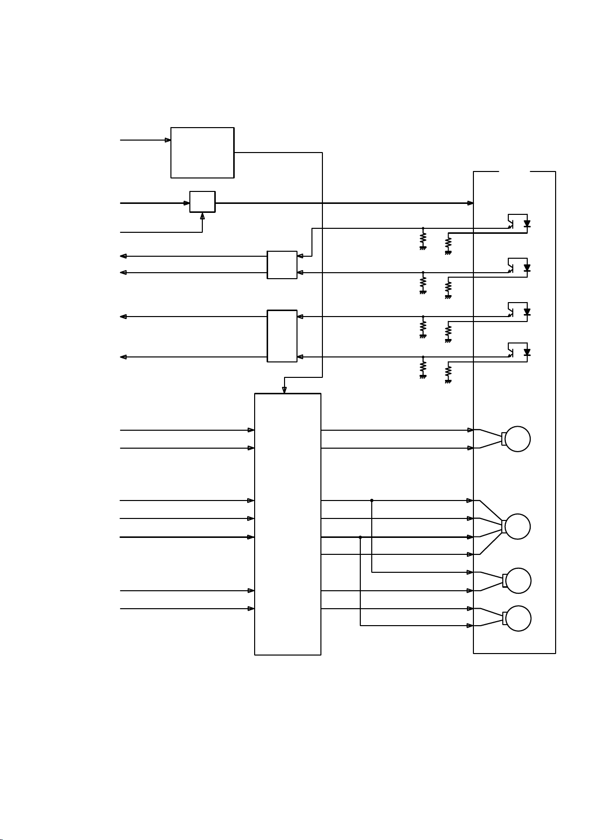
VAA31001-R.3651.A
- E20 ・ E5600 -
LENS ブロック図
LENS BLOCK DIAGRAM
FOCUS/
IR/SH DRIVER
OUT1
OUT4
UNREG
ZM.M
OUTB
OUTA
DC 1-
DC 2+
INB
INA
ZOOM DRIVER
LB8655T
IC951
EN
MD1
MD2
2B
1B
2A
1A
OUT2
OUT3
OUT5
OUT6
FC.M
SH.M
IR.M
ZPLUSE1
ZPLUSE2
PICTRL
(IC101 198pin)
VDD3
FOCUS_PI
CN951
UNIT LENS
ZPULSE1
(IC101 213pin)
ZMIN1
(IC101 209pin)
ZMIN2
(IC101 208pin)
FSEN
(IC101 203pin)
FSMDI
(IC101 202pin)
FSMD2
(IC101 201pin)
FSIN1
(IC101 200pin)
FSIN2
(IC101 199pin)
FPI
(IC101 206pin)
SHUTTER+
SHUTTER-
IRIS+
IRIS-
19
18
6
7
20
17
8
9
11
10
3
5
13
ZOOM_PI
16
Q9509
IC961
L9601, D9601
Q9601, C9603
SW REG.
BOOST4.25V
ZRESET
(IC101 210pin)
Q9501
Q9502
ZPULSE2
(IC101 212pin)
PIV
1, 14
2
4
15
12
3
4
8
9
5
6
7
IN1
IN2
16
15
21
20
18
17
22
19
Page 82
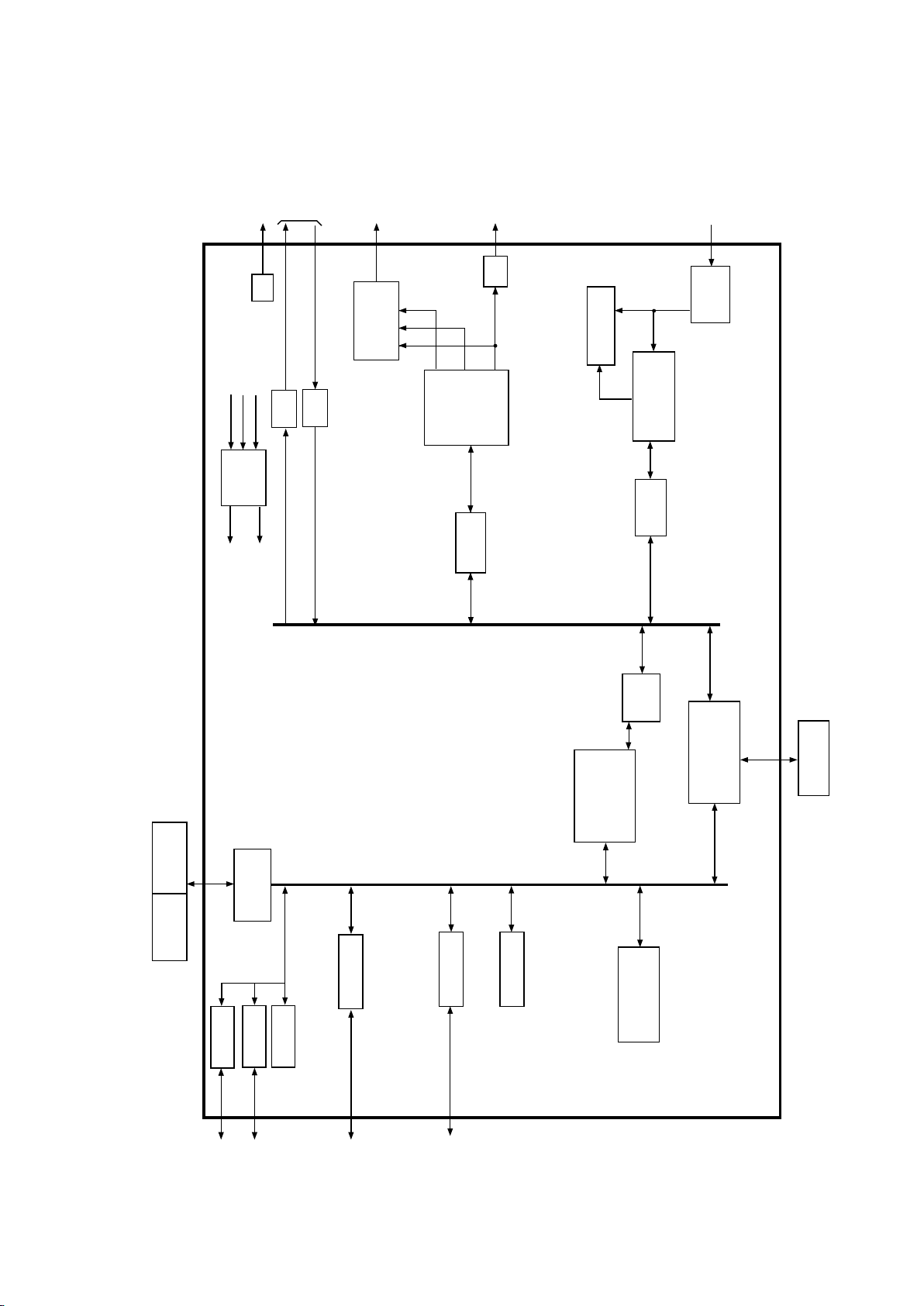
VAA31001-R.3651.A
- E21 ・ E5600 -
ASIC ブロック図
ASIC BLOCK DIAGRAM
DIGITAL
CLAMP
SIGNAL
PROCESSOR
AF,AE,AWB
SRAM
SRAM
D/A
COMPOSITE
VIDEO
NTSC/PAL
ENCODER
SRAM
BUS
BUS
DIGITAL
I/F
A/D
D/A
TG
CLKGEN
PLL
SDRAM
CONTROLLER
JPEG
CONTROLLER
CCD
98MHz
4fsc
36MHz
72MHz
ARM
UART
USB
SD
PWM
SIO
IC301
MICRO
PROCESSOR
EXT PORT
(LENS DRIVER)
PIO
BUS I/F
FLASH
(NOR)
SDRAM
CCD
BLOCK
IC101 ASIC
RGB
6bit DATA
CCD
DRIVER
AUDIO
DRIVER
SD CARD
USB
CONNECTOR
FLASH
(NAND)
Page 83
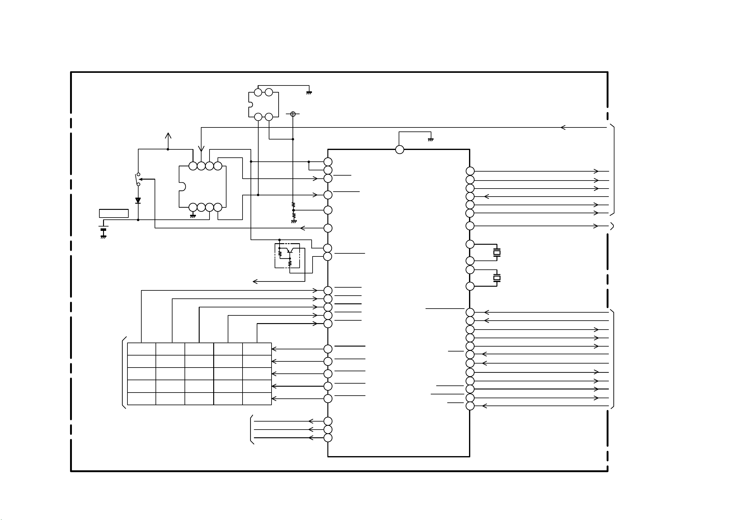
VAA31001-R.3651.A
- E22 ・ E5600 -
SYSTEM CONTROL ブロック図
SYSTEM CONTROL BLOCK DIAGRAM
33
34
35
28
4
3
29
9
7
6
10
38
20
42
30
46
27
39
37
26
2
17
12
24
5
6
7
8
1
2
3
4
16
13
14
43
15
31
23
8
32
18
45
X3001
X3002
32KHZ
4MHZ
41
XIN
XOUT
XCOUT
XCIN
VMONIT
CHG ON
PLLEN
BEEP
LCD ON2
PA ON
P ON
VSS
LCD ON
SELF LED
VMONIT
CHG
BOOST4.25V
SREQ
P ON
PA ON
SPORTS
NIGHT
VIEW
OK
SCENE
LANDSCAPE
PORTRAIT
SET UP
PW_ON
LCD ON
1st
SI
21
LI
IC302
BATTERY
BACKUP
BAT
OFF
AL3.2V
UNREG
VDD
RESET
ALWAYS3.2V
IC304
RESET IC
4
3
1
2
OUT
VDD
VSS
BACK UP
SO
AUTO
2nd
MOVIE
SW3.2V
Q3001
TELE
MENU
DEL
WIDE
--
PW_TEST
PLAY
RIGHT
LEFT
UP
DOWN
CN302
CN301
CN301
CN302
TEST
AVJACK
BACKUP CTL
SCAN OUT0
SB_LED (R)
AF_LED (G)
IC301
8bit MICRO
PROCESSOR
SCAN IN0
SCAN IN1
SCAN IN2
SCAN OUT1
SCAN OUT2
PW_LED
RESET
BAT OFF
BATTERY
SCAN IN3
SCAN IN4
AV REF ON
AVREF
SCAN OUT3
VDD
VDD
SCAN OUT4
SCK
36
ASIC TEST
1
22
MAIN RESET
CARD
47
25
COMREQ/BOT
USB_CONNECT
TO DMA(MAIN)
TO DMA(MAIN)
TO TB1
PLLEN
BEEP
LCDON2
SREQ
SDO
SDI
SCK
ZTEST
MRST
ZCARD
COMREQ
USBCNT
Z6501
(TB2)
Q3002
BOOST4.25V
44
SELF LED
PA ON2
48
PA ON2
UNREG
5
Page 84
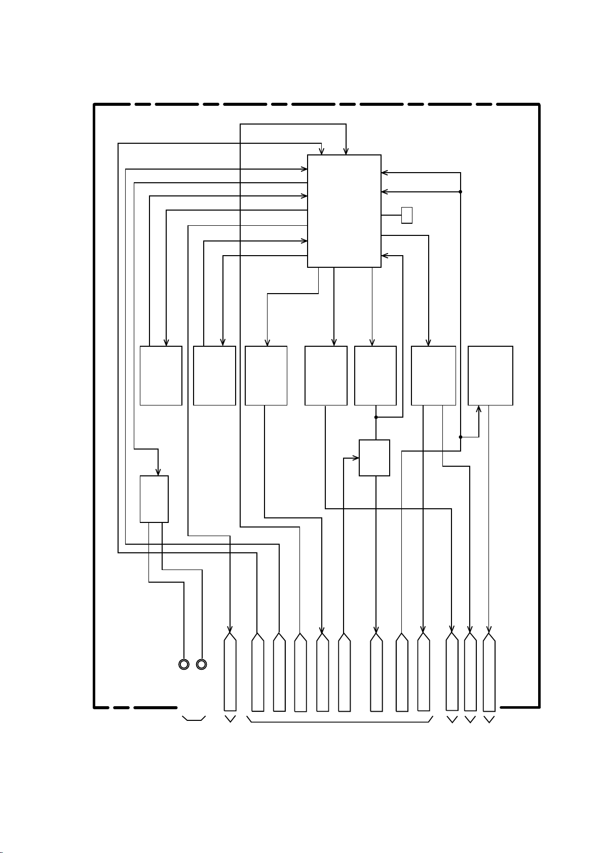
VAA31001-R.3651.A
- E23 ・ E5600 -
POWER ブロック図
POWER BLOCK DIAGRAM
IC501
SWITCHING
CONTROL
BD9739KN
T5001,Q5001
CONVERTOR
TRANS
IC961
STEP UP
CIRCUIT
Q9601, L9601
L5003, Q5003
STEP UP
CIRCUIT
L5005
STEP DOWN
CIRCUIT
L5006
STEP DOWN
CIRCUIT
+12V(A)
-6.0V(A)
+3.45V(A)
4.25V(PON_H), 3.7V(PON_L)
BOOST4.25V
OUT4
OUT1M
DRAIN2L
DRAIN2H
DRAIN3L
L5004, Q5004
STEP UP
CIRCUIT
OUT6
L5007
STEP UP
CIRCUIT
CURRENT
DETECTOR
CIRCUIT
IC502
REG.
OUT7B
LCD_AN
LCD_CA
58
62
6319
20
17
53
6, 7
4, 5
10, 11
16
15
51
55
34
VR
VR501
+12V(L)
PA ON2
LCDON
BLON
PON
TO DMA(MAIN)
TO DMA(LCD)
TO DMA(MAIN) & STA
TO DMA(MAIN, LENS)
TO DMA
(MAIN, LCD, LENS)
TO LCD
BACK LIGHT
SWIN6
SWIN7
SWOUT6
SWOUT7
STB6
STB23
STB1
STB7
STB4
2
3
VDD3
VDD1.41
PAON
Page 85
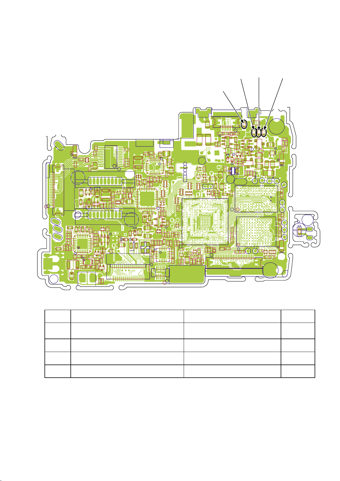
VAA31001-R.3651.A
- E24 ・ E5600 -
FUSE arrangement (CP1 PCB)
FUSE Function of FUSE Phenomenon when FUSE has blown out Rating
F5001
Protection of the DC/DC converter and
the system computer circuit
The power is not turned on. 2A 32V
F5002 Protection of the DC/DC converter The power is not turned on. 2A 32V
F5004 Protection of the lens circuit The power is not turned on. 2A 32V
F5005 Protection of the speed light circuit The speed light is not charged. 2A 32V
1
2
32
CN171
IC181
IC181
1
7
8
14
15
21
22
IC903
CN951
CN951
1
20
CN191
IC951
IC951
1
9
10
18
1
8
9
14
15
22
23
28
IC901
C9017
1
10
11
20
21
30
31
40
IC905
1
3
4
6
IC152
IC182
C1513
X1101
IC111
1
5
6
10
11
15
16 20
1
5
6
10
CN304
1
24
CN302
CN302
IC101
1
3
4
5
IC904
IC121
IC103
CN193
CN192
CN301
CN301
1
6
13
4 5
IC541
VR501
C9035
VDD3
GND
TDI
TDO
TMS
SCNEN
JSEL
TCK
TRST
ZFRD
ZFWR
VDD1.41
LCD_AN
RD
LCD_CA
WT
SP-
WT
SP+
RD
MIC
RD
GND
BK
BAT+
JW501
BAT-
JW502
CN171
SX796_CP1
SIDE-B
2A
F5002
2A
F5001
F5005
2A
2A
F5004
33
1
3
4
5
9
XF901
D1701
D5408
D5405
C9008
1AG4B10F1600AB
+
+
1
10
12
13
20
24
+
+
+
IC901
C1512
D1702
D1703
IC182
DISCHARGE
MIC
CL301
CL302
CL303
BOOT
28
GY
WT
SIDE-B
1600BB
SX796
TB1
C1707
C1701
R5016
R501
5
R5013
R5012
C5411
R5425
R5004
VR501
VA305VA303VA304
C5028
F5004
F5005
F5002
Q5003
F5001
C5033
L5002
R5026
C5031
R5024
R5023
C503
0
R5022
Q5001
L5010
L5009
L5001
C5032
C5029
R5414
R5413
C5406
Q5407
D5407
C5407
Q5405
C5414
C5416
R5420
C5415
IC541
R5401
Q5401
R5423
D5007
C1905
R1902
C1904
C1004
C1003
C1018
C1002
R1002
RB10
4
C1519
R1103 C1101
Q1736
CB181
IC182
C1815
C1830
C1823
C1824
C1803
R1812
C1831
C1829
C1828
R1815
C1810
R1814
C1825
R1813
R1806
C1827
C1806C1807
Q1735
R1735
R1736
R1811
R1801
C1820
C1821
C1822
IC181
C1512
C1505 C1515
R1503
R1509
C1504
R1502
Q1505
IC152
R1501
L1101
C1114
R1102
L1103
L1102
C1105 C1102
R1111
C1103
C1104
R1104
X1101
D9001
R9508
C9032
R9007
R9013
C9026
C9014
C901
6
C9015
C9018
R9008
C9024
D9003
D9004
C9017
C9505
C9502
C9504
CB951
R9501
C9503
IC951
R9505
C9506
C9501
R9014C9027
R9010
XF901
L9002
R9006
R900
5
C900
3
CB904
C9034
C9036
C9035
C9030
C900
6
CB902
CB903
C9023
R9002
CB901
IC904
C9005
L9001
C9007
C9008
C9012
C9013
RB90
1
C9009
RB903
R9015
R901
6R9003
C9025
IC905
IC901
R1431
Q1431
Q1432
RB142
R143
4
R1410
RB143
R1404
RB144
R120
1
C1201
L1080
C1085
C108
3
R100
3
C1058
Q1051
R1066
R1057
C1051
R1052
R1053
R1055
C1052
C1001
R1064
C1057
C1050
IC101
R1018
RB108
RB106
RB10
1
RB10
3
RB105
RB10
2
R1001
C1903
C1901
C1020
C1007
L1001
C1086
C1084
C1009
R1047
R1046
C1019
R1005
C1005
C100
6
C1059
R1093
R1054
RB107
C1056
C1054
VA307 VA30
6
C1706
C1705
R1701
R1702
C1513
CN304
C1708
C1734
D1701
D1702
D1703
C1702
C1826
CN171
CN191
CN192
CN193
CN302
CN301
Q9001
L9003
L9004
RB90
4
RB902
R9019
R9018
R9020
R900
1
L9005
C9011
C9010
R9004
C9028
IC103
IC121
R9510
IC111
CN951
VA309
C1703
D5408D5405
C5037
C1709
D6001
F5001
F5002
F5004
F5005
Page 86

VAA31001-R.3651.A
- E5600 -
The contents of inspection standards and tools for
E5600
[1] Inspection standards ............................................................................................................................................ R1 to R10
[2] Tools .................................................................................................................................................................... T1 to T5
Page 87

INSPECTION STANDARDS
Item Criteria Applied tool(s)
External view
VAA31001-R.3651.A
Gap/Difference in
height
Outside and inside
status
Operation/Operability
Operation
・ General components
Gap: 0.3mm or less
Difference in height: 0.15mm or less
・ When the battery case is opened/closed:
Gap in its periphery: 0.3mm or less
Gap in the bottom: 0.5mm or less
Difference between right and left: 0.2mm or less
Stepped difference: 0.5mm or less
・ There must be no noticeable damage, stain, sink mark, welded
mark, unevenness, crack or oil exudation.
・ When pushing the main body, noticeable noise must not be heard.
(Observe and check it by naked eyes under fluorescent lamp and
natural sunshine.)
・ While operating, any irregularities or irregular noise shall not be
required.
Visual observation
Primary battery/
Secondary battery
Operability of buttons
Mode dial
Operation touch
Each cover
(Check it by shaking the camera while operating. Lightly hit the
camera onto the Linoleum-laid desk while operating.)
・ No cave-ins of the buttons shall be required.
・ Operator must feel "click" on each button.
・ "Click" must occur when or after a switch is ON.
(Check it while operating normally.)
・ When clicking, normal touch shall be required. Any outstanding
"caught-in-mechanism" touch or "rubbed-in-mechanism" touch or
play shall not be required.
(Check and observe the condition through normal operation.)
・ When operating a lever or knob by hand, any irregular conditions
shall not be required.
(Operate the camera in the actual photography procedure and check
the operation touch.)
・ When closed, there must not be an extreme play.
・ Each cover can be opened/closed without any outstanding
"caught-in-mechanism" touch or "rubbed-in-mechanism" touch or
abnormal noise.
(Open and close each cover and check it.)
- R1・ E5600 -
Page 88
Monitor
VAA31001-R.3651.A
Item Criteria Applied tool(s)
Shooting image ・ Inclined degree of image shall be 0.5 degree or less.
・ PC monitor and print output
(Output will be evaluated while the display range boundary of LCD
unit is regarded as standard when the through-the-monitor image is
made.)
Lens capacity
Focal length
Open aperture F No.
Wide-end position (Compelling ∞ )
5.7 mm + 7.1%
- 1.1%
Tele-end position (Compelling ∞ )
17.1 mm + 0.9%
- 6.9%
Wide-end position (Compelling ∞ )
F2.9 + 5.8%
- 2.3%
Tele-end position (Compelling ∞ )
F4.9 + 10.6%
Photoshop
Printer
Focal length
measuring instrument
Lens drive tool
Peripheral light reduc-
tion
Ghost/Flare
Point light source
Surface light source
Distortion
Dust in a picture
+ 2.1%
・ Against the picture center, the luminance of the nearest peripheral
area must be 35% or more.
・ Against the picture center, the luminance at 70% of the image
height must be 55% or more.
・ There must not be an outstanding ghost/flare.
・ There must not be an outstanding flare at the center.
・ There must not be an outstanding deformation.
・ There must not be an outstanding dust in a picture.
・When the picture center (within the circle whose diameter is 80%
of the short side) is Zone I and its outside is Zone II, the light
reduction against the periphery must be as follows :
a b
Zone I 4 or less 0
Zone II 10 or less 2 or less
a : 1.5% or less
Visual observation
Photoshop
CRT monitor
PC
b : More than 1.5% and less than 3.0%
- R2・ E5600 -
Page 89

Lens barrel
VAA31001-R.3651.A
Item Criteria Applied tool(s)
Zoom / Focus ・ There must not be an abnormal action (for example, the unit oper-
ates one-sidedly or its operation is not smooth or it is caught).
(As changing the camera's posture, check it in all the directions.)
AF
Distance measurement
operation
Shortest photograph
distance
Normal
Macro
Shooting with a speed
light
Light adjustment accu-
・ In the case of normal AF: Focus must be fit at the picture center.
・ In the case of the out-of-focus object: Focus must be fit at the 2m
point.
・ In the case of the scene mode: Focus must be fit in the selected
area.
Focus must be fit at the following distance.
・ 30cm (in whole area)
・ 12cm(Z00) 、7.8cm(Z14) 、4 cm(Z04 ) 、10 .5 cm(Z1 9)、
4.7cm(Z09)
・ Tele-end: 0.4 ~ 2.0m
Visual observation
Visual observation
Tape measure
EIAJ chart
Siemens chart
Standard reection
racy
Guide No. FULL
(ISO100・m)
Recycling time
Wrong flash
・ Wide-end: 0.4 ~ 3.3m
・ Macro-wide-end 0.4 ~ 3.4 m
In the above range, ± 0.5 Ev or less
(Photography mode: AUTO , ・ Speed light: Compelling flash)
・ 6.8 ± 0.4 EV
(Charge for 10 seconds with the new primarybattery and perform
measurement within 1 second.)
・ Within 8 seconds
・ Perform charging with a new primary battery for 10 seconds and
carry out full flashing within 1 second. Then, measure the time
taken until the speed light LED finishes blinking while pressing
lightly the shutter release button (including the ON/OFF time of
the monitor LCD).
・ Wrong flash must not occur.
(Check by loading/unloading a battery, giving a light shock and
operating mode buttons except S2.)
plate
Flash meter
New battery
Measurement
rmware
Stop watch
New battery
- R3・ E5600 -
Page 90

Item Criteria Applied tool(s)
Quality of image
VAA31001-R.3651.A
Resolution in AF The resolution must be in compliance with the following values in
all the postures of the EIA J chart evaluation.
<High quality of image>
Center horizontal/vertical: 1150 TV pcs.
Periphery horizontal/vertical: 750 TV pcs.
<Standard>
Center horizontal/vertical: 1150 TV pcs.
Periphery horizontal/vertical: 750 TV pcs.
<3M>
Center horizontal/vertical: 900 TV pcs.
Periphery horizontal/vertical: 600 TV pcs.
<Personal computer>
Center horizontal/vertical: 450 TV pcs.
Periphery horizontal/vertical: 300 TV pcs.
<TV>
Center horizontal/vertical: 250 TV pcs.
Periphery horizontal/vertical: 150 TV pcs.
EIAJ chart
Photoshop
Siemens chart
<10 ~ 0.3m> (The whole zoom area)
Center horizontal/vertical: 1150 TV pcs.
<0.3 ~ 0.04m> (The whole zoom area)
Center horizontal/vertical: 950 TV pcs.
・ Take a picture on condition that aperture is "open" in the AUTO
mode and image quality priority mode.
・ Equip the 5100K viewer with the chart with WIDE-end, MIDDLE
(Z08), TELE-end and the distance of 0.3m or more and shoot an
object in the full range of angle of view.
・ Then, open the recorded image data file through Photoshop and
check the resolution visually.
・ Check each posture and the difference of zoom reciprocation.
・ Take a picture in each quality mode.
・ Measure the TV resolution pieces at center.
In the case of “Macro” <Macro>
Center horizontal/vertical: 950 TV pcs.
・ Check at near distance (W12cm, M (Z08) 4cm, T10.5cm).
・ Take a picture at the high image quality mode.
- R4・ E5600 -
Page 91

Item Criteria Applied tool(s)
In the case of compel-
<Compelling infinity> (The whole zoom area)
VAA31001-R.3651.A
Infinity chart
ling infinity
In the case of “our of
focus”
Gradation/luminance
level
Center horizontal/vertical: 950 TV pcs.
・ Shoot the infinity collimator image on condition that aperture is
"open" in the scene distance view/night view mode and the image
quality priority mode.
・ Then, open the recorded image data file through Photoshop and
check the resolution visually.
<Out of focus> (The whole zoom area)
Center horizontal/vertical: 950 TV pcs.
・ Measure the TV resolution pieces at center.
・ Check each posture and the difference of zoom reciprocation.
・ Put a chart at the distance of 2m, set it in the "out of focus"
condition and shoot it. (Use a white paper to set it in the "out of
focus" condition.)
[Histogram's gray average value]
・ Black: 12 ± 5
EIAJ chart
Photoshop
Siemens chart
5100K viewer
ITE γ 0.45
Gray: 130 ± 15
White: 225 ± 10
・ Equip the 5100K viewer with a scale and shoot an object in the
full range of angle of view while the AUTO mode and the image
quality priority mode are set.
Open the recorded image data file through Photoshop and pick up
a measurement section with the each color (its central area 64 ×
64 pixels) with the rectangle selector tool.
・ Read the histogram's gray value and the gray standard deviation.
・ Measurement section
Luminance level:
Upper left 1 step: Black, 6 steps: Gray, Center: White
Lower left 6 steps: Gray, 11 steps: Black
Gray scale (standard)
Photoshop
- R5・ E5600 -
Page 92
Item Criteria Applied tool(s)
Quality of image
VAA31001-R.3651.A
Noise [Histogram's standard deviation]
・ Gray: 3.0 or less
Black: 3.0 or less
・ Equip the 5100K viewer with a scale and shoot an object in the
full range of angle of view while the AUTO mode and the image
quality priority mode are set.
Open the recorded image data file through Photoshop and pick up
a measurement section with the each color (its central area 64 ×
64 pixels) with the rectangle selector tool.
・ Read the histogram's gray standard deviation.
・ Measurement section
Noise:
Upper left 2 step: Black, 6 steps: Gray
Lower left 6 steps: Gray, 10 steps: Black
Reproduction of color ・ Color
R G B
W 209 ± 20 209 ± 20 209 ± 20
Ye 209 ± 20 209 ± 20 47 ± 15
R 215 ± 20 15 ± 10 10 ± 10
5100K viewer
ITE γ 0.45
Gray scale (standard)
Photoshop
Color bar chart
Photoshop
・ Equip the 5100K viewer with a chart and shoot an object in the
full range of angle of view in the AUTO mode and the image
quality priority mode (high image quality mode).
・ Open the recorded image data file through Photoshop and pick up
a measurement section with each color (its central area 64 × 64
pixels) with the rectangle selector tool.
・ Read the histogram's RGB.
- R6・ E5600 -
Page 93
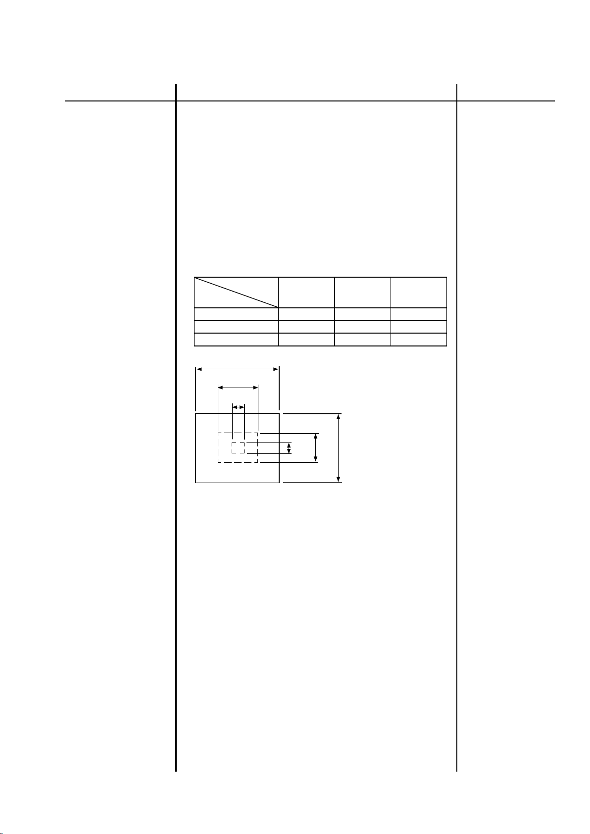
Finder
VAA31001-R.3651.A
Item Criteria Applied tool(s)
View / Image
Visual field frame/
frame line
Shading
Operation
Dust, fluff and damage
・ There must be no blur, distortion, ghost, halation or other out-
standing troubles in contrast, gradation, etc.
・ Blur or difference in thickness must be within the proper range to
operate the stamped line and visual field frame.
・ You can check the whole finder visual field.
・ The finder must be activated smoothly in a link operation with the
lens barrel zooming action.
・ The position and quantity must be as follows
Zone
A B C
Size
Less than 10 μ m 0 pc 2pcs or less 3pcs or less
10 ~ 20 μ m 0 pc 0 pc 1pcs or less
More than 20 μ m 0 pc 0 pc 0 pcs
b
b/2
b/6
・Total:3pcs or less
・Interval:Less than b/2
Visual observation
Visual observation
Visual observation
A
B
C
a/8
a
a/2
- R7・ E5600 -
Page 94
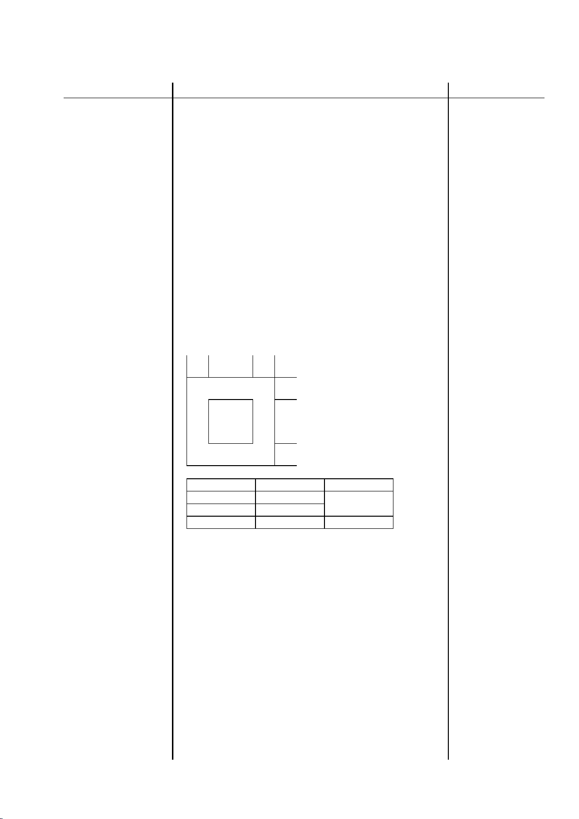
Item Criteria Applied tool(s)
LCD and others
VAA31001-R.3651.A
Monitor LCD View
Visual eld ratio
Bright pixels or dim
pixels on LCD
・ The reproduction of W, B and RGB must not be interfered.
・ The monitor LCD must comply with the SY monitor LCD perfor-
mance standard.
・ There must be no shading in the LCD display range.
・ The inclination of the image and the monitor frame must be ±
0.75° or less.
・ The vertical difference and horizontal difference of the black belt
width in the image periphery must be within 0.3mm.
・ Through-the-monitor image: 96 to 100%
・ Play-back image: 98 to 100%
・ Perform reproduction for each single color of R, G, B and white
and check visually.
1 2 1
1
Visual observation
Visual observation
Visual observation
Self-timer
Operation time:
LED blinks/lights
Zone A 2
Zone B 1
Zone Bright pixel Dim pixel
A 1
B 3
Total 4 6
・ Bright pixels: Visible normally through 5% ND filter
・ Dim pixels: Visible normally (Standard: Within the above
quantity)
・ 10 ± 1 second
・ Blinks 9 times and lights for 1 second.
(Measure the time until release is done since the shutter release
button was lightly pressed.)
6
Visual observation
Stop watch
- R8・ E5600 -
Page 95

Item Criteria Applied tool(s)
Electric characteristics
VAA31001-R.3651.A
Constant voltage
Consumption current
Stand-by
Start (Photography)
B. C voltage
When voltage
decreases
(Alkaline battery)
Level 1
Level 2
Level 3
(Ni-MH)
Level 1
Level 2
・ When card is not used: 0.27mA or less (when the power switch
is OFF)
・ When card is used: 0.39mA or less (when the power switch is
OFF)
・ 12mA or less (at "Sleep")
・ 0.75W or less (when the power switch is OFF
・ 2.125 ± 0.1V
・ 2.0 ± 0.1V(The battery mark blinks.)
・ There is no regulation of voltage. (Power OFF)
・ 2.35 ± 0.1V
・ 2.0 ± 0.1V (The battery mark blinks.)
power supply
Ammeter
Dummy battery pack
Constant voltage
power supply
Volt meter
Dummy battery pack
(Li battery)
Level 3
Level 1
Level 2
Level 3
・ There is no regulation of voltage. (Power OFF)
・ 2.425 ± 0.1V
・ 2.0 ± 0.1V (The battery mark blinks.)
・ There is no regulation of voltage. (Power OFF)
・ Connect the constant-voltage power supply to the dummy battery
pack and decrease the power supply voltage 1 second before.
The voltage is under the following conditions now. Measure the
voltage (excluding "When voltage increases").
・ Level 1 : The battery "half" mark lights on the monitor LCD.
・ Level 2 : The "no battery capacity" warning appears on the
monitor LCD.
・ Level 3 : Power OFF
・ In the case of the voltage at Level 1, also measure the voltage
when pressing lightly the shutter release button.
・ When measuring the voltage at Level 3, the power must be
automatically turned off after 30 seconds since the voltage
reached Level 2. The voltage must not be regulated.
- R9・ E5600 -
Page 96

Item Criteria Applied tool(s)
Electric characteristics
When voltage
increases
(Alkaline battery)
VAA31001-R.3651.A
(Ni-MH)
(Li battery)
Level 1
Level 2
Level 1
Level 2
Level 1
Level 2
・ 2.25 ± 0.1V
・ 2.1 ± 0.1V
・ 2.45 ± 0.1V
・ 2.1 ± 0.1V
・ 2.6 ± 0.1V
・ 2.1 ± 0.1V
・ Connect the constant-voltage power supply to the dummy battery
pack and check the voltage at Level 3 ("no battery capacity"
indication). Then, turn off the power, increase the voltage by
0.1V and change the power switch from OFF to ON. The voltage
is under the following conditions now. Measure the voltage.
(When changing the voltage, turn off the power.)
・Level 1 : The battery mark is turned off on the monitor LCD.
・Level 2 : The battery "half" mark lights on the monitor LCD.
- R10 ・ E5600 -
Page 97
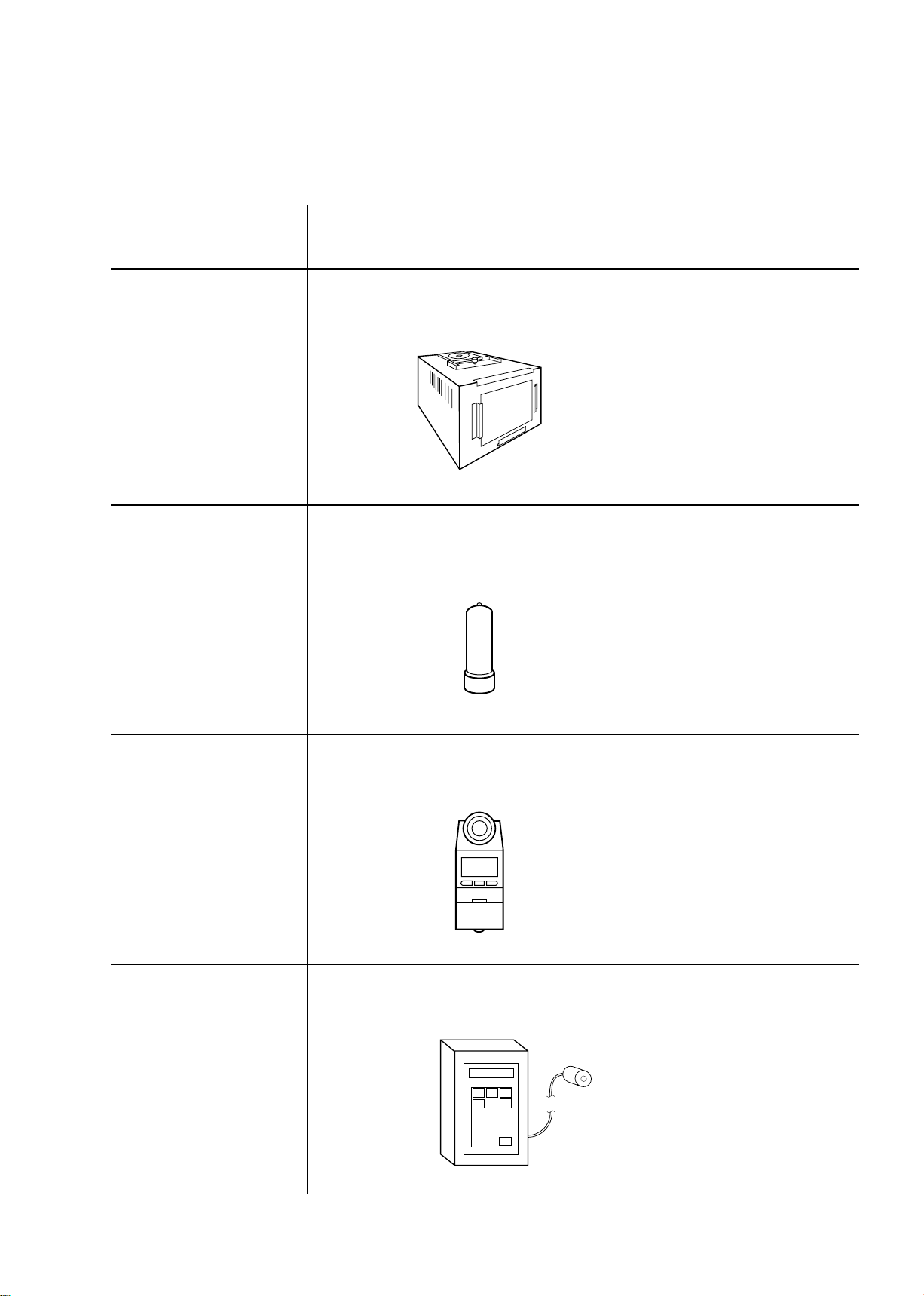
[2] 工具一覧表 Tool List
POWER
BM-3000
VAA31001-R.3651.A
※:新規工具
※:New tool
工具番号
Tool No.
名 称
Name
J63080 パターンボックス LV-1450DC
Pattern Box LV-1450DC
J63080A 交換用ハロゲンランプ (LV-1450DC 用 )
Spare Harogen Lamp (For LV-1450DC)
備 考
Remarks
共通 (E4300, E3500,
E3100, E2100, E5400,
E3700, E3200, E2200,
E8700, E4100, E4600,
E5600)
Common(E4300, E3500,
E3100, E2100, E5400,
E3700, E3200, E2200,
E8700, E4100, E4600,
E5600)
LV-1450DC
Exclusive
J63081 カラーメータ ( ミノルタカラーメータⅢ F)
Color Meter(Minolta Color meter Ⅲ F)
J63068 輝度計 BM-3000
Luminance Meter BM-3000
共通
Common
共通
Common
- T1・ E5600 -
Page 98
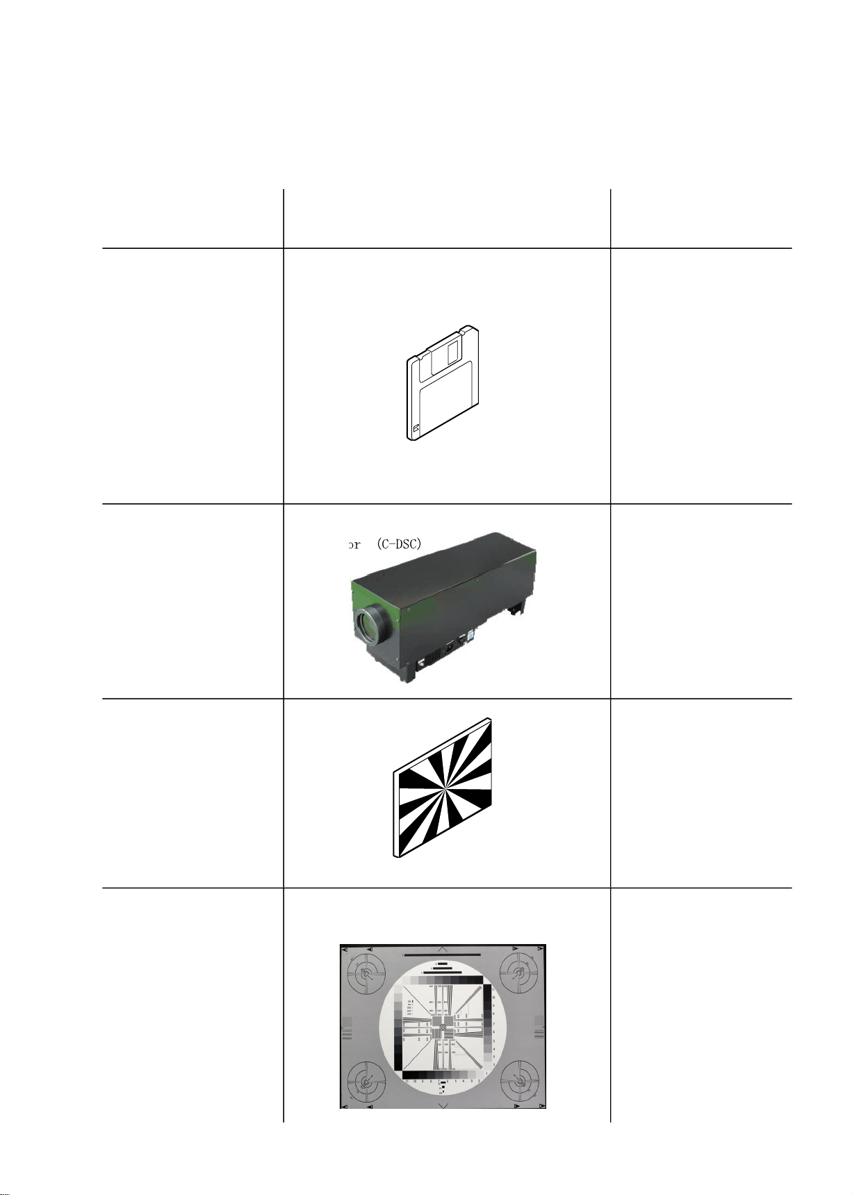
VAA31001-R.3651.A
- T2・ E5600 -
工具番号
Tool No.
名 称
Name
備 考
Remarks
J65071 キャリブレーションソフト
Calibration Software
共通 (E995,E775,E885
E5000, E2500, E4500
E5700, E4300, E3500
E3100, E2100, E5400
E3700, E3200, E2200
E8700, E4100, E4600
E5600)
Common(E995,E775,E885
E5000, E2500, E4500
E5700, E4300, E3500
E3100, E2100, E5400
E3700, E3200, E2200
E8700, E4100, E4600
E5600)
J63090 コリメータ (C-DSC)
Collimator (C-DSC)
共通
Common
サービスマニュアル添付
Attached in
Service Manual
ジーメンスチャート 共通
Common
J63079 ITE 高精細解像度チャート (4:3 反射型 )
ITE HIGH RESOLUTION CHART (4:3 REFLECT TYPE)
共通
Common
※:新規工具
※:New tool
※
Page 99
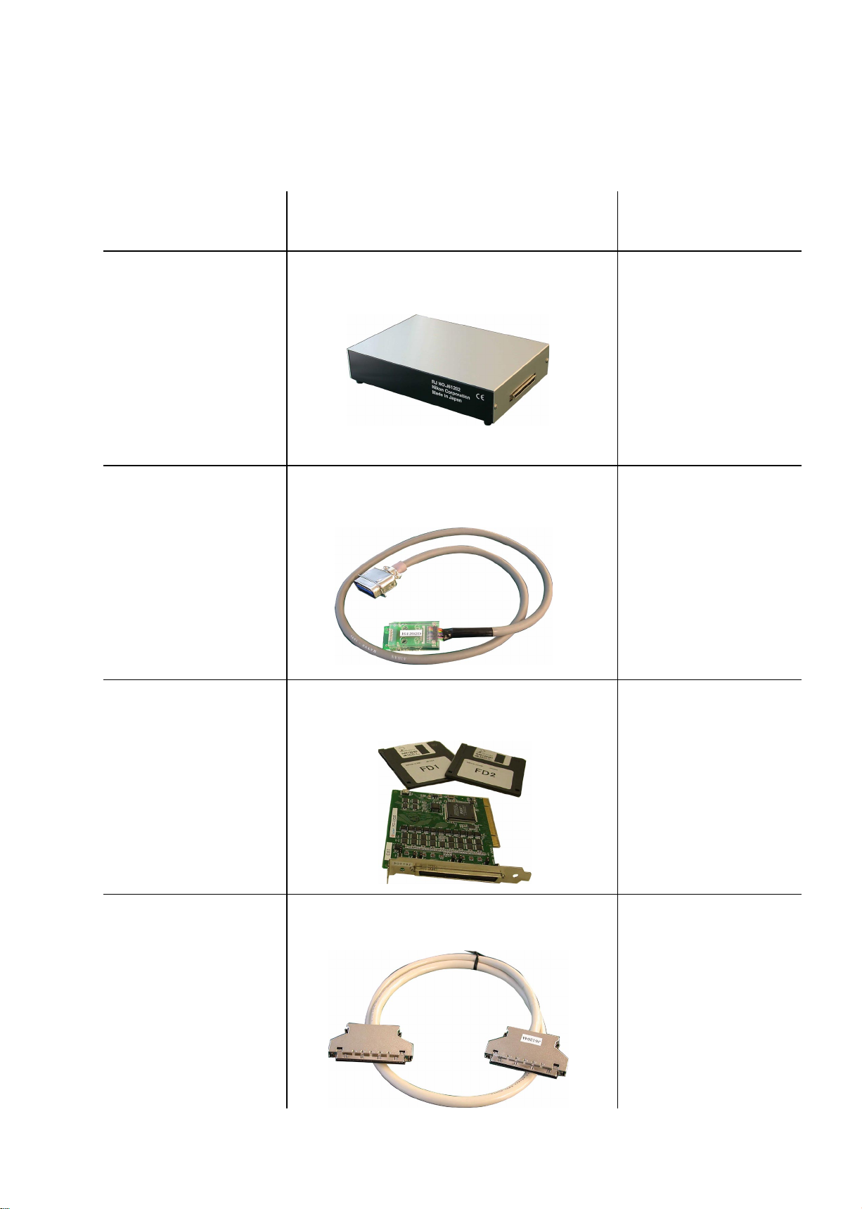
VAA31001-R.3651.A
※:新規工具
※:New tool
工具番号
Tool No.
※
J61202 レンズユニット検査工具
Lens unit checking tool
※
J61202F 接続コード
Connection cable for lens
名 称
Name
備 考
Remarks
FFD 点検調整用
For FFD inspection and
adjustment
FFD 点検調整用
For FFD inspection and
adjustment
※
J61204 デジタル通信ボード
PCI I/F board
J61204A 通信ボード用ケーブル
※
Connection cable for PC
FFD 点検調整用
For FFD inspection and
adjustment
FFD 点検調整用
For FFD inspection and
adjustment
- T3・ E5600 -
Page 100
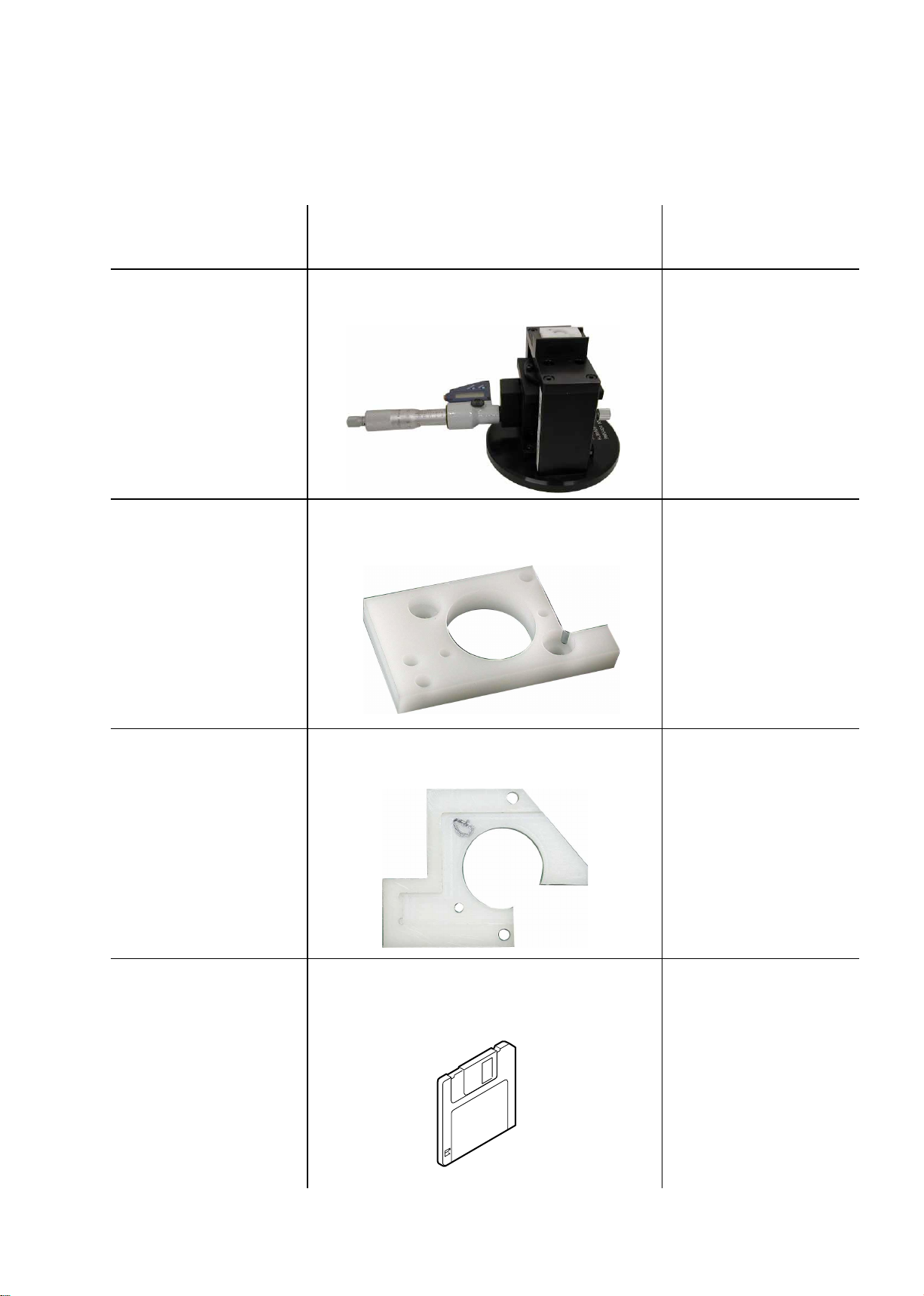
VAA31001-R.3651.A
※:新規工具
※:New tool
工具番号
Tool No.
J15327 FFD 調整用マイクロ台
※
Adjusting focus stand for APS
※
J15327A FFD 調整用マイクロ台アダプター
Adapter for J15327A
名 称
Name
備 考
Remarks
FFD 点検調整用
For FFD inspection and
adjustment
FFD 点検調整用
For FFD inspection and
adjustment
※
J15327D FFD 調整用マイクロ台アダプター
Adapter for J15327D
※
J65072 E4600/E5600 鏡筒駆動ソフト
E4600/E5600 lens unit checking program
FFD 点検調整用
For FFD inspection and
adjustment
FFD 点検調整用
For FFD inspection and
adjustment
- T4・ E5600 -
 Loading...