


NIKO P70N02LS Datasheet
NIKO-SEM
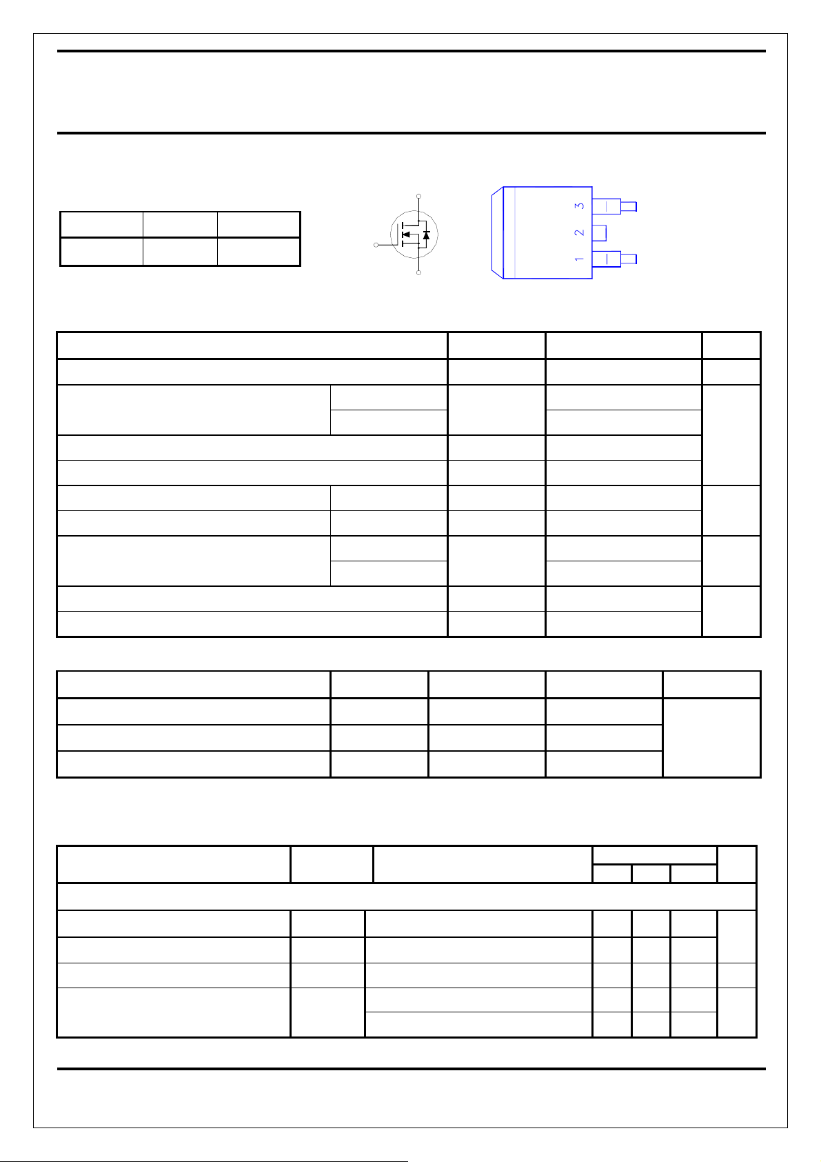
N-Channel Logic Level Enhancement
Mode Field Effect Transistor
P70N02LS
TO-263 (D2PAK)
D
PRODUCT SUMMARY
V
(BR)DSS
25
R
I
DS(ON)
7m
Ω
D
70A
G
1. GATE
2. DRAIN
3. SOURCE
S
ABSOLUTE MAXIMUM RATINGS (TC = 25 °C Unless Otherwise Noted)
PARAMETERS/TEST CONDITIONS SYMBOL LIMITS UNITS
Gate-Source Voltage VGS ±20 V
Continuous Drain Current
T
= 100 °C
C
Pulsed Drain Current1 I
I
D
170
DM
45
A
Avalanche Current IAR 60
Avalanche Energy L = 0.1mH EAS 140
mJ
Repetitive Avalanche Energy2 L = 0.05mH EAR 5.6
TC = 25 °C 65
TC = 25 °C 70
Power Dissipation
T
= 100 °C
C
Operating Junction & Storage Temperature Range Tj, T
P
D
-55 to 150
stg
38
W
°C
Lead Temperature (1/16” from case for 10 sec.) TL 275
THERMAL RESISTANCE RATINGS
THERMAL RESISTANCE SYMBOL TYPICAL MAXIMUM UNITS
Junction-to-Case
Junction-to-Ambient
Case-to-Heatsink
1
Pulse width limited by maximum junction temperature.
2
Duty cycle ≤ 1%
R
R
R
JC
θ
JA
θ
CS
θ
2.3
62.5
°C / W
0.6
ELECTRICAL CHARACTERISTICS (T
PARAMETER SYMBOL TEST CONDITIONS
= 25 °C, Unless Otherwise Noted)
C
LIMITS
MIN TYP MAX
UNIT
STATIC
Drain-Source Breakdown Voltage V
Gate Threshold Voltage V
Gate-Body Leakage I
Zero Gate Voltage Drain Current I
(BR)DSS
GS(th)
V
GSS
V
GS
V
DS
DS
VDS = 20V, VGS = 0V 25
DSS
= 20V, VGS = 0V, TJ = 125 °C 250
V
DS
1
= 0V, ID = 250µA
25
V
= VGS, ID = 250µA
1 1.5 3
= 0V, VGS = ±20V ±250 nA
A
µ
MAY-24-2001
NIKO-SEM
On-State Drain Current1 I
Drain-Source On-State
Resistance
1
Forward Transconductance1 g
N-Channel Logic Level Enhancement
Mode Field Effect Transistor
V
D(ON)
R
DS(ON)
V
fs
= 10V, VGS = 10V 70 A
DS
VGS = 10V, ID = 30A 7 9
V
= 7V, ID = 24A 8 10
GS
= 15V, ID = 30A 16 S
DS
DYNAMIC
P70N02LS
TO-263 (D2PAK)
mΩ
Input Capacitance C
Output Capacitance C
Reverse Transfer Capacitance C
Total Gate Charge2 Q
Gate-Source Charge2 Q
Gate-Drain Charge2 Q
Turn-On Delay Time2 t
Rise Time2 t
Turn-Off Delay Time2 t
Fall Time2 t
2700
iss
V
500
oss
rss
25
g
7
gs
gd
7
d(on)
r
d(off)
6
f
= 0V, VDS = 15V, f = 1MHz
GS
VDS = 0.5V
V
DS
≅ 30A, VGS = 10V, RGS = 2.5Ω
I
D
, VGS = 10V,
(BR)DSS
= 35A
I
D
= 15V, RL = 1Ω
200
11
7
24
pF
nC
nS
SOURCE-DRAIN DIODE RATINGS AND CHARACTERISTICS (TC = 25 °C)
Continuous Current IS 70
A
Pulsed Current3 I
Forward Voltage1 V
170
SM
I
SD
= IS, VGS = 0V 1.3 V
F
Reverse Recovery Time trr 37 nS
Peak Reverse Recovery Current I
RM(REC)
= IS, dlF/dt = 100A / µS
I
F
Reverse Recovery Charge Qrr 0.043
1
Pulse test : Pulse Width
2
Independent of operating temperature.
3
Pulse width limited by maximum junction temperature.
300 µsec, Duty Cycle
≤
≤
2%.
200 A
C
µ
REMARK: THE PRODUCT MARKED WITH “P70N02LS”, DATE CODE or LOT #
2
MAY-24-2001