

NIKO N1164 Datasheet
NIKO-SEM
5 Bit Programmable Synchronous Buck
Converter with Dual LDOs Controller
GENERAL DESCRIPTION
FEATURES
N1164
The N1164 is a 5 bit TTL-compatible input,
digital-to-analog (DAC) programmable, synchronous buck converter with dual LDOs
controller designed specifically to power the
Pentium ® II as well as the next generation of
P6 family or other high performance core
logic in desktop personal computer and file
servers CPU applications.
The N1164 switching section provides programmability of output voltage from 1.3V to
2.05V in 50mV steps and 2.0V to 3.5V in 100
mV increments and the linear sections use
external N-Channel power MOSFETs to
provide fixed output voltages of 1.5V for GTL
bus and 2.5V for clock.
The N1164 monitors all the output voltages.
A signal Power-Good signal is issued when
the core is within ±15% of the DAC setting.
Additional features are built-in over-voltage,
over-current protections for the core output
and logic compatible shutdown.
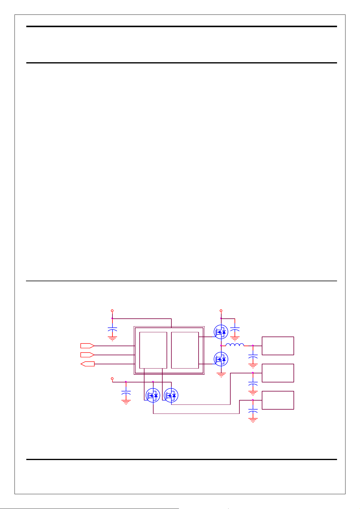
TYPICAL APPLICATION
Synchronous operation with high efficiency
z
TTL-compatible 5 bit DAC, output voltage
z
selection from 1.3V to 3.5V programmable
High current totem pole output, up to 2 A
z
for direct driving of the external N-Channel
power MOSFETs.
200 KHz fixed frequency internal oscillator
z
Fast transient response
z
Provides 2 regulated voltages, 1.5V and
z
2.5V for linear section
Power-Good output voltage monitor
z
Over-Voltage and Over-Current protection
zzzz
Logic level enable input
z
High performance and low cost solution
z
APPLICATIONS
Powering Pentium ® II, III or Deschutes,
z
K6 and other advanced processor
High power DC to DC controller with triple
z
output supplies
5V
+
VCORE
+
1.5V
GTC BUS
+
2.5V
CLOCK
+
ENABLE
VID 0~4
POWER-GOOD
12V
3.3V
+
LINEAR
SECTION
+
N1164
SWITCHING
SECTION
N1164, Motherboard Power Regulation for Computers
1
AUG-03-2001
NIKO-SEM
5 Bit Programmable Synchronous Buck
Converter with Dual LDOs Controller
ABSOLUTE MAXIMUM RATINGS
N1164
VCC to GND - 0.3V to 7V
z
BST to GND -0.3V to 15V
z
Thermal Resistance
z
Junction to Case,
Thermal Resistance
z
θ
JC
Junction to Ambient,
θ
JA
25 °C/W
80 °C/W
Operating Temperature
z
Range, TA
Operating Junction
z
Temperature Range, TJ
Storage Temperature
z
Range, T
Lead Temperature, T
z
STG
LEAD
(Soldering, 10 Seconds)
0 to 70 °C
0 to 125 °C
-65 to 150 °C
300 °C
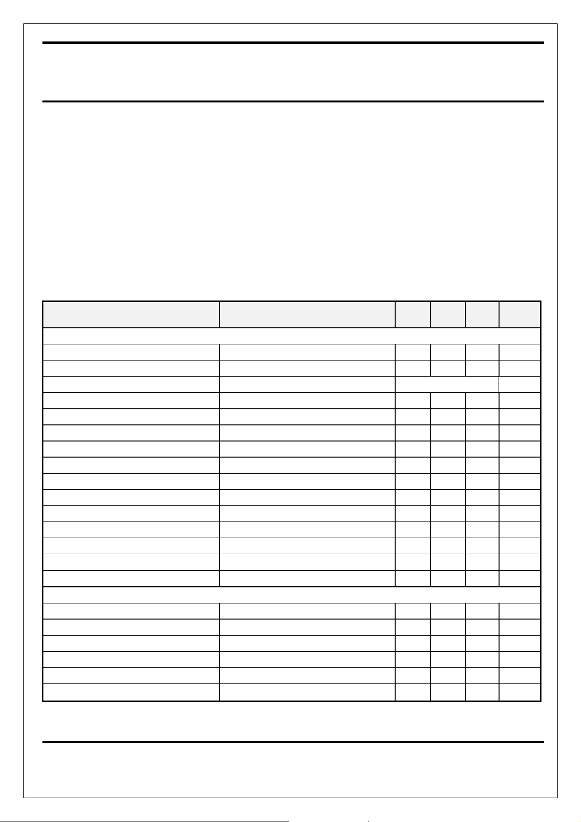
ELECTRICAL SPECIFICATIONS
<Unless specified: VCC = 4.75V ~ 5.25V, GND = PGND = 0V, V
OSENSE
PARAMETER CONDITIONS MIN TYP MAX UNITS
SWITCHING SECTION
Supply Voltage VCC 4.5 7 V
Supply Current VCC = 5.0V 8 15 mA
Output Voltage IO = 2A See Table 1.
Load Regulation IO = 0.3A to 15A 1 %
Line Regulation All VID Codes 0.5 %
Gain (AOL) V
OSENSE
Current Limit Voltage 55 70 85 mV
Oscillator Frequency 175 200 225 KHz
Oscillator Max Duty Cycle 90 95 %
Peak DH Sink/Source Current
Peak DL Sink/Source Current
BSTH - DH = 4.5V, DH - PGNDH = 2V
BSTL - DL = 4.5V, DL - PGNDL = 2V
OVP Threshold Voltage 120 %
OVP Source Current V
= 3.0V 10 mA
OVP
Power-Good Threshold Voltage 85 115 %
Dead Time 100 200 nS
= VO , 0mV < (CS+ - CS-) < 60mV, LDOV = 11.4V ~ 12.6V, TA = 25°C>
to VO 35 dB
1 A
1 A
LINEAR SECTIONS
Quiescent Current LDOV = 12V 5 mA
Output Voltage (LDO1) 2.45 2.500 2.55 V
Output Voltage (LDO2) 1.47 1.500 1.53 V
Load Regulation IO = 0 to 8A 1 %
Line Regulation 1 %
Output Impedance 1
KΩ
2
AUG-03-2001
NIKO-SEM
5 Bit Programmable Synchronous Buck
Converter with Dual LDOs Controller
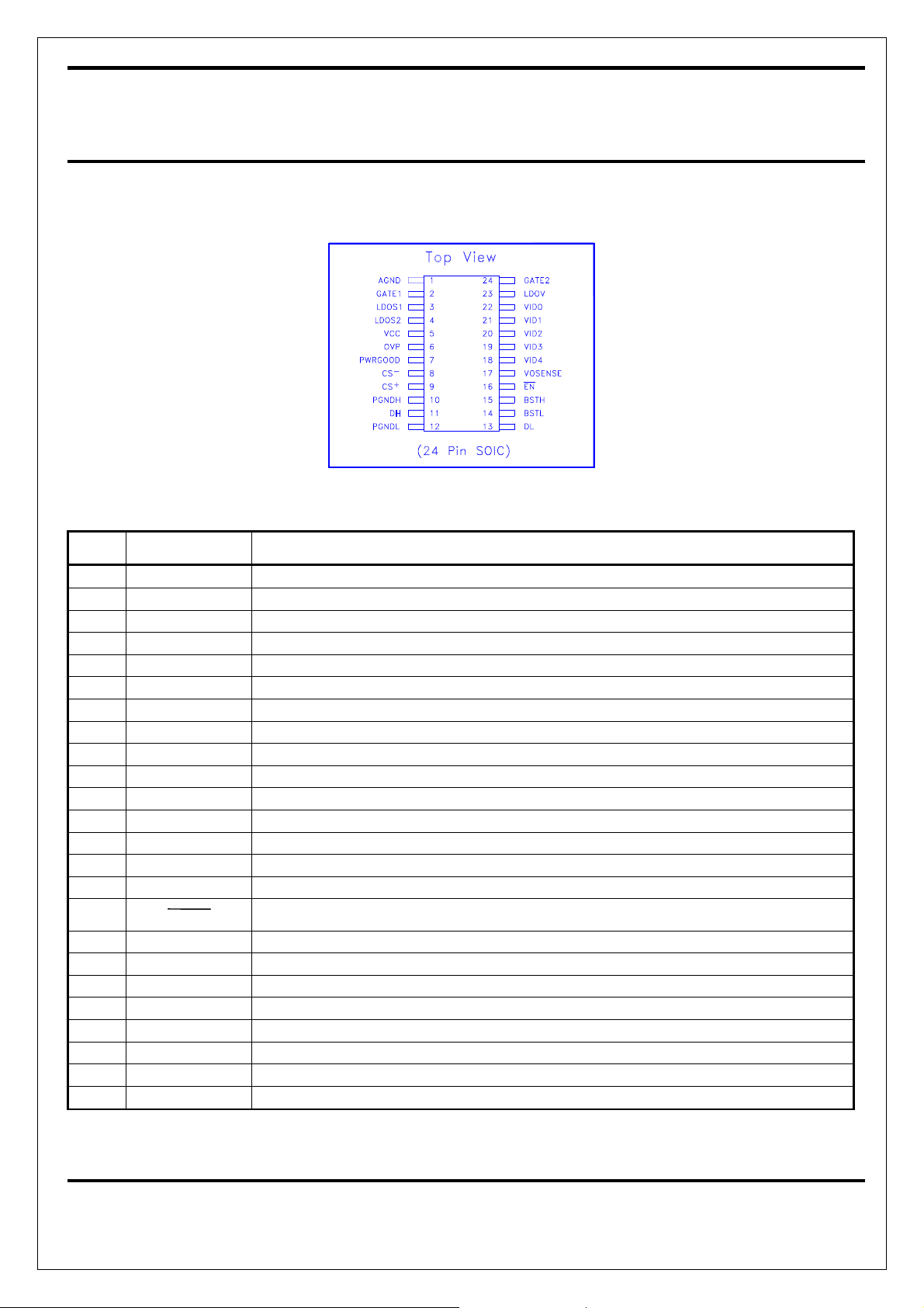
PIN CONFIGURATIONS
N1164
PIN DEFINITIONS
Pin # Pin Name Pin Function Description
1 AGND Small signal analog and digital ground
2 GATE1 Gate drive output LDO1
3 LDOS1 Sense input for LDO1
4 LDOS2 Sense input for LDO2
5 VCC Input voltage
6 OVP High signal out if VO>set point +20%
7 PWRGOOD* Open collector logic output, high if VO within 10% of set point
8 CS- Current sense input (Negative)
9 CS+ Current sense input (Positive)
10 PGNDL Power ground for high side switch
11 DH High side driver output
12 PGNDL Power ground for low side switch
13 DL Low side driver output
14 BSTL Supply for low side driver
15 BSTH Supply for high side driver
16
EN*
Logic low shuts down the converter; high or open for normal operation.
17 VOSENSE Top end of internal feedback chain
18 VID4* Programming input (MSB)
19 VID3* Programming input
20 VID2* Programming input
21 VID1* Programming input
22 VID0* Programming input (LSB)
23 LDOV +12V for LDO section
24 GATE2 Gate drive output LDO2
: All logic level inputs and outputs are open collector TTL compatible.
*
3
AUG-03-2001
 Loading...