

NIKO L1087N-3.3, L1087C-3.3, L1087C Datasheet
1
L1087 Series
SOT-89,TO-92
AUG-30-2001
0.8A Fixed and Adjustable Low Dropout
Linear Regulator (LDO)
NIKO-SEM
GENERAL DESCRIPTION
The L1087 Series are positive and low
dropout three-terminal voltage regulators
with 0.8A output current capability. These
devices are designed for use in low voltage
applications that offers lower dropout voltage and faster transient response.
These devices are fully protected against
over current faults, over temperature operation, reversed input polarity, reversed lead
insertion, transient voltage spike …etc.
On-Chips trimming the reference voltage to
1% and features the low dropout of maximum 1.45 volts.
The L1087 Series regulators offer fixed and
adjustable voltage options available in the
space saving SOT-89 & TO-92 package.
FEATURES
z
Fixed 3.3V or adjustable output voltage
z
Low dropout voltage
z
Low ground current
z
Fast transient response
z
Current & thermal lim iting
z
Line regulation: 0.5% typical
z
Load regulation: 0.5% typical
z
Available in SOT-89 & TO-92 package
APPLICATIONS
z
Low voltage micro-controllers
z
Battery Chargers
z
5V to 3.3V linear regulators
z
zz
z
Motherboard clock supplies
z
Post regulator for switching supplies
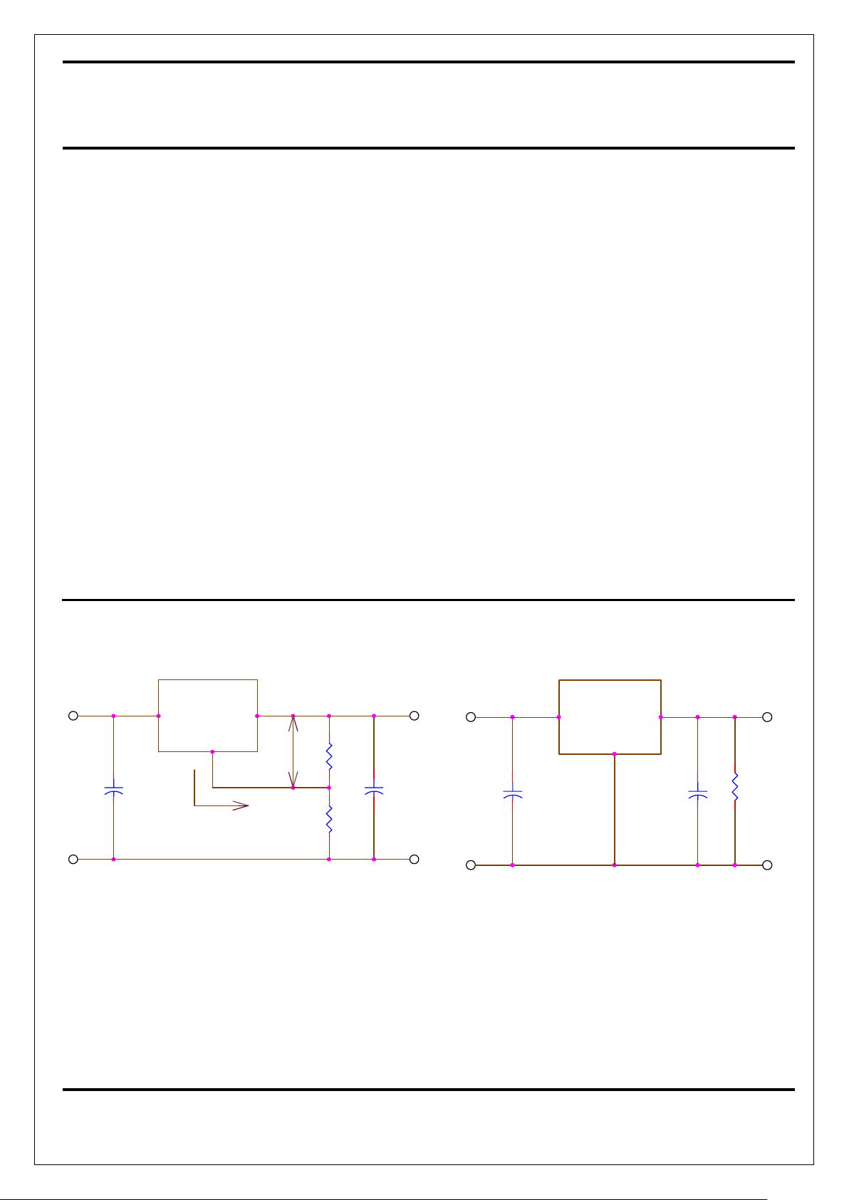
TYPICAL APPLICATION
- Basic Adjustable Regulator Circuit - - Fixed Voltage Regulator -
OUT
2. Cout required for stability.
+
Cout
10uF
Vin > 4.75V
GND
1. Cin needed if device is far from filter capacitors.
Vout = 3.3V
+
Cin
10uF
RL
L1087-3.3
IN
IN OUT
Iadj
ADJ
Vref
R2
+
Cin
10uF
1. Cin needed if device is far from filter capacitors.
L1087
2. Cout required for stability.
R1
Vo = Vref (1+R2/R1) + Iadj x R2
VoutVin
+
Cout
10uF
2
L1087 Series
SOT-89,TO-92
AUG-30-2001
0.8A Fixed and Adjustable Low Dropout
Linear Regulator (LDO)
NIKO-SEM
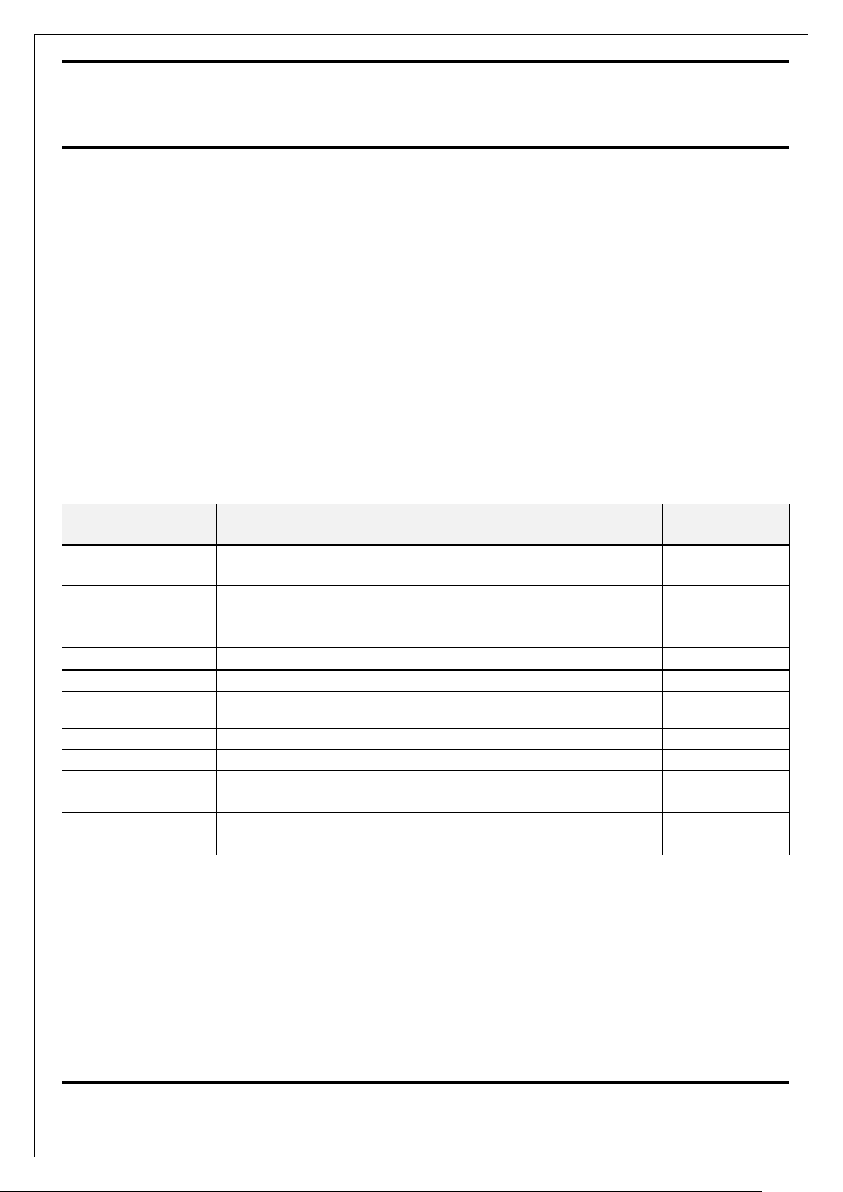
ABSOLUTE MAXIMUM RATINGS
z
Maximum Supply Voltage 15V*
z
Operating Junction
Temperature Range
0 to 125 °C
z
Power Dissipation
Internally
Limited
z
Storage Temperature
Range
-40 to 150 °C
z
Thermal Resistance
Junction to Case,
θ
JC
18 °C/W
z
Lead Temperature
(Soldering, 10 Seconds)
260 °C
z
Thermal Resistance
Junction to Ambient,
θ
JA
160 °C/W
* When considering short circuits to ground, the maximum input-to-output differential voltage shall not be allowed
greater than approximate 2~3V at values of supply voltage in excess of 10V, continuous short-circuits can exceed
the power dissipation ratings and cause eventual destruction.
ELECTRICAL CHARACTERISTICS
(Unless otherwise specified, TA = 25 °C)
Parameter
Symbol
Test Conditions Typical Limits
Reference Voltage
(Adjustable version)
V
REF
VIN = 5V, I
OUT
= 10mA
1.25V
1.23V
Min
1.27V
Max
Output Voltage
(Fixed version)
VO VIN = 5V, I
OUT
= 10mA
VO
0.98V
O(Min)
1.02V
O(Max)
Dropout Voltage VD
Δ
V
REF
= 1%, I
OUT
= 0.8A
1.2V 1.45V
Line Regulation REG
(LINE)
(V
OUT
+ 1.5V) ≤ V
IN
≤
15V, I
OUT
= 10mA
0.5% 2%
Load Regulation REG
(LOAD)
(V
IN -VOUT
) = 2V, 10mA ≤ I
OUT
≤ 0.8A
0.5% 2.5%
Minimum Load
Current
IO
1.5V ≤ (V
IN -VOUT
) ≤ 5.75V
10mA
Adjust Pin Current I
ADJ
55µA 100µA
Current Limit ICL VIN - V
OUT
= 2V 1.2A 0.9A (Min)
RMS Output Noise VN
0.003%
of V
OUT
Ripple Rejection
Ratio
R
A
f = 120Hz, C
ADJ
= 22µF for ADJ pin,
V
IN
= 5V, I
OUT
= 0.8A
72dB 60dB (Min)
 Loading...