

Nikko Alpha-220 Service Manual
......................................................
...........
........
CONTENTS
SPECIFICATIONS...................................................................
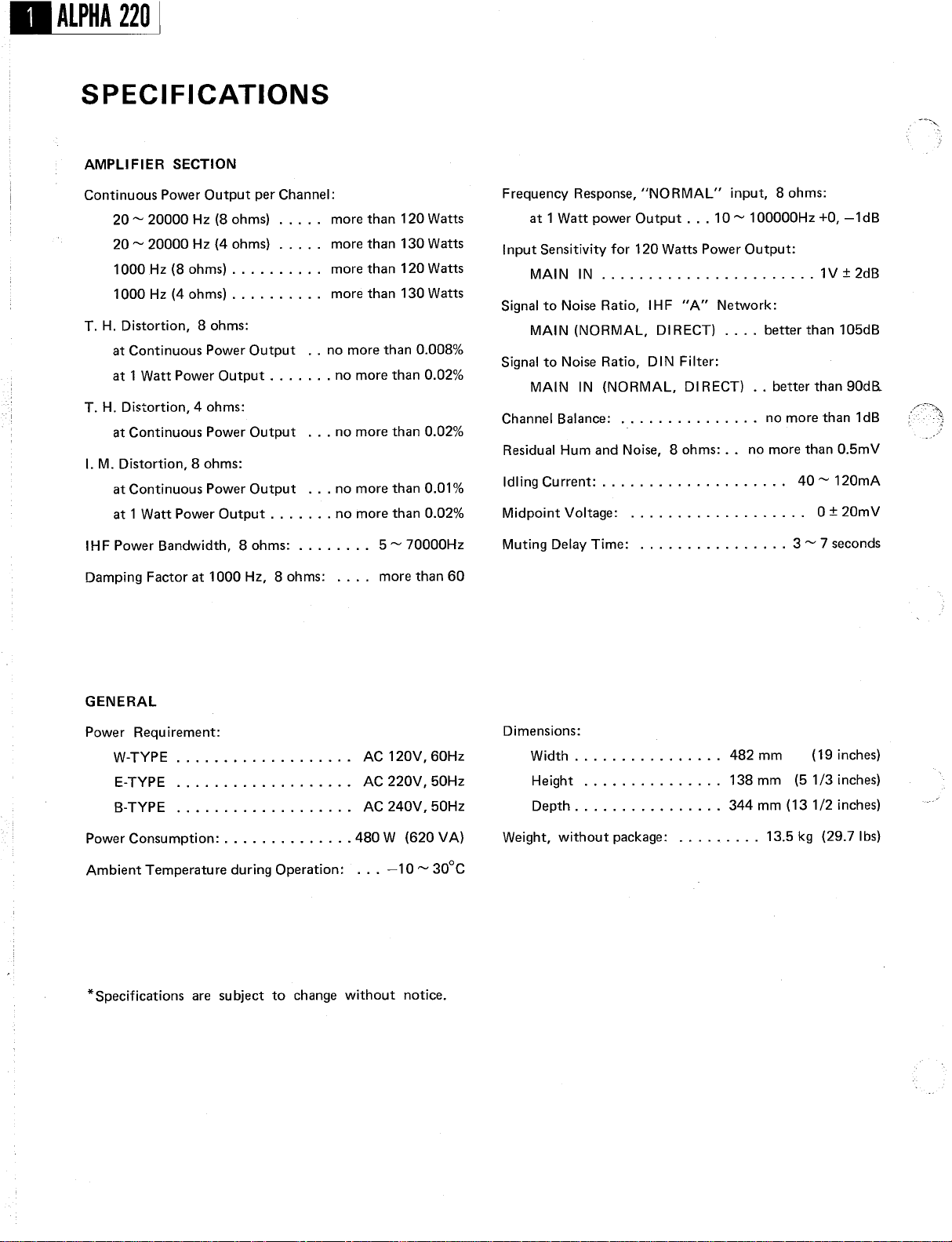
BLOCK DIAGRAM..................................................................
DISASSEMBLY .....................................................................
CIRCUIT DESCRIPTION ...................................,......................
PARTS LOCATION "
SCHEMATIC DIAGRAM
C. BOARD ..................................................................
4~6
.., 8
ALIGNMENT...................................................................
POWER TRANSISTORS MOUNTING ASSEMBLY .......................................
PARTS LIST...................................................................
SEMICONDUCTOR DATA
TRANSISTORS ...............................................................
FIELD EFFECT TRANSISTOR ...................................................
DIODES
ZENER DIODES "
INTEGRATED CIRCUITS .
, LED'S ............................................,.................
...................................................... 18
ALPHA 220
SPECIFICATIONS
AMPLIFIER SECTION
. . . . . . . . .
, "
, -
Continuous Power Output per Channel:
20 ~ 20000 Hz (8 ohms)
20 ~ 20000 Hz (4 ohms)
1000Hz(8ohms)..........
1000Hz(4ohms)..........
T. H. Distortion
at Continuous Power Output
at 1 Watt Power
T. H. Distortion
at Continuous Power Output
I. M. Distortion
at Continuous Power Output
at 1 Watt Power
IHF Power Bandwidth
Damping Factor at 1000 Hz
, 8 ohms:
. . no more than 0.
Output. . . . . . .
, 4 ohms:
. . . no more than 0.02%
, 8 ohms:
. . . no more than 0.
Output. . . . . . .
, 8 ohms: . . . . . . ..
, 8 ohms:
more than 120 Watts
more than 130 Watts
more than 120 Watts
more than 130 Watts
008%
no more than 0.02%
01%
no more than 0.
5 ~ 70000Hz
.... more
02%
than 60
Frequency Response
at 1 Watt power
NORMAL" input
Output. . . 10 ~
, 8 ohms:
100000Hz +0
Input Sensitivity for 120 Watts Power Output:
MAIN IN .......................
Signal to Noise Ratio
MAIN (NORMAL, DIRECT) ..,.
Signal to Noise Ratio
, I H F "
, DIN Filter:
MAIN IN (NORMAL,
Channel Balance:
Residual Hum and Noise
Idling Current:....................
Midpoint Voltage:
Muting Delay Time: ................
..,............ no
........,.......... 0:t20mV
Au Network:
DI RECT) .. better
, 8 ohms: .. no
better than 105dB
more than 0.
1dB
1V:t2dB
than 90dB.
more than 1dB
5mV
40~120mA
3~7seconds
GENERAL
Power Requirement:
TYPE .................,. AC120V
TYPE ..,................ AC220V
TYPE ................... AC240V
Power Consumption: . . . . .
Ambient Temperature during Operation: ... -
* Specifications are su
bject to change
480 W (620 VA)
without notice.
60Hz
50Hz
50Hz
1 0 ~ 30
Dimensions:
Width................
Height ...............
Depth................
, without package:
Weight
482mm
(19 inches)
138mm (51/3inches)
344mm(131/2inches)
......... 13.5 kg (29.
7Ibs)
::I=-
r--
::I=-
c:)
(")
--,
ASS'
LEVEL
POWER
809
REGULATR + 125V
LED DRIVE
0808
r=-
729
0727
COMPo
THERMAL INDICATOR
:t:-
:t:-
IND
"V' POWER INO
"V' PROTECTION
HEAD-
PHONES
..JACK
Lt:.
DC
DETECT I
DETECT
OVERLOAD
LED DRIVER
SPEAKERS
RELAY DRIVE
PROTECTOR,
MUTING &
SPEAKERS
RELAY
TO POWER TRANSISTORS
080 I ~0807
": 58.
POWER SUPPLY
POWER SWITCH
. SW I
~~ ~~~ ~ - - - - -" - - - - - - "- - - - - -
---- -----------------------------
- - - - - - ~ - - - - -
; 1
725
DRIVER '
BIAS &
VARIABLE
PRE DRIVER
WITH CURRENT
MIRROR LIMITER 0723
~~V
705
2ND STAGE
070 I 0703
FIRST STAGE
I +
1:--
3) I
TO DRIVE AMP.
721
, 717 I . .
, 709 0715
711713 719
DC-SERVO
NFB
(DUALFET)
I - 0707
L -----
, 712
, 7 10
, 720, 722
726
, 704, 706
RIGHT CH. TRANSISTORS
0702
0714, 7 I 6, 718
C4.
POWER
TRANSFORMER
AC LINE
(3)'
SW3:
DIRECT
- NO
...,
INPUT
J:1
II
ALPHA 220
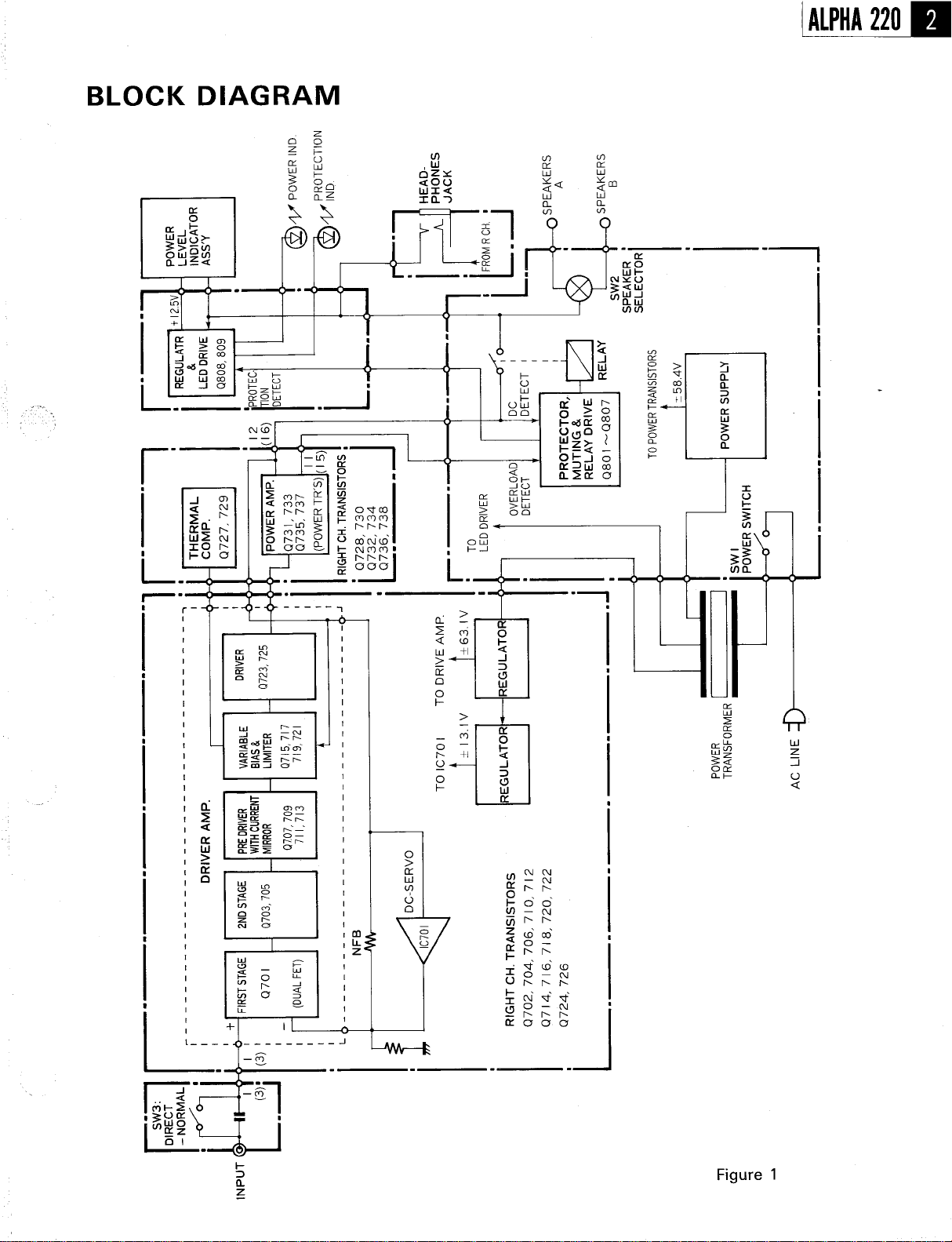
DISASSEMBLY
CABINET COVER REMOVAL
Remove four tapping screws from the top
Remove four
screws from both
sides of the unit.
Lift the cabinet cover away from the unit.
BOTTOM PLATE REMOVAL
Remove nine tapping screws from the bottom
unit as shown in Photo 1. (#1
- #9)
Lift the bottom plate away from the unit.
of the unit.
of the
FRONT PANEL REMOVAL
Remove three tapping screws (#1
- #3) from the
side of the unit as shown in Photo 2.
Similarly remove three tapping screws from the right
side of the unit.
Remove the front panel away from the unit by
it forward.
POWER TRANSFORMER REMOVAL
Remove the cabinet cover and the
Disconnect all the cables from the power transformer.
Remove four nuts (#1
- #4) from the
bottom plate.
chassis as shown
in Photo 3.
Lift the power transformer away from the unit.
left
pulling
Photo
Photo 2
Photo 3
CIRCUIT DESCRIPTION
I ALPHA 220
NI KKO'
Hi-
s ALPHA 220
tT power transistors
, adopting latest
, is of a design introducing a variable
bias circuit (non-switching circuit), a DC
devices such as
servo circuit and
other most advanced techniques.
For details
and page 8 "
The following are
and devices.
, refer to
page 2 "
SCHEMATIC DIAGRAM"
explanations of the main
BLOCK DIAGRAM"
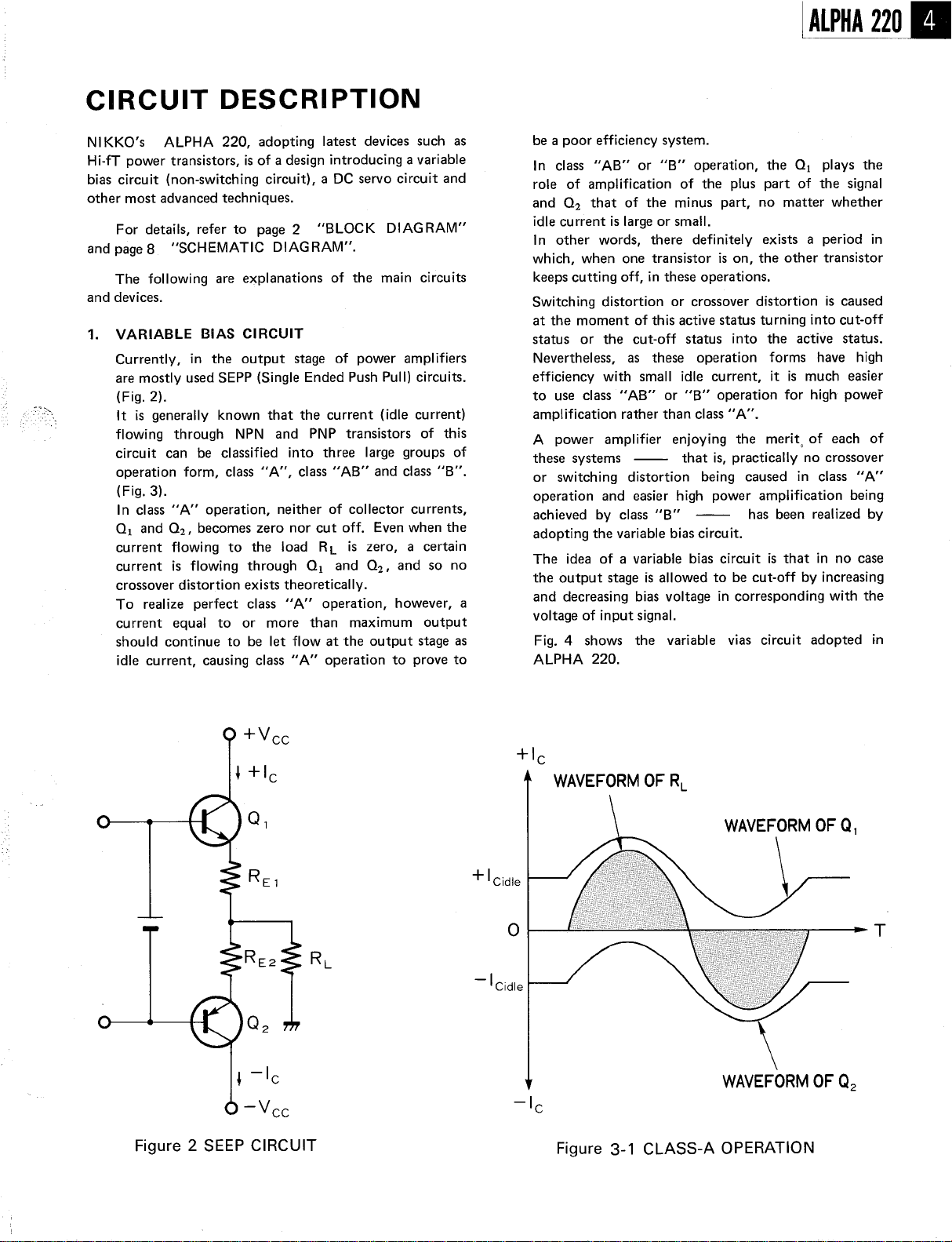
VARIABLE BIAS CIRCUIT
Currently, in the output
stage of power
are mostly used SEPP (Single Ended Push Pull) circuits.
(Fig. 2).
It is generally
flowing through NPN and PNP
circuit can be
operation form,
(Fig. 3).
In class "A" operation
01 and O2, becomes zero
current flowing to the load
current is flowing through 01
known that the current (idle
transistors of this
classified into three large
class " , class "AB" and class "
, neither of collector currents
nor cut off. Even when the
RL is zero
and O2, and so no
, a certain
crossover distortion exists theoretically.
real ize
To
current equal to or
perfect class
more than maximum
should continue to be let
idle current, causing class
" A" operation
flow at the output stage as
" A" operation to
, however
circuits
amplifiers
current)
groups of
, a
output
prove to
be a poor efficiency system.
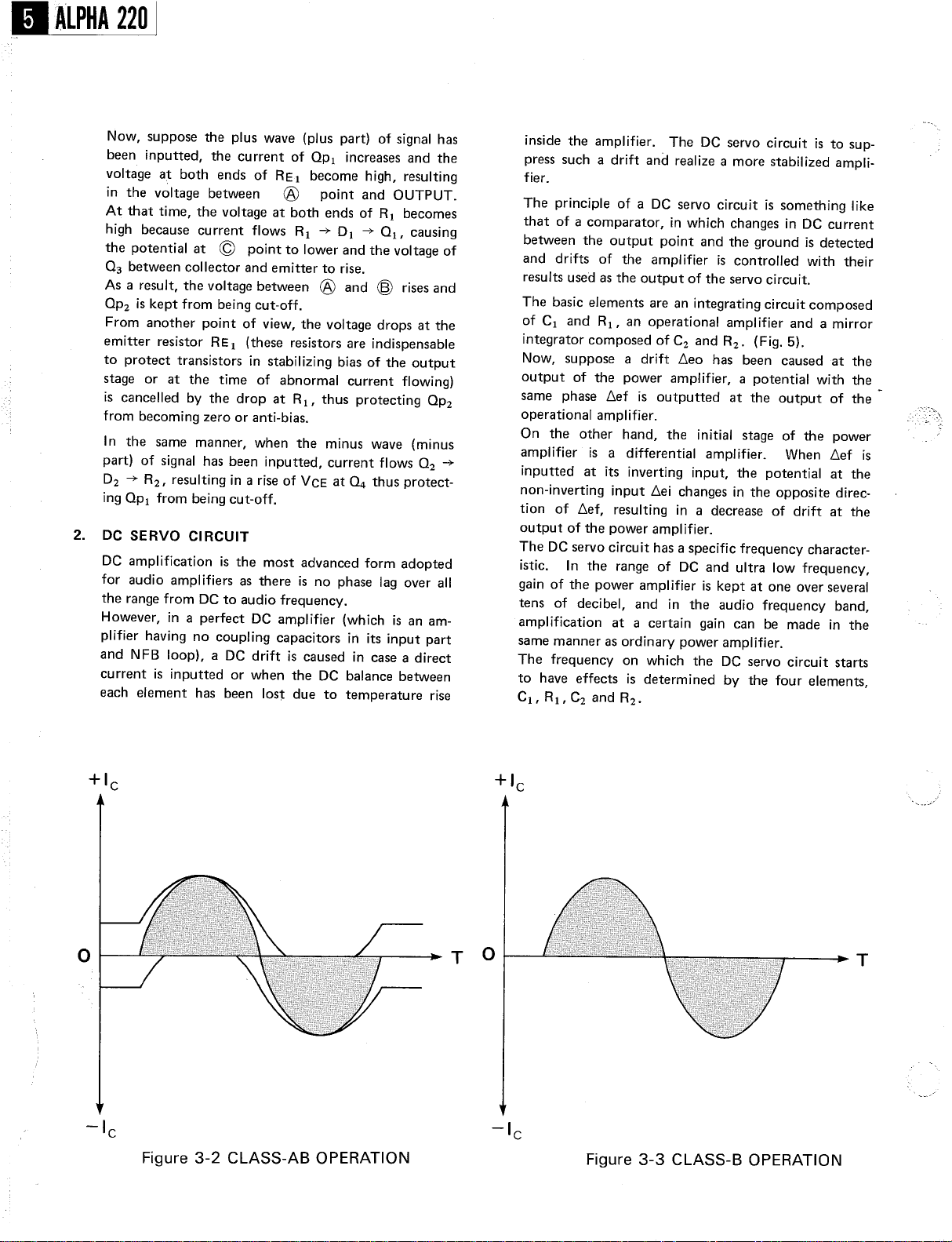
In class "AB" or "
role of amplification of the plus part of the
B" operation
and O2 that of the minus part
, the 01
, no matter whether
plays the
signal
idle current is large or small.
I n other words
which, when one transistor is on
keeps cutting off
Switching distortion or
at the moment of this active
status or the cut-off
Nevertheless
efficiency with small idle current
to use
class "
, there definitely exists a period in
, the other transistor
, in these operations.
crossover distortion is caused
status turning into cut-off
status into the
, as
these operation forms have
active status.
, it is much easier
AB" or "B" operation for high power
high
amplification rather than class "
power amplifier enjoying the merit
these systems that is
or switching distortion being caused in
operation and
achieved by
easier high power amplification
class "
B"
, practically no crossover
has been realized by
, of each of
class "
being
adopting the variable bias circuit.
The idea of a
variable bias circuit is that in no
the output stage is allowed to be cut-off by
case
increasing
and decreasing bias voltage in corresponding with the
voltage of input signal.
Fig. 4 shows the
variable vias circuit adopted in
ALPHA 220.
+Vee
RE2
Figure 2 SEEP CIRCUIT
eidle
eidle
WAVEFORM OF R
Figure 3-
1 CLASS-
WAVEFORM OF QI
WAVEFORM OF Q2
A OPERATION
ALPHA
220
Now
, suppose the plus wave (plus part) of
been inputted
voltage at both ends of
in the voltage between
At that time
, the current of Qp1
RE 1 become high
point and
CBJ
, the voltage at both ends of
increases and the
high because current flows R1 -+ D1 -+ Q1,
the potential at
point to lower and the voltage of
(Q
03 between collector and emitter to rise.
As a result
Qp2 is kept from being cut-off.
From another point of view
emitter resistor RE
to protect
stage or at the time of abnormal
is cancelled by the drop at R
from becoming zero or anti-
In the same manner
part) of signal has been inputted
D2 -+ R2, resulting in a rise of
, the voltage between
CBJ
and
, the voltage drops at the
1 (these resistors
transistors in stabilizing bias of the output
1, thus protecting Qp2
bias.
, when the minus wave (minus
, current flows
VCE at Q4 thus protect-
ing Qp1 from being cut-off.
DC SERVO CIRCUIT
DC amplification is the most
for audio
amplifiers as there is no
advanced form adopted
phase lag over all
the range from DC to audio frequency.
However
, in a perfect
DC amplifier (which is an am-
plifier having no coupling capacitors in its input part
and N FB loop), a DC drift is
current is inputted or
each element has been
when the DC
caused in case a direct
balance between
los~ due to
temperature rise
signal has
, resulting
OUTPUT.
R1 becomes
causing
rises and
are indispensable
current flowing)
Q2 -+
inside the amplifier. The
press such a drift and
DC servo circuit is to
realize a more stabilized ampli-
sup-
fier.
The principle of a
that of a comparator
between the output point and the ground
and drifts of
DC servo circuit is something like
, in which changes in DC current
the amplifier
is controlled with their
is detected
results used as the output of the servo circuit.
The basic elements are an integrating circuit composed
of C1 and R1' an
operational amplifier and a mirror
integrator composed of C2 and R2. (Fig. 5).
Now
, suppose a
output of the power amplifier
same phase llef
drift
lleo
has been caused at the
, a potential with the
is outputted at the output of the
operational amplifier.
On the
amplifier is a
inputted at its
non-
tion of llef
other hand
inverting input llei changes in the opposite direc-
, resulting in a decrease of
, the
initial stage of the
differential amplifier.
inverting input
, the potential at the
power
When llef
drift at the
output of the power amplifier.
The DC servo circuit has a specific frequency character-
istic. In the range of
gain of the power amplifier is kept at one over
tens of decibel
amplification at a
, and in the audio frequency band
DC and ultra low
certain gain can be
frequency,
several
made in the
same manner as ordinary power amplifier.
The frequency on which the DC
to have
C1,
effects is
R1,
C2andR2.
determined by the four elements
servo circuit starts
Figure 3- 2 CLASS-
AB OPERATION
Figure 3-
3 CLASS-
B OPERATION
 Loading...