

A
g
查询PVD75-6供应商
TENTATIVE
PIM MODULE
MODULE 7.5KW 200V
MODULE MODULE
7.5KW 200V
7.5KW 200V7.5KW 200V
PVD75
PVD75----6666
PVD75PVD75
Futures : Integrated in 3Phase Diode Bridge, Thyristor Switch, Inverter, Brake, and Snubber
For 7.5kw 200V Inverter
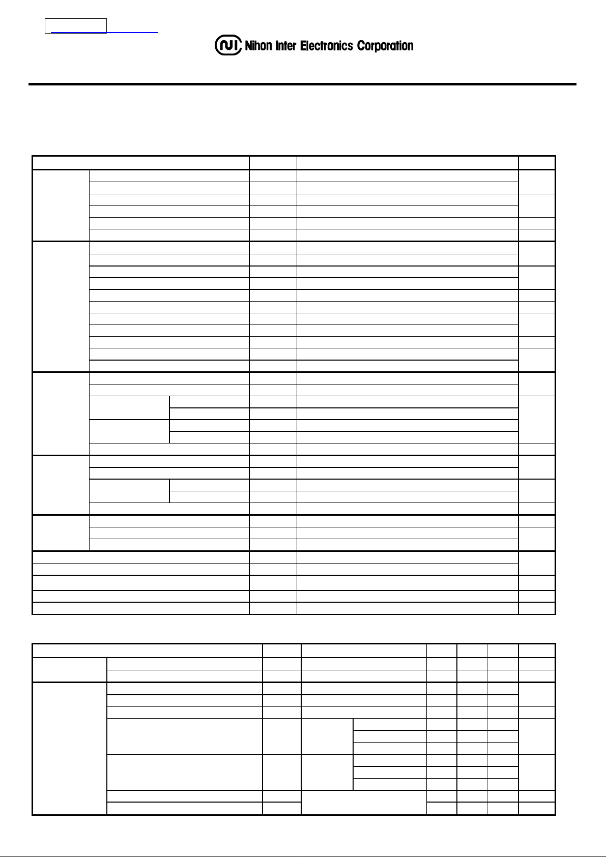
MAXMUM RATINGS
(Tc=25°C)
pproximate Weight : 400
Item Symbol Rated Value Unit
Repetitive Peak Reverse Voltage V
3 Phase
Rectification
Diode
Non-Repetitive Peak Reverse Voltage V
Average Rectified Out –Put Current I
Surge Forward Current I
I Squared t I2t 3200 A2s
Critical Rate of Fall of Forward Current -di/dt 160(@ :I
Repetitive Peak Off-State Voltage V
Non-Repetitive Peak Off-State Voltage V
Average Rectified Out-Put Current I
Surge Forward Current I
Switch
Thyristor
I Squared t I2t 3200 A2s
Critical Rate Of Rise Of Turn-On Current di/dt 100 A/µs
Peak Gate Power PGM 5
Average Gate Power P
Peak Gate Current IGM 2 A
Peak Gate Voltage VGM 10
Peak Gate Reverse Voltage V
Collector-Emitter Voltag e V
Gate-Emitter Voltage V
Inverter
IGBT
Collector Current
Forward Current
DC IC 75
1
I
ms
DC IF 75
1
I
ms
Collector Power Dissipation P
Collector-Emitter Voltag e V
Brake
IGBT
Gate Emitter Voltage V
Collector Current
DC IC 30
1ms I
Collector Power Dissipation P
Snubber
Diode
Repetitive Peak Reverse Voltage V
Forward Current, DC IF 15
Surge Forward Current I
Operating Junction Temperat ure Range Tjw
Storage Temperature R ange Tstg
Isolation Voltage(Terminal to Base) Viso
Isolation Resistance(Terminal to Base, @DC=500V) Riso 500 M.ohm
Mounting Torque(Module Base to Heatsink) Ftor (M4), 1.4 N·m
800
RRM
900
RSM
75
O(AV)
800
FSM
=25A, VR=500V) A/µs
FM
800
DRM
900
RSM
75
O(AV)
800
TSM
GM(AV)
5
RGM
600
CES
+/- 20V
GES
150
CP
150
FM
300 W
C
600
CES
+/- 20V
GES
60
CP
178 W
C
600 V
RRM
150
FSM
1
-40 to +150°C(notes:+125 °C > Can not be biased.)
-40 to +125°C
W
°C
2500(@AC, 1minute), 3000(@AC, 1second) V
ELECTRICAL CHARACTERISTICS
(Tc=25°C Unless otherwise noted)
Characteristic Symbol Test Condition Min. Typ. Max. Unit
3 Phase
Rectification Diode
Switch Thyristor
Peak Reverse Current *1 IR
Peak Reverse Voltage *1 V
Peak OFF-State Current IDM
Peak Reverse Current IRM
Tj=150°C, V
IF=80A - - 1.40
F
Tj=125°C, V
Tj=125°C, V
RM=VRRM
DM=VDRM
RM=VRRM
- - 10 mA
µA
- - 50
- - 50
mA
Peak On-State Voltage VTM IT=80A - - 1.4 0 V
=6V
V
Gate Current to Trigger IGT
Gate Voltage to Trigger VGT
Gate Voltage to Non-Trigger VGD 0.25 - - V
Critical Rate Of Rise Of Off-State Voltage dv/dt
D
I
=1A
T
V
=6V
D
I
=1A
T
Tj=125°C, V
Tj=-40°C
Tj=25°C
Tj=125°C
Tj=-40°C
Tj=25°C
Tj=125°C
=2/3V
D
DRM
- - 200
- - 100
mA
- - 50
- - 40
- - 25
- - 20
500 - - V/µs
V
A
V
A
V
V
A
V
A
A
V
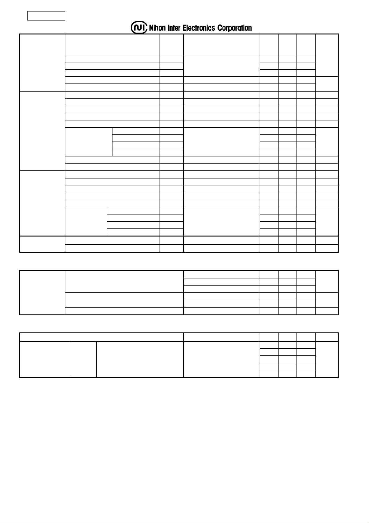
TENTATIVE
Tj=125°C, V
Turn-Off Time tq
V
-di/dt=20A/µs
Switch Thyristor
Turn-On Time tgt - 6 Delay Time td - 2 Rise Time tr
Tj=25°C, V
I
-di
Latching Current IL - 100 -
Inverter
IGBT
Holding Current I
Collector-Emitter Out-Off Current I
Gate-Emitter Leakage Current I
Collector-Emitter Saturation Voltage V
Gate-Emitter Threshold Voltage V
Input Capacitance Cies VCE=10V,VGE=0V,f=1MHz - 7500 - pF
Rise Time tr - 0.15 0.30
Switching Time
Turn-On Time ton - 0.25 0.40
Fall Time tf - 0.20 0.35
Turn-Off Time toff
- 80 -
H
VCE=600V,VGE=0V - - 1.0 mA
CES
VGE=+/- 20V,VCE=0V - - 0.5
GES
IC=75A,VGE=15V - 2.1 2.6 V
CE(sat)
VCE=5V,IC=75mA 4.0 - 8.0 V
CE(th)
V
R
R
V
Peak Forward Voltage VF IF=75A - 1.9 2.4 V
Brake
IGBT
Reverse Recovery Time trr
Collector-Emitter Cut-Off Current I
Gate-Emitter Leakage Current I
Collector-Emitter Saturation Voltage V
Gate-Emitter Threshold Voltage V
Input Capacitance Cies VCE=10V,VGE=0V,f=1MHz - 4000 - pF
Rise Time tr - 0.15 0.3
Switching Time
Turn-on Time ton - 0.25 0.4
Fall Time tf - 0.20 0.35
Turn-off Time t
I
VCE=600V,VGE=0V - - 1.0 mA
CES
VGE=+/- 20V,VCE=0V - - 0.5
GES
IC=30A,VGE=15V - 2.0 2.5 V
CE(sat)
VCE=5V,IC=30mA 4.0 - 8.0 V
GE(th)
V
R
R
V
off
Peak Forward Voltage VF IF=15A - - 2.5 V Snubber
Diode
Reverse Recovery Time
trr I
*1: per 1arm
ELECTRICAL CHARACTERISTICS (Tc=25°C Unless otherwise noted)
25°C
Resistance
Thermister
B-Value
75°C
125°C
25°C/50°C
25°C/85°C
Thermal Time Constant - 10 - s
THERMAL CHARACTERISTICS
Characteristic Test Condition Min. Typ. Max. Unit
3 Phase Rectification Diode - - 0.75
Switch Thyristor - - 0.55
Inverter IGBT - - 0.42
Inverter Free Wheeling Diode - - 0.90
Per :1 arm.
Brake IGBT
Thermal Impedance
R
th(j-c)
Junction to Case
=2/3V
D
=100V, dv/dt=20V/µs
RM
=2/3V
D
=200mA
G
/dt=0.2A/µs
G
= 300V
CC
= 2 ohm
L
= 10 ohm
G
= +/- 15V
GE
=75A,VGE=-10V, di/dt=75A/µs
F
= 300V
CC
= 10 ohm
L
= 15 ohm
G
= +/- 15V
GE
=15A, di/dt=50A/µs
F
DRM
DRM
- 100 -
- 4 -
- 0.45 0.7
- 0.15 0.25
- 0.45 0.7
- - 0.3
- 5.00 -
- 0.97 -
k. ohm
- 0.27 -
- 3375 -
- 3420 -
°C/W
- - 0.70
µs
mA
µA
µs
µs
µA
µs
µs
K

TENTATIVE
PVD75-6 OUTLINE DRAWING
(Dimensions in mm)
CIRCUIT
 Loading...