

A
g
查询PHMB300B12供应商
MODULE
IGBT
MODULE Single 300A 1200V
MODULE MODULE
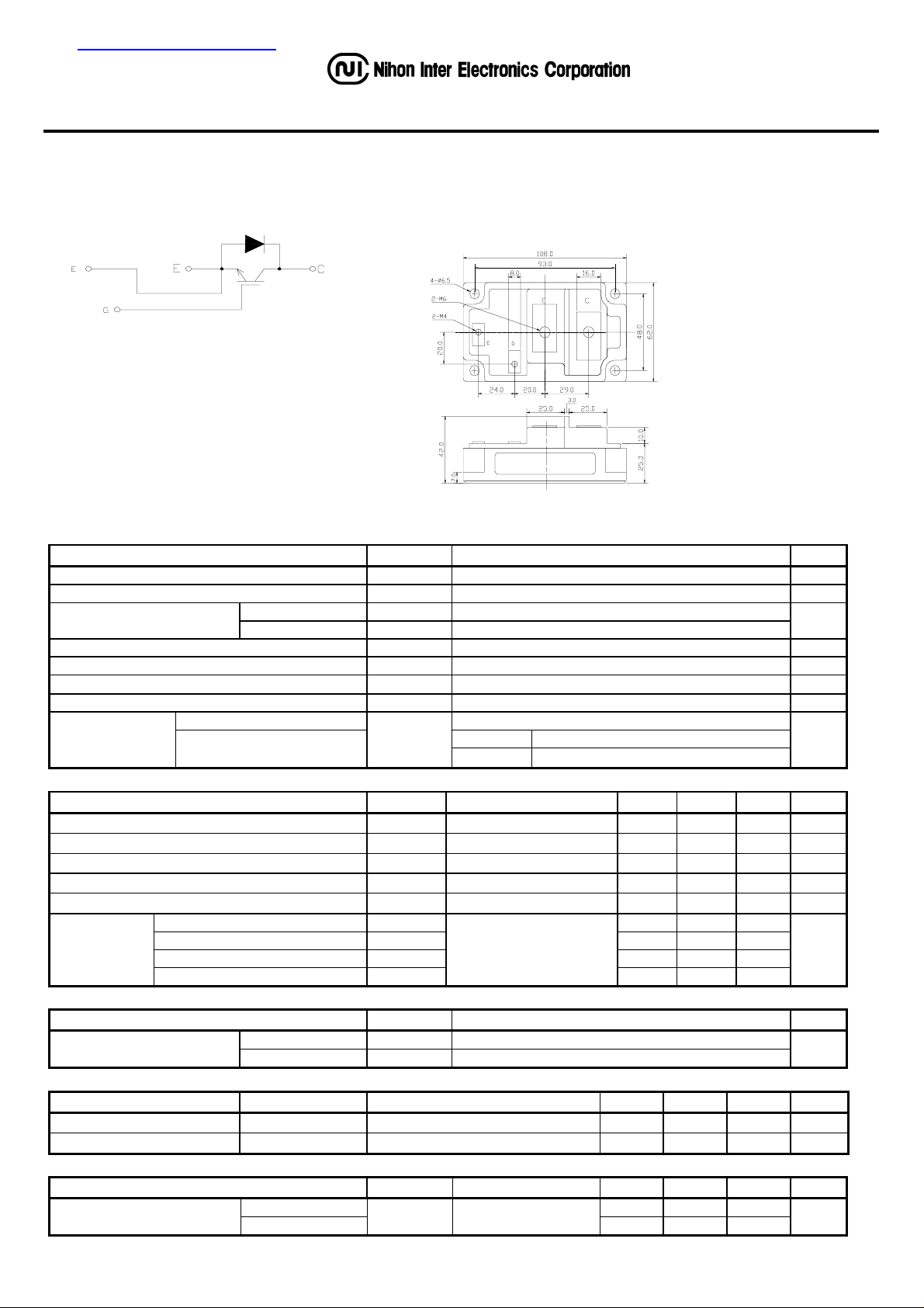
CIRCUIT OUTLINE DRAWING
Single 300A 1200V
Single 300A 1200VSingle 300A 1200V
PHMB300B12
PHMB300B12
PHMB300B12PHMB300B12
Dimension(mm)
MAXMUM RATINGS
(Tc=25°C)
pproximat e Weight : 6 50
Item Symbol PHMB300B12 Unit
Collector- Emitter V oltage V
Gate - Emitter Voltage V
Collector Current
Collector Power Dissipation PC 1600 W
Junction T emperature R ange Tj -40 to +150 °C
Storage Temp erature Range T
Isolation Voltage Terminal to Base AC, 1 min.) V
Module Base t o Heatsink 3
Mounting Torqu e
Bus Bar to Main Terminals
DC IC 300
1 ms I
1200 V
CES
+/ - 20 V
GES
600
CP
-40 to +125 °C
stg
2500 V
ISO
F
TOR
M4 1.4
M6
3
A
N•m
ELECTRICAL CHARACTERISTICS (Tc=25°C)
Characteristic Symbol Test Condition Min. Typ. Max. Unit
Collector-Emitter Cut-Off Current I
Gate-Emitter Leakage Current I
Collector- Emitter S aturation V oltage V
Gate-Emitter Threshold Voltage V
Input Capacitance Cies VCE=10V,VGE=0V,f=1MHz - 25000 -
Rise Time tr - 0.25 0.45
Switching Tim e
Turn-on Time ton - 0.40 0.70
Fall Time tf - 0.25 0.35
Turn-off Time t
VCE=1200V,VGE=0V - - 6.0
CES
VGE=+/- 20V,VCE=0V - - 1.0
GES
IC=300A,VGE=15V - 1.9 2.4
CE(sat)
VCE=5V,IC=300mA 4.0 - 8.0
GE(th)
V
= 600V
CC
R
= 2 ohm
L
RG= 1.3 ohm
off
VGE= +/- 15V
- 0.80 1.10
mA
µA
V
V
pF
µs
FREE WHEELING DIODES RATINGS & CHARACTERISTICS (Tc=25°C)
Item Symbol Rated Value Unit
Forward Current
DC IF 300
1 ms I
600
FM
A
Characteristic Symbol Test Condition Min. Typ. Max. Unit
Peak Forward Voltage VF I
Reverse Recovery Time trr
I
F
=300A,VGE=0V - 1.9 2.4
F
=300A,VGE=-10V,di/dt= 600A/µs
- 0.20 0.30
V
µs
THERMAL CHARACTERISTICS
Characteristic Symbol Test Condition Min. Typ. Max. Unit
Thermal Imp edance
IGBT - - 0.086
DIODE
R
Junction to Cas e
th(j-c)
- - 0.16
°C/W

PHMB300B12
600
500
(A)
400
C
300
200
Coll ector Current I
100
0
0246810
16
14
(V)
CE
12
10
Fig.1- Output Characteristics
VGE =20V
15V
12V
Col lector to E m itter V ol ta g e VCE
Fig.3- Collector to Emitter On Voltage
vs. Gate to Emitter Voltage
IC=150A
300A
600A
(Typical)
(V)
(Typical)
TC=25℃
C=125℃
T
10V
9V
8V
7V
(V)
CE
16
14
(V)
CE
12
10
8
6
4
Coll ector to Emitter V oltage V
2
0
800
700
600
500
Fig .2- Collector to Emitter On Voltage
vs. Gate to Emitter Voltage
IC=100A 600A
300A
0 4 8 12 16 20
Gate to Em itter Voltag e VGE
Fig.4- Gate Charge vs. Collector to Emitter Voltage
RL=2Ω
=25℃
T
C
(Typical)
TC=25℃
(V)
(Typical)
16
14
Gate to Emitter Voltage V
12
10
8
6
4
Coll ector to Emitter V oltage V
2
0
0 4 8 12 16 20
Gate to Em itter Voltag e VGE
(V)
400
300
200
Collector to Emitter Voltage V
100
0
0 400 800 1200 1600 2000 2400
Total Gate Ch arge Qg
VCE=600V
400V
200V
(nC)
8
6
GE
(V)
4
2
0
Fig .5- Capaci tance vs . Collector to Emitter Voltage
100000
50000
20000
10000
(pF)
5000
2000
1000
Capacitance C
500
Cies
Coes
Cre s
(Typical)
VGE=0V
f=1 MH
Z
TC=25℃
(μ s)
Switching Time t
200
100
0.1 0.2 0.5 1 2 5 10 20 50 100 200
Collector to Emitter Voltage VCE
(V)
Fig.6- Collector Current vs. Switching Time
1.4
1.2
1
tOFF
0.8
tf
0.6
0.4
0.2
ON
t
r
t
0
0 50 100 150 200 250 300
Collector Current IC
(A)
(Typical)
VCC=600V
R
G=1.3 Ω
V
=± 15V
GE
T
C=25℃

PHMB300B12
Fig.7- Series Gate Impedance vs. Switching Time
10
VCC=600V
I
C=300A
5
V
GE=±15V
T
C=25℃
2
(μs)
1
0.5
Switching Time t
0.2
0.1
0.05
0.5 1 2 5 10 20 50 100
Serie s G at e Impedance RG
toff
ton
tr
tf
(Ω)
(Typical)
(A)
F
Forward Current I
Fig.8- Forward Characteristics of Free Wheeli ng Diode
(Typical)
600
500
400
300
200
100
0
01234
TC=25℃
Forward Voltage VF
TC=125℃
(V)
1000
500
(A)
RrM
(ns)
Peak Revers e Recovery Current I
200
100
50
20
Re ve rse R ecov ery Ti m e trr
10
Fig.9- Reverse Recovery Characteristics
IF=300A
T
C=25℃
trr
IRrM
5
0 600 1200 1800 2400
-di/dt
(A/μs)
(Typical)
5000
2000
1000
(A)
C
Collector Current I
500
200
100
0.5
0.2
0.1
Fig.10- Reverse Bias Safe Operating Area
50
20
10
2
1
0 400 800 1200 1600
Collector to Emitter Voltage V
CE
(V)
(Typical)
RG=1.3Ω
V
GE=±15V
T
C≦125℃
(J-C) (℃/W)
Transient Thermal Impedance Rth
5x10
2x10
1x10
5x10
2x10
1x10
5x10
2x10
1x10
5x10
2x10
-1
-1
-1
-2
-2
-2
-3
-3
-3
-4
-4
-5
10
10
Fig.11- Transient Thermal Impedance
-4
-3
10
Time t
FRD
IGBT
TC=25℃
1 Shot Pulse
-2
10
(s)
-1
10
110
1

 Loading...