

查询PBH308AC供应商
THYRISTOR MODULE
30A / 800V
PBH308AC
PBH308AC
PBH308ACPBH308AC
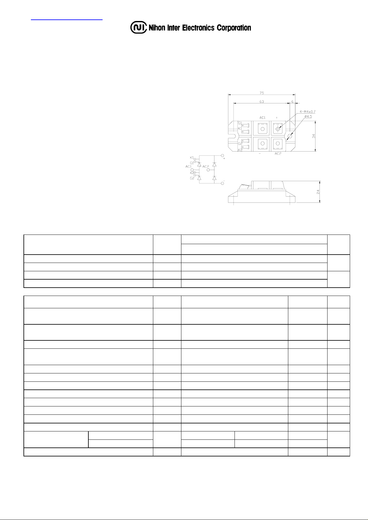
OUTLINE DRAWING
FEATURES
* Isolated Base
* Thyristors and Diodes
H-Bridge Circuit
* High Surge Capability
* UL Recognized, File No. E187184
TYPICAL APPLICATIONS
* Rectified For General Use
Maximum Ratings Approx Net Weight:70g
Parameter
Parameter
ParameterParameter
Repetitive Peak Off-State Voltage
Non Repetitive Peak Off-State Voltage
Repetitive Peak Reverse Voltage
Non Repetitive Peak Reverse Voltage
Parameter
Parameter
Parameter Parameter
Average Rectified Output Current I
Surge On-State Current I
I Squared t I2t 2msec to 10msec 1800 A2s
Critical Rate of Turned-On Current di/dt
Peak Gate Power PGM 5 W
Average Gate Power P
Peak Gate Current IGM 2 A
Peak Gate Voltage VGM 10 V
Peak Gate Reverse Voltage V
Operating JunctionTemperature Range
Storage Temperature Range
Isoration Voltage Viso
Mounting torque
Gate Terminals Treatment Force Ftor Insertion/Pulling out 45/32 N
Value per 1 Arm
Case mounting Greased M4 Screw 0.9 to 1.6
Terminals
Symbol
800
V
DRM
960
V
DSM
V
800
RRM
V
960
RSM
50Hz Half Sine Wave condition
O(AV)
G(AV)
Tjw -40 to +125
Tstg -40 to +125
Ftor
Tc=94°C
50 Hz Half Sine Wave,1Pulse,
TSM
Non-Repetitive
V
=2/3V
D
I
=200mA, diG/dt=0.2A/µs
G
1 W
5 V
RGM
Base Plate to Terminals, AC1min
Conditions
Conditions
ConditionsConditions
, ITM=2•IO, Tj=125°C
DRM
- M4 Screw 1.3 to 1.9
Grade
PBH308AC
Unit
V
V
Max Rated
Max Rated
Max RatedMax Rated
Value
Value
Value Value
30 A
600 A
100
2500 V
Unit
A/µs
°C
°C
N•m
Electrical • Thermal Characteristics
Characteristics
Peak Off-State Current
Peak Reverse Current
Peak Forward Voltage
Symbol Test Conditions
I
DM
I
RM
V
TM
= V
V
DM
V
RM
I
TM
DRM,
= V
RRM,
= 90A, Tj=25°C
Gate Current to Trigger IGT VD=6V,IT=1A
Gate Voltage to Trigger VGT VD=6V,IT=1A
Gate Non-Trigger Voltage VGD
Critical Rate of Rise of Off-State
Voltage
dv/dt
Turn-Off Time t q
=2/3V
V
D
=2/3V
V
D
I
TM=IO,VD
Tj=125°C
DRM
Tj=125°C
DRM
=2/3V
dv/dt=20V/µs, VR=100V
Tj= 125°C
Tj= 125°C
Tj=-40°C
Tj=25°C
Tj=125°C
Tj=-40°C
Tj=25°C
Tj=125°C
DRM
Maximum Value.
Min. Typ. Max.
10 mA
10 mA
1.45 V
200
100
50
4
2.5
2
0.25 V
500
100
-di/dt=20A/µs, Tj = 12 5 °C
Turn-On Time tgt 6
Delay Time t d 2
Rise Time tr
Latching Current IL
Holding Current IH
V
=2/3V
D
I
=200mA, diG/dt=0.2A/µs
G
Tj=125°C
DRM
Tj=25°C
Tj=25°C
4
100 mA
50
Rth(j-c) Junction to Case 0.44
Thermal Resistance *1
Rth(c-f)
Base Plate to Heat Sink
with Thermal Compound
0.1
Value Per 1Arm
*1:Value Per Module
Unit
mA
V
V/µs
µs
µs
µs
µs
°C/W

PBH308AC OUTLINE DRAWING (Dimensions in mm)

 Loading...