

NIHON C10T03QLH-11A Datasheet
SBD Type : C10T03QLH
C10T03QLH----11A
C10T03QLHC10T03QLH
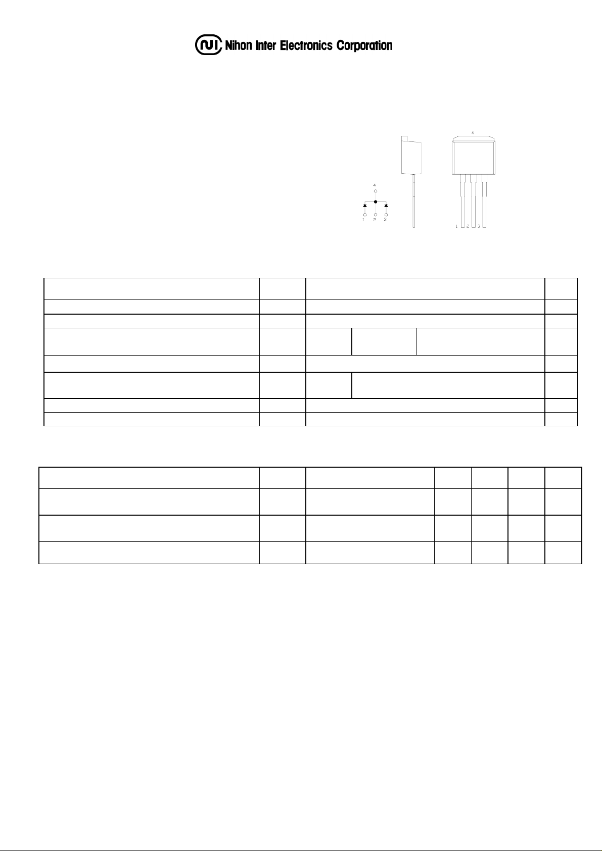
11A OUTLINE DRAWING
11A11A
FEATURES
FEATURES
FEATURESFEATURES
*Tabless TO-220
*Dual Diodes – Cathode Common
*Low Forward Voltage Drop
*High Surge Capability
*Tj=150 °C
operation
Maximum Ratings Approx Net Weight: 1.45g
Rating Symbol
Repetitive Peak Reverse Voltage
Repetitive Peak Surge Reverse Voltage
Average Rectified Output Current IO 10
RMS Forward Current I
Surge Forward Current I
Operating JunctionTemperature Range Tjw -40 to +150
Storage Temperature Range T
V
30
RRM
V
RRSM
F(RMS)
120
FSM
-40 to +150
stg
35(pulse width ≤ 1µs duty ≤ 1/50)
C10T03QLH-11A
Tc=129°C
50Hz Full Sine Wave ,1cycle
Non-repetitive
50 Hz Full Sine Wave
Resistive Load
11.1
Unit
V
V
A
A
A
°C
°C
Electrical • Thermal Characteristics
Characteristics Symbol Conditions Min. Typ. Max. Unit
Peak Reverse Current IRM
Peak Forward Voltage VFM
Thermal Resistance Rth(j -c ) Junction to Case - - 3
Tj= 25°C, V
per arm
Tj= 25°C, I
per arm
= V
RM
= 5 A
FM
RRM
- - 1 mA
- - 0.57 V
°C
/W
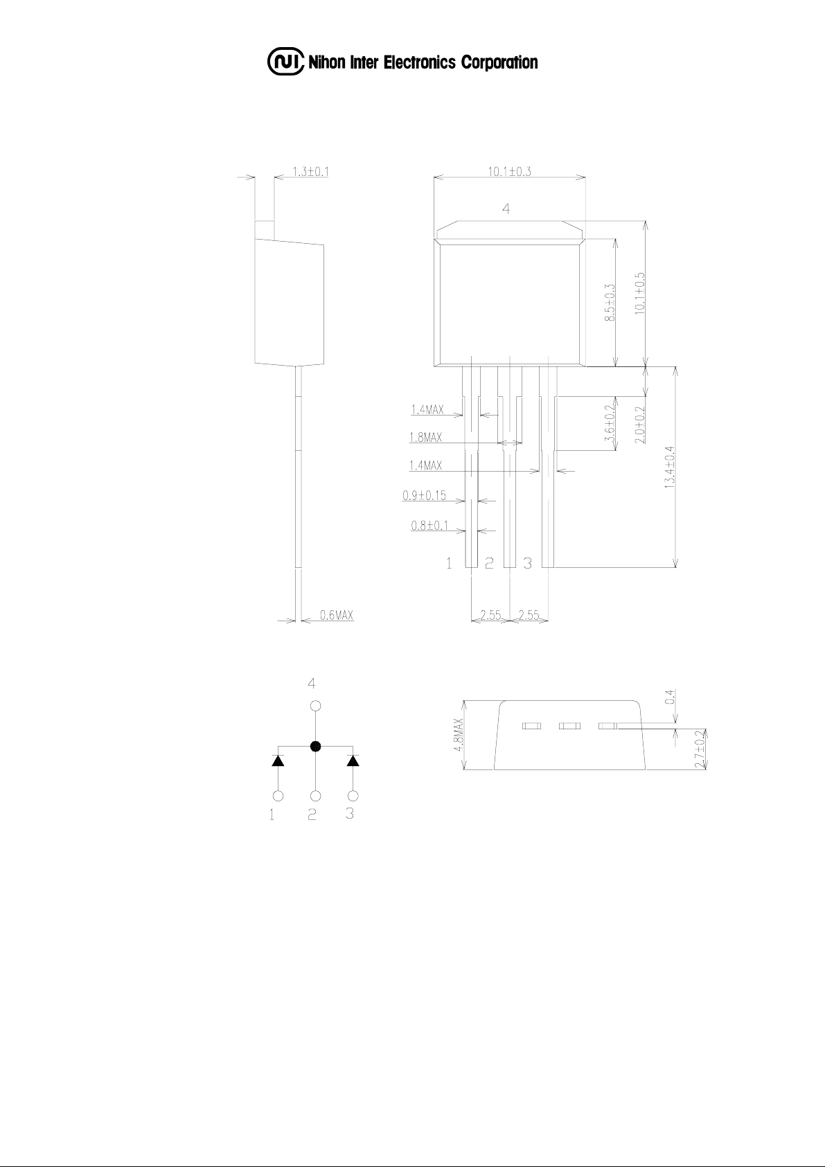
C10T03QLH-11A OUTLINE DRAWING (Dimentions in mm)
 Loading...