


GPIB Hardware Guide
ONFIGURATION AND INSTALLATION
C
AT-GPIB-TNT
GPIB-PCII/IIA
PC/104-GPIB
NEC-GPIB/TNT
NSTALLATION
I
AT-GPIB/TNT (PnP) and AT-GPIB/TNT+
GPIB-1394
GPIB-USB-A
NEC-GPIB/TNT (PnP)
PCI-GPIB and PCI-GPIB+
PCMCIA-GPIB and PCMCIA-GPIB+
PMC-GPIB
PXI-GPIB
PECIFICATIONS
S
ECHNICAL SUPPORT
T
MPORTANT INFORMATION
I
OMPLIANCE
C
322296B-01, March 2000

Configure and Install Your AT-GPIB/TNT
1. Configure the AT-GPIB/TNT Base I/O Address
2. Configure the AT-GPIB/TNT Interrupt Line (IRQ).
3. Configure the AT-GPIB/TNT DMA Channel.
After you finish these steps, you are ready to Install the AT-GPIB/TNT.
Configure and Install Your AT-GPIB/TNT
HOME
Next
Step

1
4 65
2 3
1 Product Name,
Revision Letter, and
Assembly Letter
2 Base I/O Address
3 Serial Number
Figure 1. AT-GPIB/TNT Parts Locator Diagram
Configure and Install Your AT-GPIB/TNT
4 DMA Channel
5 Interrupt Line (IRQ)
6 Shield Ground
Go
Back
HOME

Configure the AT-GPIB/TNT Base I/O Address
Click on the base I/O address assigned to your AT-GPIB/TNT from the list below, and change the
switch settings to match the base I/O address assigned to your board.
If you do not know what resources were assigned to your AT-GPIB/TNT, click here to Determine
Assigned Resources.
100 200 300
120 220 320
140 240 340
160 260 360
180 280 380
1A0 2A0 3A0
1C0 2C0* 3C0
1E0 2E0 3E0
* default setting
Configure and Install Your AT-GPIB/TNT
Previous
Step
HOME
Next
Step

Table 1. Possible Base I/O Address Switch Settings for AT-GPIB/TNT
View Parts
Locator
Diagram
Base I/O
Address (hex)
100 120
140 160
180 1A0
1C0 1E0
Switch Setting
OFF
OFF
OFF
OFF
A9
A8
A7
A6
A5
A9
A8
A7
A6
A5
A9
A8
A7
A6
A5
A9
A8
A7
A6
A5
Base I/O
Address (hex)
Switch Setting
OFF
OFF
OFF
OFF
A9
A8
A7
A6
A5
A9
A8
A7
A6
A5
A9
A8
A7
A6
A5
A9
A8
A7
A6
A5
Configure and Install Your AT-GPIB/TNT
Previous
Step
HOME
Next
Step

Table 1. Possible Base I/O Address Switch Settings for AT-GPIB/TNT (Continued)
View Parts
Locator
Diagram
Base I/O
Address (hex)
200 220
240 260
280 2A0
2C0 2E0
Switch Setting
OFF
OFF
OFF
OFF
A9
A8
A7
A6
A5
A9
A8
A7
A6
A5
A9
A8
A7
A6
A5
A9
A8
A7
A6
A5
Base I/O
Address (hex)
Switch Setting
OFF
OFF
OFF
OFF
A9
A8
A7
A6
A5
A9
A8
A7
A6
A5
A9
A8
A7
A6
A5
A9
A8
A7
A6
A5
Configure and Install Your AT-GPIB/TNT
Previous
Step
HOME
Next
Step

Table 1. Possible Base I/O Address Switch Settings for AT-GPIB/TNT (Continued)
View Parts
Locator
Diagram
Base I/O
Address (hex)
300 320
340 360
380 3A0
3C0 3E0
Switch Setting
OFF
OFF
OFF
OFF
A9
A8
A7
A6
A5
A9
A8
A7
A6
A5
A9
A8
A7
A6
A5
A9
A8
A7
A6
A5
Base I/O
Address (hex)
Switch Setting
OFF
OFF
OFF
OFF
A9
A8
A7
A6
A5
A9
A8
A7
A6
A5
A9
A8
A7
A6
A5
A9
A8
A7
A6
A5
Configure and Install Your AT-GPIB/TNT
Previous
Step
HOME
Next
Step

345679
IRQ3
IRQ9
345679
IRQ3
IRQ9
View Parts
Locator
Diagram
Configure the AT-GPIB/TNT Interrupt Line (IRQ)
Change the jumper settings to match the interrupt line (IRQ) assigned to your board. By default,
the AT-GPIB/TNT is configured to use interrupt line (IRQ) 11.
If you do not know what resources were assigned to your AT-GPIB/TNT, click here to Determine
Assigned Resources.
Table 2. AT-GPIB/TNT Interrupt Line Configurations
Interrupt Line (IRQ) Interrupt Jumper Setting
=
Used to
10, 11, 12, or 15
(IRQ 11 is shown)
3, 4, 5, 7, or 9
(IRQ 5 is shown)
Select
DMA
DRQ7
DACK7
DRQ6
DACK6
DRQ5
DACK5
1514121110
IRQ
No Interrupt Line (IRQ)
Configure and Install Your AT-GPIB/TNT
Previous
Step
HOME
Next
Step

View Parts
Locator
Diagram
Configure the AT-GPIB/TNT DMA Channel
Change the jumper settings to match the DMA channel assigned to your board. You must set both
the DMA Acknowledge and DMA Request lines. By default, the AT-GPIB/TNT is configured to use
DMA channel 5.
If you do not know what resources were assigned to your AT-GPIB/TNT, click here to Determine
Assigned Resources.
Table 3. AT-GPIB/TNT DMA Channel Settings
DMA Channel DMA Jumpers
=
Used to
5, 6, or 7
(DMA 7 is shown)
No DMA Channel
Select
=
Used to
Select
IRQ
IRQ
DRQ7
DACK7
DRQ7
DACK7
DRQ6
DACK6
DRQ6
DACK6
DRQ5
DACK5
DRQ5
DACK5
1514121110
IRQ
1514121110
IRQ
Configure and Install Your AT-GPIB/TNT
Previous
Step
HOME
Next
Step

Set the AT-GPIB/TNT Shield Ground Configuration
The AT-GPIB/TNT is set at the factory with the jumper in place to connect the logic ground of the
AT-GPIB/TNT to its shield ground. This configuration minimizes EMI emissions.
Caution
!
The AT-GPIB/TNT was tested for compliance with FCC standards with the shield ground connected
to logic ground. Removing the jumper might cause EMI emissions to exceed any or all of the
applicable standards.
Most users do not need to change the shield ground configuration. If you feel you must disconnect
logic ground from shield ground, follow these steps:
1. Locate the shield ground jumper W3 on the AT-GPIB/TNT. (View the AT-GPIB/TNT Parts
Locator Diagram.)
2. Remove the jumper and place it across only one of the jumper pins, as shown in the following
figure.
a. Logic Ground Connected to Shield Ground (Default)
b. Logic Ground Disconnected from Shield Ground
Figure 2. AT-GPIB/TNT Ground Configuration Jumper Settings
W3
W3
Configure and Install Your AT-GPIB/TNT
Previous
Step
HOME
Next
Step

Install the AT-GPIB/TNT
PRINT THIS TOPIC!
Your computer needs to be off while you install your AT-GPIB/TNT. To print this topic, select
File»Print, select the Pages radio button, and print pages 11-12.
Caution
!
Electrostatic discharge can damage several components on these GPIB boards. To avoid such
damage in handling your board, touch the antistatic plastic package to a metal part of your
computer chassis before removing the board from the package.
Complete the following steps to install your AT-GPIB/TNT:
1. Make sure that your board is configured to match the assigned resources. (If you are not sure,
view instructions to Configure and Install Your AT-GPIB/TNT.)
2. Shut down Windows and turn off your computer. Keep the computer plugged in so that it
remains grounded while you install the AT-GPIB/TNT.
3. Remove the top cover (or other access panels) to give yourself access to the computer
expansion slots.
4. Find an unused expansion slot in your computer. The AT-GPIB/TNT requires a 16-bit ISA
expansion slot.
5. Remove the corresponding slot cover on the back panel of the computer.
Configure and Install Your AT-GPIB/TNT
Previous
Step
HOME
Next
Step

6. Insert the AT-GPIB/TNT into the slot with the GPIB connector sticking out of the opening on
the back panel, as shown in Figure 3. It might be a tight fit, but do not force the board into
place.
Figure 3. Installing the AT-GPIB/TNT
7. Screw the mounting bracket of the AT-GPIB/TNT to the back panel rail of the computer.
8. Replace the top cover (or the access panel to the expansion slot).
9. Power on your computer and start Windows.
The AT-GPIB/TNT hardware installation is now complete.
Configure and Install Your AT-GPIB/TNT
Previous
Step
HOME
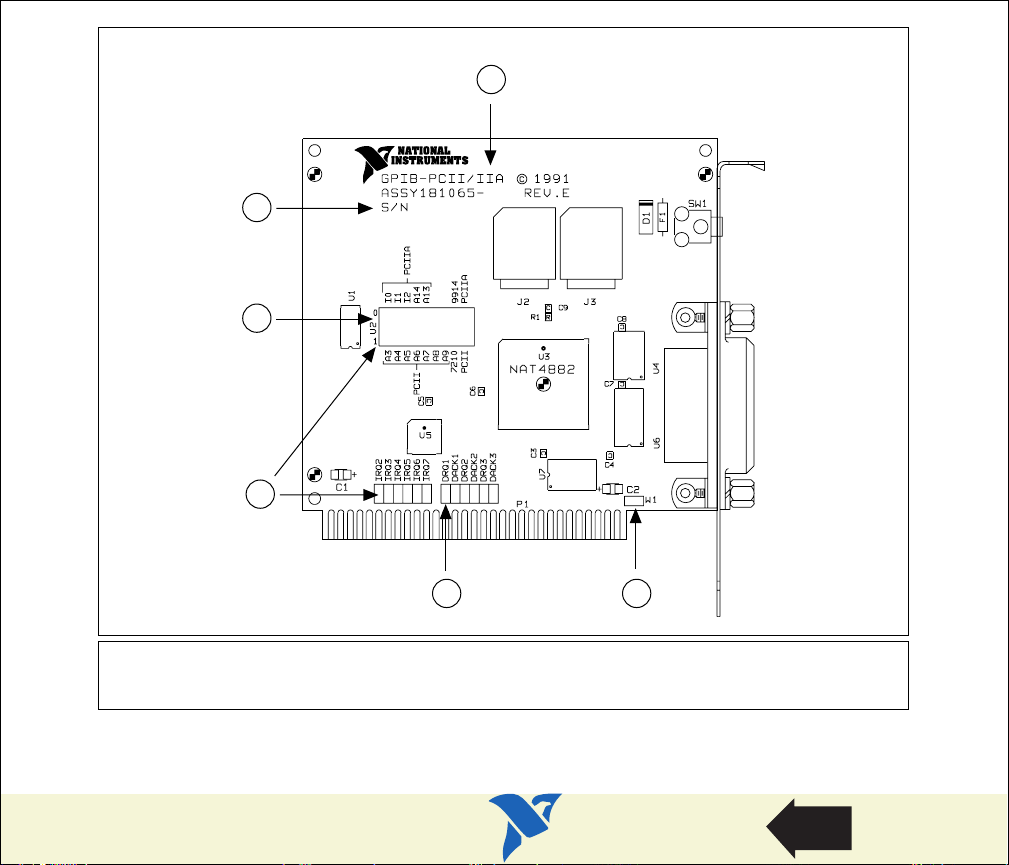
Configure and Install Your GPIB-PCII/IIA
1. Configure the GPIB-PCII/IIA Base I/O Address (GPIB-PCII Mode).
2. Configure the GPIB-PCII/IIA Interrupt Line (IRQ) (GPIB-PCII Mode).
3. Configure the GPIB-PCII/IIA DMA Channel.
After you finish these steps, you are ready to Install the GPIB-PCII/IIA.
National Instruments recommends that you configure the board in PCII mode, using the above
steps. If you want to use your GPIB-PCII/IIA in PCIIA mode, click here to Configure the GPIB-PCII/IIA
in GPIB-PCIIA Mode.
Configure and Install Your GPIB-PCII/IIA
HOME
Next
Step
1
2
3
4
5 6
1 Product Name
2 Assembly
Number, and Revision Number
Number, Serial
3 Base I/O Address
4 Interrupt Line (IRQ)
Figure 4. GPIB-PCII/IIA Parts Locator Diagram
Configure and Install Your GPIB-PCII/IIA
5 DMA Channel
6 Shield Ground
Go
Back
HOME

Configure the GPIB-PCII/IIA Base I/O Address (GPIB-PCII Mode)
Click on the base I/O address assigned to your GPIB-PCII/IIA from the list below, and change the
switch settings to match the base I/O address assigned to your board.
If you do not know what resources were assigned to your GPIB-PCII/IIA, click here to Determine
Assigned Resources.
100 180 200 280 300 380
108 188 208 288 308 388
110 190 210 290 310 390
118 198 218 298 318 398
120 1A0 220 2A0 320 3A0
128 1A8 228 2A8 328 3A8
130 1B0 230 2B0 330 3B0
138 1B8 238 2B8* 338 3B8
140 1C0 240 2C0 340 3C0
148 1C8 248 2C8 348 3C8
150 1D0 250 2D0 350 3D0
158 1D8 258 2D8 358 3D8
160 1E0 260 2E0 360 3E0
168 1E8 268 2E8 368 3E8
170 1F0 270 2F0 370 3F0
178 1F8 278 2F8 378 3F8
*default setting
Configure and Install Your GPIB-PCII/IIA
Previous
Step
HOME
Next
Step

Table 4. Possible Base I/O Address Switch Settings for GPIB-PCII/IIA (PCII Mode)
View Parts
Locator
Diagram
Base I/O
Address (hex)
100 108
110 118
120 128
Switch Setting
U210
1 26897345
OFF
A3
A4
A5
A6
A7
A8
A9
7210 9914
PCII PCIIA
U210
1 26897345
OFF
A3
A4
A5
A6
A7
A8
A9
7210 9914
PCII PCIIA
U210
1 26897345
OFF
A3
A4
A5
A6
A7
A8
A9
7210 9914
PCII PCIIA
Base I/O
Address (hex)
Switch Setting
U210
1 26897345
OFF
A3
A4
A5
A6
A7
A8
A9
7210 9914
PCII PCIIA
U210
1 26897345
OFF
A3
A4
A5
A6
A7
A8
A9
7210 9914
PCII PCIIA
U210
1 26897345
OFF
A3
A4
A5
A6
A7
A8
A9
7210 9914
PCII PCIIA
Configure and Install Your GPIB-PCII/IIA
Previous
Step
HOME
Next
Step

Table 4. Possible Base I/O Address Switch Settings for GPIB-PCII/IIA (PCII Mode) (Continued)
View Parts
Locator
Diagram
Base I/O
Address (hex)
130 138
140 148
150 158
Switch Setting
U210
1 26897345
OFF
A3
A4
A5
A6
A7
A8
A9
7210 9914
PCII PCIIA
U210
1 26897345
OFF
A3
A4
A5
A6
A7
A8
A9
7210 9914
PCII PCIIA
U210
1 26897345
OFF
A3
A4
A5
A6
A7
A8
A9
7210 9914
PCII PCIIA
Base I/O
Address (hex)
Switch Setting
U210
1 26897345
OFF
A3
A4
A5
A6
A7
A8
A9
7210 9914
PCII PCIIA
U210
1 26897345
OFF
A3
A4
A5
A6
A7
A8
A9
7210 9914
PCII PCIIA
U210
1 26897345
OFF
A3
A4
A5
A6
A7
A8
A9
7210 9914
PCII PCIIA
Configure and Install Your GPIB-PCII/IIA
Previous
Step
HOME
Next
Step

Table 4. Possible Base I/O Address Switch Settings for GPIB-PCII/IIA (PCII Mode) (Continued)
View Parts
Locator
Diagram
Base I/O
Address (hex)
160 168
170 178
180 188
Switch Setting
U210
1 26897345
OFF
A3
A4
A5
A6
A7
A8
A9
7210 9914
PCII PCIIA
U210
1 26897345
OFF
A3
A4
A5
A6
A7
A8
A9
7210 9914
PCII PCIIA
U210
1 26897345
OFF
A3
A4
A5
A6
A7
A8
A9
7210 9914
PCII PCIIA
Base I/O
Address (hex)
Switch Setting
U210
1 26897345
OFF
A3
A4
A5
A6
A7
A8
A9
7210 9914
PCII PCIIA
U210
1 26897345
OFF
A3
A4
A5
A6
A7
A8
A9
7210 9914
PCII PCIIA
U210
1 26897345
OFF
A3
A4
A5
A6
A7
A8
A9
7210 9914
PCII PCIIA
Configure and Install Your GPIB-PCII/IIA
Previous
Step
HOME
Next
Step

Table 4. Possible Base I/O Address Switch Settings for GPIB-PCII/IIA (PCII Mode) (Continued)
View Parts
Locator
Diagram
Base I/O
Address (hex)
190 198
1A0 1A8
1B0 1B8
Switch Setting
U210
1 26897345
OFF
A3
A4
A5
A6
A7
A8
A9
7210 9914
PCII PCIIA
U210
1 26897345
OFF
A3
A4
A5
A6
A7
A8
A9
7210 9914
PCII PCIIA
U210
1 26897345
OFF
A3
A4
A5
A6
A7
A8
A9
7210 9914
PCII PCIIA
Base I/O
Address (hex)
Switch Setting
U210
1 26897345
OFF
A3
A4
A5
A6
A7
A8
A9
7210 9914
PCII PCIIA
U210
1 26897345
OFF
A3
A4
A5
A6
A7
A8
A9
7210 9914
PCII PCIIA
U210
1 26897345
OFF
A3
A4
A5
A6
A7
A8
A9
7210 9914
PCII PCIIA
Configure and Install Your GPIB-PCII/IIA
Previous
Step
HOME
Next
Step

Table 4. Possible Base I/O Address Switch Settings for GPIB-PCII/IIA (PCII Mode) (Continued)
View Parts
Locator
Diagram
Base I/O
Address (hex)
1C0 1C8
1D0 1D8
1E0 1E8
Switch Setting
U210
1 26897345
OFF
A3
A4
A5
A6
A7
A8
A9
7210 9914
PCII PCIIA
U210
1 26897345
OFF
A3
A4
A5
A6
A7
A8
A9
7210 9914
PCII PCIIA
U210
1 26897345
OFF
A3
A4
A5
A6
A7
A8
A9
7210 9914
PCII PCIIA
Base I/O
Address (hex)
Switch Setting
U210
1 26897345
OFF
A3
A4
A5
A6
A7
A8
A9
7210 9914
PCII PCIIA
U210
1 26897345
OFF
A3
A4
A5
A6
A7
A8
A9
7210 9914
PCII PCIIA
U210
1 26897345
OFF
A3
A4
A5
A6
A7
A8
A9
7210 9914
PCII PCIIA
Configure and Install Your GPIB-PCII/IIA
Previous
Step
HOME
Next
Step

Table 4. Possible Base I/O Address Switch Settings for GPIB-PCII/IIA (PCII Mode) (Continued)
View Parts
Locator
Diagram
Base I/O
Address (hex)
1F0 1F8
200 208
210 218
Switch Setting
U210
1 26897345
OFF
A3
A4
A5
A6
A7
A8
A9
7210 9914
PCII PCIIA
U210
1 26897345
OFF
A3
A4
A5
A6
A7
A8
A9
7210 9914
PCII PCIIA
U210
1 26897345
OFF
A3
A4
A5
A6
A7
A8
A9
7210 9914
PCII PCIIA
Base I/O
Address (hex)
Switch Setting
U210
1 26897345
OFF
A3
A4
A5
A6
A7
A8
A9
7210 9914
PCII PCIIA
U210
1 26897345
OFF
A3
A4
A5
A6
A7
A8
A9
7210 9914
PCII PCIIA
U210
1 26897345
OFF
A3
A4
A5
A6
A7
A8
A9
7210 9914
PCII PCIIA
Configure and Install Your GPIB-PCII/IIA
Previous
Step
HOME
Next
Step

Table 4. Possible Base I/O Address Switch Settings for GPIB-PCII/IIA (PCII Mode) (Continued)
View Parts
Locator
Diagram
Base I/O
Address (hex)
220 228
230 238
240 248
Switch Setting
U210
1 26897345
OFF
A3
A4
A5
A6
A7
A8
A9
7210 9914
PCII PCIIA
U210
1 26897345
OFF
A3
A4
A5
A6
A7
A8
A9
7210 9914
PCII PCIIA
U210
1 26897345
OFF
A3
A4
A5
A6
A7
A8
A9
7210 9914
PCII PCIIA
Base I/O
Address (hex)
Switch Setting
U210
1 26897345
OFF
A3
A4
A5
A6
A7
A8
A9
7210 9914
PCII PCIIA
U210
1 26897345
OFF
A3
A4
A5
A6
A7
A8
A9
7210 9914
PCII PCIIA
U210
1 26897345
OFF
A3
A4
A5
A6
A7
A8
A9
7210 9914
PCII PCIIA
Configure and Install Your GPIB-PCII/IIA
Previous
Step
HOME
Next
Step

Table 4. Possible Base I/O Address Switch Settings for GPIB-PCII/IIA (PCII Mode) (Continued)
View Parts
Locator
Diagram
Base I/O
Address (hex)
250 258
260 268
270 278
Switch Setting
U210
1 26897345
OFF
A3
A4
A5
A6
A7
A8
A9
7210 9914
PCII PCIIA
U210
1 26897345
OFF
A3
A4
A5
A6
A7
A8
A9
7210 9914
PCII PCIIA
U210
1 26897345
OFF
A3
A4
A5
A6
A7
A8
A9
7210 9914
PCII PCIIA
Base I/O
Address (hex)
Switch Setting
U210
1 26897345
OFF
A3
A4
A5
A6
A7
A8
A9
7210 9914
PCII PCIIA
U210
1 26897345
OFF
A3
A4
A5
A6
A7
A8
A9
7210 9914
PCII PCIIA
U210
1 26897345
OFF
A3
A4
A5
A6
A7
A8
A9
7210 9914
PCII PCIIA
Configure and Install Your GPIB-PCII/IIA
Previous
Step
HOME
Next
Step

Table 4. Possible Base I/O Address Switch Settings for GPIB-PCII/IIA (PCII Mode) (Continued)
View Parts
Locator
Diagram
Base I/O
Address (hex)
280 288
290 298
2A0 2A8
Switch Setting
U210
1 26897345
OFF
A3
A4
A5
A6
A7
A8
A9
7210 9914
PCII PCIIA
U210
1 26897345
OFF
A3
A4
A5
A6
A7
A8
A9
7210 9914
PCII PCIIA
U210
1 26897345
OFF
A3
A4
A5
A6
A7
A8
A9
7210 9914
PCII PCIIA
Base I/O
Address (hex)
Switch Setting
U210
1 26897345
OFF
A3
A4
A5
A6
A7
A8
A9
7210 9914
PCII PCIIA
U210
1 26897345
OFF
A3
A4
A5
A6
A7
A8
A9
7210 9914
PCII PCIIA
U210
1 26897345
OFF
A3
A4
A5
A6
A7
A8
A9
7210 9914
PCII PCIIA
Configure and Install Your GPIB-PCII/IIA
Previous
Step
HOME
Next
Step

Table 4. Possible Base I/O Address Switch Settings for GPIB-PCII/IIA (PCII Mode) (Continued)
View Parts
Locator
Diagram
Base I/O
Address (hex)
2B0 2B8
2C0 2C8
2D0 2D8
Switch Setting
U210
1 26897345
OFF
A3
A4
A5
A6
A7
A8
A9
7210 9914
PCII PCIIA
U210
1 26897345
OFF
A3
A4
A5
A6
A7
A8
A9
7210 9914
PCII PCIIA
U210
1 26897345
OFF
A3
A4
A5
A6
A7
A8
A9
7210 9914
PCII PCIIA
Base I/O
Address (hex)
Switch Setting
U210
1 26897345
OFF
A3
A4
A5
A6
A7
A8
A9
7210 9914
PCII PCIIA
U210
1 26897345
OFF
A3
A4
A5
A6
A7
A8
A9
7210 9914
PCII PCIIA
U210
1 26897345
OFF
A3
A4
A5
A6
A7
A8
A9
7210 9914
PCII PCIIA
Configure and Install Your GPIB-PCII/IIA
Previous
Step
HOME
Next
Step

Table 4. Possible Base I/O Address Switch Settings for GPIB-PCII/IIA (PCII Mode) (Continued)
View Parts
Locator
Diagram
Base I/O
Address (hex)
2E0 2E8
2F0 2F8
300 308
Switch Setting
U210
1 26897345
OFF
A3
A4
A5
A6
A7
A8
A9
7210 9914
PCII PCIIA
U210
1 26897345
OFF
A3
A4
A5
A6
A7
A8
A9
7210 9914
PCII PCIIA
U210
1 26897345
OFF
A3
A4
A5
A6
A7
A8
A9
7210 9914
PCII PCIIA
Base I/O
Address (hex)
Switch Setting
U210
1 26897345
OFF
A3
A4
A5
A6
A7
A8
A9
7210 9914
PCII PCIIA
U210
1 26897345
OFF
A3
A4
A5
A6
A7
A8
A9
7210 9914
PCII PCIIA
U210
1 26897345
OFF
A3
A4
A5
A6
A7
A8
A9
7210 9914
PCII PCIIA
Configure and Install Your GPIB-PCII/IIA
Previous
Step
HOME
Next
Step

Table 4. Possible Base I/O Address Switch Settings for GPIB-PCII/IIA (PCII Mode) (Continued)
View Parts
Locator
Diagram
Base I/O
Address (hex)
310 318
320 328
330 338
Switch Setting
U210
1 26897345
OFF
A3
A4
A5
A6
A7
A8
A9
7210 9914
PCII PCIIA
U210
1 26897345
OFF
A3
A4
A5
A6
A7
A8
A9
7210 9914
PCII PCIIA
U210
1 26897345
OFF
A3
A4
A5
A6
A7
A8
A9
7210 9914
PCII PCIIA
Base I/O
Address (hex)
Switch Setting
U210
1 26897345
OFF
A3
A4
A5
A6
A7
A8
A9
7210 9914
PCII PCIIA
U210
1 26897345
OFF
A3
A4
A5
A6
A7
A8
A9
7210 9914
PCII PCIIA
U210
1 26897345
OFF
A3
A4
A5
A6
A7
A8
A9
7210 9914
PCII PCIIA
Configure and Install Your GPIB-PCII/IIA
Previous
Step
HOME
Next
Step

Table 4. Possible Base I/O Address Switch Settings for GPIB-PCII/IIA (PCII Mode) (Continued)
View Parts
Locator
Diagram
Base I/O
Address (hex)
340 348
350 358
360 368
Switch Setting
U210
1 26897345
OFF
A3
A4
A5
A6
A7
A8
A9
7210 9914
PCII PCIIA
U210
1 26897345
OFF
A3
A4
A5
A6
A7
A8
A9
7210 9914
PCII PCIIA
U210
1 26897345
OFF
A3
A4
A5
A6
A7
A8
A9
7210 9914
PCII PCIIA
Base I/O
Address (hex)
Switch Setting
U210
1 26897345
OFF
A3
A4
A5
A6
A7
A8
A9
7210 9914
PCII PCIIA
U210
1 26897345
OFF
A3
A4
A5
A6
A7
A8
A9
7210 9914
PCII PCIIA
U210
1 26897345
OFF
A3
A4
A5
A6
A7
A8
A9
7210 9914
PCII PCIIA
Configure and Install Your GPIB-PCII/IIA
Previous
Step
HOME
Next
Step

Table 4. Possible Base I/O Address Switch Settings for GPIB-PCII/IIA (PCII Mode) (Continued)
View Parts
Locator
Diagram
Base I/O
Address (hex)
370 378
380 388
390 398
Switch Setting
U210
1 26897345
OFF
A3
A4
A5
A6
A7
A8
A9
7210 9914
PCII PCIIA
U210
1 26897345
OFF
A3
A4
A5
A6
A7
A8
A9
7210 9914
PCII PCIIA
U210
1 26897345
OFF
A3
A4
A5
A6
A7
A8
A9
7210 9914
PCII PCIIA
Base I/O
Address (hex)
Switch Setting
U210
1 26897345
OFF
A3
A4
A5
A6
A7
A8
A9
7210 9914
PCII PCIIA
U210
1 26897345
OFF
A3
A4
A5
A6
A7
A8
A9
7210 9914
PCII PCIIA
U210
1 26897345
OFF
A3
A4
A5
A6
A7
A8
A9
7210 9914
PCII PCIIA
Configure and Install Your GPIB-PCII/IIA
Previous
Step
HOME
Next
Step

Table 4. Possible Base I/O Address Switch Settings for GPIB-PCII/IIA (PCII Mode) (Continued)
View Parts
Locator
Diagram
Base I/O
Address (hex)
3A0 3A8
3B0 3B8
3C0 3C8
Switch Setting
U210
1 26897345
OFF
A3
A4
A5
A6
A7
A8
A9
7210 9914
PCII PCIIA
U210
1 26897345
OFF
A3
A4
A5
A6
A7
A8
A9
7210 9914
PCII PCIIA
U210
1 26897345
OFF
A3
A4
A5
A6
A7
A8
A9
7210 9914
PCII PCIIA
Base I/O
Address (hex)
Switch Setting
U210
1 26897345
OFF
A3
A4
A5
A6
A7
A8
A9
7210 9914
PCII PCIIA
U210
1 26897345
OFF
A3
A4
A5
A6
A7
A8
A9
7210 9914
PCII PCIIA
U210
1 26897345
OFF
A3
A4
A5
A6
A7
A8
A9
7210 9914
PCII PCIIA
Configure and Install Your GPIB-PCII/IIA
Previous
Step
HOME
Next
Step

Table 4. Possible Base I/O Address Switch Settings for GPIB-PCII/IIA (PCII Mode) (Continued)
View Parts
Locator
Diagram
Base I/O
Address (hex)
3D0 3D8
3E0 3E8
3F0 3F8
Switch Setting
U210
1 26897345
OFF
A3
A4
A5
A6
A7
A8
A9
7210 9914
PCII PCIIA
U210
1 26897345
OFF
A3
A4
A5
A6
A7
A8
A9
7210 9914
PCII PCIIA
U210
1 26897345
OFF
A3
A4
A5
A6
A7
A8
A9
7210 9914
PCII PCIIA
Base I/O
Address (hex)
Switch Setting
U210
1 26897345
OFF
A3
A4
A5
A6
A7
A8
A9
7210 9914
PCII PCIIA
U210
1 26897345
OFF
A3
A4
A5
A6
A7
A8
A9
7210 9914
PCII PCIIA
U210
1 26897345
OFF
A3
A4
A5
A6
A7
A8
A9
7210 9914
PCII PCIIA
Configure and Install Your GPIB-PCII/IIA
Previous
Step
HOME
Next
Step

IRQ2
IRQ3
IRQ4
IRQ5
IRQ6
IRQ7
IRQ2
IRQ3
IRQ4
IRQ5
IRQ6
IRQ7
View Parts
Locator
Diagram
Configure the GPIB-PCII/IIA Interrupt Line (IRQ) (GPIB-PCII Mode)
Change the jumper settings to match the interrupt line (IRQ) assigned to your board. By default,
the GPIB-PCII/IIA is configured to use interrupt line (IRQ) 7.
If you do not know what resources were assigned to your GPIB-PCII/IIA, click here to Determine
Assigned Resources.
Table 5. GPIB-PCII Interrupt Line Configurations
Interrupt Line (IRQ) Interrupt Jumper Setting
2, 3, 4, 5, 6, 7
(IRQ 7 is shown)
No Interrupt Line (IRQ)
Configure and Install Your GPIB-PCII/IIA
Previous
Step
HOME
Next
Step

Configure the GPIB-PCII/IIA DMA Channel
DRQ1
DACK1
DRQ2
DACK2
DRQ3
DACK3
DRQ1
DACK1
DRQ2
DACK2
DRQ3
DACK3
Change the jumper settings to match the DMA channel assigned to your board. You must set both
the DMA Acknowledge and DMA Request lines. By default, the GPIB-PCII/IIA is configured to use
DMA channel 1.
If you do not know what resources were assigned to your GPIB-PCII/IIA, click here to Determine
Assigned Resources.
Table 6. GPIB-PCII/IIA DMA Channel Settings
DMA Channel DMA Jumpers
View Parts
Locator
1, 2, or 3
(DMA 3 is shown)
Diagram
No DMA
Configure and Install Your GPIB-PCII/IIA
Previous
Step
HOME
Next
Step

Set the GPIB-PCII/IIA Shield Ground Configuration
The GPIB-PCII/IIA is set at the factory with the jumper in place to connect the logic ground of the
GPIB-PCII/IIA to its shield ground. This configuration minimizes EMI emissions.
Caution
!
The GPIB-PCII/IIA was tested for compliance with FCC and CE standards with the shield ground
connected to logic ground. Removing the jumper might cause EMI emissions to exceed the
applicable standards.
Most users do not need to change the shield ground configuration. If you feel you must disconnect
logic ground from shield ground, follow these steps:
1. Locate the shield ground jumper W1 on the GPIB-PCII/IIA. (View the GPIB-PCII/IIA Parts
Locator Diagram.)
2. Remove the jumper and place it across only one of the jumper pins, as shown in the following
figure.
W1
a. Logic Ground Connected to Shield Ground (Default)
W1
b. Logic Ground Disconnected from Shield Ground
Figure 5. GPIB-PCII/IIA Ground Configuration Jumper Settings
Configure and Install Your GPIB-PCII/IIA
Previous
Step
HOME
Next
Step

Install the GPIB-PCII/IIA
PRINT THIS TOPIC!
Your computer needs to be off while you install your GPIB-PCII/IIA. To print this topic, select
File»Print, select the Pages radio button, and print pages 35-36.
Caution
!
Electrostatic discharge can damage several components on these GPIB boards. To avoid such
damage in handling your board, touch the antistatic plastic package to a metal part of your
computer chassis before removing the board from the package.
Perform the following steps to install the GPIB-PCII/IIA:
1. Make sure that your board is configured to match the assigned resources. (If you are not sure,
view instructions to Configure and Install Your GPIB-PCII/IIA.)
2. Shut down Windows and turn off your computer. Keep the computer plugged in so that it
remains grounded while you install the GPIB-PCII/IIA.
3. Remove the top cover (or other access panels) to give yourself access to the computer
expansion slots.
4. Find an unused expansion slot in your computer.
5. Remove the corresponding slot cover on the back panel of the computer.
Configure and Install Your GPIB-PCII/IIA
Previous
Step
HOME
Next
Step

6. Insert the GPIB-PCII/IIA into the slot with the GPIB connector sticking out of the opening on
the back panel, as shown in Figure 6. It might be a tight fit, but do not force the board
intoplace.
Figure 6. Installing the GPIB-PCII/IIA
7. Screw the mounting bracket of the GPIB-PCII/IIA to the back panel rail of the computer.
8. Replace the top cover (or the access panel to the expansion slot).
9. Turn on your computer and start Windows.
The GPIB-PCII/IIA hardware installation is now complete.
Configure and Install Your GPIB-PCII/IIA
Previous
Step
HOME

Configure the GPIB-PCII/IIA in GPIB-PCIIA Mode
This section describes how to configure your GPIB-PCII/IIA board for use in GPIB-PCIIA mode.
Note
National Instruments recommends that you Configure and Install Your GPIB-PCII/IIA in PCII mode.
The NI-488.2 software allows you to install your GPIB-PCII/IIA board for use in GPIB-PCII or
GPIB-PCIIA mode. The two modes use different I/O addresses and interrupt schemes. However,
you should be aware of a potential problem with the Windows Device Manager when using your
board in GPIB-PCIIA mode under Windows. The Device Manager does not reliably report base
address conflicts involving the GPIB-PCII/IIA in GPIB-PCIIA mode. Additionally, the Device
Manager fails to display all of the I/O addresses used by the GPIB-PCII/IIA in GPIB-PCIIA mode.
Therefore, a base address conflict may go unchecked when using your board in GPIB-PCIIA mode.
Base address conflicts can cause your computer to hang or otherwise behave unreliably.
Therefore, it is safest to use the board only in GPIB-PCII mode, not in GPIB-PCIIA mode.
1. Configure GPIB-PCIIA and 7210 Modes.
2. Configure the GPIB-PCII/IIA Base I/O Address (GPIB-PCIIA Mode).
3. Configure the GPIB-PCII/IIA Interrupt Line (IRQ) (GPIB-PCIIA Mode).
4. Configure the GPIB-PCII/IIA DMA Channel.
After you finish these steps, you are ready to Install the GPIB-PCII/IIA.
Configure and Install Your GPIB-PCII/IIA
Previous
Step
HOME
Next
Step

Configure GPIB-PCIIA and 7210 Modes
The GPIB-PCII/IIA comes already configured to run in PCII and 7210 modes. You need to change
the configuration to PCIIA mode.
1. Examine switch 9 in switch block U2. (Click here to view the GPIB-PCII/IIA Parts Locator
Diagram). Press switch 9 down on the side labeled PCIIA, as shown in the following figure.
U210
12 789345
OFF
6
Figure 7. GPIB-PCIIA Mode Selection Setting
2. Verify that switch 8 is pressed down on the side labeled 7210.
Note
The National Instruments NI-488.2 software requires the board to be in 7210 mode.
Configure and Install Your GPIB-PCII/IIA
7210
PCII
= not used to select the GPIB-PC
or 7210/9914 mode
9914
PCIIA
Previous
Step
HOME
Next
Step

Configure the GPIB-PCII/IIA Base I/O Address (GPIB-PCIIA Mode)
Change the switch settings to match the base I/O address assigned to your board. By default, the
GPIB-PCII/IIA is configured to use base I/O address 2E1 hex when in GPIB-PCIIA mode.
If you do not know what resources were assigned to your GPIB-PCII/IIA, click here to Determine
Assigned Resources.
Table 7. Base I/O Settings for the GPIB-PCII/IIA in PCIIA Mode
Base I/O
Address
View Parts
Locator
2E1 22E1
Diagram
42E1 62E1
Configure and Install Your GPIB-PCII/IIA
Switch Setting
U210
12 789345
OFF
A14
A13
6
PCII PCIIA
U210
12 789345
OFF
A14
A13
6
PCII PCIIA
Base I/O
Address
Switch Setting
U210
12 789345
OFF
6
PCII PCIIA
U210
12 789345
OFF
6
PCII PCIIA
Previous
Step
HOME
A14
A13
A14
A13
Next
Step

Configure the GPIB-PCII/IIA Interrupt Line (IRQ) (GPIB-PCIIA Mode)
Click on the interrupt line (IRQ) setting assigned to your GPIB-PCII/IIA from the list below, and
change the jumper and switch settings to match the interrupt line (IRQ) assigned to your board.
By default, the GPIB-PCII/IIA is configured to use interrupt request line IRQ 7.
If you do not know what resources were assigned to your GPIB-PCII/IIA, click here to Determine
Assigned Resources.
234
567
Interrupt Disabled
Configure and Install Your GPIB-PCII/IIA
Previous
Step
HOME
Next
Step

Table 8. Interrupt Request Settings for GPIB-PCII/IIA in PCIIA Mode
I2
I1
I0
U210
1 26897345
OFF
I2
I1
I0
U210
1 26897345
OFF
View Parts
Locator
Diagram
Interrupt
Line
Switch Jumper
U210
OFF
OFF
U210
1 26897345
1 26897345
I0
I0
I1
I1
I2
I2
IRQ2
IRQ3
IRQ4
IRQ5
IRQ6
IRQ7
Interrupt
Line
Switch Jumper
IRQ2
2 3
OFF
U210
1 26897345
I0
I1
I2
IRQ2
IRQ3
IRQ4
IRQ5
IRQ6
IRQ7
IRQ2
4 5
The remaining steps in the installation and configuration process are the same for GPIB-PCII mode
and GPIB-PCIIA mode. Click here to go to the section Configure the GPIB-PCII/IIA DMA Channel,
and continue configuring and installing your GPIB-PCII/IIA.
IRQ3
IRQ3
IRQ4
IRQ4
IRQ5
IRQ5
IRQ6
IRQ6
IRQ7
IRQ7
Configure and Install Your GPIB-PCII/IIA
Previous
Step
HOME
Next
Step

Table 8. Interrupt Request Settings for GPIB-PCII/IIA in PCIIA Mode (Continued)
I2
I1
I0
U210
1 26897345
OFF
I2
I1
I0
U210
1 26897345
OFF
View Parts
Locator
Diagram
Interrupt
Line
Switch Jumper
OFF
U210
1 26897345
I0
I1
I2
IRQ2
IRQ3
IRQ4
IRQ5
IRQ6
IRQ7
Interrupt
Line
Switch Jumper
IRQ2
6 7
Interrupt
OFF
U210
1 26897345
I0
I1
I2
IRQ2
IRQ3
IRQ4
IRQ5
IRQ6
IRQ7
Disabled
The remaining steps in the installation and configuration process are the same for GPIB-PCII mode
and GPIB-PCIIA mode. Click here to go to the section Configure the GPIB-PCII/IIA DMA Channel,
and continue configuring and installing your GPIB-PCII/IIA.
IRQ3
IRQ4
IRQ5
IRQ6
IRQ7
Configure and Install Your GPIB-PCII/IIA
Previous
Step
HOME
Next
Step

Configure and Install Your PC/104-GPIB
1. Configure the PC/104-GPIB Base I/O Address.
2. Configure the PC/104-GPIB Interrupt Line (IRQ).
3. Configure the PC/104-GPIB DMA Channel.
After you finish these steps, you are ready to Install the PC/104-GPIB.
Configure and Install Your PC/104-GPIB
HOME
Next
Step

12
®
3
6
4
5
1 Product Name and Assembly Number
2 Serial Number
Figure 8. PC/104-GPIB Parts Locator Diagram
Configure and Install Your PC/104-GPIB
3 Base I/O Address
4 DMA Channel
5 Interrupt Line (IRQ)
6 Shield Ground
Go
Back
HOME

Configure the PC/104-GPIB Base I/O Address
Click on the base I/O address assigned to your PC/104-GPIB from the list below, and change the
switch settings to match the base I/O address assigned to your board.
If you do not know what resources were assigned to your PC/104-GPIB, click here to Determine
Assigned Resources.
100 200 300
120 220 320
140 240 340
160 260 360
180 280 380
1A0 2A0 3A0
1C0 2C0* 3C0
1E0 2E0 3E0
*default setting
Configure and Install Your PC/104-GPIB
Previous
Step
HOME
Next
Step

Table 9. Possible Base I/O Address Switch Settings for PC/104-GPIB
View Parts
Locator
Diagram
Base I/O
Address (hex)
100 120
140 160
180 1A0
1C0 1E0
Switch
Settings
OFF
OFF
OFF
OFF
A9
A8
A7
A6
A5
A9
A8
A7
A6
A5
A9
A8
A7
A6
A5
A9
A8
A7
A6
A5
Base I/O
Address (hex)
Switch
Settings
OFF
OFF
OFF
OFF
A9
A8
A7
A6
A5
A9
A8
A7
A6
A5
A9
A8
A7
A6
A5
A9
A8
A7
A6
A5
Configure and Install Your PC/104-GPIB
Previous
Step
HOME
Next
Step

Table 9. Possible Base I/O Address Switch Settings for PC/104-GPIB (Continued)
View Parts
Locator
Diagram
Base I/O
Address (hex)
200 220
240 260
280 2A0
2C0 2E0
Switch
Settings
OFF
OFF
OFF
OFF
A9
A8
A7
A6
A5
A9
A8
A7
A6
A5
A9
A8
A7
A6
A5
A9
A8
A7
A6
A5
Base I/O
Address (hex)
Switch
Settings
OFF
OFF
OFF
OFF
A9
A8
A7
A6
A5
A9
A8
A7
A6
A5
A9
A8
A7
A6
A5
A9
A8
A7
A6
A5
Configure and Install Your PC/104-GPIB
Previous
Step
HOME
Next
Step

Table 9. Possible Base I/O Address Switch Settings for PC/104-GPIB (Continued)
View Parts
Locator
Diagram
Base I/O
Address (hex)
300 320
340 360
380 3A0
3C0 3E0
Switch
Settings
OFF
OFF
OFF
OFF
A9
A8
A7
A6
A5
A9
A8
A7
A6
A5
A9
A8
A7
A6
A5
A9
A8
A7
A6
A5
Base I/O
Address (hex)
Switch
Settings
OFF
OFF
OFF
OFF
A9
A8
A7
A6
A5
A9
A8
A7
A6
A5
A9
A8
A7
A6
A5
A9
A8
A7
A6
A5
Configure and Install Your PC/104-GPIB
Previous
Step
HOME
Next
Step

Configure the PC/104-GPIB Interrupt Line (IRQ)
IRQ 10
IRQ 11
IRQ 12
IRQ 14
IRQ 15
W1
W3
IRQ 9
IRQ 7
IRQ 6
IRQ 5
IRQ 4
IRQ 3
IRQ9
IRQ7
IRQ6
IRQ5
IRQ4
IRQ3
Change the jumper settings to match the interrupt line (IRQ) assigned to your board or, if you are
installing the PC/104-GPIB in an 8-bit stack, to the line in the range IRQ3 to IRQ7 you chose on the
Resources page of the PC/104-GPIB Properties dialog box. By default, the PC/104-GPIB is
configured to use interrupt line IRQ 11.
If you do not know what resources were assigned to your PC/104-GPIB, click here to Determine
Assigned Resources.
Table 10. PC/104-GPIB Interrupt Line Configuration
Interrupt Lines Jumper Setting
View Parts
(IRQ 11 is shown)
Locator
Diagram
Lines 3, 4, 5, 7, or 9
(IRQ 5 is shown)
No IRQ
Lines 10, 11, 12, or 15
Configure and Install Your PC/104-GPIB
Previous
Step
HOME
Next
Step

DRQ7
DRQ5
DACK5
DRQ6
DACK6
DACK7
W2
DRQ7
DRQ5
DACK5
DRQ6
DACK6
DACK7
W2
View Parts
Locator
Diagram
Configure the PC/104-GPIB DMA Channel
If Windows is unable to assign a DMA resource to the PC/104-GPIB, or if you are installing the
PC/104-GPIB in an 8-bit stack, you can configure DMA to none and still use the NI-488.2 software.
Change the jumper settings to match the DMA channel assigned to your board, or to no DMA if
you are installing the PC/104-GPIB in an 8-bit stack. You must set both the DMA Acknowledge and
DMA Request lines. By default, the PC/104-GPIB is configured to use DMA channel 5.
If you do not know what resources were assigned to your PC/104-GPIB, click here to Determine
Assigned Resources.
Table 11. PC/104-GPIB DMA Channel Settings
DMA Channel DMA Jumpers
5, 6, or 7
(DMA 7 is shown)
Configure and Install Your PC/104-GPIB
No DMA
Previous
Step
HOME
Next
Step

Set the PC/104-GPIB Shield Ground Configuration
The PC/104-GPIB is set at the factory with the jumper in place to connect the logic ground of the
PC/104-GPIB to its shield ground. This configuration minimizes EMI emissions.
Note
The PC/104-GPIB was tested for compliance with FCC and CE standards with the shield ground
connected to logic ground. Removing the jumper might cause EMI emissions to exceed any or all
of the applicable standards.
Most users do not need to change the shield ground configuration. If you feel you must disconnect
the logic ground from shield ground, follow these steps:
1. Locate the shield ground jumper W5 on the PC/104-GPIB. (View the PC/104-GPIB Parts Locator
Diagram.)
2. Remove the jumper and place it across only one of the jumper pins, as shown in the following
figure.
W5
a. Logic Ground Connected to Shield Ground (Default)
W5
b. Logic Ground Disconnected from Shield Ground
Figure 9. PC/104-GPIB Ground Configuration Jumper Settings
Configure and Install Your PC/104-GPIB
Previous
Step
HOME
Next
Step

Install the PC/104-GPIB
PRINT THIS TOPIC!
Your computer needs to be off while you install your PC/104-GPIB. To print this topic, select
File»Print, select the Pages radio button, and print pages 52-54.
Caution
!
Electrostatic discharge can damage several components on these GPIB boards. To avoid such
damage in handling your board, touch the antistatic plastic package to a metal part of your
computer chassis before removing the board from the package.
The PC/104-GPIB is available in two versions: stackthrough 16-bit and stackthrough 8-bit. 16-bit
modules have two PC/104 connectors and 8-bit modules have one PC/104 connector. Verify that
you have the correct version for your system.
Complete the following steps to install the PC/104-GPIB. In this section, the term parent module
generically refers to either the parent system or the adjacent PC/104 module you stack the
PC/104-GPIB onto.
1. Shut down Windows and turn off your computer. Keep the computer plugged in so that it
remains grounded while you install the PC/104-GPIB.
2. Mount the provided standoffs to the parent module before installing the PC/104-GPIB. You
might need to install the provided hex nuts on the bottom side of the parent module to secure
the standoffs in place. Notice that the parent module might have only two mounting holes for
the standoffs instead of four; in this case, you need only two standoffs.
3. Plug the PC/104-GPIB into the parent module. The PC/104 header is keyed so that it fits in only
one direction. Do not force the PC/104 connector into place.
After the PC/104-GPIB has been plugged in, ensure proper contact by gently pressing down
at the PC/104 connector region of the PC/104-GPIB until the module is level with respect to
the parent module.
4. Fasten the PC/104-GPIB to the standoffs with the provided 4-40 screws. Refer to the following
figure view how to install the board.
Configure and Install Your PC/104-GPIB
Previous
Step
HOME
Next
Step

1
2
OFF
54321
3
8
5
6
4
7
1 PC/104-GPIB
2 GPIB connection
3 GPIB ribbon cable
4Screw
Figure 10. Installing the PC/104-GPIB
5. Plug the GPIB ribbon cable into the GPIB connection on the PC/104-GPIB. The GPIB connection
is keyed so that it fits in only one direction. Do not force the GPIB ribbon cable connector into
place. The GPIB ribbon cable is 20 in. long and terminated with a panel-mount GPIB connector
that can be mounted for easy access in your system.
Configure and Install Your PC/104-GPIB
5 Standoff
6 Parent module
7 PC/104 connector
8 PC/104 header
Previous
Step
HOME
Next
Step

Note
If you plan to perform HS488 high-speed protocol transfers, you must configure the NI-488.2
software for the amount of GPIB cable length in your system. You must add the 20 in. GPIB ribbon
cable to your total GPIB cable length.
6. Check the installation.
7. Power on your system and start Windows.
Configure and Install Your PC/104-GPIB
Previous
Step
HOME

Configure and Install Your NEC-GPIB/TNT
Configure the NEC-GPIB/TNT Base I/O Address.
After you finish configuration, you are ready to Install the NEC-GPIB/TNT.
Configure and Install Your NEC-GPIB/TNT
HOME
Next
Step

12
3
4
5
1 Product Name and Assembly Number
2 Serial Number
Figure 11. NEC-GPIB/TNT Parts Locator Diagram
Configure and Install Your NEC-GPIB/TNT
3 Base I/O Address
4 Address Decode
5 Shield Ground
Go
Back
HOME

Configure the NEC-GPIB/TNT Base I/O Address
Click on the base I/O address assigned to your NEC-GPIB/TNT from the list below, and change the
switch settings to match the base I/O address assigned to your board.
If you do not know what resources were assigned to your NEC-GPIB/TNT, click here to Determine
Assigned Resources.
1D0 2D0
3D0 4D0
5D0 6D0
7D0*
* default setting
Configure and Install Your NEC-GPIB/TNT
Previous
Step
HOME
Next
Step

Table 12. Possible Base I/O Address Switch Settings for NEC-GPIB/TNT
View Parts
Locator
Diagram
Base I/O
Address
(hex)
Switch Settings
OFF
1
OFF0ON
12345678910
Base I/O
Address
(hex)
W2
1D0 2D0
16 bit
12 bit
1
OFF0ON
12345678910
OFF
W2
3D0 4D0
16 bit
12 bit
Switch Settings
W2
16 bit
12 bit
W2
16 bit
12 bit
OFF0ON
OFF
1
OFF0ON
OFF
1
12345678910
12345678910
Configure and Install Your NEC-GPIB/TNT
Previous
Step
HOME
Next
Step

Table 12. Possible Base I/O Address Switch Settings for NEC-GPIB/TNT (Continued)
View Parts
Locator
Diagram
Base I/O
Address
(hex)
Switch Settings
OFF
W2
1
OFF0ON
12345678910
Base I/O
Address
(hex)
5D0 6D0
16 bit
12 bit
1
OFF0ON
12345678910
OFF
W2
7D0
16 bit
12 bit
Switch Settings
W2
16 bit
12 bit
1
OFF0ON
OFF
12345678910
Configure and Install Your NEC-GPIB/TNT
Previous
Step
HOME
Next
Step

Set the NEC-GPIB/TNT Shield Ground Configuration
The NEC-GPIB/TNT is set at the factory with the jumper in place to connect the logic ground of the
NEC-GPIB/TNT to its shield ground. Thisconfiguration minimizes EMI emissions.
Note
The NEC-GPIB/TNT was tested for compliance with FCC standards with the shield ground
connected to logic ground. Removing the jumper might cause EMI emissions to exceed any or all
of the applicable standards.
Most users do not need to change the shield ground configuration. If you feel you must disconnect
the logic ground from shield ground, follow these steps:
1. Locate the shield ground jumper W1 on the NEC-GPIB/TNT. (View the NEC-GPIB/TNT Parts
Locator Diagram.)
2. Remove the jumper and place it across only one of the jumper pins, as shown in the following
figure.
W1
a. Logic Ground Connected to Shield Ground (Default)
W1
b. Logic Ground Disconnected from Shield Ground
Figure 12. NEC-GPIB/TNT Ground Configuration Jumper Settings
Configure and Install Your NEC-GPIB/TNT
Previous
Step
HOME
Next
Step

Install the NEC-GPIB/TNT
PRINT THIS TOPIC!
Your computer needs to be off while you install your NEC-GPIB/TNT. To print this topic, select
File»Print, select the Pages radio button, and print page 61.
Caution
!
Electrostatic discharge can damage several components on these GPIB boards. To avoid such
damage in handling your board, touch the antistatic plastic package to a metal part of your
computer chassis before removing the board from the package.
Complete the following steps to install the NEC-GPIB/TNT :
1. Make sure that your computer is turned off. Keep the computer plugged in so that it remains
grounded while you install the GPIB hardware.
2. Find an unused expansion slot in your computer.
3. Remove the corresponding slot cover on the back panel of the computer.
4. Insert the NEC-GPIB/TNT into the slot. It might be a tight fit, but do not force the board into
place.
5. Screw the mounting bracket of the NEC-GPIB/TNT to the back panel of the computer.
6. Turn on your computer and start Windows.
The NEC-GPIB/TNT hardware installation is now complete.
Configure and Install Your NEC-GPIB/TNT
Previous
Step
HOME

Determine Assigned Resources
Before you configure and install your board, you need to know the resources assigned to your
hardware.
Windows 98/95:
The Add GPIB Hardware Wizard automatically opens this PDF file after it assigns resources to
your GPIB hardware. The Add GPIB Hardware Wizard window is probably open on your desktop.
Switch to that window to view the resources assigned to your GPIB hardware.
If you do not have the Add GPIB Hardware Wizard running, launch it by selecting
Start»Programs»National Instruments NI-488.2»Add GPIB Hardware. Follow the steps until it
displays the list of resources assigned to your GPIB hardware.
Windows NT:
Windows NT is not a true Plug and Play operating system; therefore, it does not have an Add GPIB
Hardware Wizard concept. When you install new GPIB hardware, try to use the default hardware
settings. If these setting fail due to a resource conflict, use the Start»Programs»Administrative
Tools»Windows NT Diagnostics utility. Use the Resources tab of this utility to get a list of
resources that are known to be in use. This list is not necessarily complete, so remember that the
resources not listed only might be available. The only way to know if a resource is available is to
configure your hardware to use it, try it, and see if the NI-488.2 Troubleshooting Wizard passes.
After you select your resources, configure and install your GPIB hardware using the information in
this PDF file. Then, use the GPIB Configuration Utility to communicate the resources assigned to
your GPIB hardware. Run the NI-488.2 Getting Started Wizard for instructions on using the GPIB
Configuration Utility.
Go
Back
HOME

AT-GPIB/TNT (PnP) and AT-GPIB/TNT+ Installation
PRINT THIS TOPIC!
Your computer needs to be off while you install your interface. To print this topic, select File»Print,
select the Pages radio button, and print pages 63-64.
Caution
!
Electrostatic discharge can damage several components on these GPIB boards. To avoid such
damage in handling your board, touch the antistatic plastic package to a metal part of your
computer chassis before removing the board from the package.
1. Make sure that your computer is turned off. Keep the computer plugged in so that it remains
grounded while you install the GPIB hardware.
2. Remove the top cover (or other access panels) to give yourself access to the computer
expansion slots.
3. Find an unused expansion slot in your computer. The AT-GPIB/TNT (PnP) board requires a
16-bit ISA expansion slot.
4. Remove the corresponding slot cover on the back panel of the computer.
5. Insert the GPIB board into the slot with the GPIB connector sticking out of the opening on the
back panel, as shown in Figure 13. It might be a tight fit, but do not force the board into place.
AT-GPIB/TNT (PnP) and AT-GPIB/TNT+
HOME
Next
Step

Figure 13. Installing the AT-GPIB/TNT (PnP)
6. Screw the mounting bracket of the GPIB board to the back panel rail of the computer.
7. Replace the top cover (or the access panel to the expansion slot), power on your computer,
and start Windows.
The GPIB hardware installation is now complete.
AT-GPIB/TNT (PnP) and AT-GPIB/TNT+
Previous
Step
HOME

GPIB-1394 Installation
1. Screw the DC power connector of the DC power supply into the DC power connector on the
back panel of the GPIB-1394.
2. Plug the DC power supply into an AC outlet. Figure 14 shows how to connect the GPIB-1394.
8
6
5
1 1394 Connector
2 1394 Cable
3. Connect 1394 cable to any available 1394 connector on your PC.
4. Connect 1394 cable to any available 1394 connector on your GPIB-1394.
5. Turn on the GPIB-1394 with the power switch on its front panel. The GPIB-1394 is now
powered by the DC power supply.
The GPIB-1394 installation is now complete.
GPIB-1394 Installation
1
3 DC Power Supply
4 To GPIB Devices
Figure 14. Installing the GPIB-1394
7
2
5 1394 Connectors
6 GPIB-1394
NATIONAL
INSTRUMENTS
3
7 DC Power Connector
8PC
4
HOME

GPIB-USB-A Installation
PRINT THIS TOPIC!
To print this topic, select File»Print, select the Pages radio button, and print page 66.
To install the GPIB-USB-A, connect the USB connector from the GPIB-USB-A to an available USB
port on your computer. The GPIB-USB-A connects directly to most GPIB devices without requiring
a GPIB cable. If your computer is already running, Windows automatically detects the GPIB
hardware. Otherwise, start your computer and Windows will detect the GPIB hardware.
4
3
INSTRUMENTS
NATIONAL
1
2
1 USB Connector
2 To GPIB Devices
GPIB-USB-A Installation
3 GPIB-USB-A
4PC
Figure 15. Installing the GPIB-USB-A
HOME

NEC-GPIB/TNT (PnP) Installation
PRINT THIS TOPIC!
Your computer needs to be off while you install your interface. To print this topic, select File»Print,
select the Pages radio button, and print page 67.
Complete the following steps to install the NEC-GPIB/TNT (PnP):
Caution
!
Electrostatic discharge can damage several components on these GPIB boards. To avoid such
damage in handling your board, touch the antistatic plastic package to a metal part of your
computer chassis before removing the board from the package.
1. Make sure that your computer is turned off. Keep the computer plugged in so that it remains
grounded while you install the GPIB hardware.
2. Find an unused expansion slot in your computer.
3. Remove the corresponding slot cover on the back panel of the computer.
4. Insert the NEC-GPIB/TNT (PnP) into the slot. It might be a tight fit, but do not force the board
into place.
5. Screw the mounting bracket of the NEC-GPIB/TNT (PnP) to the back panel of the computer.
6. Power on your computer and start Windows.
The NEC-GPIB/TNT (PnP) hardware installation is now complete.
NEC-GPIB/TNT (PnP) Installation
HOME

PCI-GPIB and PCI-GPIB+ Installation
PRINT THIS TOPIC!
Your computer needs to be off while you install your interface. To print this topic, select File»Print,
select the Pages radio button, and print pages 68-69.
Caution
!
Electrostatic discharge can damage several components on these GPIB boards. To avoid such
damage in handling your board, touch the antistatic plastic package to a metal part of your
computer chassis before removing the board from the package.
1. Make sure that your computer is turned off. Keep the computer plugged in so that it remains
grounded while you install the GPIB hardware.
2. Remove the top cover (or other access panels) to give yourself access to the computer
expansion slots.
3. Find an unused expansion slot in your computer. The PCI-GPIB requires a PCI slot.
4. Remove the corresponding slot cover on the back panel of the computer.
5. Insert the GPIB board into the slot with the GPIB connector sticking out of the opening on the
back panel, as shown in Figure 16. It might be a tight fit, but do not force the board into place.
PCI-GPIB and PCI-GPIB+ Installation
HOME
Next
Step

PCI Board
PCI Slot
Personal
Computer
Figure 16. Installing the PCI-GPIB
6. Screw the mounting bracket of the GPIB board to the back panel rail of the computer.
7. Replace the top cover (or the access panel to the expansion slot).
8. Power on your computer and start Windows.
The GPIB hardware installation is now complete.
PCI-GPIB and PCI-GPIB+ Installation
Previous
Step
HOME

PCMCIA-GPIB and PCMCIA-GPIB+ Installation
PRINT THIS TOPIC!
To print this topic, select File»Print, select the Pages radio button, and print pages 70-71.
For Windows 98/95:
1. Restart Windows.
2. If the PCMCIA-GPIB is not already inserted, insert it into a free PC Card (PCMCIA) socket. The
card has no jumpers or switches to set, and you do not need to power down the system when
you insert it.
For Windows NT:
1. Power off your computer.
2. Insert the PCMCIA-GPIB into a free PC Card (PCMCIA) socket. The card has no jumpers or
switches to set, and you do not need to power down the system when you insert it.
3. Power on your computer and start Windows.
Figure 17 shows how to insert the PCMCIA-GPIB and how to connect the cable.
PCMCIA-GPIB and PCMCIA-GPIB+
HOME
Next
Step

Figure 17. Inserting the PCMCIA-GPIB
The hardware installation is now complete.
Portable
Computer
PCMCIA
Socket
INSERT CARD
PCMCIA-GPIB
Cable
PCMCIA-GPIB and PCMCIA-GPIB+
Previous
Step
HOME

PMC-GPIB Installation
PRINT THIS TOPIC!
Your computer needs to be off while you install your interface. To print this topic, select File»Print,
select the Pages radio button, and print pages 72-74.
Caution
!
Electrostatic discharge can damage several components on these GPIB boards. To avoid
electrostatic damage when you handle the board, touch the antistatic plastic package to a metal
part of your system chassis before removing the board from the package.
Complete the following steps to install your PMC-GPIB:
1. Turn off your system.
2. Find an unused PMC slot in your system. You may need to remove the host from the system to
access the PMC slot.
3. Remove the corresponding slot filler panel from the host.
4. Insert the PMC-GPIB into the slot as shown in Figure 18. It might be a tight fit, but do not force
the board into place.
PMC-GPIB Installation
HOME
Next
Step

2
3
1
4
1 Host Face Plate
2 PMC-GPIB Board
PMC-GPIB Installation
3 +5 V Voltage Key
4 Mounting Screws
Figure 18. Installing the PMC-GPIB
Previous
Step
HOME
Next
Step

5. Use the mounting hardware provided to fasten the PMC-GPIB to the host.
6. Reinstall the host, if you removed it to install the PMC-GPIB.
7. Turn on your system and start Windows.
The PMC-GPIB hardware installation is now complete.
PMC-GPIB Installation
Previous
Step
HOME

PXI-GPIB Installation
PRINT THIS TOPIC!
Your computer needs to be off while you install your interface. To print this topic, select File»Print,
select the Pages radio button, and print pages 75-77.
Caution
!
Electrostatic discharge can damage several components on these GPIB boards. To avoid
electrostatic damage when you handle the board, touch the antistatic plastic package to a metal
part of your system chassis before removing the board from the package.
Complete the following steps to install your PXI-GPIB:
1. Make sure that your PXI or CompactPCI chassis is turned off. Keep the PXI or CompactPCI
chassis plugged in so that it remains grounded while you install the PXI-GPIB.
2. Choose an unused PXI or CompactPCI 5 V peripheral slot. For maximum performance, the
PXI-GPIB has an onboard DMA controller that can only be used if the board is installed in a slot
that supports bus arbitration, or bus master cards. National Instruments recommends
installing the PXI-GPIB in such a slot. If you install the board in a non-master slot, you must
disable the PXI-GPIB onboard DMA controller using the board-level call
NI-488.2 Online Help for a complete description of
3. Remove the filler panel for the peripheral slot you have chosen.
4. Touch a metal part on your chassis to discharge any static electricity that might be on your
clothes or body.
5. Insert the PXI-GPIB into the selected 5 V slot. Use the injector/ejector handle to fully inject the
device into place. Figure 19 shows how to install the PXI-GPIB into a PXI or CompactPCI
chassis.
ibdma.
ibdma. Refer to the
PXI-GPIB Installation
HOME
Next
Step

3
ON STANDBY
1
2
3
4
5
6
7
2
8
4
1
1 Injector/Ejector Handle (In Down Position)
2 PXI-GPIB Board
PXI-GPIB Installation
3 PXI Chassis
4 Injector/Ejector Rail
Figure 19. Installing the PXI-GPIB
Previous
Step
HOME
Next
Step

6. Screw the front panel of the PXI-GPIB to the front panel mounting rail of the PXI or
CompactPCI chassis.
7. Turn on your PXI or CompactPCI chassis and start Windows.
The PXI-GPIB installation is now complete.
PXI-GPIB Installation
Previous
Step
HOME

Specifications
AT-GPIB/TNT Specifications PCI-GPIB Specifications
AT-GPIB/TNT+ Specifications PCI-GPIB+ Specifications
AT-GPIB/TNT (PnP) Specifications PCMCIA-GPIB Specifications
GPIB-1394 Specifications PCMCIA-GPIB+ Specifications
GPIB-PCII/IIA Specifications PC/104-GPIB Specifications
GPIB-USB-A Specifications PMC-GPIB Specifications
NEC-GPIB/TNT Specifications PXI-GPIB Specifications
NEC-GPIB/TNT (PnP) Specifications
Specifications
HOME

AT-GPIB/TNT Specifications
Characteristic Specification
Dimensions 10.7 cm by 16.5 cm
Table 13. AT-GPIB/TNT Hardware Characteristics
(4.2 in. by 6.5 in.)
AT-GPIB/TNT Specifications
Power Requirement
(from PC AT I/O Channel)
I/O Connector IEEE 488 Standard 24-Pin
Operating Environment
Component Temperature
Relative Humidity
Storage Environment
Temperature
Relative Humidity
EMI FCC Class B Certified
+5 VDC 50 mA Typical
100 mA Maximum
0° to 55° C
10% to 90%, Noncondensing
–20° to 70° C
5% to 90%, Noncondensing
Previous
Step
HOME
Next
Step

Table 14. GPIB Software Transfer Rates for the AT-GPIB/TNT
Transfer Method Maximum GPIB Transfer Rate
3-Wire (IEEE 488) 1.5 Mbytes/s*
High Speed (HS488) 1.6 Mbytes/s*
* Actual speed may vary considerably from speed shown because of system and
instrumentation capabilities.
AT-GPIB/TNT Specifications
Previous
Step
HOME
Next
Step

Declaration of Conformity
according to ISO/IEC Guide 22 and BS 7514
Manufacturer's Name: National Instruments
Manufacturer's Address: 6504 Bridge Point Parkway
The manufacturer hereby declares that the product
Product Name: GPIB Interface Card for ISA
Model Numbers: AT-GPIB/TNT GPIB-HP700-AT
Product Options: All
conforms to the following standards or other normative documents:
Electromagnetic Emissions: EN 55022: 1987
(by Council Directive 89/336/EEC) CISPR 22: 1985 Class B
Electromagnetic Immunity: EN 50082-1: 1992
(by Council Directive 89/336/EEC) IEC 801-2: 1991 4.0 kV by Contact
Safety
: EN 61010-1: 1993
(by Council Directive 73/23/EEC)
Supplementary Information
X2 grade shielded cable is required for electromagnetic compatibility and is available from the manufacturer.
When and Where Issued
11 October 1996
Austin, Texas USA
Austin, Texas 78730-5039
USA
8.0 kV by Air
IEC 801-3: 1991 3.0 V/m
IEC 801-4: 1988 0.5 kV Signal Lines
Eric Lifsey
Compliance Engineer
26 .. 1000 MHz
1.0 kV AC Power Lines
Marks of Compliance European Contact
AT-GPIB/TNT Specifications
National Instruments Corporation (U.K. Ltd.)
21 Kingfisher Court, Hambridge Road
Newbury, Berkshire RG14 5SJ
Tel (44) 1635 523545
Fax (44) 1635 523154
Previous
Step
HOME

AT-GPIB/TNT (PnP) Specifications
Table 15. AT-GPIB/TNT (PnP) Hardware Characteristics
Characteristic Specification
Dimensions 10.7 cm by 16.5 cm
(4.2 in. by 6.5 in.)
AT-GPIB/TNT (PnP) Specifications
Power Requirement
(from PC AT I/O Channel)
I/O Connector IEEE 488 Standard 24-Pin
Operating Environment
Component Temperature
Relative Humidity
Storage Environment
Temperature
Relative Humidity
EMI FCC Class B Certified
+5 VDC 120 mA Typical
240 mA Maximum
0° to 55° C
10% to 90%, Noncondensing
–20° to 70° C
5% to 90%, Noncondensing
Previous
Step
HOME
Next
Step

Table 16. GPIB Software Transfer Rates for the AT-GPIB/TNT (PnP)
Transfer Method Maximum GPIB Transfer Rate
3-Wire (IEEE 488) 1.5 Mbytes/s*
High Speed (HS488) 1.6 Mbytes/s*
* Actual speed may vary considerably from speed shown because of system and
instrumentation capabilities.
AT-GPIB/TNT (PnP) Specifications
Previous
Step
HOME
Next
Step

Declaration of Conformity
according to ISO/IEC Guide 22 and BS 7514
Manufacturer's Name:
Manufacturer's Address: 6504 Bridge Point Parkway
The manufacturer hereby declares that the product
Product Name:
Model Numbers: AT-GPIB/TNT Plug and Play
Product Options: All (Fujitsu and Xylinx)
conforms to the following standards or other normative documents:
Electromagnetic Emissions: EN 55022: 1987
(by Council Directive 89/336/EEC) CISPR 22: 1985 Class B
Electromagnetic Immunity: EN 50082-1: 1992
(by Council Directive 89/336/EEC) IEC 801-2: 1991 4.0 kV by Contact
Safety: EN 61010-1: 1993
(by Council Directive 73/23/EEC)
Supplementary Information
X2 grade shielded cable is required for electromagnetic compatibility and is available from the manufacturer.
When and Where Issued
11 October 1996
Austin, Texas USA
Marks of Compliance European Contact
National Instruments
Austin, Texas 78730-5039
USA
GPIB Interface Card for ISA
8.0 kV by Air
IEC 801-3: 1991 3.0 V/m
IEC 801-4: 1988 0.5 kV Signal Lines
Eric Lifsey
Compliance Engineer
National Instruments Corporation (U.K. Ltd.)
21 Kingfisher Court, Hambridge Road
Newbury, Berkshire RG14 5SJ
Tel (44) 1635 523545
Fax (44) 1635 523154
26 .. 1000 MHz
1.0 kV AC Power Lines
AT-GPIB/TNT (PnP) Specifications
Previous
Step
HOME

AT-GPIB/TNT+ Specifications
Table 17. AT-GPIB/TNT+ Hardware Characteristics
Characteristic Specification
Dimensions 10.67 cm by 16.51 cm
(4.2 in. by 6.5 in.)
AT-GPIB/TNT+ Specifications
Power Requirement
(from PC AT I/O Channel)
I/O Connector IEEE 488 Standard 24-Pin
Operating Environment
Component Temperature
Relative Humidity
Storage Environment
Temperature
Relative Humidity
EMI FCC Class B Certified
+5 VDC 445 mA Typical
845 mA Maximum
0° to 55° C
10% to 90%, Noncondensing
–20° to 70° C
5% to 90%, Noncondensing
Previous
Step
HOME
Next
Step

Table 18. GPIB Software Transfer Rates for the AT-GPIB/TNT+
Transfer Method Maximum GPIB Transfer Rate
3-Wire (IEEE 488) 1.5 Mbytes/s*
High Speed (HS488) 1.6 Mbytes/s*
* Actual speed may vary considerably from speed shown because of system and
instrumentation capabilities.
AT-GPIB/TNT+ Specifications
Previous
Step
HOME
Next
Step

Declaration of Conformity
Manufacturer's Name: National Instruments
Manufacturer's Address: 6504 Bridge Point Parkway
The manufacturer hereby declares that the product
Product Name: GPIB Interface Card for AT
Model Numbers: AT-GPIB/TNT+
Product Options: All
conforms to the following standards or other normative documents:
Electromagnetic Emissions: EN 55022: 1987
(by Council Directive 89/336/EEC) CISPR 22: 1985 Class B
Electromagnetic Immunity: EN 50082-1: 1992
(by Council Directive 89/336/EEC) IEC 801-2: 1991 4.0 kV by Contact
Safety: EN 61010-1: 1993
(by Council Directive 73/23/EEC)
Supplementary Information
X2 grade shielded cable is required for electromagnetic compatibility and is available from the manufacturer.
When and Where Issued
11 October 1996
Austin, Texas USA
Marks of Compliance European Contact
according to ISO/IEC Guide 22 and BS 7514
Austin, Texas 78730-5039
USA
8.0 kV by Air
IEC 801-3: 1991 3.0 V/m
IEC 801-4: 1988 0.5 kV Signal Lines
Eric Lifsey
Compliance Engineer
National Instruments Corporation (U.K. Ltd.)
21 Kingfisher Court, Hambridge Road
Newbury, Berkshire RG14 5SJ
Tel (44) 1635 523545
Fax (44) 1635 523154ire RG14 5SJ
26 .. 1000 MHz
1.0 kV AC Power Lines
AT-GPIB/TNT+ Specifications
Previous
Step
HOME

GPIB-1394 Specifications
Dimensions 14.6 cm by 21.3 cm by 3.8
Power Requirement +9 to 30 VDC 5 W Typical
I/O Connector IEEE 488 Standard 24-Pin
1394 Ports S400, S200, S100 data rates
GPIB Port Compatible with IEEE 488.1 and
Operating Environment
Component Temperature
Relative Humidity
Storage Environment
Temperature
Relative Humidity
Table 19. GPIB-1394 Hardware Characteristics
Characteristic Specification
(5.8 in. by 8.4 in. by 1.5 in.)
at 9 VDC 580 mA Typical
1 A Maximum
Three IEEE 1394 6-pin sockets
IEEE 488.2
0° to 55° C
0% to 90%, Noncondensing
–20° to 70° C
10% to 90%, Noncondensing
GPIB-1394 Specifications
EMI FCC Class A Certified
Previous
Step
HOME
Next
Step

Table 20. GPIB Software Transfer Rate for the GPIB-1394
Transfer Method Maximum GPIB Transfer Rate
3-wire (IEEE 488) >1.4 Mbytes/s*
High Speed (HS488) >4.5 Mbytes/s*
* Actual speed may vary considerably from speed shown because of system and
instrumentation capabilities.
GPIB-1394 Specifications
Previous
Step
HOME
Next
Step

Declaration of Conformity
according to ISO/IEC Guide 22 and BS 7514
Manufacturer's Name: National Instruments
Manufacturer's Address: 11500 North Mopac Expressway
The manufacturer hereby declares that the product
Product Name: GPIB to IEEE-1394 Controller
Model Numbers: GPIB-1394
Product Options: All.
conforms to the following standards or other normative documents:
Electromagnetic Emissions EN 55011: 1991
(by Council Directive 89/336/EEC) CISPR 11: 1990 (mod) Group 1, Class A at 10 meters
Electromagnetic Immunity EN 50082-1: 1992
(by Council Directive 89/336/EEC) IEC 801-2: 1991 (mod) 4.0 kV by Contact
Low Voltage Safety: EN 61010-1: 1993 Based on V-0 rating of printed circuit board material.
(by Council Directive 73/23/EEC)
Supplementary Information
Electromagnetic compatbility (EMC) requires the use of shielded interface cables
When and Where Issued
14 January 1999
Austin, Texas
USA
Marks of Compliance European Contact
Austin, Texas 78759-3504
USA
8.0 kV by Air
IEC 801-3: Draft 5 3.0 V/m
IEC 801-4: 1988 0.5 kV Signal Lines
Authorized Signature
Name: Eric Lifsey
Position: Compliance Engineer
National Instruments Corporation (U.K.) Ltd.
21 Kingfisher Court, Hambridge Road
Newbury, Berkshire RG14 5SJ
Tel (44) 1635 523545
Fax (44) 1635 523154
26 .. 1000 MHz
and 900 MHz Digital RF
1.0 kV AC Power Lines
шшшшшшшшшшшш
GPIB-1394 Specifications
Previous
Step
HOME

GPIB-PCII/IIA Specifications
Characteristic Specification
Dimensions 10.7 cm by 11.1 cm
Table 21. GPIB-PCII/IIA Hardware Characteristics
(4.2 in. by 4.35 in.)
GPIB-PCII/IIA Specifications
Power Requirement
(from PC/XT/AT I/O channel)
I/O Connector IEEE 488 Standard 24-pin
Operating Environment
Component Temperature
Relative Humidity
Storage Environment
Temperature
Relative Humidity
EMI FCC Class B Certified
Table 22. GPIB Software Transfer Rate for the GPIB-PCII/IIA
Transfer Method Maximum GPIB Transfer Rate
3-wire (IEEE 488) 300 kbytes/s*
* Actual speed may vary considerably from speed shown because of system and
instrumentation capabilities.
+5 VDC 50 mA typical
120 mA maximum
0° to 55° C
10% to 90%, noncondensing
–20° to 70° C
5% to 90%, noncondensing
Previous
Step
HOME
Next
Step

Declaration of Conformity
according to ISO/IEC Guide 22 and BS 7514
Manufacturer's Name: National Instruments
Manufacturer's Address:
The manufacturer hereby declares that the product
Product Name: GPIB Interface Card for PC/XT/AT
Model Numbers: GPIB-PCII/IIA/IIB
Product Options:
conforms to the following standards or other normative documents:
Electromagnetic Emissions: EN 55022: 1987
(by Council Directive 89/336/EEC) CISPR 22: 1985 Class B
Electromagnetic Immunity: EN 50082-1: 1992
(by Council Directive 89/336/EEC) IEC 801-2: 1991 4.0 kV by Contact
Safety: EN 60950: 1993
(by Council Directive 73/23/EEC)
Supplementary Information
X2 grade shielded cable is required for electromagnetic compatibility and is available from the manufacturer.
When and Where Issued
11 October 1996
Austin, Texas USA
Marks of Compliance European Contact
6504 Bridge Point Parkway
Austin, Texas 78730-5039
USA
All
8.0 kV by Air
IEC 801-3: 1991 3.0 V/m
IEC 801-4: 1988 0.5 kV Signal Lines
Eric Lifsey
Compliance Engineer
National Instruments Corporation (U.K. Ltd.)
21 Kingfisher Court, Hambridge Road
Newbury, Berkshire RG14 5SJ
Tel (44) 1635 523545
Fax (44) 1635 523154
26 .. 1000 MHz
1.0 kV AC Power Lines
GPIB-PCII/IIA Specifications
Previous
Step
HOME

GPIB-USB-A Specifications
Characteristic Specification
Dimensions 10.7 by 6.5 by 2.7 cm
Table 23. GPIB-USB-A Hardware Characteristics
(3.6 by 2.6 by 1.0 in.)
GPIB-USB-A Specifications
Power Requirement
(from USB host or
self-powered hub)
I/O Connector IEEE 488 Standard 24-pin male
Operating Environment
Temperature
Relative Humidity
Storage Environment
Temperature
Relative Humidity
EMI FCC Class A Verified
Table 24. GPIB Software Transfer Rate for the GPIB-USB-A
Transfer Method Maximum GPIB Transfer Rate
3-wire (IEEE 488) Over 650 kbytes/s*
* Actual speed may vary considerably from speed shown because of system and
instrumentation capabilities.
2 unit loads (200 mA Maximum)
0° to 55° C
10% to 90%, noncondensing
–20° to 70° C
10% to 90%, noncondensing
Previous
Step
HOME
Next
Step

Declaration of Conformity
according to ISO/IEC Guide 22 and BS 7514
Manufacturer's Name: National Instruments
Manufacturer's Address: 11500 North MoPac Expressway
The manufacturer hereby declares that the product
Product Name: GPIB to Universal Serial Bus (USB) Controller
Model Numbers: GPIB-USB-A
Product Options: All
conforms to the following standards or other normative documents:
Council Directive 89/336/EEC, Electromagnetic Compatibility, EN 61326-1:1997 A1:1998 Emission: ISM Group 1, Class A (Referencing
EN 55011:1991 (mod) Distance 10 meters
Immunity: Minimum Requirements (Table 1)
Performance Criteria Continuous Unmonitored Operation
EN 61000-4-2: 1995 4.0 kV by Contact, 8.0 kV by Air
EN 61000-4-3: 1996 3.0 V/m, 80% AM with 1 kHz Sine, 80 .. 1000 MHz. 900 MHz, 200 Hz, Pulsed RF
EN 61000-4-4: 1995 0.5 kV Signal Lines, 1.0 kV AC Power Lines
EN 61000-4-5: 1995 0.5 kV Signal Lines, 0.5 kV Mains DM, 1.0 kV Mains CM
EN 61000-4-6: 1996 3.0 V RMS, 80% AM with 1 kHz Sine, 0.15 .. 80 MHz, AC Mains CM (I/O Waived)
EN 610004-11: 1994 AC Mains, 1 cycle, 100% Interruption
Council Directive 73/23/EEC, Low Voltage Safety, EN 61010-1: 1993
Safety compliance based on material flammability ratings.
Supplementary Information
Electromagnetic compatibility requires the following installation measures:
Good screening (shielding)techniques must be employedthroughout the userinstalled portion ofthe GPIB andUSB systems. All attached
GPIB peripherals must be protective-earth (e.g. three wire mains cords) to control unwanted radiated noise emissions.
1
I/O ports with shielded cables are not tested to EN 61000-4-6 by waiver in EN 61326-1 for shielded I/O lines.
When and Where Issued
18 May 2000
Austin, Texas USA
Austin, Texas 78759-3504 USA
ANSI C63.4)
1
Marks of Compliance European Contact
GPIB-USB-A Specifications
Eric Lifsey
Compliance Engineer
National Instruments Corporation (U.K.) Ltd.
21 Kingfisher Court, Hambridge Road
Newbury, Berkshire RG14 5SJ
Tel (44) 1635 523545
Fax (44) 1635 523154
Previous
Step
HOME

NEC-GPIB/TNT Specifications
Table 25. NEC-GPIB/TNT Hardware Characteristics
Characteristic Specification
Dimensions 17 cm by 14.8 cm
(6.7 in. by 5.8 in.)
NEC-GPIB/TNT Specifications
Power Requirement
(from PC-98 Bus)
I/O Connector IEEE 488 Standard 24-Pin
Operating Environment
Component Temperature
Relative Humidity
Storage Environment
Temperature
Relative Humidity
EMI VCCI Certified
+5 VDC 260 mA Typical
750 mA Maximum
0° to 40° C
10% to 90%, Noncondensing
–20° to 70° C
10% to 90%, Noncondensing
Previous
Step
HOME
Next
Step

Table 26. GPIB Software Transfer Rates for the NEC-GPIB/TNT
Transfer Method Maximum GPIB Transfer Rate
3-Wire (IEEE 488) 1.0 Mbytes/s*
High Speed (HS488) 1.0 Mbytes/s*
* Actual speed may vary considerably from speed shown because of system and
instrumentation capabilities.
NEC-GPIB/TNT Specifications
Previous
Step
HOME

NEC-GPIB/TNT (PnP) Specifications
Table 27. NEC-GPIB/TNT (PnP) Hardware Characteristics
Characteristic Specification
Dimensions 17 cm by 14.8 cm
(6.7 in. by 5.8 in.)
Power Requirement
(from PC-98 Bus)
I/O Connector IEEE 488 Standard 24-Pin
Operating Environment
Component Temperature
Relative Humidity
Storage Environment
Temperature
Relative Humidity
EMI VCCI Certified
+5 VDC 260 mA Typical
750 mA Maximum
0° to 40° C
10% to 90%, Noncondensing
–20° to 70° C
10% to 90%, Noncondensing
NEC-GPIB/TNT (PnP) Specifications
Previous
Step
HOME
Next
Step

Table 28. GPIB Software Transfer Rates for the NEC-GPIB/TNT (PnP)
Transfer Method Maximum GPIB Transfer Rate
3-Wire (IEEE 488) 1.0 Mbytes/s*
High Speed (HS488) 1.0 Mbytes/s*
* Actual speed may vary considerably from speed shown because of system and
instrumentation capabilities.
NEC-GPIB/TNT (PnP) Specifications
Previous
Step
HOME

PCI-GPIB Specifications
Dimensions 13.3 cm by 10.7 cm
Table 29. PCI-GPIB Hardware Characteristics
Characteristic Specification
(5.3 in. by 4.2 in.)
PCI-GPIB Specifications
Power Requirement
(from PCI Bus)
I/O Connector IEEE 488 Standard 24-Pin
Operating Environment
Ambient Temperature
Relative Humidity
Storage Environment
Temperature
Relative Humidity
EMI FCC Class B Certified
+5 VDC 300 mA Typical
450 mA Maximum
0° to 55° C
10% to 90%, Noncondensing
–20° to 70° C
5% to 90%, Noncondensing
Previous
Step
HOME
Next
Step

Table 30. GPIB Software Transfer Rates for the PCI-GPIB
Transfer Method Maximum GPIB Transfer Rate
3-Wire (IEEE 488) 1.5 Mbytes/s*
High Speed (HS488) 7.7 Mbytes/s*
* Actual speed may vary considerably from speed shown because of system and
instrumentation capabilities.
PCI-GPIB Specifications
Previous
Step
HOME
Next
Step
 Loading...