

Page 1

NEXCOM International Co., Ltd.
NEXCOM International Co., Ltd.
Published November 2013
www.nexcom.com
Mobile Computing Solutions
Vehicle Telematics Computer
VTC 7120-BK Series
User Manual
Page 2

Copyright © 2012 NEXCOM International Co., Ltd. All Rights Reserved.
ii
Contents
VTC 7120-BK Series User Manual
Contents
Preface
Copyright .............................................................................................. v
Disclaimer .............................................................................................. v
Acknowledgements ............................................................................... v
Regulatory Compliance Statements ........................................................ v
Declaration of Conformity ....................................................................... v
RoHS Compliance .................................................................................. vi
Warranty and RMA ................................................................................vii
Technical Support and Assistance ............................................................ x
Conventions Used in this Manual ............................................................ x
Global Service Contact Information ........................................................ xi
Package Contents .................................................................................xiii
Chapter 1: Product Introduction
Physical Features .....................................................................................1
VTC 7120-BK ......................................................................................1
Overview ................................................................................................2
Key Features ...........................................................................................2
Hardware Specifications ..........................................................................3
Connector Numbering ............................................................................5
VTC 7120-BK ......................................................................................5
Chapter 2: External Connectors Pinout Description
Power Button ......................................................................................6
Power On & SSD or HD Active LED ......................................................6
WLAN & WWAN Active LED ................................................................7
USB 2.0 Port ........................................................................................7
Reset Button ........................................................................................8
SIM Card Connector-3.5G Wakeup ......................................................8
CFast Card Connector .........................................................................9
Line-out ...............................................................................................9
Mic-in ...............................................................................................10
Mic-in2, Line-out2 .............................................................................10
RS232 Connector ..............................................................................11
LVDS Connector ................................................................................ 11
LAN Connectors ................................................................................12
USB Connector ..................................................................................12
RS422/485 Connector .......................................................................13
VGA Connector .................................................................................13
GPIO Connector ................................................................................14
External 12V (4A) & Car Battery (4A) Power and SMBUS .................... 14
Power Input .......................................................................................15
Chapter 3: Jumpers and Switches
Before You Begin ................................................................................. 16
Precautions ..........................................................................................16
Jumper Settings ....................................................................................17
VTC 7120-BK Jumpers Setting ..............................................................20
CMOS Clear Select ............................................................................20
RS232 – Enable Select .......................................................................20
LVDS Power input Voltage Select .......................................................20
Page 3

Copyright © 2012 NEXCOM International Co., Ltd. All Rights Reserved.
iii
Contents
VTC 7120-BK Series User Manual
CMOS Input Voltage Select ................................................................20
PCI-104 VI/O Voltage Setting .............................................................20
RS232 Connector ..............................................................................21
LVDS Connector+USB0 ...................................................................... 21
GPS I-PEX Connector .........................................................................22
DVI+VGA Connector ........................................................................22
SATA PWR Connector ........................................................................ 23
SATA Connector ................................................................................ 23
Mini-PCIe (WWAN) ............................................................................24
Mini-PCIe (WLAN) ..............................................................................25
PCI-104 Connector ...........................................................................26
MCU Programmer PIN Header ...........................................................27
MCU COM Port .................................................................................27
GAL Programmer PIN Header .............................................................28
Super I/O Temperature Sensor ............................................................ 28
MCU Temperature Sensor .................................................................. 29
LVDS Power Connector ...................................................................... 29
GPS Connector ..................................................................................30
Port80 Connector ..............................................................................30
Bluetooth Connector .........................................................................31
Button Power ....................................................................................31
RTC Battery Connector ...................................................................... 32
Hi-speed Board to Board Connector ..................................................33
High Speed Board-to-Board Connector:
COM Express Row A and Row B ........................................................34
High Speed Board-to-Board Connector:
COM Express Row C and Row D ........................................................37
Chapter 4: Mechanical Dimensions
VTC 7120-BK ....................................................................................40
Chapter 5: System Setup
Removing the Chassis Cover ................................................................41
Installing a GPRS/UMTS/HSDPA Module ...............................................42
Installing a Wireless LAN Module ..........................................................46
Installing a SATA SSD Drive ...................................................................48
Rackmount Brackets .............................................................................50
Chapter 6: Driver Installation.................................51
Appendix A:
Software Demo Utility for I/O Ports of Function Control
Menu Screen .....................................................................................52
1.1 Status ........................................................................................53
1.2 GPIO .........................................................................................53
1.3 WDT Setting ..............................................................................54
1.4 Output Power ............................................................................54
1.5 Power On Delay Time ................................................................ 55
1.6 Power Off Delay Time ................................................................ 55
1.7 3G Module ................................................................................55
1.8 WLAN Module ...........................................................................55
1.9 Wake Up Function .....................................................................56
Appendix B: Using the GPS Feature
u-blox NEO-6Q GPS Module Specification .............................................57
Setup and Using GPS Information .........................................................57
Appendix C: Signal Connection of DI/DO
GPIO Pinout Description ........................................................................61
Digital Input ..........................................................................................61
Digital Output .......................................................................................62
Page 4

Copyright © 2012 NEXCOM International Co., Ltd. All Rights Reserved.
iv
Contents
VTC 7120-BK Series User Manual
Appendix D: OBDII Module Setup and Command
OBDII Module .......................................................................................64
VIOX-CAN01 Setup ...............................................................................64
AT Command Summary ........................................................................65
Simple Data Protocol: (ASCII CODE) ......................................................66
Simple Data Protocol: (HEX CODE) ........................................................67
J1939 Raw Data Protocol (HEX CODE) ..................................................68
J1708 Raw Data Protocol (HEX CODE) ..................................................68
J1939 Packaged Messages Protocol ......................................................69
J1708 Packaged Messages Protocol ......................................................77
J1708 Command Example ....................................................................81
Appendix E: Pin Definition for GPS Dead Reckoning Module
-- VIOB-GPS-DR01
S2532DR Overview ...............................................................................82
Technical Specifications ......................................................................... 82
Page 5

Copyright © 2012 NEXCOM International Co., Ltd. All Rights Reserved.
v
Preface
VTC 7120-BK Series User Manual
Regulatory Compliance Statements
This section provides the FCC compliance statement for Class B devices and
describes how to keep the system CE compliant.
Declaration of Conformity
FCC
This equipment has been tested and verified to comply with the limits for
a Class B digital device, pursuant to Part 15 of FCC Rules. These limits are
designed to provide reasonable protection against harmful interference when
the equipment is operated in a commercial environment. This equipment
generates, uses, and can radiate radio frequency energy and, if not installed
and used in accordance with the instructions, may cause harmful interference
to radio communications. Operation of this equipment in a residential area
(domestic environment) is likely to cause harmful interference, in which
case the user will be required to correct the interference (take adequate
measures) at their own expense.
CE
The product(s) described in this manual complies with all applicable
European Union (CE) directives if it has a CE marking. For computer systems
to remain CE compliant, only CE-compliant parts may be used. Maintaining
CE compliance also requires proper cable and cabling techniques.
Copyright
This publication, including all photographs, illustrations and software, is
protected under international copyright laws, with all rights reserved. No
part of this manual may be reproduced, copied, translated or transmitted
in any form or by any means without the prior written consent from
NEXCOM International Co., Ltd.
Disclaimer
The information in this document is subject to change without prior notice
and does not represent commitment from NEXCOM International Co., Ltd.
However, users may update their knowledge of any product in use by constantly
checking its manual posted on our website: http://www.nexcom.com. NEXCOM
shall not be liable for direct, indirect, special, incidental, or consequential
damages arising out of the use of any product, nor for any infringements
upon the rights of third parties, which may result from such use. Any implied
warranties of merchantability or fitness for any particular purpose is also
disclaimed.
Acknowledgements
VTC 7120-BK and VTC 7120-B2K are trademarks of NEXCOM International
Co., Ltd. All other product names mentioned herein are registered
trademarks of their respective owners.
Preface
Page 6

Copyright © 2012 NEXCOM International Co., Ltd. All Rights Reserved.
vi
Preface
VTC 7120-BK Series User Manual
e13 Mark
The “e” mark is the proof of compliance with directives (laws) required
by the European Union. The Council of European communities in Brussels
issues these directives and all members must accept approved products.
e13 - Luxembourg
For more information, visit http://www.tuv.com/jp/en/_e_mark_and_e_
mark_homologation_for_vehicles_vehicle_components_.html.
RoHS Compliance
NEXCOM RoHS Environmental Policy and Status
Update
NEXCOM is a global citizen for building the digital
infrastructure. We are committed to providing green
products and services, which are compliant with
European Union RoHS (Restriction on Use of Hazardous Substance in
Electronic Equipment) directive 2002/95/EU, to be your trusted green
partner and to protect our environment.
RoHS restricts the use of Lead (Pb) < 0.1% or 1,000ppm, Mercury (Hg)
< 0.1% or 1,000ppm, Cadmium (Cd) < 0.01% or 100ppm, Hexavalent
Chromium (Cr6+) < 0.1% or 1,000ppm, Polybrominated biphenyls (PBB) <
0.1% or 1,000ppm, and Polybrominated diphenyl Ethers (PBDE) < 0.1% or
1,000ppm.
In order to meet the RoHS compliant directives, NEXCOM has established an
engineering and manufacturing task force in to implement the introduction
of green products. The task force will ensure that we follow the standard
NEXCOM development procedure and that all the new RoHS components
and new manufacturing processes maintain the highest industry quality
levels for which NEXCOM are renowned.
How to recognize NEXCOM RoHS Products?
For existing products where there are non-RoHS and RoHS versions, the
suffix “(LF)” will be added to the compliant product name.
All new product models launched after January 2006 will be RoHS compliant.
They will use the usual NEXCOM naming convention.
Page 7

Copyright © 2012 NEXCOM International Co., Ltd. All Rights Reserved.
vii
Preface
VTC 7120-BK Series User Manual
Warranty and RMA
NEXCOM Warranty Period
NEXCOM manufactures products that are new or equivalent to new in
accordance with industry standard. NEXCOM warrants that products will
be free from defect in material and workmanship for 2 years, beginning on
the date of invoice by NEXCOM. HCP series products (Blade Server) which
are manufactured by NEXCOM are covered by a three year warranty period.
NEXCOM Return Merchandise Authorization (RMA)
▪ Customers shall enclose the “NEXCOM RMA Service Form” with the
returned packages.
▪ Customers must collect all the information about the problems
encountered and note anything abnormal or, print out any on-screen
messages, and describe the problems on the “NEXCOM RMA Service
Form” for the RMA number apply process.
▪ Customers can send back the faulty products with or without accessories
(manuals, cable, etc.) and any components from the card, such as CPU
and RAM. If the components were suspected as part of the problems,
please note clearly which components are included. Otherwise, NEXCOM
is not responsible for the devices/parts.
▪ Customers are responsible for the safe packaging of defective products,
making sure it is durable enough to be resistant against further damage
and deterioration during transportation. In case of damages occurred
during transportation, the repair is treated as “Out of Warranty.”
▪ Any products returned by NEXCOM to other locations besides the
customers’ site will bear an extra charge and will be billed to the customer.
Repair Service Charges for Out-of-Warranty Products
NEXCOM will charge for out-of-warranty products in two categories, one is
basic diagnostic fee and another is component (product) fee.
System Level
▪ Component fee: NEXCOM will only charge for main components such as
SMD chip, BGA chip, etc. Passive components will be repaired for free,
ex: resistor, capacitor.
▪ Items will be replaced with NEXCOM products if the original one cannot
be repaired. Ex: motherboard, power supply, etc.
▪ Replace with 3rd party products if needed.
▪ If RMA goods can not be repaired, NEXCOM will return it to the customer
without any charge.
Board Level
▪ Component fee: NEXCOM will only charge for main components, such
as SMD chip, BGA chip, etc. Passive components will be repaired for free,
ex: resistors, capacitors.
▪ If RMA goods can not be repaired, NEXCOM will return it to the customer
without any charge.
Page 8

Copyright © 2012 NEXCOM International Co., Ltd. All Rights Reserved.
viii
Preface
VTC 7120-BK Series User Manual
Warnings
Read and adhere to all warnings, cautions, and notices in this guide and
the documentation supplied with the chassis, power supply, and accessory
modules. If the instructions for the chassis and power supply are inconsistent
with these instructions or the instructions for accessory modules, contact
the supplier to find out how you can ensure that your computer meets
safety and regulatory requirements.
Cautions
Electrostatic discharge (ESD) can damage system components. Do the
described procedures only at an ESD workstation. If no such station is
available, you can provide some ESD protection by wearing an antistatic
wrist strap and attaching it to a metal part of the computer chassis.
Safety Information
Before installing and using the device, note the following precautions:
▪ Read all instructions carefully.
▪ Do not place the unit on an unstable surface, cart, or stand.
▪ Follow all warnings and cautions in this manual.
▪ When replacing parts, ensure that your service technician uses parts
specified by the manufacturer.
▪ Avoid using the system near water, in direct sunlight, or near a heating
device.
▪ The load of the system unit does not solely rely for support from the
rackmounts located on the sides. Firm support from the bottom is highly
necessary in order to provide balance stability.
▪ The computer is provided with a battery-powered real-time clock circuit.
There is a danger of explosion if battery is incorrectly replaced. Replace
only with the same or equivalent type recommended by the manufacturer.
Discard used batteries according to the manufacturer’s instructions.
Installation Recommendations
Ensure you have a stable, clean working environment. Dust and dirt can
get into components and cause a malfunction. Use containers to keep
small components separated.
Adequate lighting and proper tools can prevent you from accidentally
damaging the internal components. Most of the procedures that follow
require only a few simple tools, including the following:
• A Philips screwdriver
• A flat-tipped screwdriver
• A grounding strap
• An anti-static pad
Using your fingers can disconnect most of the connections. It is recommended that you do not use needlenose pliers to disconnect connections
as these can damage the soft metal or plastic parts of the connectors.
Page 9

Copyright © 2012 NEXCOM International Co., Ltd. All Rights Reserved.
ix
Preface
VTC 7120-BK Series User Manual
Safety Precautions
▪ Read these safety instructions carefully.
▪ Keep this User Manual for later reference.
▪ Disconnect this equipment from any AC outlet before cleaning. Use a
damp cloth. Do not use liquid or spray detergents for cleaning.
▪ For plug-in equipment, the power outlet socket must be located near the
equipment and must be easily accessible.
▪ Keep this equipment away from humidity.
▪ Put this equipment on a stable surface during installation. Dropping it or
letting it fall may cause damage.
▪ Do not leave this equipment in either an unconditioned environment or
in a above 40
o
C storage temperature as this may damage the equipment.
▪ The openings on the enclosure are for air convection to protect the
equipment from overheating. DO NOT COVER THE OPENINGS.
▪ Make sure the voltage of the power source is correct before connecting
the equipment to the power outlet.
▪ Place the power cord in a way so that people will not step on it. Do not
place anything on top of the power cord. Use a power cord that has been
approved for use with the product and that it matches the voltage and
current marked on the product’s electrical range label. The voltage and
current rating of the cord must be greater than the voltage and current
rating marked on the product.
▪ All cautions and warnings on the equipment should be noted.
▪ If the equipment is not used for a long time, disconnect it from the power
source to avoid damage by transient overvoltage.
▪ Never pour any liquid into an opening. This may cause fire or electrical
shock.
▪ Never open the equipment. For safety reasons, the equipment should be
opened only by qualified service personnel.
▪ If one of the following situations arises, get the equipment checked by
service personnel:
a. The power cord or plug is damaged.
b. Liquid has penetrated into the equipment.
c. The equipment has been exposed to moisture.
d. The equipment does not work well, or you cannot get it to work
according to the user’s manual.
e. The equipment has been dropped and damaged.
f. The equipment has obvious signs of breakage.
▪ Do not place heavy objects on the equipment.
▪ The unit uses a three-wire ground cable which is equipped with a third
pin to ground the unit and prevent electric shock. Do not defeat the
purpose of this pin. If your outlet does not support this kind of plug,
contact your electrician to replace your obsolete outlet.
▪ CAUTION: DANGER OF EXPLOSION IF BATTERY IS INCORRECTLY
REPLACED. REPLACE ONLY WITH THE SAME OR EQUIVALENT TYPE
RECOMMENDED BY THE MANUFACTURER. DISCARD USED BATTERIES
ACCORDING TO THE MANUFACTURER’S INSTRUCTIONS.
▪ The computer is provided with CD drives that comply with the appropriate
safety standards including IEC 60825.
Page 10

Copyright © 2012 NEXCOM International Co., Ltd. All Rights Reserved.
x
Preface
VTC 7120-BK Series User Manual
Conventions Used in this Manual
Warning:
Information about certain situations, which if not observed,
can cause personal injury. This will prevent injury to yourself
when performing a task.
CAUTION!
CAUTION!CAUTION!
Caution:
Information to avoid damaging components or losing data.
Note:
Provides additional information to complete a task easily.
Technical Support and Assistance
1. For the most updated information of NEXCOM products, visit NEXCOM’s
website at www.nexcom.com.
2. For technical issues that require contacting our technical support team or
sales representative, please have the following information ready before
calling:
– Product name and serial number
– Detailed information of the peripheral devices
– Detailed information of the installed software (operating system,
version, application software, etc.)
– A complete description of the problem
– The exact wordings of the error messages
Warning!
1. Handling the unit: carry the unit with both hands and handle it with care.
2. Maintenance: to keep the unit clean, use only approved cleaning products
or clean with a dry cloth.
3. CompactFlash: Turn off the unit’s power before inserting or removing a
CompactFlash storage card.
Page 11

Copyright © 2012 NEXCOM International Co., Ltd. All Rights Reserved.
xi
Preface
VTC 7120-BK Series User Manual
Global Service Contact Information
Headquarters
NEXCOM International Co., Ltd.
15F, No. 920, Chung-Cheng Rd.,
ZhongHe District, New Taipei City, 23586,
Taiwan, R.O.C.
Tel: +886-2-8226-7786
Fax: +886-2-8226-7782
www.nexcom.com
America
USA
NEXCOM USA
2883 Bayview Drive,Fremont CA 94538,
USA
Tel: +1-510-656-2248
Fax: +1-510-656-2158
Email: [email protected]
www.nexcom.com
Asia
Taiwan
Central Taiwan Office
16F, No.250, Sec. 2, Chongde Rd.,
Beitun Dist., Taichung City 406, R.O.C.
Tel: +886-4-2249-1179
Fax: +886-4-2249-1172
Email: [email protected]
www.nexcom.com.tw
Japan
NEXCOM Japan
9F, Tamachi Hara Bldg.,4-11-5, Shiba Minato-ku,
Tokyo, 108-0014, Japan
Tel: +81-3-5419-7830
Fax: +81-3-5419-7832
Email: [email protected]
www.nexcom-jp.com
China
NEXCOM China
2F, Block 4, Venus Plaza, Bldg. 21,
ZhongGuanCun Software Park, No. 8,
Dongbeiwang West Rd., Haidian District,
Beijing, 100193, China
Tel: +86-10-8282-5880
Fax: +86-10-8282-5955
Email: [email protected]
www.nexcom.cn
Shanghai Office
Room 1505, Greenland He Chuang Bldg.,
No. 450 Caoyang Rd.,
Shanghai, 200062, China
Tel: +86-21-6150-8008
Fax: +86-21-3251-6358
Email: [email protected]
www.nexcom.cn
Nanjing Office
Hall C, Block 17, Tian Xing Cui Lang Bldg.,
No. 49 Yunnan North Rd.,
Nanjing, 210018, China
Tel: +86-25-8315-3486
Fax: +86-25-8315-3489
Email: [email protected]
www.nexcom.cn
Shenzhen Office
Western Room 708, Block 210,
Tairan Industry & Trading Place,
Futian Area, Shenzhen,
518040, China
Tel: +86-755-8332-7203
Fax: +86-755-8332-7213
Email: [email protected]
www.nexcom.cn
Wuhan Office
1-C1804/ 1805, Mingze Liwan,
No. 519 South Luoshi Rd.,
Hongshan District,
Wuhan, 430070, China
Tel: +86-27-8722-7400
Fax: +86-27-8722-7400
Email: [email protected]
www.nexcom.cn
Page 12

Copyright © 2012 NEXCOM International Co., Ltd. All Rights Reserved.
xii
Preface
VTC 7120-BK Series User Manual
Chengdu Office
9F, Shuxiangxie, Xuefu Garden,
No.12 Section 1, South Yihuan Rd.,
Chengdu, 610061, China
Tel: +86-28-8523-0186
Fax: +86-28-8523-0186
Email: [email protected]
www.nexcom.cn
Europe
France
NEXCOM France
La Grande Arche-Paroi Nord,
92044 Paris La Défense, France
Tel: +33 (0) 1 40 90 33 35
Fax: +33 (0) 1 40 90 31 01
Email: [email protected]
www.nexcom.eu
Germany
NEXCOM GmbH
Leopoldstraße Business Centre,
Leopoldstraße 244,
80807 Munich, Germany
Tel: +49-89-208039-278
Fax: +49-89-208039-279
Email: [email protected]
www.nexcom.eu
Italy
NEXCOM ITALIA S.r.l
Via Gaudenzio Ferrari 29,
21047 Saronno (VA), Italia
Tel: +39 02 9628 0333
Fax: +39 02 9286 9215
Email: [email protected]
www.nexcomitalia.it
United Kingdom
NEXCOM EUROPE
10 Vincent Avenue,
Crownhill Business Centre,
Milton Keynes, Buckinghamshire MK8 0AB,
United Kingdom
Tel: +44-1908-267121
Fax: +44-1908-262042
Email: [email protected]
www.nexcom.eu
Page 13
Copyright © 2012 NEXCOM International Co., Ltd. All Rights Reserved.
xiii
Preface
VTC 7120-BK Series User Manual
Package Contents
Before continuing, verify that the VTC 7120-BK series package that you received is complete. Your VTC 7120-BK series package should have all the items listed
in the following table.
Item P/N Name Specification Qty
1 50311F0110X00 (H)Flat Head Screw Long FEI:F3x5ISO+NYLOK NIGP F3x5 NI NYLOK 4
2 60233PW134X00 Power Cable For VTK33B SMBus Signal
EDI:356206060201-RS
ATX POWER CON. 6P TO 6P PITCH:4.2mm L:200mm 1
3 60233SAM05X00 GPS Antenna ARKNAV:A-130 GPS Antenna 5M
SMA180P R1 L3
FOR VTC 5M/SMA180P 1
4 602DCD0527X00 Driver CD 1
5 4NCPM00302X00 (T)Terminal Blocks 3P Phoenix Contact:1777992 5.08mm MALE DIP GREEN 1
Page 14

Copyright © 2012 NEXCOM International Co., Ltd. All Rights Reserved.
xiv
Preface
VTC 7120-BK Series User Manual
Ordering Information
The following provides ordering information for VTC 7120-BK series.
• VTC 7120-BK (P/N: 10V00712000X0)
Intel
®
Celeron® 847E 1.1GHz, 2GB DDR3 SODIMM, LVDS/ VGA
Output, 1x RS-232, 1x RS-422/485
Page 15
Copyright © 2012 NEXCOM International Co., Ltd. All Rights Reserved.
1
Chapter 1: Product Introduction
VTC 7120-BK Series User Manual
Chapter 1: Product Introduction
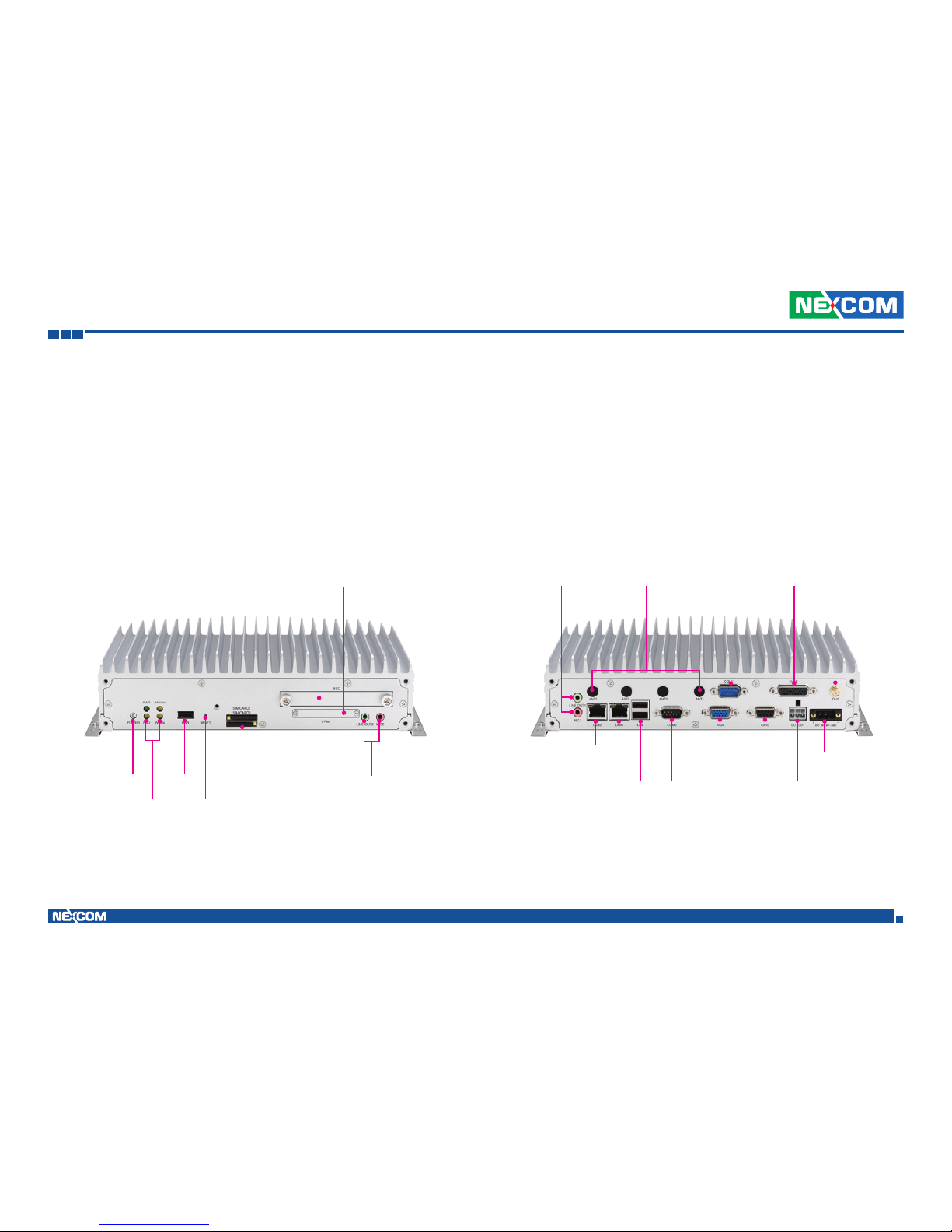
Physical Features
VTC 7120-BK
Power button USB
Reset button
SIM card sockets
Line-out2
Mic-in2
SSD1 CFast
LED indicators
Line-out1
Mic-in1
USB
COM2 VGA
GPIO
DC input
9V~36V
DC output
LAN1
LAN2
Antenna holes COM1 LVDS GPS connector
Page 16

Copyright © 2012 NEXCOM International Co., Ltd. All Rights Reserved.
2
Chapter 1: Product Introduction
VTC 7120-BK Series User Manual
Overview
VTC 7120-BK series, adopting the Intel® high performance processor, is
a new generation of VTC series. In addition to keeping the advantage of
existing VTC series, it offers dual LAN ports for redundancy, two high speed
interface for storage, 2.5” SATA and CFast. The storage is easily accessible
from the front side for maintenance concern. Furthermore, it offers OBDII
for heavy duty truck such as SAE J1939/ J1708.
VTC 7120-BK series fulfills vehicle industry requirements. The design itself
is compliant with vehicle industrial standard such as eMark. More features
required for in-vehicle operations, such as power ignition delay control,
low-power protection and SMBus connection, etc., are continued from
NEXCOM’s other in-vehicle computer products. The GPS function navigates
drivers to ultimate fleet management. Optional 802.11b/g/n, 3.5G, GPRS,
and Bluetooth availability make VTC 7120-BK series ready for wider coverage
and future trend. Multiple display connections make VTC 7120-BK series an
ideal choice for in-vehicle signage platforms as well.
Key Features
• Built-in Intel® processor
• Support two Ethernet LAN ports
• Removal 1x 2.5" SSD tray
• Optional OBDII supporting SAE J1939 or J1708
• 9~36V wide range DC power input
• Smarter ignition power on/off, delay-time and low voltage protection
• Rugged fanless design to meet MIL standard
Page 17

Copyright © 2012 NEXCOM International Co., Ltd. All Rights Reserved.
3
Chapter 1: Product Introduction
VTC 7120-BK Series User Manual
Hardware Specifications
CPU
▪ Intel® Celeron® 847E 1.1GHz
Main Chipset
▪ QM67
Memory
▪ One 204-pin SO-DIMM DDR3 1333 up to 8GB. 2GB (default)
Expansion
▪ 1x Mini-PCIe socket (PCIe + USB) for WLAN option
▪ 1x Mini-PCIe socket (USB) for WWAN option
▪ 1x Bluetooth module for option
▪ 1x on board uBlox NEO-6Q GPS module or optional GPS module with dead
reckoning
I/O Interface-Front
▪ 1x Line-out, 1x Mic-in (for WWAN CM8000 voice communication)
▪ 2x SIM card socket (selectable)
▪ 1x System reset button
▪ 1x USB 2.0 host type A connector
▪ 1x Power button
▪ 1x CFast with protection cover
▪ 1x Accessible 2.5” SATA II SSD tray
▪ 4x LED’s for power, storage, WLAN/ WWAN and GPIO
I/O Interface-Rear
▪ 1x 9~36VDC input with Ignition
▪ 1x 12V/4A DC output, SMBus
▪ 1x DB26 LVDS interface with 12V and USB2.0
▪ 1x DB15 VGA
▪ 1x DB9 RS-232 (default) or OBDII (optional)
▪ 1x DB9 RS-422/ 485
▪ 1x DB9 female connector for 4x DI and 4x DO
(Digital Input)
Input Voltage (Internal Type): 5VDC TTL (default)
Input Voltage (Source Type): 0~30 VDC
(Digital Output)
Digital Output (Sink Type): 5VDC TTL (default), max current: 20mA
Digital Output (Source Type): 0~30VDC, max current: 250mA
▪ 2x USB 2.0 host type A connector
▪ 2x RJ45 with LEDs for 10/ 100/ 1000Mbps Ethernet
▪ 1x Line-out, 1x Mic-in
▪ 1x SMA-type GPS antenna connector
▪ 4x Antenna hole reserved for SMA-type antenna connector (WWAN/
WLAN/ BT)
Others
▪ 1x PCI-104
▪ 1x G Sensor
Note: If PCI-104 installation is needed, please contact NEXCOM for further information.
Power Management
▪ Selectable boot-up & shut-down voltage for low power protection by
software
▪ Setting 8-level on/off delay time by software
▪ Status of ignition and low voltage status can be detected by software
▪ Support S3/ S4 suspend mode
Dimensions
▪ 260mm (W) x 176mm (D) x 66.5mm (H) (10.24”x 6.93”x 2.59”)
▪ 3.25 Kg (7.16 Lb)
Construction
▪ Aluminum enclosure with fanless design
Page 18

Copyright © 2012 NEXCOM International Co., Ltd. All Rights Reserved.
4
Chapter 1: Product Introduction
VTC 7120-BK Series User Manual
Environment
▪ Operating temperatures:
Ambient with air: -30°C to 50°C
▪ Storage temperatures: -35°C to 85°C
▪ Relative humidity: 10% to 90% (non-condensing)
▪ Vibration (random): 1g@5~500 Hz (in operation, SSD)
▪ Vibration (SSD):
Operating: MIL-STD-810G, Method 514.6, Category 4, common
carrier US highway truck vibration exposure
Storage: MIL-STD-810G, Method 514.6, Category 24, minimum integrity test
▪ Shock (SSD):
Operating: MIL-STD-810G, Method 516.6, Procedure I, functional shock=20g
Non-Operating: MIL-STD-810G, Method 516.6, Procedure V, crash hazard
shock test=75g
Operating System
▪ Tizen IVI
Certifications
▪ CE approval
▪ FCC Class A
▪ e13 Mark
Power Management
▪ Power-on delay time is selectable by BIOS to disable and enable in 10sec /
30sec / 1min / 5min / 10 min / 15min / 30min / 1hr.
▪ Power-off delay time is selectable by BIOS to disable and enable in 20sec /
1min / 5min / 10min / 30min / 1hr / 6hr / 18hr.
▪ S3, S4 suspend mode
▪ Ignition On/Off status detectable by SW
▪ Low battery status detectable by SW
▪ Ignition enable/disable is jumper selectable
▪ Shut down system automatically when the system’s internal temperature
is over 80C.
▪ VTC 71 series will automatically shut down 5 minutes after the duration
of low battery voltage is over 60 sec. User can detect this situation via
software.
▪ If the ignition is off and the system is still on after 3 minutes, VTC 71
series will shut down automatically.
▪ If the ignition is off, the user can detect this status via the software.
▪ If the ignition is turned on again and the power-off delay is in progress,
VTC 71 series will cancel the delay function and will continue to operate
normally.
▪ If the ignition is turned on again and the power-off delay ended,
VTC 71 series will shut down completely will power-on again
automatically.
▪ If the ignition is turned off again and power-on delay is in progress,
VTC 71 series will cancel the delay and stay in power-off status.
▪ If the ignition is turned off again and the power-on delay ended (entered
OS already), VTC 71 series will continue to operate normally.
▪ If the ignition is turned off again and the power-on delay ended (in BIOS
process), VTC 71 series will shut down immediately.
▪ If VTC 71 series is off, only below 10mA is used.
Page 19
Copyright © 2012 NEXCOM International Co., Ltd. All Rights Reserved.
5
Chapter 1: Product Introduction
VTC 7120-BK Series User Manual
Connector Numbering
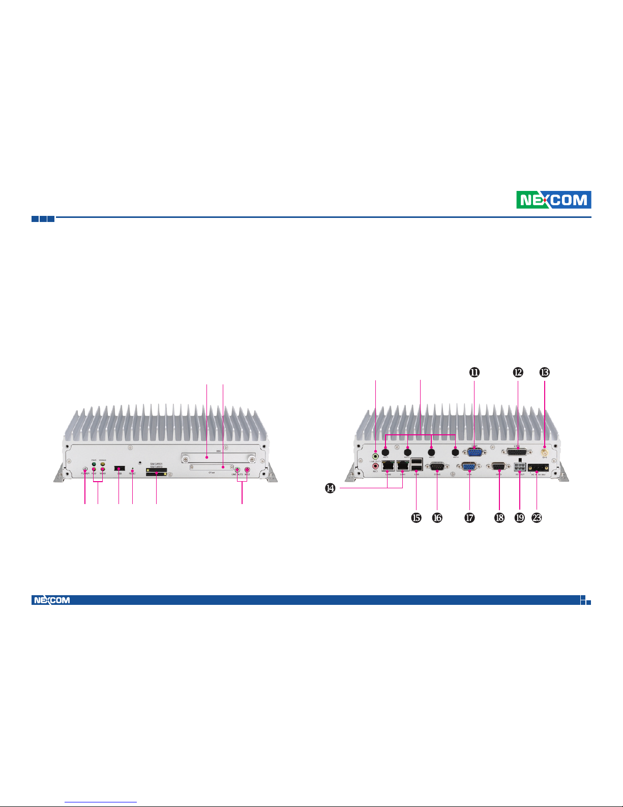
The following diagrams indicate the numbers of the connectors. Use these
numbers to locate the connectors’ respective pinout assignments on chapter 2
of the manual. Please note that connector numbers 6, 10, and 13 pinouts are
not available.
VTC 7120-BK
Page 20
Copyright © 2012 NEXCOM International Co., Ltd. All Rights Reserved.
6
Chapter 2: External Connectors Pinout Description
VTC 7120-BK Series User Manual
Chapter 2: External Connectors Pinout Description
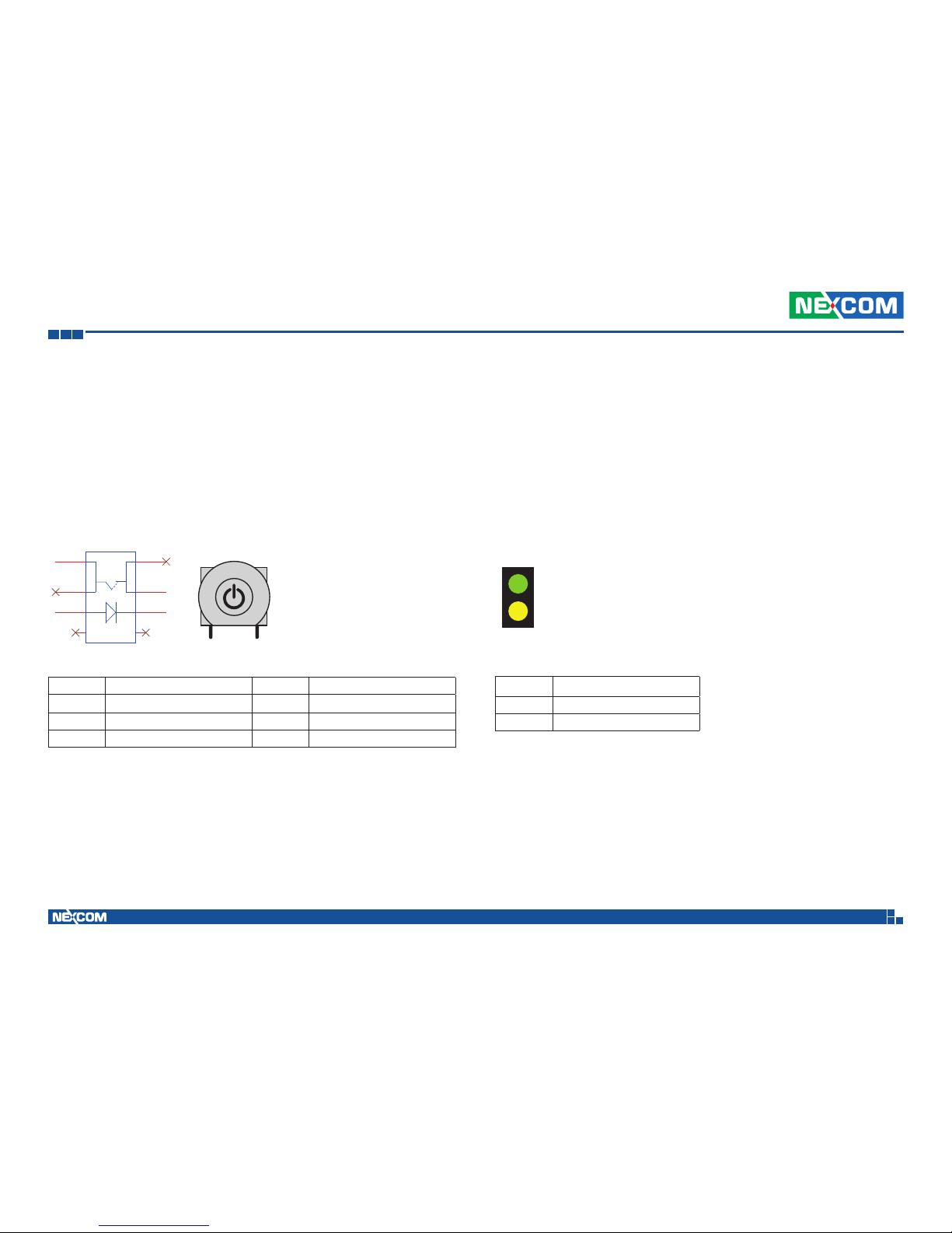
Power Button
Connector Number: 1
Pin Definition Pin Definition
1 GND 2 NC
3 +V3.3ALW 4 NC
A1 VCC5_S C1 GND
1
1
3
3
2
2
4
4
A1A1C1
C1
MH1
MH1
MH2
MH2
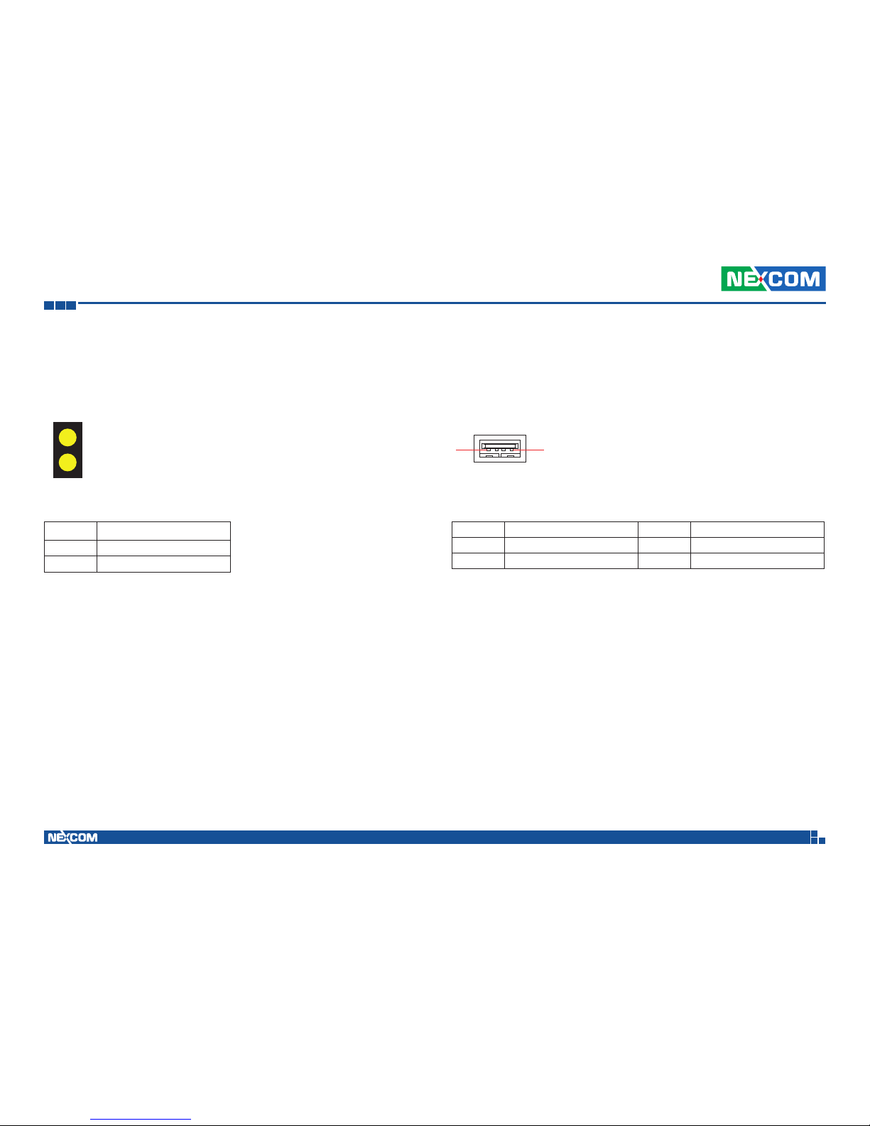
Power On & SSD or HD Active LED
Connector Number: 2
T1
B1
Pin Function Description
T1 POWER LED
B1 HD LED
Page 21
Copyright © 2012 NEXCOM International Co., Ltd. All Rights Reserved.
7
Chapter 2: External Connectors Pinout Description
VTC 7120-BK Series User Manual
USB 2.0 Port
Connector Number: 3
Pin Definition Pin Definition
1 VCC 2 DATA13 DATA1+ 4 GND
1 4
WLAN & WWAN Active LED
Connector Number: 2
Pin Function Description
T1 WWAN LED
B1 WLAN LED
T1
B1
Page 22
Copyright © 2012 NEXCOM International Co., Ltd. All Rights Reserved.
8
Chapter 2: External Connectors Pinout Description
VTC 7120-BK Series User Manual
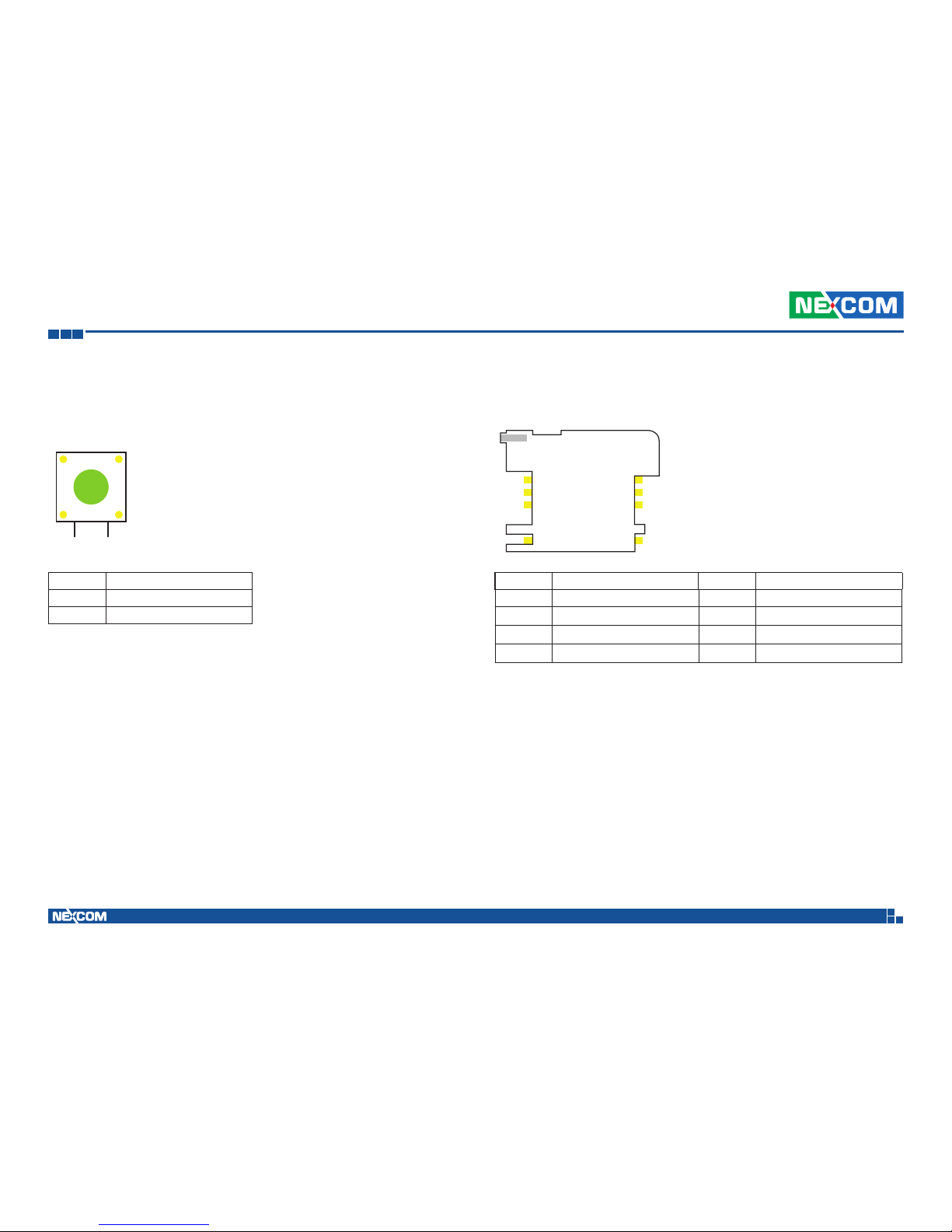
Reset Button
Connector Number: 4
1 2
Pin Function Description
1 GND
2 RST_BTN#
SIM Card Connector-3.5G Wakeup
Connector Number: 5
C5
C6
C7
SW SW
C1
C2
C3
Pin Definition Pin Definition
C1 POWER VOLTAGE C2 RESET SIGNAL
C3 CLOCK SIGNAL C5 GND
vedC6 VPP:PROGRAM VOLTAGE C7 I/O
SW Contact present switch
NOTE: Only SIM CARD 1 (top side) can support SMS wake up function with CM8000 WWAN module.
Page 23
Copyright © 2012 NEXCOM International Co., Ltd. All Rights Reserved.
9
Chapter 2: External Connectors Pinout Description
VTC 7120-BK Series User Manual
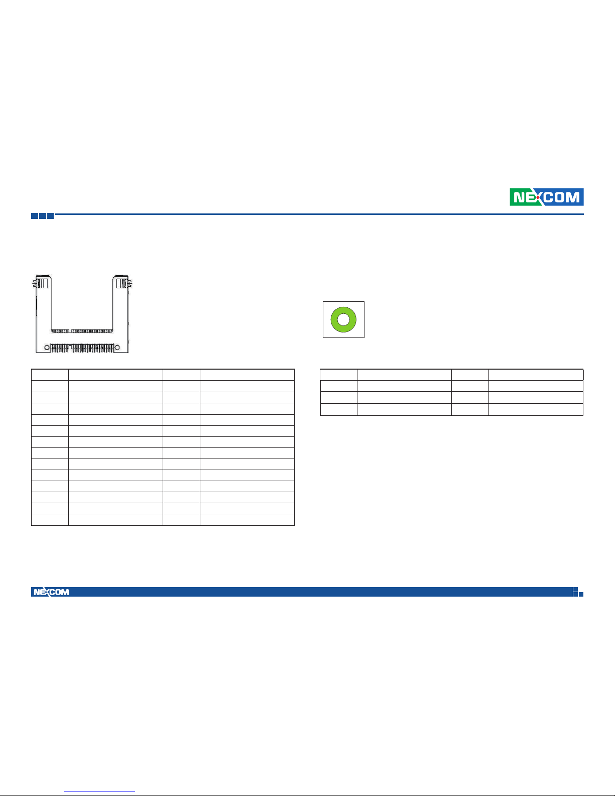
CFast Card Connector
Connector Number: 7
Pin Definition Pin Definition
S1 GND S2 SATA_TXP
S3 SATA_TXN S4 GND
S5 SATA_RXN S6 SATA_RXP
S7 GND
PC1 CFAST_CDI PC2 GND
PC3 NC PC4 NC
PC5 NC PC6 NC
PC7 GND PC8 CFAST_LED1
PC9 CFAST_LED2 PC10 NC
PC11 NC PC12 NC
PC13 VCC3 PC14 VCC3
PC15 GND PC16 GND
PC17 CFAST_CDO
S1 S7 PC1 PC17
Line-out
Connector Number: 8
Pin Definition Pin Definition
1 FRONT_OUT_RC 2 FRONT_JD
3 NC 4 FRONT_OUT_LC
5 GND 6 GND
Page 24
Copyright © 2012 NEXCOM International Co., Ltd. All Rights Reserved.
10
Chapter 2: External Connectors Pinout Description
VTC 7120-BK Series User Manual
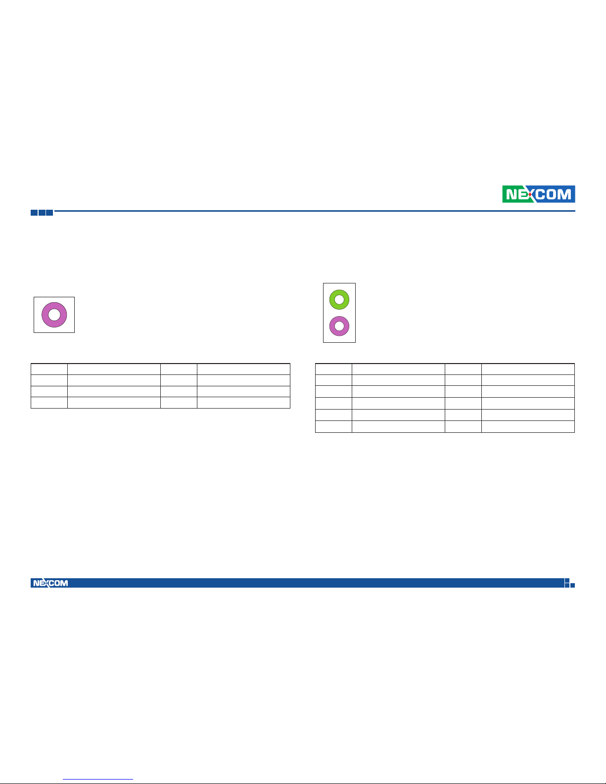
Mic-in
Connector Number: 8
Pin Definition Pin Definition
1 NC 2 MIC_JD
3 NC 4 MIC_OUT-L
5 GND 6 GND
Mic-in2, Line-out2
Connector Number: 9
Pin Definition Pin Definition
1 LINE_OUT_L 2 SURR_JD
3 NC 4 LINE_OUT_R
5 GND 6 GND
22 GND 23 NC
24 MIC_JD 25 MIC_OUT
Page 25
Copyright © 2012 NEXCOM International Co., Ltd. All Rights Reserved.
11
Chapter 2: External Connectors Pinout Description
VTC 7120-BK Series User Manual
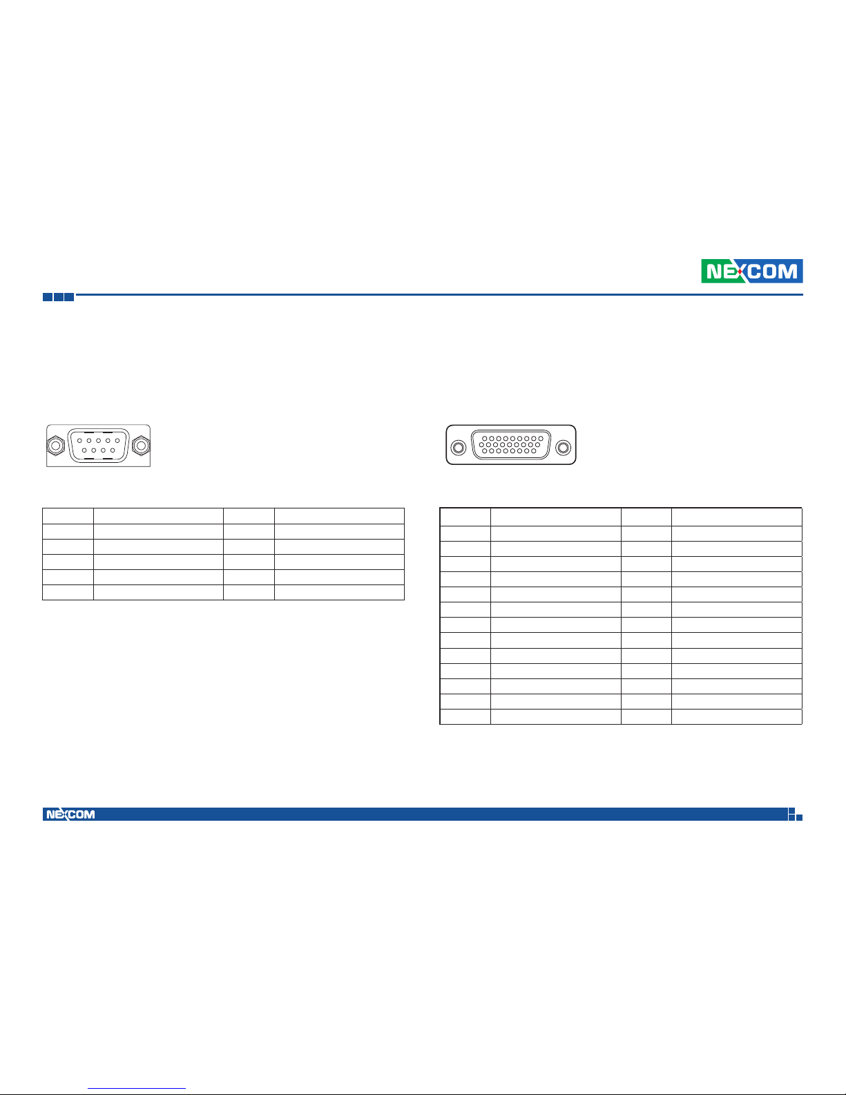
LVDS Connector
Connector size: DB26, Female
Connector Number: 12
19
1926
Pin Definition Pin Definition
1 Panel_ EN 2 Panel_control
3 VDD 4 VDD
5 LCDD09(OUT3) 6 LCDD01(OUT0)
7 LCDD08(OUT3#) 8 LCDD00(OUT0#)
9 LCDD_GND 10 LCDD_GND
11 LCDD07(CLK) 12 LCDD03(OUT1)
13 LCDD06(CLK#) 14 LCDD02(OUT1#)
15 LVDS_GND 16 LCDD_GND
17 LCDD05(OUT2) 18 Power on push button
19 LCDD04(OUT2#) 20 Panel_backlight
21 LCDD_GND 22 Panel-Gnd
23 USB_0# 24 Contact_DET#
25 USB_0 26 USB_VCC
NOTE: maximum resolution up to 1280x768 @ 60Hz
RS232 Connector
Connector size: DB9, Male
Connector Number: 11
Pin Definition Pin Definition
1 DCD 2 RXD
3 TXD 4 DTR
5 GND 6 DSR
7 RTS 8 CTS
9 RI
1 5
9 6
Page 26
Copyright © 2012 NEXCOM International Co., Ltd. All Rights Reserved.
12
Chapter 2: External Connectors Pinout Description
VTC 7120-BK Series User Manual
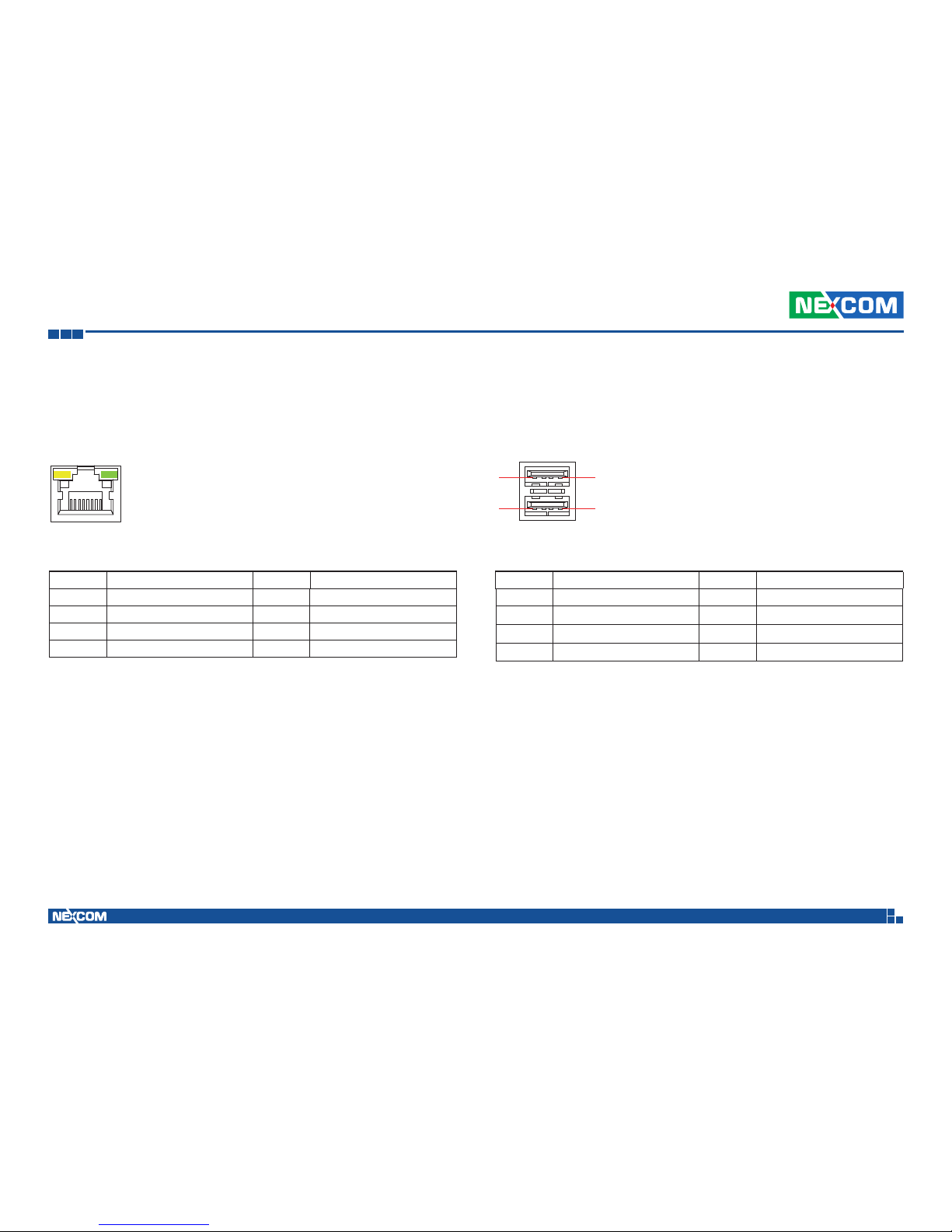
LAN Connectors
Connector size: RJ-45
Connector Number: 14
Pin Definition Pin Definition
1 TX+ 2 TX3 RX+ 4 N/C1
5 N/C2 6 RX7 N/C3 8 N/C4
18
USB Connector
Connector Number: 15
1 4
5 8
Pin Definition Pin Definition
1 VCC 2 DATA1-
3 DATA1+ 4 GND
5 VCC 6 DATA -
7 DATA+ 8 GND
Page 27
Copyright © 2012 NEXCOM International Co., Ltd. All Rights Reserved.
13
Chapter 2: External Connectors Pinout Description
VTC 7120-BK Series User Manual
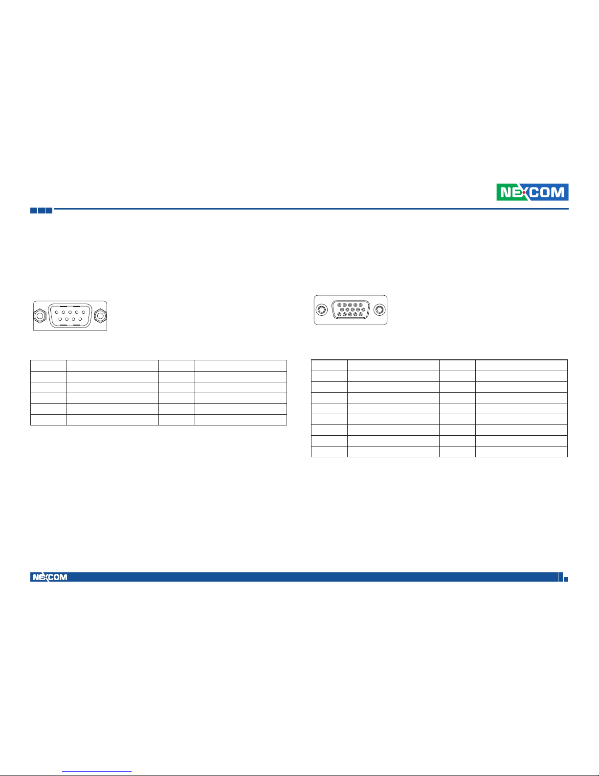
RS422/485 Connector
Connector size: DB9, Male
Connector Number: 16
Pin Definition Pin Definition
1 RS422_RX+ / RS485_+ 2 RS422_RX- / RS485_3 RS422_TX+ 4 RS422_TX5 GND 6 NC
7 NC 8 NC
9 NC
1 5
9 6
5 1
15 11
VGA Connector
Connector size: DB15, Male
Connector Number: 17
Pin Definition Pin Definition
1 RED 2 GREEN
3 BLUE 4 Gnd
5 Gnd 6 Gnd
7 Gnd 8 Gnd
9 VCC 10 Gnd
11 Gnd 12 DDCDAT
13 Hsync 14 Vsync
15 DDCCLK 16 OPEN
Page 28
Copyright © 2012 NEXCOM International Co., Ltd. All Rights Reserved.
14
Chapter 2: External Connectors Pinout Description
VTC 7120-BK Series User Manual
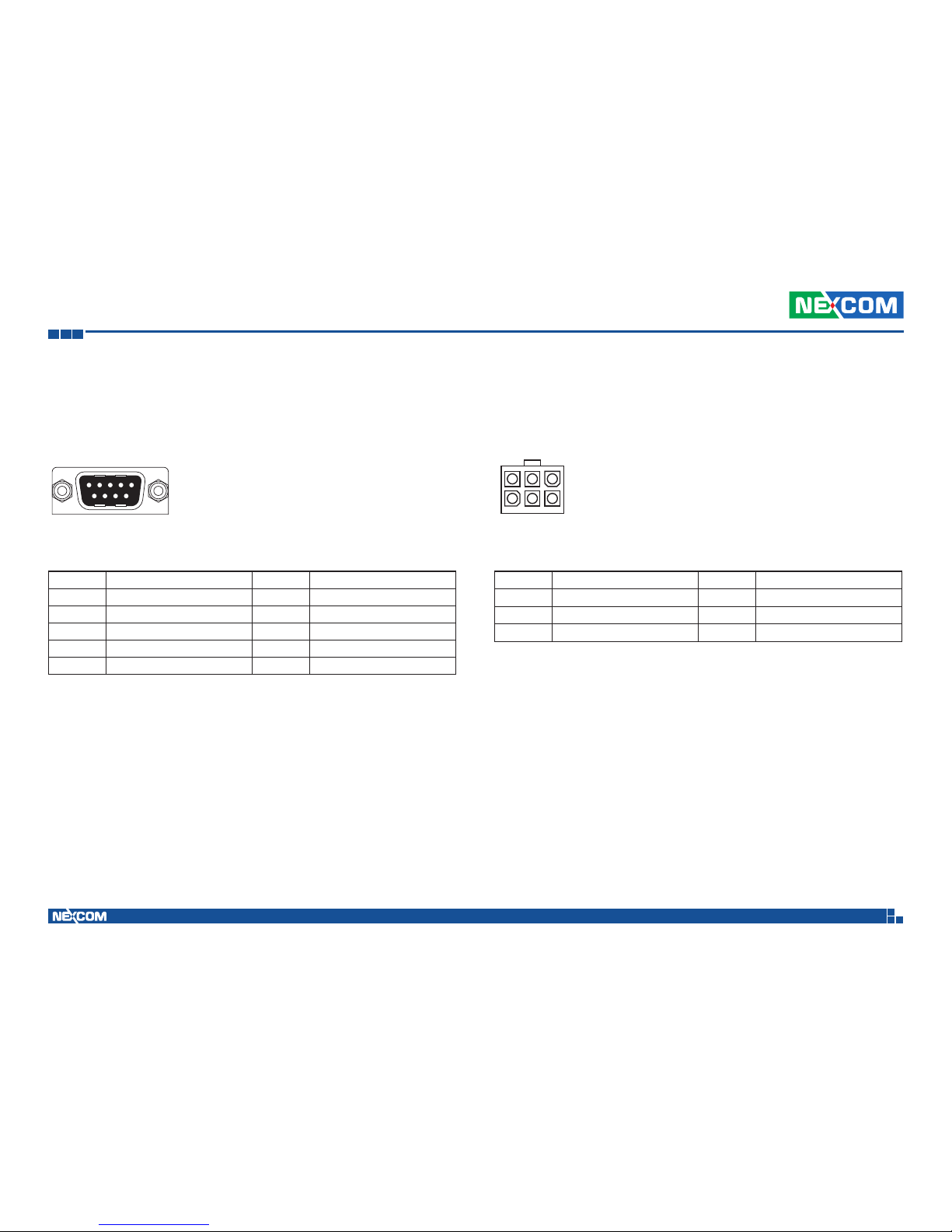
GPIO Connector
Connector size: DB9, Female
Connector Number: 18
Pin Definition Pin Definition
1 INPUT_1 PORT 2 INPUT_2 PORT
3 INPUT_3 PORT 4 INPUT_4 PORT
5 GND 6 OUTPUT_1 PORT
7 OUTPUT_2 PORT / 8 OUTPUT_3 PORT
9 OUTPUT_4 PORT
1 5
8 6
External 12V (4A) & Car Battery (4A) Power and SMBUS
Connector Number: 19
Pin Definition Pin Definition
1 Car battery(4A) 2 VCC12(4A)
3 SMBCLK 4 GND
5 GND 6 SMBDATA
6 4
3 1
Page 29
Copyright © 2012 NEXCOM International Co., Ltd. All Rights Reserved.
15
Chapter 2: External Connectors Pinout Description
VTC 7120-BK Series User Manual
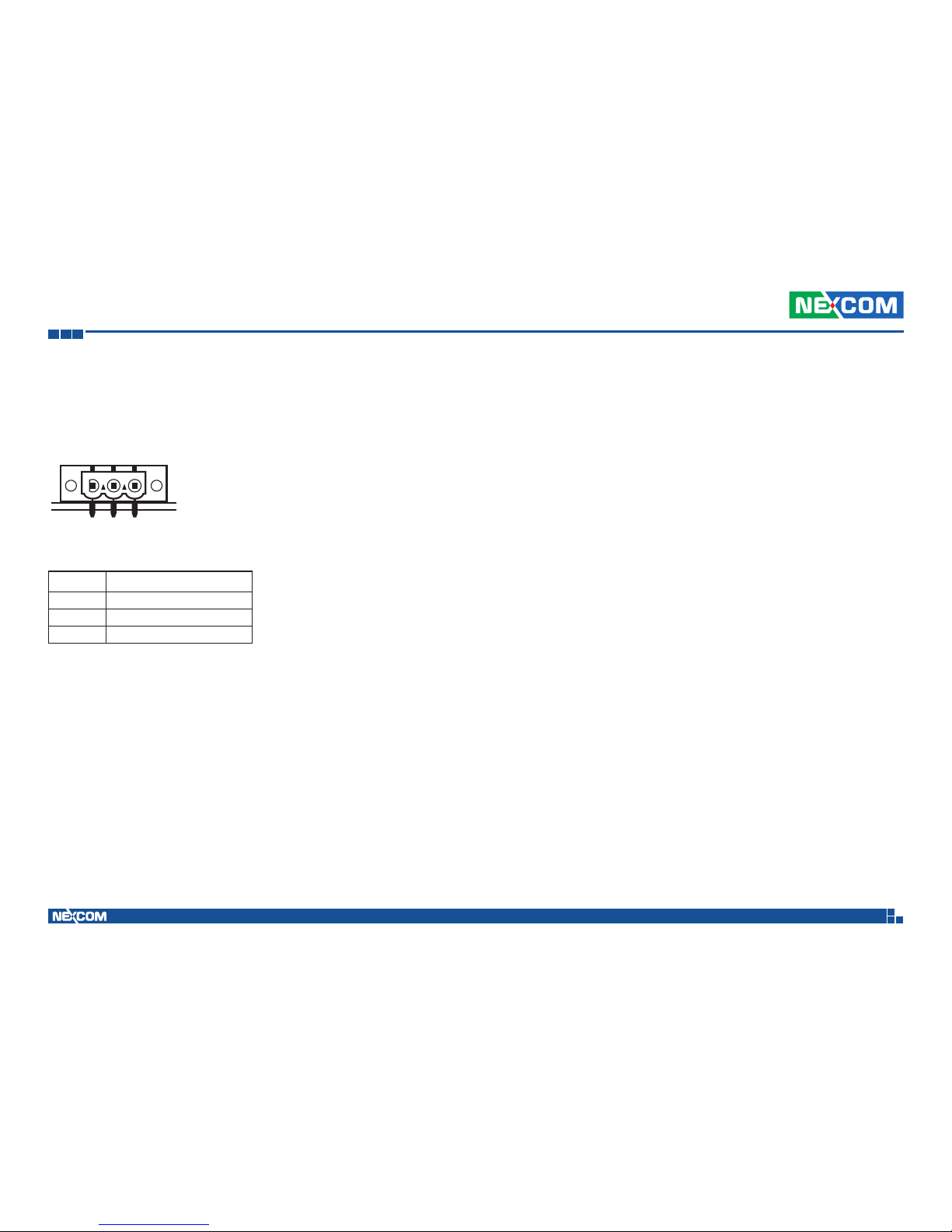
Power Input
Connector size: 3W3 3PIN 6.85mm DIP
Connector Number: 23
Pin Definition
1 GND
2 VIN
3 IGNITION
3 2 1
Page 30

Copyright © 2012 NEXCOM International Co., Ltd. All Rights Reserved.
16
Chapter 3: Jumpers and Switches
VTC 7120-BK Series User Manual
Chapter 3: Jumpers and Switches
This chapter describes how to set the jumpers on the motherboard. Note
that the following procedures are generic for all VTC 7120-BK series.
Before You Begin
▪ Ensure you have a stable, clean working environment. Dust and dirt can
get into components and cause a malfunction. Use containers to keep
small components separated.
▪ Adequate lighting and proper tools can prevent you from accidentally
damaging the internal components. Most of the procedures that follow
require only a few simple tools, including the following:
– A Philips screwdriver
– A flat-tipped screwdriver
– A set of jewelers screwdrivers
– A grounding strap
– An anti-static pad
▪ Using your fingers can disconnect most of the connections. It is
recommended that you do not use needle-nosed pliers to disconnect
connections as these can damage the soft metal or plastic parts of the
connectors.
▪ Before working on internal components, make sure that the power is off.
Ground yourself before touching any internal components, by touching
a metal object. Static electricity can damage many of the electronic
components. Humid environment tend to have less static electricity than
dry environments. A grounding strap is warranted whenever danger of
static electricity exists.
Precautions
Computer components and electronic circuit boards can be damaged by
discharges of static electricity. Working on the computers that are still
connected to a power supply can be extremely dangerous.
Follow the guidelines below to avoid damage to your computer or yourself:
▪ Always disconnect the unit from the power outlet whenever you are
working inside the case.
▪ If possible, wear a grounded wrist strap when you are working inside the
computer case. Alternatively, discharge any static electricity by touching
the bare metal chassis of the unit case, or the bare metal body of any
other grounded appliance.
▪ Hold electronic circuit boards by the edges only. Do not touch the
components on the board unless it is necessary to do so. Don’t flex or
stress the circuit board.
▪ Leave all components inside the static-proof packaging that they shipped
with until they are ready for installation.
▪ Use correct screws and do not over tighten screws.
Page 31
Copyright © 2012 NEXCOM International Co., Ltd. All Rights Reserved.
17
Chapter 3: Jumpers and Switches
VTC 7120-BK Series User Manual
Jumper Settings
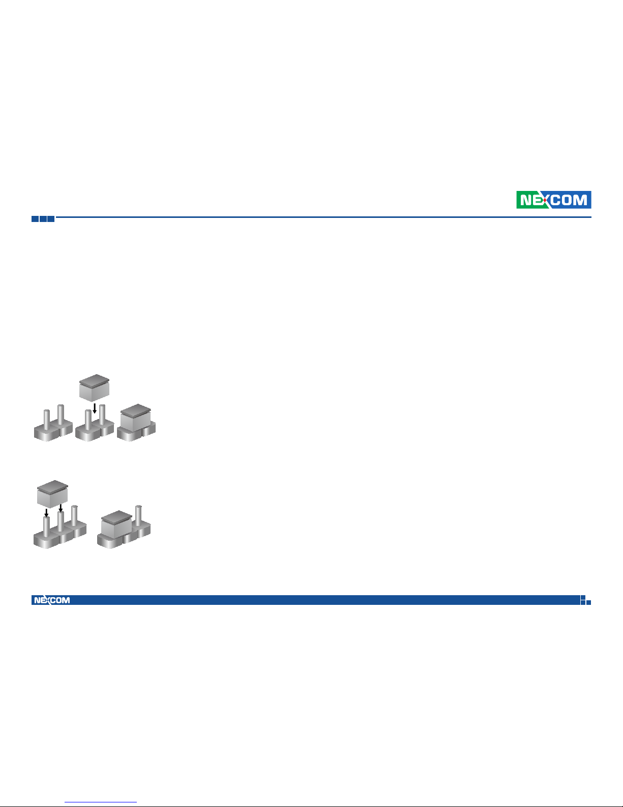
A jumper is the simplest kind of electric switch. It consists of two metal
pins and a cap. When setting the jumpers, ensure that the jumper caps are
placed on the correct pins. When the jumper cap is placed on both pins, the
jumper is short. If you remove the jumper cap, or place the jumper cap on
just one pin, the jumper is open.
Refer to the illustrations below for examples of what the 2-pin and 3-pin
jumpers look like when they are short (on) and open (off).
Two-Pin Jumpers: Open (Left) and Short (Right)
Three-Pin Jumpers: Pins 1 and 2 are Short
1
2
3
1
2
3
Page 32
Copyright © 2012 NEXCOM International Co., Ltd. All Rights Reserved.
18
Chapter 3: Jumpers and Switches
VTC 7120-BK Series User Manual
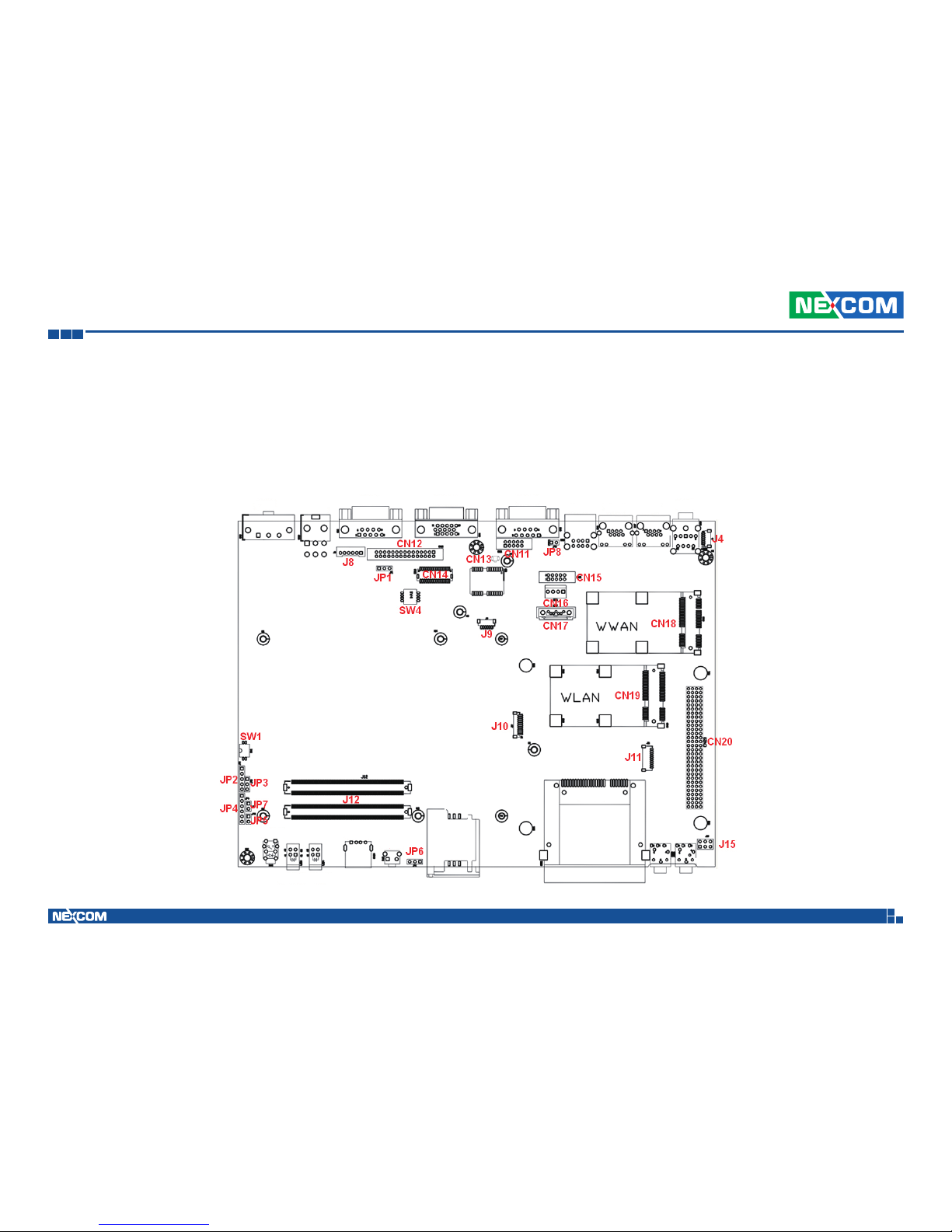
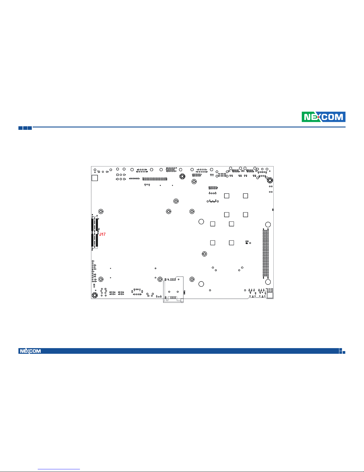
VTC 7120-BK Series Connector Specification & Jumper Setting
Carrier board placement
The figure below is the carrier board which is the board used in the system. It shows the locations of the jumpers and connectors.
Top View
Page 33
Copyright © 2012 NEXCOM International Co., Ltd. All Rights Reserved.
19
Chapter 3: Jumpers and Switches
VTC 7120-BK Series User Manual
Bottom View
Page 34
Copyright © 2012 NEXCOM International Co., Ltd. All Rights Reserved.
20
Chapter 3: Jumpers and Switches
VTC 7120-BK Series User Manual
VTC 7120-BK Jumpers Setting
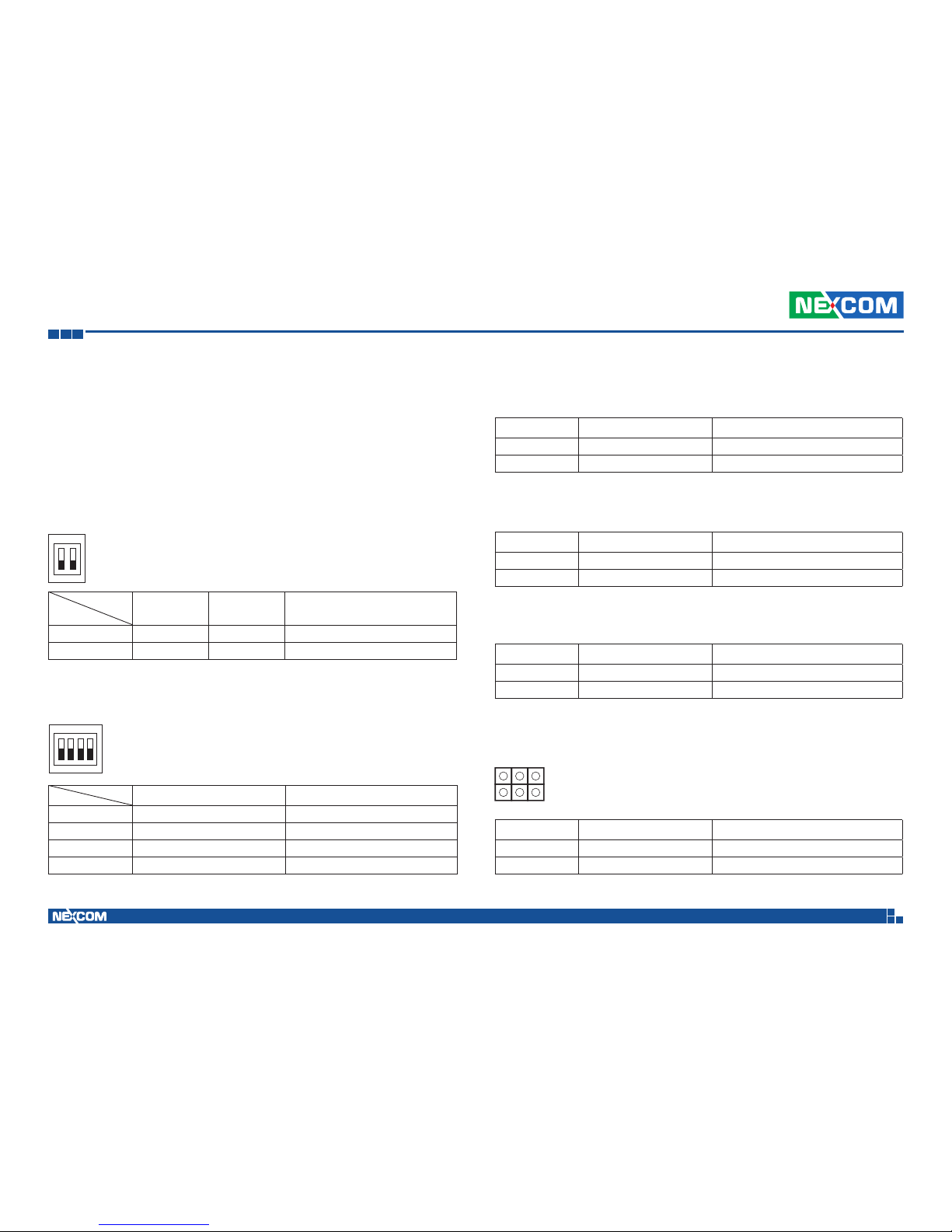
CMOS Clear Select
SW2: Power-on Button
SW3: Reset Button
Item B. Start-up & Shut down voltage control
(*) for default seeting
SW1: Voltage setup selection
12V 24V
9V~36V (*)
all can start
SW1.1 OFF OFF ON
SW1.2 OFF ON Don’t Care
RS232 – Enable Select
Connector location: JP8
Pin Status Function Description
1-2 Short Disable RS232
1-2(*) NC Enable RS232
2
1
N
O
SW4: Voltage setup selection
214
3
N
O
ON(*) OFF
SW4.1 GPO0 PULL UP 5V Don’t Care
SW4.2 GPO1 PULL UP 5V Don’t Care
SW4.3 GPO2 PULL UP 5V Don’t Care
SW4.4 GPO3 PULL UP 5V Don’t Care
SW1
setup voltage
SW1
setup voltage
LVDS Power input Voltage Select
Connector location: JP1
Pin Status Function Description
1-2 Short +5V IN
2-3(*) Short* +3.3V IN
CMOS Input Voltage Select
Connector location: JP6
Pin Status Function Description
1-2(*) Short* VBAT IN
2-3 Short Clear CMOS
PCI-104 VI/O Voltage Setting
Connector location: J15
Pin Status Function Description
(1-3)(2-4) (*) Short +3.3V
(3-5)(4-6) Short +5V
2 4 6
1 3 5
Page 35
Copyright © 2012 NEXCOM International Co., Ltd. All Rights Reserved.
21
Chapter 3: Jumpers and Switches
VTC 7120-BK Series User Manual
RS232 Connector
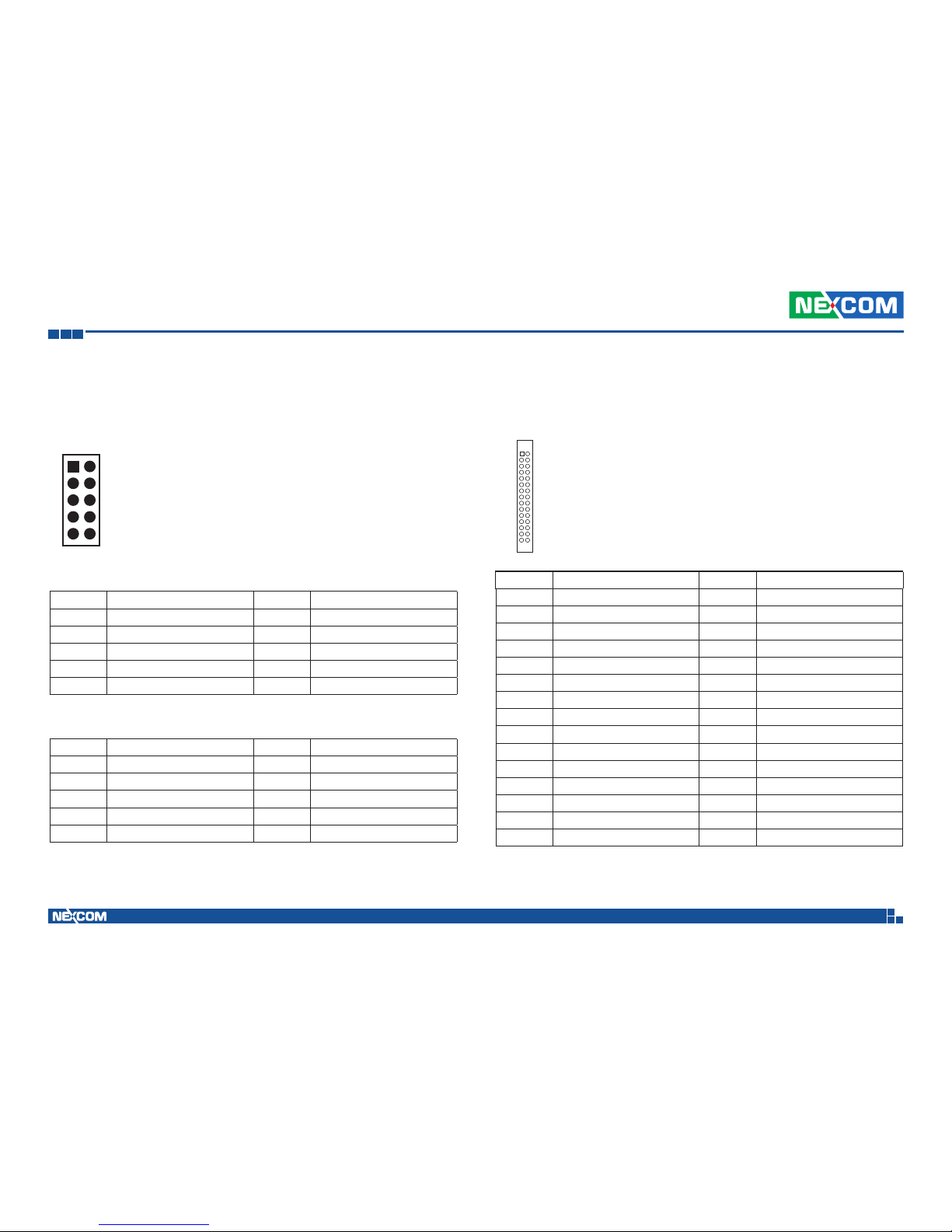
Connector size:2 x 5 = 10Pins PIN Header, ( 2.0 mm Pitch )
Connector location: CN11, CN15
(CN15USE TTL SINGNAL)
Pin Definition Pin Definition
1 VCC5 2 VCC12
3 NC 4 NC
5 GND 6 GND
7 CAN_DI 8 CAN_DO
9 TXD1 10 RXD1
(CN11Standard RS232 interface)
Pin Definition Pin Definition
1 DCD1 2 RXD1
3 TXD1 4 DTR1
5 Gnd1 6 DSR1
7 RTS1 8 CTS1
9 RI1
1
9
2
LVDS Connector+USB0
Connector size: 2 X 15 (2.0mm)
Connector location: CN12
21
3029
Pin Definition Pin Definition
1 LVDS_CLK 2 LVDS_DAT
3 Panel_VDD 4 LVDS_1(OUT0)
5 LVDS_9(OUT3) 6 LVDS_0(OUT0#)
7 LVDS_8(OUT3#) 8 Panel_VDD
9 LVDS_GND 10 LVDS_GND
11 LVDS_7(CLK) 12 LVDS_3(OUT1)
13 LVDS_6(CLK#) 14 LVDS_2(OUT1#)
15 LVDS_GND 16 LVDS_GND
17 LVDS_5(OUT2) 18 Panel_backlight(+12V)
19 LVDS_4(OUT2#) 20 Panel_backlight(+12V)
21 LVDS_GND 22 Power on push buttom
23 USB_2# 24 USB_GND
25 USB_2 26 USB_VCC (+5V)
27 USB_GND 28 USB_GND
29 Panel_backlight(+12V) 30 GND
Page 36
Copyright © 2012 NEXCOM International Co., Ltd. All Rights Reserved.
22
Chapter 3: Jumpers and Switches
VTC 7120-BK Series User Manual
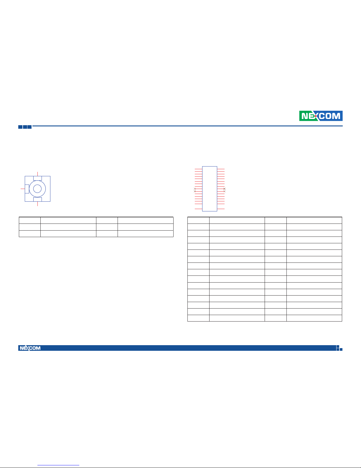
GPS I-PEX Connector
Connector location: CN13
Pin Definition Pin Definition
1 RF_IN_F 2 GND
3 GND 4
1
32
DVI+VGA Connector
Connector size: 2 x 15 = 30Pins PIN Header, ( 1.0 mm Pitch )
Connector location: CN14
Pin Definition Pin Definition
1 CH_CLK_N 2 DVI_I_5V
3 CH_CLK_P 4 HPDET_I
5 CH_TX0_N 6 DVI_I_DDC_D_R
7 CH_TX0_P 8 DVI_I_DDC_C_R
9 CH_TX1_N 10 CH_GND
11 CH_TX1_P 12 CH_GND
13 CH_TX2_N 14 CH_GND
15 CH_TX2_P 16 CH_GND
17 NC 18 NC
19 NC 20 NC
21 CH_GND 22 VGA1_HSYNC
23 VGA1_RED 24 VGA1_VSYNC
25 VGA1_BLUE 26 VGA1_DDCDAT
27 VGA1_GREEN 28 VGA1_DDCCLK
29 M_DET 30 VGA1_PWR_L
1
3
5
7
9
11
13
15
17
19
21
23
25
27
29
2
4
6
8
10
12
14
16
18
20
22
24
26
28
30
GND GN D
1
3
5
7
9
11
13
15
17
19
21
23
25
27
29
2
4
6
8
10
12
14
16
18
20
22
24
26
28
30
MH1 MH2
Page 37
Copyright © 2012 NEXCOM International Co., Ltd. All Rights Reserved.
23
Chapter 3: Jumpers and Switches
VTC 7120-BK Series User Manual
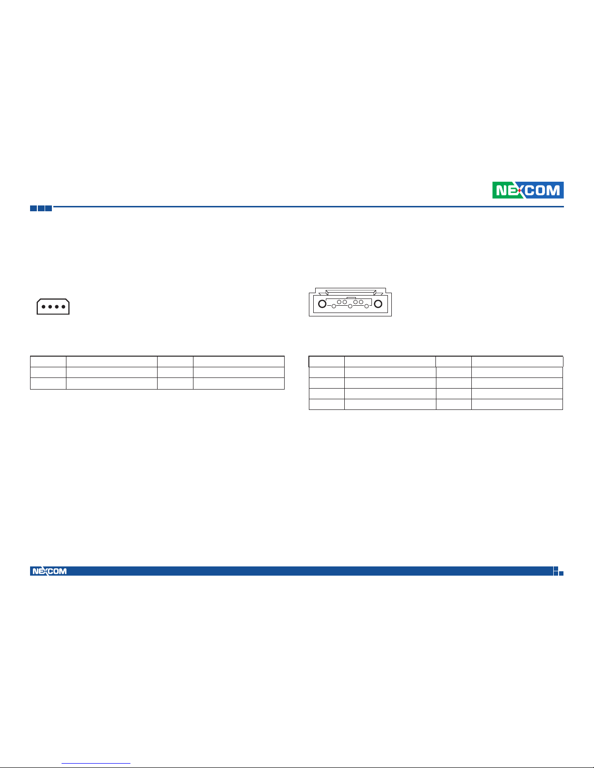
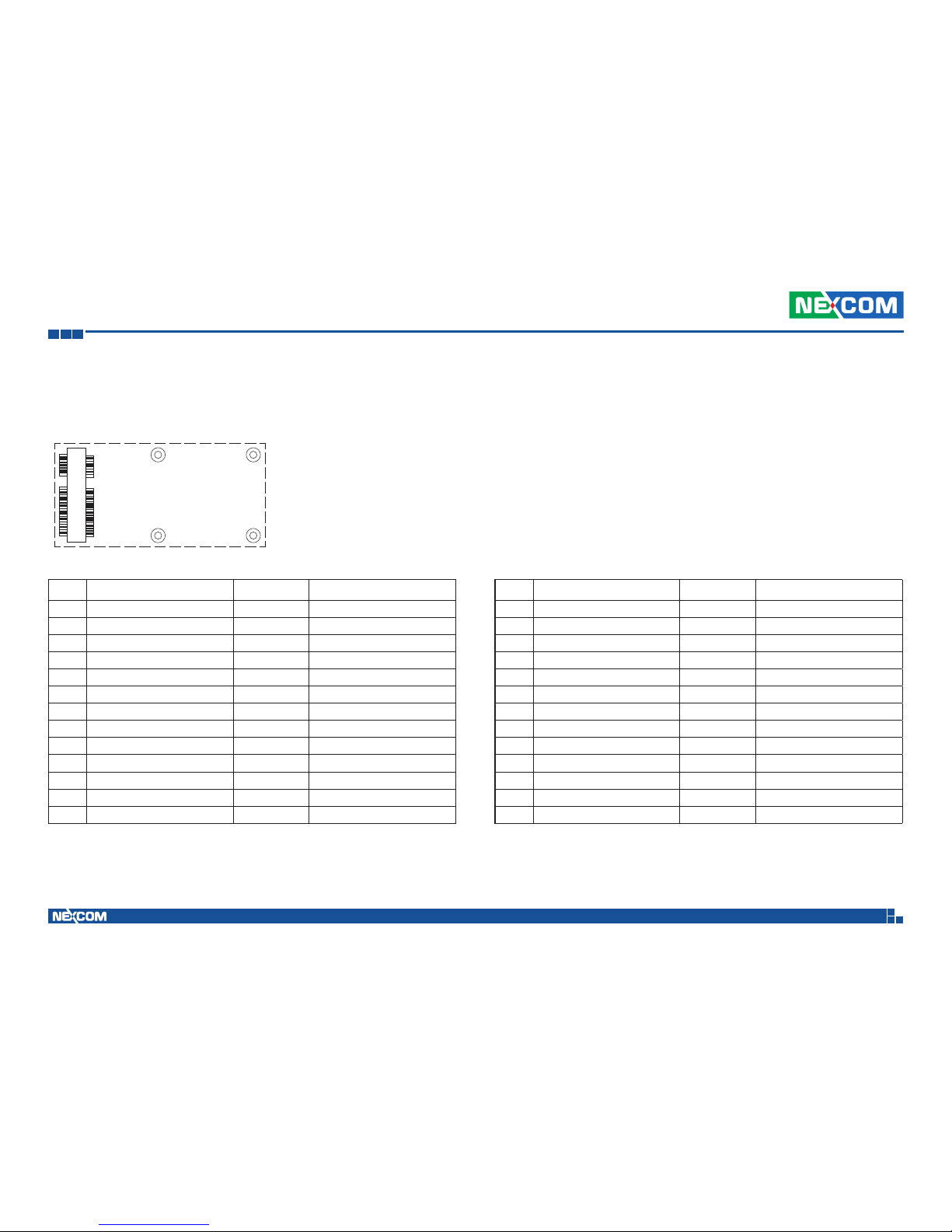
SATA PWR Connector
Connector location: CN16
14
Pin Definition Pin Definition
1 VCC12 2 GND
3 GND 4 VCC5
SATA Connector
Connector location: CN17
Pin Definition Pin Definition
1 GND 2 SATA_TXP0 3 SATA_TXN0 4 GND
5 SATA_RXN0 6 SATA_RXP0
7 GND
Page 38
Copyright © 2012 NEXCOM International Co., Ltd. All Rights Reserved.
24
Chapter 3: Jumpers and Switches
VTC 7120-BK Series User Manual
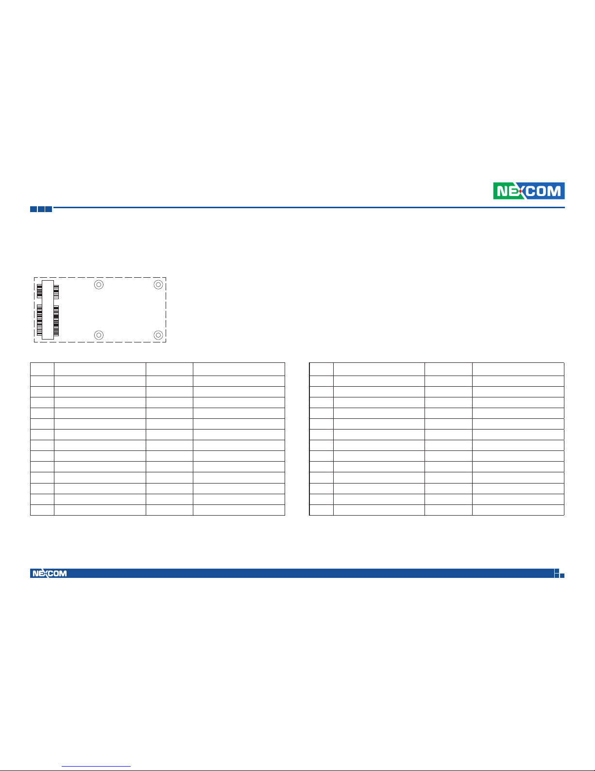
Mini-PCIe (WWAN)
Connector location: CN18
1 2
51 52
Pin Definition Pin Definition
1 MIC + 2 +V3.3S
3 MIC - 4 GND
5 SPK + 6 NC
7 GND 8 USIM PWR
9 GND 10 USIM DATa
11 VCC_MSM26_DIG 12 USIM CLK
13 NC 14 USIM RST
15 GND 16 NC
17 NC 18 GND
19 NC 20 W_DISABLE#
21 GND 22 NC
23 NC 24 NC
25 NC 26 GND
Pin Definition Pin Definition
27 GND 28 NC
29 GND 30 NC
31 NC 32 NC
33 RESET 34 GND
35 GND 36 USB_D37 GND 38 USB_D+
39 +V3.3S 40 GND
41 +V3.3S 42 LED_WWAN#
43 GND 44 NC
45 NC 46 NC
47 NC 48 NC
49 NC 50 GND
51 NC 52 +V3.3S
Page 39
Copyright © 2012 NEXCOM International Co., Ltd. All Rights Reserved.
25
Chapter 3: Jumpers and Switches
VTC 7120-BK Series User Manual
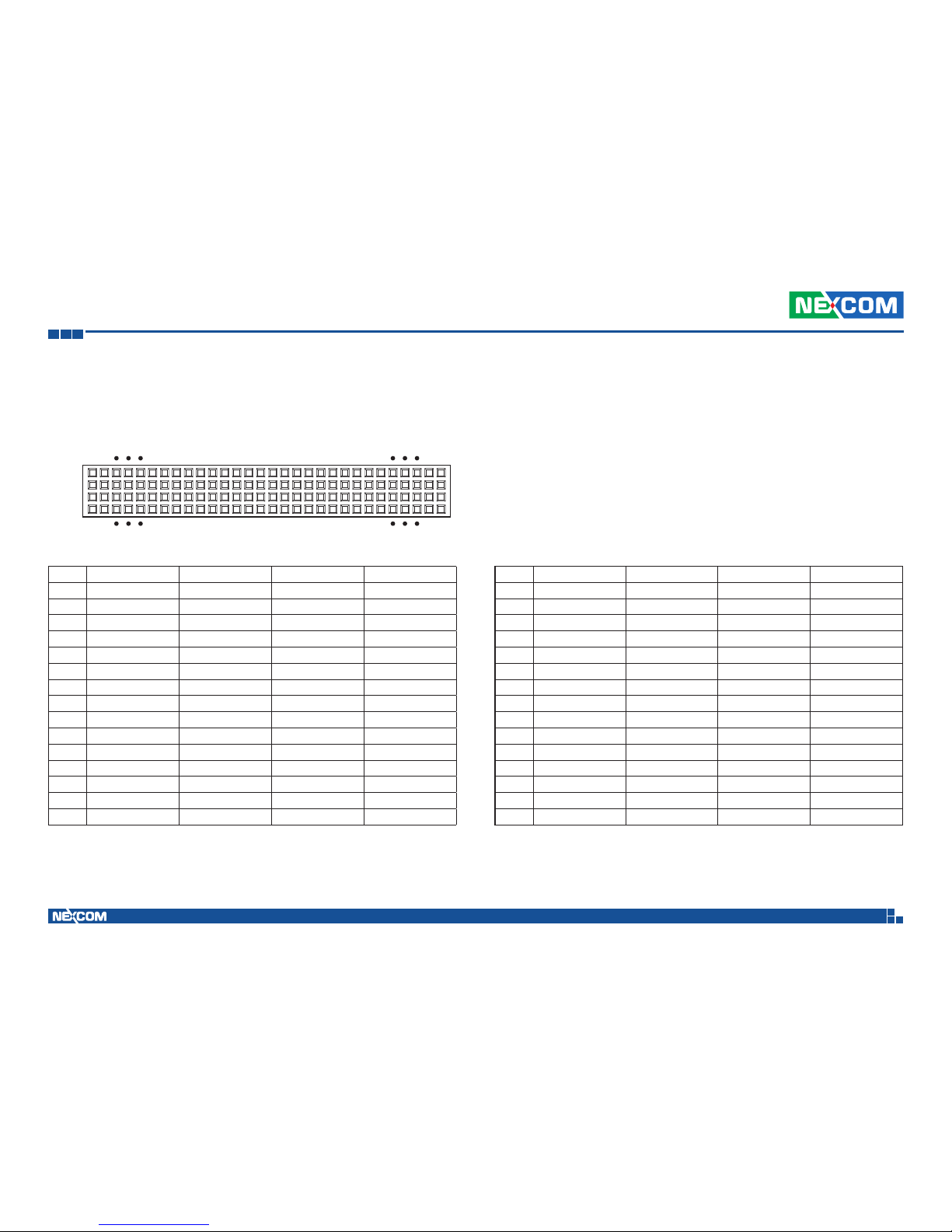
Mini-PCIe (WLAN)
Connector location: CN19
1 2
51 52
Pin Definition Pin Definition
1 WAKE# 2 +V3.3S
3 NC 4 GND
5 NC 6 +V1.5S
7 CLKREQ# 8 NC
9 GND 10 NC
11 REFCLK- 12 NC
13 REFCLK+ 14 NC
15 GND 16 NC
17 NC 18 GND
19 NC 20 DISABLE#
21 GND 22 PERST#
23 PERn0 24 +3.3S
25 PERp0 26 GND
Pin Definition Pin Definition
27 GND 28 +V1.5S
29 GND 30 SMB_CLK
31 PETn0 32 SMB_DATA
33 PETp0 34 GND
35 GND 36 USB_D37 NC 38 USB_D+
39 NC 40 GND
41 NC 42 LED_WWAN#
43 NC 44 LED_WLAN#
45 NC 46 LED_WPAN#
47 NC 48 +V1.5S
49 NC 50 GND
51 NC 52 +V3.3S
Page 40
Copyright © 2012 NEXCOM International Co., Ltd. All Rights Reserved.
26
Chapter 3: Jumpers and Switches
VTC 7120-BK Series User Manual
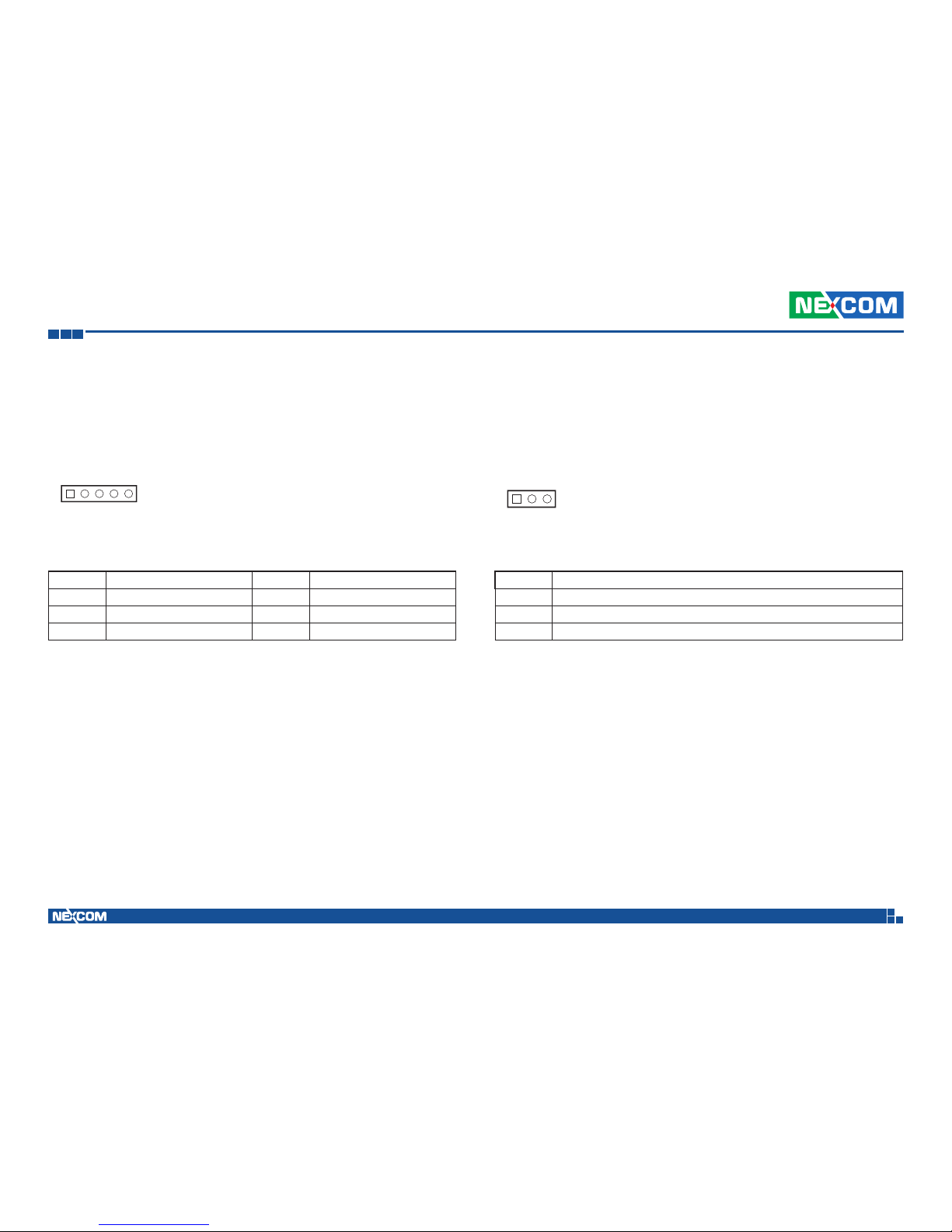
PCI-104 Connector
Connector location: CN20
Pin A B C D
1 GND Reserved +5 AD00
2 VI/O AD02 AD01 +5V
3 AD05 GND AD04 AD03
4 C/BE0# AD07 GND AD06
5 GND AD09 AD08 GND
6 AD11 VI/O AD10 M66EN
7 AD14 AD13 GND AD12
8 +3.3V C/BE1# AD15 +3.3V
9 SERR# GND Reserved PAR
10 GND PERR# +3.3V Reserved
11 STOP# +3.3V LOCK# GND
12 +3.3V TRDY# GND DEVSEL#
13 FRAME# GND IRDY# +3.3V
14 GND AD16 +3.3V C/BE2#
15 AD18 +3.3V AD17 GND
Row A
Row B
Row C
Row D
1 2 29 30
1 2 29 30
Pin A B C D
16 AD21 AD20 GND AD19
17 +3.3V AD23 AD22 +3.3V
18 IDSEL0 GND IDSEL1 IDSEL2
19 AD24 C/BE3# VI/O IDSEL3
20 GND AD26 AD25 GND
21 AD29 +5V AD28 AD27
22 +5V AD30 GND AD31
23 REQ0# GND REQ1# VI/O
24 GND REQ2# +5V GNT0#
25 GNT1# VI/O GNT2# GND
26 +5V CLK0 GND CLK1
27 CLK2 +5V CLK3 GND
28 GND INTD# +5V RST#
29 +12V INTA# INTB# INTC#
30 -12V REQ3# GNT3# GND
Page 41
Copyright © 2012 NEXCOM International Co., Ltd. All Rights Reserved.
27
Chapter 3: Jumpers and Switches
VTC 7120-BK Series User Manual
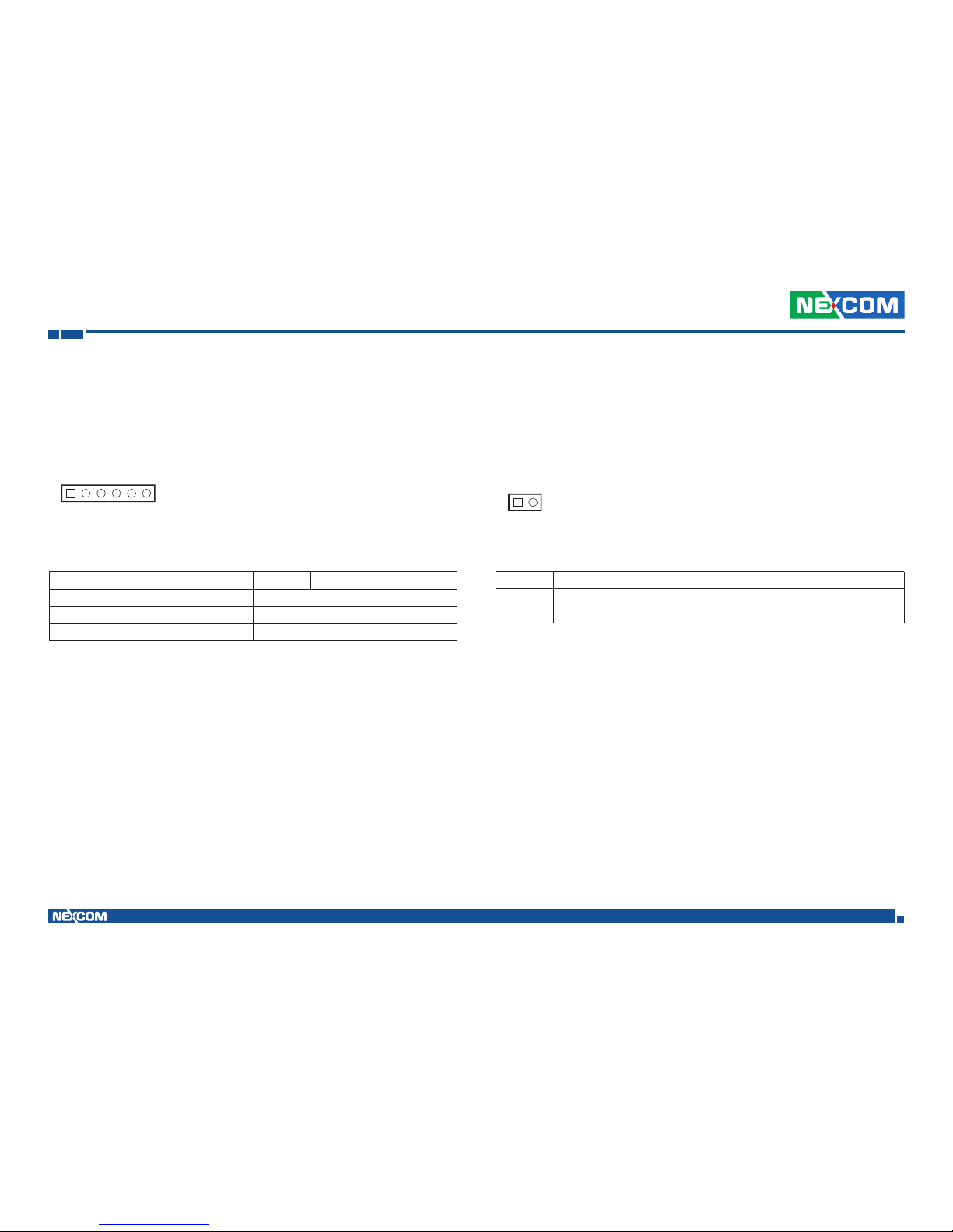
MCU Programmer PIN Header
Connector location: JP2
Pin Definition Pin Definition
1 +3.3ALW 2 C2D
3 MRST 4 C2CK
5 GND
MCU COM Port
Connector location: JP3
Pin Function Description
1 TX
2 RX
3 GND
1 3
1 5
Page 42
Copyright © 2012 NEXCOM International Co., Ltd. All Rights Reserved.
28
Chapter 3: Jumpers and Switches
VTC 7120-BK Series User Manual
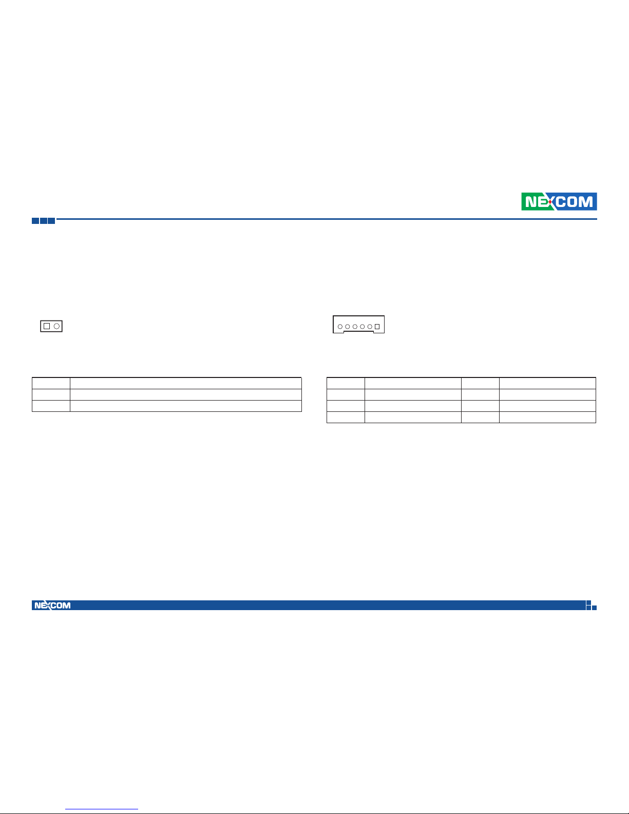
Super I/O Temperature Sensor
Connector location: JP5
Pin Function Description
1 SENSOR+
2 GND
1 2
GAL Programmer PIN Header
Connector location: JP4
Pin Definition Pin Definition
1 VCC3 2 GND
3 TCK 4 TDO
5 TD1 6 TMS
1 6
Page 43
Copyright © 2012 NEXCOM International Co., Ltd. All Rights Reserved.
29
Chapter 3: Jumpers and Switches
VTC 7120-BK Series User Manual
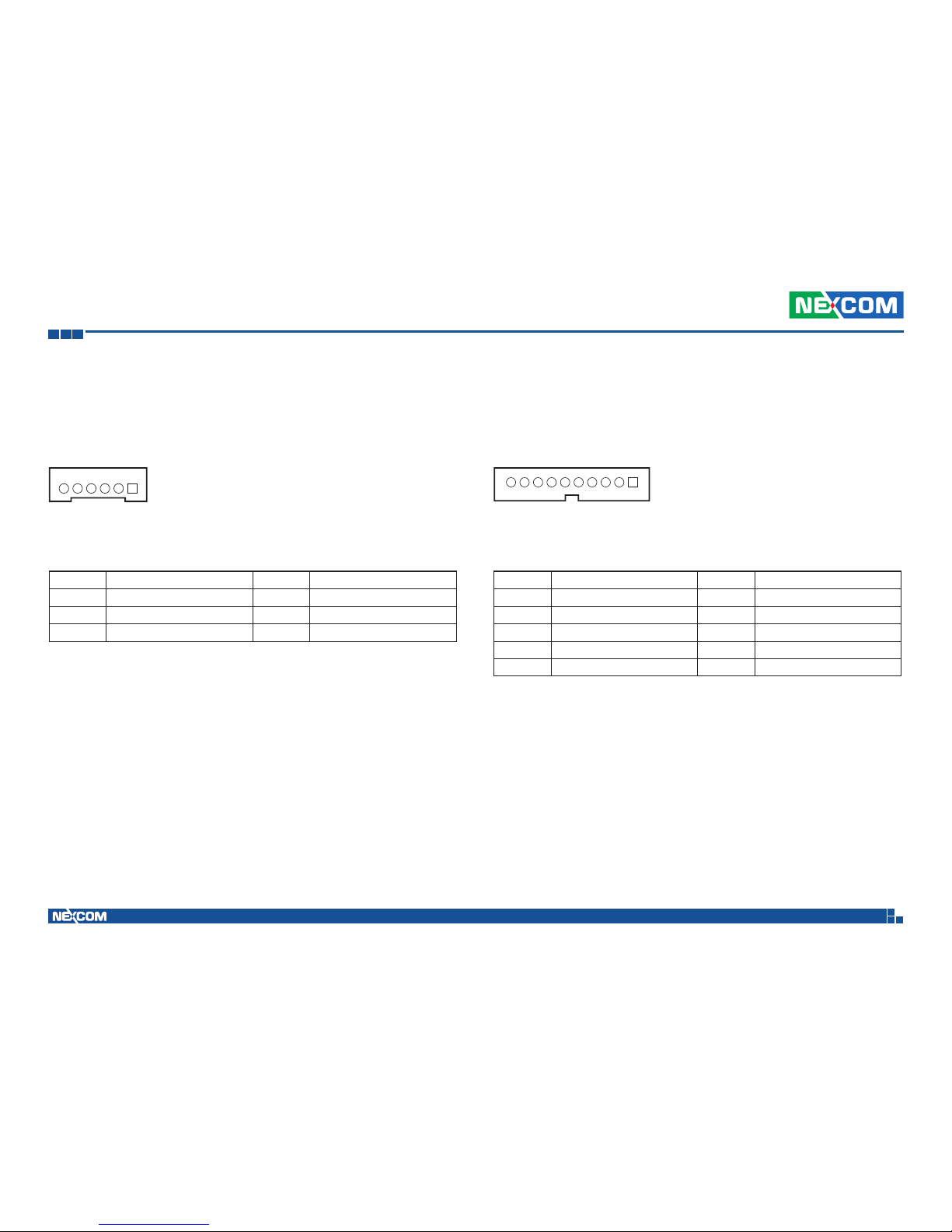
MCU Temperature Sensor
Connector location: JP7
1 2
Pin Function Description
1 SENSOR+
2 GND
LVDS Power Connector
Connector location: J8
16
Pin Definition Pin Definition
1 Panel_backlight 2 Panel_VDD
3 GND 4 GND
5 LVDS_PANEL 6 LVDS_BIASON
Page 44
Copyright © 2012 NEXCOM International Co., Ltd. All Rights Reserved.
30
Chapter 3: Jumpers and Switches
VTC 7120-BK Series User Manual
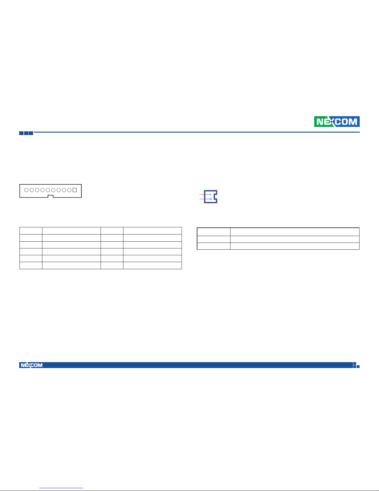
GPS Connector
Connector location: J9
Port80 Connector
Connector location: J10
16
Pin Definition Pin Definition
1 +V3.3S 2 GND
3 SP_RX1 4 SP_TX1
5 GPS_LED# 6 GPS_BAT
110
Pin Definition Pin Definition
1 GND 2 CB_RESET#
3 SIO_CLK 4 LPC_FRAME#
5 LPC_AD3 6 LPC_AD2
7 LPC_AD1 8 LPC_AD0
9 VCC3 10 VCC3
NOTE: Onboard uBlox NEO-6Q GPS module can’t be used with optional GPS dead reckoning module
(VIOB-GPS-DR01) at the same time.
Page 45
Copyright © 2012 NEXCOM International Co., Ltd. All Rights Reserved.
31
Chapter 3: Jumpers and Switches
VTC 7120-BK Series User Manual
Bluetooth Connector
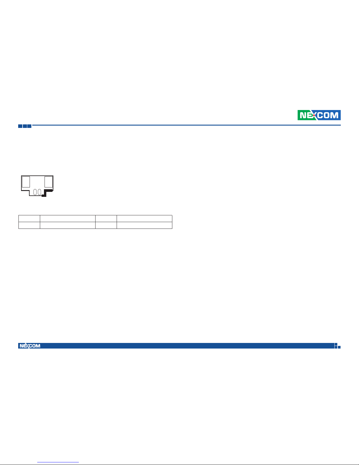
Connector location: J11
Pin Definition Pin Definition
1 GND 2 USB_6P_L
3 USB_6N_L 4 NC
5 NC 6 BT_AUDIO_EN_R
7 NC 8 BT_3.3V
9 NC 10 GND
110
Button Power
Connector location: J13
NO
1
2
Pin Function Description
1 GND
2 3.3V
Page 46
Copyright © 2012 NEXCOM International Co., Ltd. All Rights Reserved.
32
Chapter 3: Jumpers and Switches
VTC 7120-BK Series User Manual
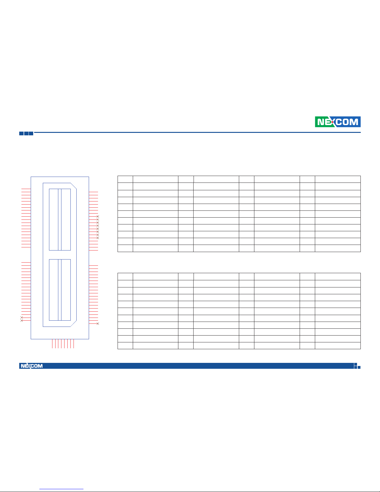
RTC Battery Connector
Connector location: J14
12
Pin Definition Pin Definition
1 GND 2 VBAT1
Page 47
Copyright © 2012 NEXCOM International Co., Ltd. All Rights Reserved.
33
Chapter 3: Jumpers and Switches
VTC 7120-BK Series User Manual
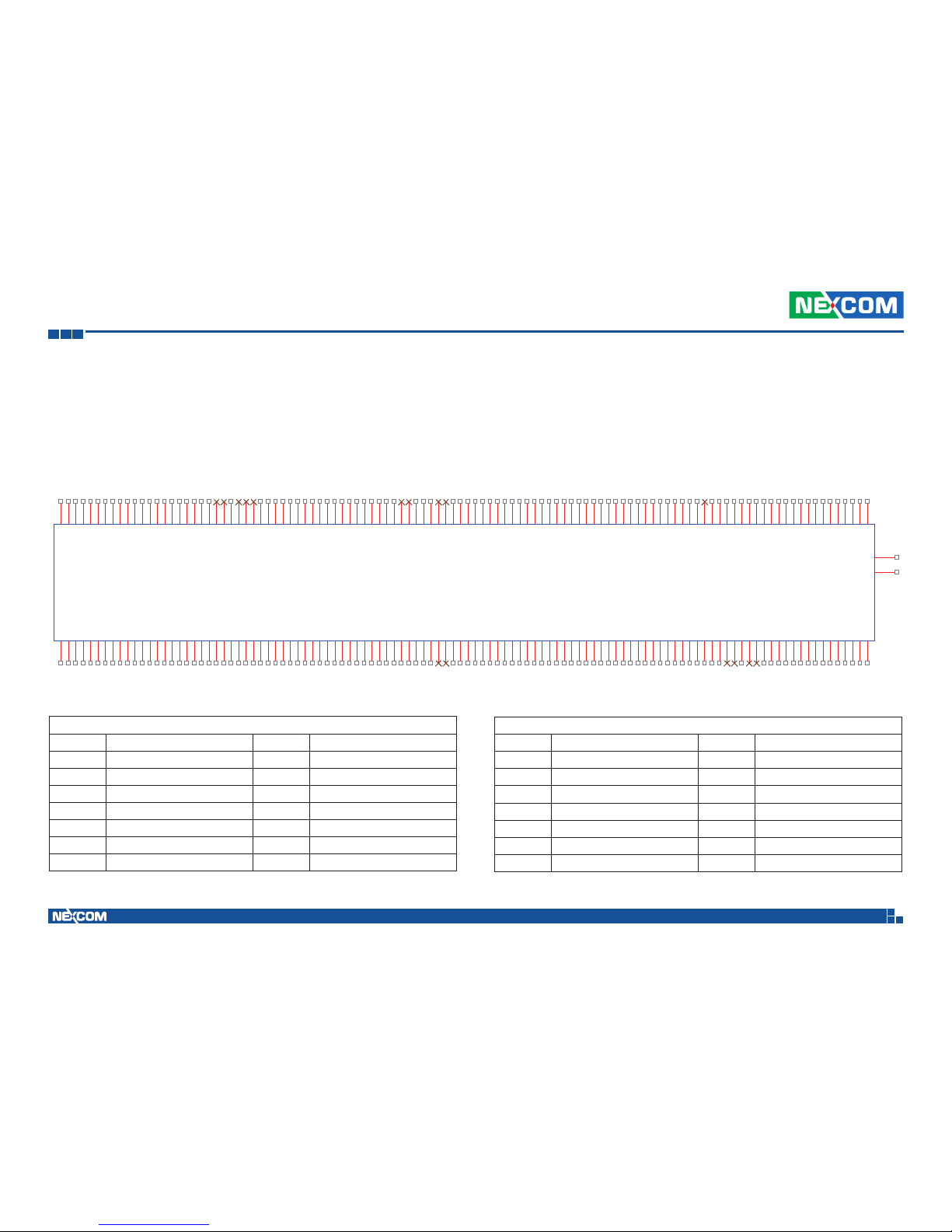
Hi-speed Board to Board Connector
V_MIN= CAR BATTERY OR POE POWER
Connector location: J17
Pin Definition Pin Definition Pin Definition Pin Definition
A1 V_MIN A2 GND A3 V_MIN A4 GND
A5 V_MIN A6 GND A7 V_MIN A8 GND
A9 V_MIN A10 GND A11 V_MIN A12 GND
A13 V_MIN A14 GND A15 V_MIN A16 IGNITION_X
A17 V_MIN A18 A19 V_MIN A20
A21 V_MIN A22 A23 V_MIN A24
A25 V_MIN A26 A27 V_MIN A28
A29 V_MIN A30 A31 V_MIN A32
A33 V_MIN A34 PM_SLP_S5# A35 V_MIN A36 PM_SLP_S4#
A37 V_MIN A38 PM_SLP_S3# A39 V_MIN A40 I/O POK
GND1GND2
A1
A2
A3
A4
A5
A6
A7
A8
A9
A10
A11
A12
A13
A14
A15
A16
A17
A18
A19
A20
A21
A22
A23
A24
A25
A26
A27
A28
A29
A30
A31
A32
A33
A34
A35
A36
A37
A38
A39
A40
B1
B3
B5
B7
B9
B11
B13
B15
B17
B19
B21
B23
B25
B27
B29
B31
B33
B35
B37
B39
B2
B4
B6
B8
B10
B12
B14
B16
B18
B20
B22
B24
B26
B28
B30
B32
B34
B36
B38
B40
GND1
GND2
GND3
GND4
GND5
GND6
GND7
GND8
A1
A2
A3
A4
A5
A6
A7
A8
A9
A10
A11
A12
A13
A14
A15
A16
A17
A18
A19
A20
A21
A22
A23
A24
A25
A26
A27
A28
A29
A30
A31
A32
A33
A34
A35
A36
A37
A38
A39
A40
B1
B3
B5
B7
B9
B11
B13
B15
B17
B19
B21
B23
B25
B
27
B29
B31
B33
B35
B37
B39
B2
B4
B6
B8
B10
B12
B14
B16
B18
B20
B22
B24
B26
B28
B30
B32
B34
B36
B38
B40
G1G2G3G4G5G6G7
G8
Pin Definition Pin Definition Pin Definition Pin Definition
B1 MINI_CLKP3 B2 MINI_CLKP4 B3 MINI_CLKN3 B4 MINI_CLKN4
B5 GND B6 GND B7 PCIE_TXP2 B8 PCIE_RXP2
B9 PCIE_TXN2 B10 PCIE_RXN2 B11 GND B12 GND
B13 PCIE_TXP3 B14 PCIE_RXP3 B15 PCIE_TXN3 B16 PCIE_RXN3
B17 GND B18 GND B19 SATA_TXP2 B20 SATA_RXP2
B21 SATA_TXP2 B22 SATA_RXN2 B23 GND B24 GND
B25 USB_7P_L B26 LPC_AD0 B27 USB_7N_L B28 LPC_AD1
B29 GND B30 LPC_AD2 B31 SMB_DATA B32 LPC_AD3
B33 SMB_CLK B34 LPC_FRAME# B35 GND B36 SIO_CLK
B37 NC B38 CB_RESET# B39 NC B40 NC
Page 48
Copyright © 2012 NEXCOM International Co., Ltd. All Rights Reserved.
34
Chapter 3: Jumpers and Switches
VTC 7120-BK Series User Manual
High Speed Board-to-Board Connector: COM
Express Row A and Row B
Connector size: 2 X 110 = 220 Pin
Connector location: J12A
A1A2A3A4A5A6A7A8A9
A10
A11
A12
A13
A14
A15
A16
A17
A18
A19
A20
A21
A22
A23
A24
A25
A26
A27
A28
A29
A30
A31
A32
A33
A34
A35
A36
A37
A38
A39
A40
A41
A42
A43
A44
A45
A46
A47
A48
A49
A50
A51
A52
A53
A54
A55
A56
A57
A58
A59
A60
A61
A62
A63
A64
A65
A66
A67
A68
A69
A70
A71
A72
A73
A74
A75
A76
A77
A78
A79
A80
A81
A82
A83
A84
A85
A86
A87
A88
A89
A90
A91
A92
A93
A94
A95
A96
A97
A98
A99
A100
A101
A102
A103
A104
A105
A106
A107
A108
A109
A110
B1B2B3B4B5B6B7B8B9
B10
B11
B12
B13
B14
B15
B16
B17
B18
B19
B20
B21
B22
B23
B24
B25
B26
B27
B28
B29
B30
B31
B32
B33
B34
B35
B36
B37
B38
B39
B40
B41
B42
B43
B44
B45
B46
B47
B48
B49
B50
B51
B52
B53
B54
B55
B56
B57
B58
B59
B60
B61
B62
B63
B64
B65
B66
B67
B68
B69
B70
B71
B72
B73
B74
B75
B76
B77
B78
B79
B80
B81
B82
B83
B84
B85
B86
B87
B88
B89
B90
B91
B92
B93
B94
B95
B96
B97
B98
B99
B100
B101
B102
B103
B104
B105
B106
B107
B108
B109
B110
MH1
MH2
A1A2A3A4A5A6A7A8A9
A10
A11
A12
A13
A14
A15
A16
A17
A18
A19
A20
A21
A22
A23
A24
A25
A26
A27
A28
A29
A30
A31
A32
A33
A34
A35
A36
A37
A38
A39
A40
A41
A42
A43
A44
A45
A46
A47
A48
A49
A50
A51
A52
A53
A54
A55
A56
A57
A58
A59
A60
A61
A62
A63
A64
A65
A66
A67
A68
A69
A70
A71
A72
A73
A74
A75
A76
A77
A78
A79
A80
A81
A82
A83
A84
A85
A86
A87
A88
A89
A90
A91
A92
A93
A94
A95
A96
A97
A98
A99
A100
A101
A102
A103
A104
A105
A106
A107
A108
A109
A110
B1B2B3B4B5B6B7B8B9
B10
B11
B12
B13
B14
B15
B16
B17
B18
B19
B20
B21
B22
B23
B24
B2
5
B26
B27
B28
B29
B30
B31
B32
B33
B34
B35
B36
B37
B38
B39
B40
B41
B42
B43
B44
B45
B46
B47
B48
B49
B50
B51
B52
B53
B54
B55
B56
B57
B58
B59
B60
B61
B62
B63
B64
B65
B66
B67
B68
B69
B70
B71
B72
B73
B74
B75
B76
B77
B78
B79
B80
B81
B82
B83
B84
B85
B86
B87
B88
B89
B90
B91
B92
B93
B94
B95
B96
B97
B98
B99
B100
B101
B102
B103
B104
B105
B106
B107
B108
B109
B110
Row B
Row A
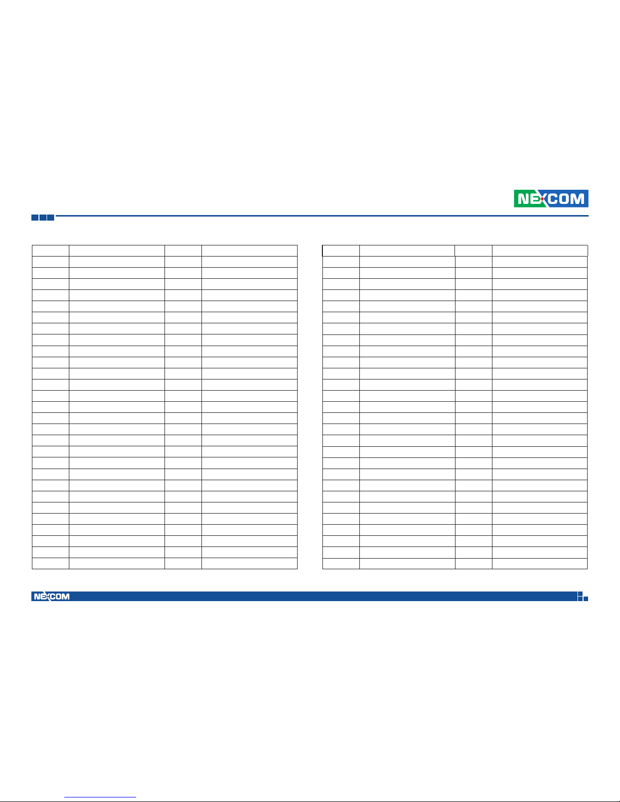
COM Express Connector
MH1
MH2
Row A
Pin Definition Pin Definition
A1 GND A2 GBE0_MDI3A3 GBE0_MDI3+ A4 NC
A5 NC A6 GBE0_MDI2A7 GBE0_MDI2+ A8 GBE0_LINK#
A9 GBE0_MDI1- A10 GBE0_MDI1+
A11 GND A12 GBE0_MDI0A13 GBE0_MDI0+ A14 GBE0_CTREF
Row B
Pin Definition Pin Definition
B1 GND B2 GBE0_ACT#
B3 LPC_FRAME# B4 LPC_AD0
B5 LPC_AD1 B6 LPC_AD2
B7 LPC_AD3 B8 NC
B9 NC B10 LPC_CLK
B11 GND B12 PWRBTN#
B13 SMB_CK B14 SMB_DAT
Page 49
Copyright © 2012 NEXCOM International Co., Ltd. All Rights Reserved.
35
Chapter 3: Jumpers and Switches
VTC 7120-BK Series User Manual
Pin Definition Pin Definition
A15 SUS_S3# A16 SATA0_TX+
A17 SATA0_TX- A18 SUS_S4#
A19 SATA0_RX+ A20 SATA0_RXA21 GND A22 NC
A23 NC A24 SUS_S5#
A25 NC A26 NC
A27 BATLOW# A28 ATA_ACT#
A29 AC_SYNC A30 AC_RST#
A31 GND A32 AC_BITCLK
A33 AC_SDOUT A34 NC
A35 NC A36 USB6A37 USB6+ A38 USB_6_7_OC#
A39 USB4- A40 USB4+
A41 GND A42 USB2A43 USB2+ A44 USB_2_3_OC#
A45 USB0- A46 USB0+
A47 VCC_RTC A48 NC
A49 NC A50 NC
A51 GND A52 NC
A53 NC A54 NC
A55 NC A56 NC
A57 GND A58 NC
A59 NC A60 GND
A61 NC A62 NC
A63 GPI1 A64 NC
A65 NC A66 GND
A67 NC A68 PCIE_TX0+
A69 PCIE_TX0- A70 GND
Pin Definition Pin Definition
B15 SMB_ALERT# B16 NC
B17 NC B18 SUS_STAT#
B19 NC B20 NC
B21 GND B22 NC
B23 NC B24 PWR_OK
B25 NC B26 NC
B27 NC B28 NC
B29 NC B30 AC_SDIN0
B31 GND B32 SPKR
B33 I2C_CK B34 I2C_DAT
B35 THRM# B36 NC
B37 NC B38 USB_4_5_OC#
B39 USB5- B40 USB5+
B41 GND B42 USB3B43 USB3+ B44 USB_0_1_OC#
B45 USB1- B46 USB1+
B47 NC B48 NC
B49 SYS_RESET# B50 CB_RESET#
B51 GND B52 NC
B53 NC B54 NC
B55 NC B56 NC
B57 NC B58 NC
B59 NC B60 GND
B61 NC B62 NC
B63 GPO3 B64 NC
B65 NC B66 NC
B67 NC B68 PCIE_RX0+
B69 PCIE_RX0- B70 GND
Page 50
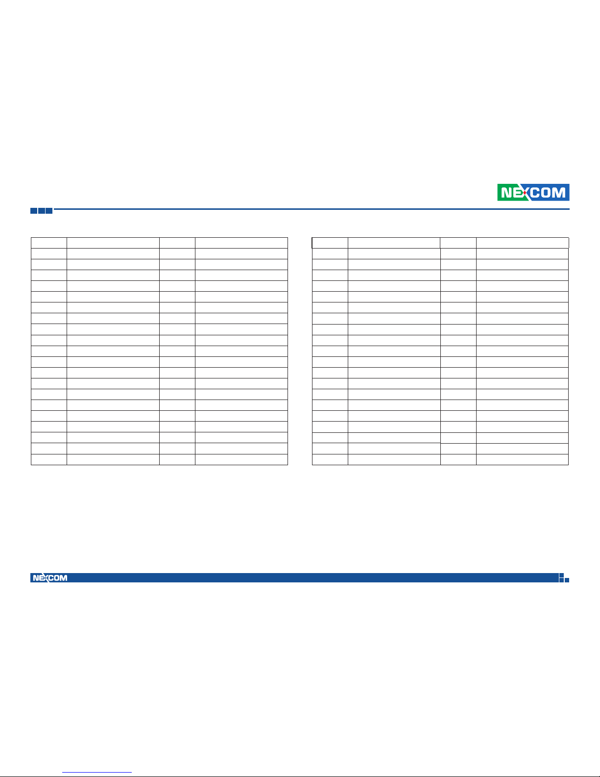
Copyright © 2012 NEXCOM International Co., Ltd. All Rights Reserved.
36
Chapter 3: Jumpers and Switches
VTC 7120-BK Series User Manual
Pin Definition Pin Definition
A71 LVDS_A0+ A72 LVDS_A0A73 LVDS_A1+ A74 LVDS_A1+
A75 LVDS_A2+ A76 LVDS_A2+
A77 LVDS_VDD_EN A78 LVDS_A3+
A79 LVDS_A3+ A80 GND
A81 LVDS_A_CK+ A82 LVDS_A_CKA83 LVDS_I2C_CK A84 LVDS_I2C_DAT
A85 NC A86 NC
A87 NC A88 PCIE0_CK_REF+
A89 PCIE0_CK_REF- A90 GND
A91 RSVD A92 RSVD
A93 NC A94 RSVD
A95 RSVD A96 GND
A97 VCC_12V A98 VCC_12V
A99 VCC_12V A100 GND
A101 VCC_12V A102 VCC_12V
A103 VCC_12V A104 VCC_12V
A105 VCC_12V A106 VCC_12V
A107 VCC_12V A108 VCC_12V
A109 VCC_12V A110 GND
Pin Definition Pin Definition
B71 NC B72 NC
B73 NC B74 NC
B75 NC B76 NC
B77 NC B78 NC
B79 LVDS_BKLT_EN B80 GND
B81 NC B82 NC
B83 LVDS_BKLT_CTRL B84 VCC_5V_SBY
B85 VCC_5V_SBY B86 VCC_5V_SBY
B87 VCC_5V_SBY B88 RSVD
B89 NC B90 GND
B91 NC B92 NC
B93 NC B94 NC
B95 NC B96 NC
B97 NC B98 NC
B99 NC B100 GND
B101 VCC_12V B102 VCC_12V
B103 VCC_12V B104 VCC_12V
B105 VCC_12V B106 VCC_12V
B107 VCC_12V B108 VCC_12V
B109 VCC_12V B110 GND
Page 51
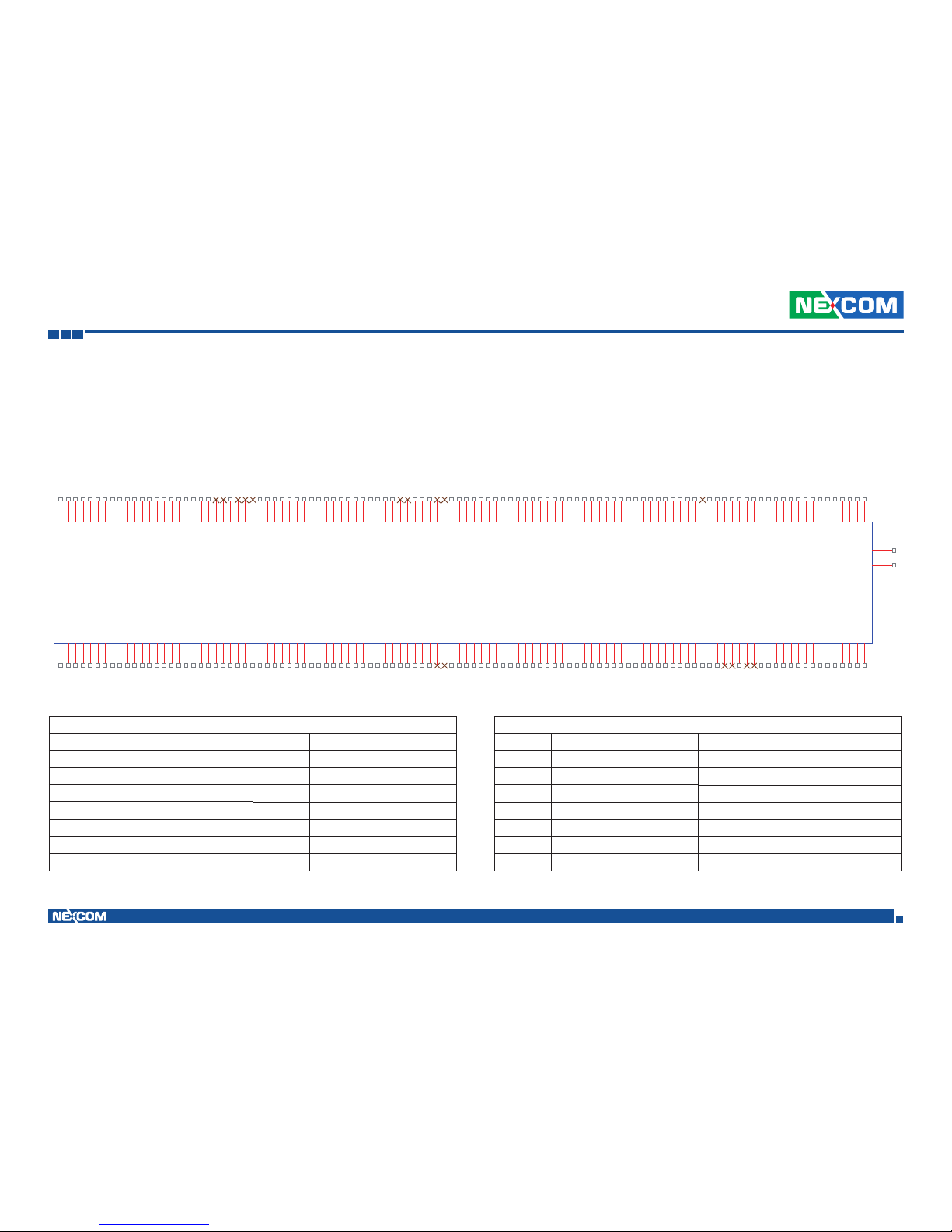
Copyright © 2012 NEXCOM International Co., Ltd. All Rights Reserved.
37
Chapter 3: Jumpers and Switches
VTC 7120-BK Series User Manual
High Speed Board-to-Board Connector: COM
Express Row C and Row D
Connector size: 2 X 110 = 220 Pin
Connector location: J12B
A1A2A3A4A5A6A7A8A9
A10
A11
A12
A13
A14
A15
A16
A17
A18
A19
A20
A21
A22
A23
A24
A25
A26
A27
A28
A29
A30
A31
A32
A33
A34
A35
A36
A37
A38
A39
A40
A41
A42
A43
A44
A45
A46
A47
A48
A49
A50
A51
A52
A53
A54
A55
A56
A57
A58
A59
A60
A61
A62
A63
A64
A65
A66
A67
A68
A69
A70
A71
A72
A73
A74
A75
A76
A77
A78
A79
A80
A81
A82
A83
A84
A85
A86
A87
A88
A89
A90
A91
A92
A93
A94
A95
A96
A97
A98
A99
A100
A101
A102
A103
A104
A105
A106
A107
A108
A109
A110
B1B2B3B4B5B6B7B8B9
B10
B11
B12
B13
B14
B15
B16
B17
B18
B19
B20
B21
B22
B23
B24
B25
B26
B27
B28
B29
B30
B31
B32
B33
B34
B35
B36
B37
B38
B39
B40
B41
B42
B43
B44
B45
B46
B47
B48
B49
B50
B51
B52
B53
B54
B55
B56
B57
B58
B59
B60
B61
B62
B63
B64
B65
B66
B67
B68
B69
B70
B71
B72
B73
B74
B75
B76
B77
B78
B79
B80
B81
B82
B83
B84
B85
B86
B87
B88
B89
B90
B91
B92
B93
B94
B95
B96
B97
B98
B99
B100
B101
B102
B103
B104
B105
B106
B107
B108
B109
B110
MH1
A1A2A3A4A5A6A7A8A9
A10
A11
A12
A13
A14
A15
A16
A17
A18
A19
A20
A21
A22
A23
A24
A25
A26
A27
A28
A29
A30
A31
A32
A33
A34
A35
A36
A37
A38
A39
A40
A41
A42
A43
A44
A45
A46
A47
A48
A49
A50
A51
A52
A53
A54
A55
A56
A57
A58
A59
A60
A61
A62
A63
A64
A65
A66
A67
A68
A69
A70
A71
A72
A73
A74
A75
A76
A77
A78
A79
A80
A81
A82
A83
A84
A85
A86
A87
A88
A89
A90
A91
A92
A93
A94
A95
A96
A97
A98
A99
A100
A101
A102
A103
A104
A105
A106
A107
A108
A109
A110
B1B2B3B4B5B6B7B8B9
B10
B11
B12
B13
B14
B15
B16
B17
B18
B19
B20
B21
B22
B23
B24
B2
5
B26
B27
B28
B29
B30
B31
B32
B33
B34
B35
B36
B37
B38
B39
B40
B41
B42
B43
B44
B45
B46
B47
B48
B49
B50
B51
B52
B53
B54
B55
B56
B57
B58
B59
B60
B61
B62
B63
B64
B65
B66
B67
B68
B69
B70
B71
B72
B73
B74
B75
B76
B77
B78
B79
B80
B81
B82
B83
B84
B85
B86
B87
B88
B89
B90
B91
B92
B93
B94
B95
B96
B97
B98
B99
B100
B101
B102
B103
B104
B105
B106
B107
B108
B109
B110
MH1
MH2
MH2
Row D
Row C
COM Express Connector
Row C
Pin Definition Pin Definition
C1 GND C2 IDE_D7
C3 IDE_D6 C4 IDE_D3
C5 IDE_D15 C6 IDE_D8
C7 IDE_D9 C8 IDE_D2
C9 IDE_D13 C10 IDE_D1
C11 GND C12 IDE_D14
C13 IDE_IORDY C14 IDE_IOR#
Row D
Pin Definition Pin Definition
D1 GND D2 IDE_D5
D3 IDE_D10 D4 IDE_D11
D5 IDE_D12 D6 IDE_D4
D7 IDE_D0 D8 IDE_REQ
D9 IDE_IOW# D10 IDE_ACK#
D11 GND D12 IDE_IRQ
D13 IDE_A0 D14 IDE_A1
Page 52
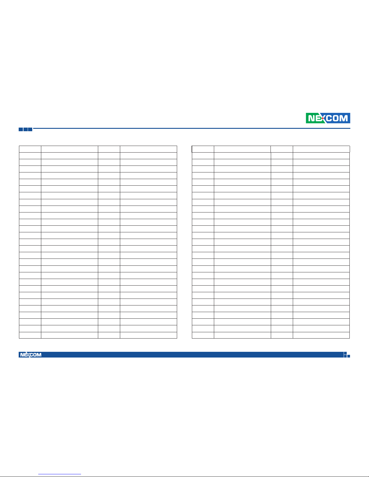
Copyright © 2012 NEXCOM International Co., Ltd. All Rights Reserved.
38
Chapter 3: Jumpers and Switches
VTC 7120-BK Series User Manual
Pin Definition Pin Definition
C15 NC C16 NC
C17 NC C18 NC
C19 NC C20 PCI_GNT0#
C21 GND C22 PCI_REQ0#
C23 PCI_RESET# C24 PCI_AD0
C25 PCI_AD2 C26 PCI_AD4
C27 PCI_AD6 C28 PCI_AD8
C29 PCI_AD10 C30 PCI_AD12
C31 GND C32 PCI_AD14
C33 PCI_C/BE1# C34 PCI_PERR#
C35 PCI_LOCK# C36 PCI_DEVSEL#
C37 PCI_IRDY# C38 PCI_C/BE2#
C39 PCI_AD17 C40 PCI_AD19
C41 GND C42 PCI_AD21
C43 PCI_AD23 C44 PCI_C/BE3#
C45 PCI_AD25 C46 PCI_AD27
C47 PCI_AD29 C48 PCI_AD31
C49 PCI_IRQA# C50 PCI_IRQB#
C51 GND C52 PEG_RX0+
C53 PEG_RX0- C54 NC
C55 NC C56 NC
C57 NC C58 NC
C59 NC C60 GND
C61 NC C62 NC
C63 NC C64 NC
C65 NC C66 NC
C67 NC C68 NC
C69 NC C70 GND
Pin Definition Pin Definition
D15 IDE_A2 D16 IDE_CS1#
D17 IDE_CS3# D18 IDE_RESET#
D19 NC D20 NC
D21 GND D22 PCI_AD1
D23 PCI_AD3 D24 PCI_AD5
D25 PCI_AD7 D26 PCI_C/BE0#
D27 PCI_AD9 D28 PCI_AD11
D29 PCI_AD13 D30 PCI_AD15
D31 GND D32 PCI_PAR
D33 PCI_SERR# D34 PCI_STOP#
D35 PCI_TRDY# D36 PCI_FRAME#
D37 PCI_AD16 D38 PCI_AD18
D39 PCI_AD20 D40 PCI_AD22
D41 GND D42 PCI_AD24
D43 PCI_AD26 D44 PCI_AD28
D45 PCI_AD30 D46 PCI_IRQC#
D47 PCI_IRQD# D48 PCI_CLKRUN#
D49 PCI_M66EN D50 PCI_CLK
D51 GND D52 SDVOB_RED+
D53 SDVOB_RED- D54 PEG_LANE_RV#
D55 SDVOB_GREEN+ D56 SDVOB_GREEND57 NC D58 SDVOB_BLUE+
D59 SDVOB_BLUE- D60 GND
D61 SDVO_CLK+ D62 SDVO_CLKD63 NC D64 NC
D65 NC D66 NC
D67 GND D68 NC
D69 NC D70 GND
Page 53
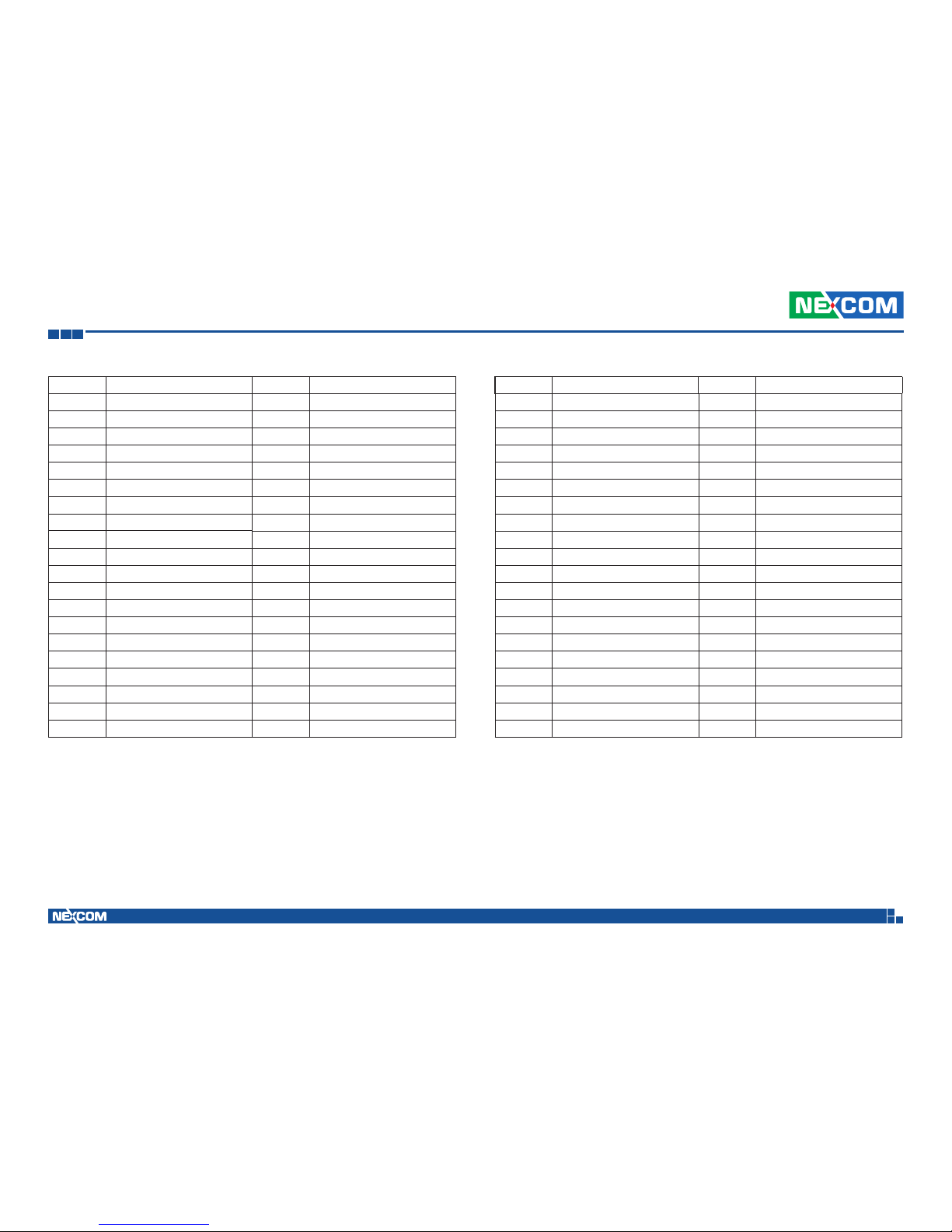
Copyright © 2012 NEXCOM International Co., Ltd. All Rights Reserved.
39
Chapter 3: Jumpers and Switches
VTC 7120-BK Series User Manual
Pin Definition Pin Definition
C71 NC C72 NC
C73 NC C74 NC
C75 NC C76 GND
C77 NC C78 NC
C79 NC C80 GND
C81 NC C82 NC
C83 NC C84 GND
C85 NC C86 NC
C87 GND C88 NC
C89 NC C90 GND
C91 NC C92 NC
C93 GND C94 NC
C95 NC C96 GND
C97 NC C98 NC
C99 NC C100 GND
C101 NC C102 NC C103 GND C104 VCC_12V
C105 VCC_12V C106 VCC_12V
C107 VCC_12V C108 VCC_12V
C109 VCC_12V C110 GND
Pin Definition Pin Definition
D71 NC D72 NC
D73 SDVO_CLK D74 NC
D75 NC D76 GND
D77 IDE_CBLID# D78 NC
D79 NC D80 GND
D81 NC D82 NC
D83 NC D84 GND
D85 NC D86 NC
D87 GND D88 NC
D89 NC D90 GND
D91 NC D92 NC
D93 GND D94 NC
D95 NC D96 GND
D97 PEG_ENABLE# D98 NC
D99 NC D100 GND
D101 NC D102 NC
D103 GND D104 VCC_12V
D105 VCC_12V D106 VCC_12V
D107 VCC_12V D108 VCC_12V
D109 VCC_12V D110 GND
Page 54
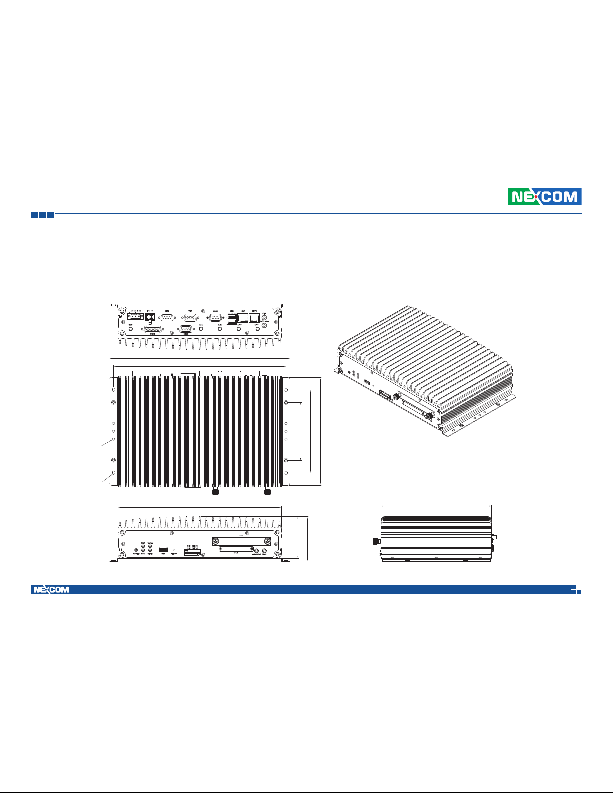
Copyright © 2012 NEXCOM International Co., Ltd. All Rights Reserved.
40
Chapter 4: Mechanical Dimensions
VTC 7120-BK Series User Manual
Chapter 4: Mechanical Dimensions
VTC 7120-BK
286.40
274.40
Ø4
Ø4
92.00
132.00
172.00
72.50
66.50
260.00
260.00
Page 55
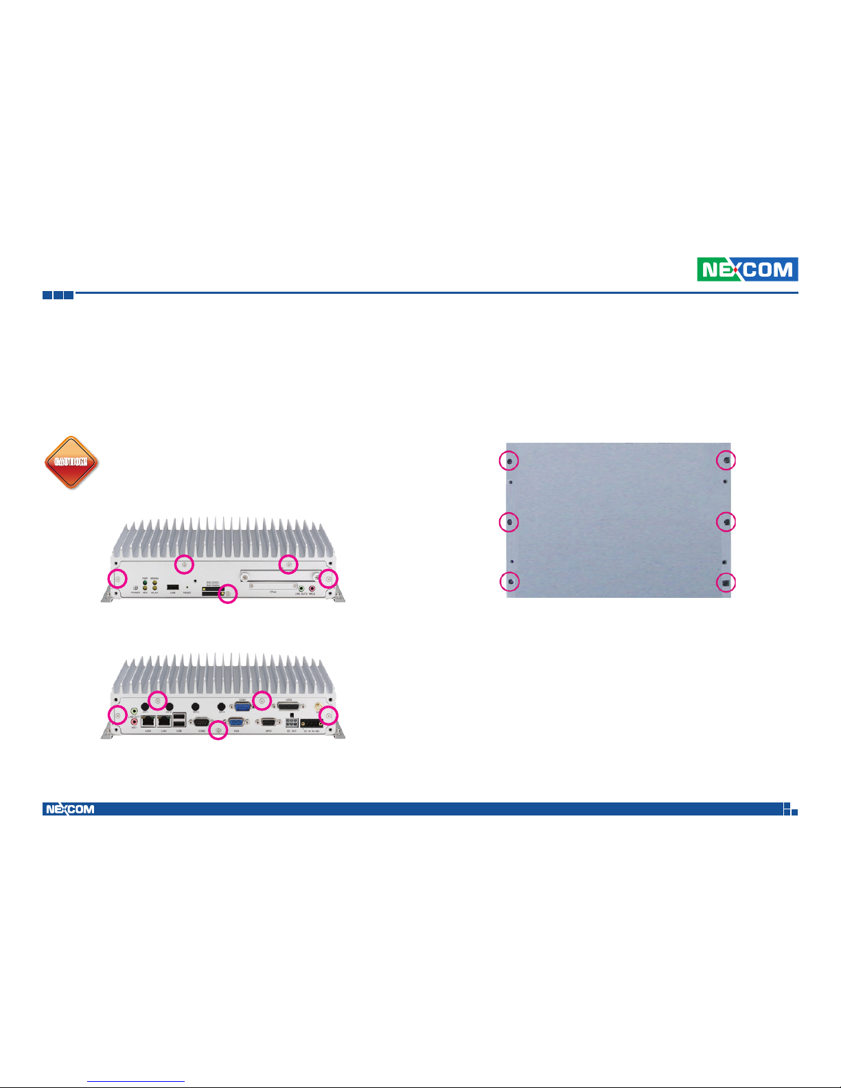
Copyright © 2012 NEXCOM International Co., Ltd. All Rights Reserved.
41
Chapter 5: System Setup
VTC 7120-BK Series User Manual
Chapter 5: System Setup
Bottom View
Removing the Chassis Cover
Prior to removing the chassis cover, make sure the unit’s power
is off and disconnected from the power sources to prevent
electric shock or system damage.
CAUTION!
CAUTION!CAUTION!
Front View
Rear View
Page 56
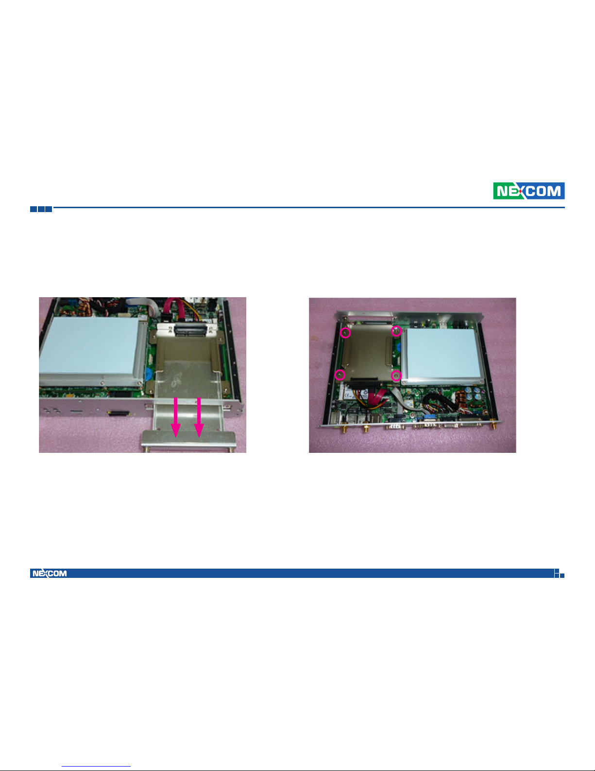
Copyright © 2012 NEXCOM International Co., Ltd. All Rights Reserved.
42
Chapter 5: System Setup
VTC 7120-BK Series User Manual
Installing a GPRS/UMTS/HSDPA Module
1. When you want to install the Mini PCI Express card, you have to remove
the SSD tray and bracket.
First, remove the SSD tray.
2. Remove the SSD bracket.
Page 57
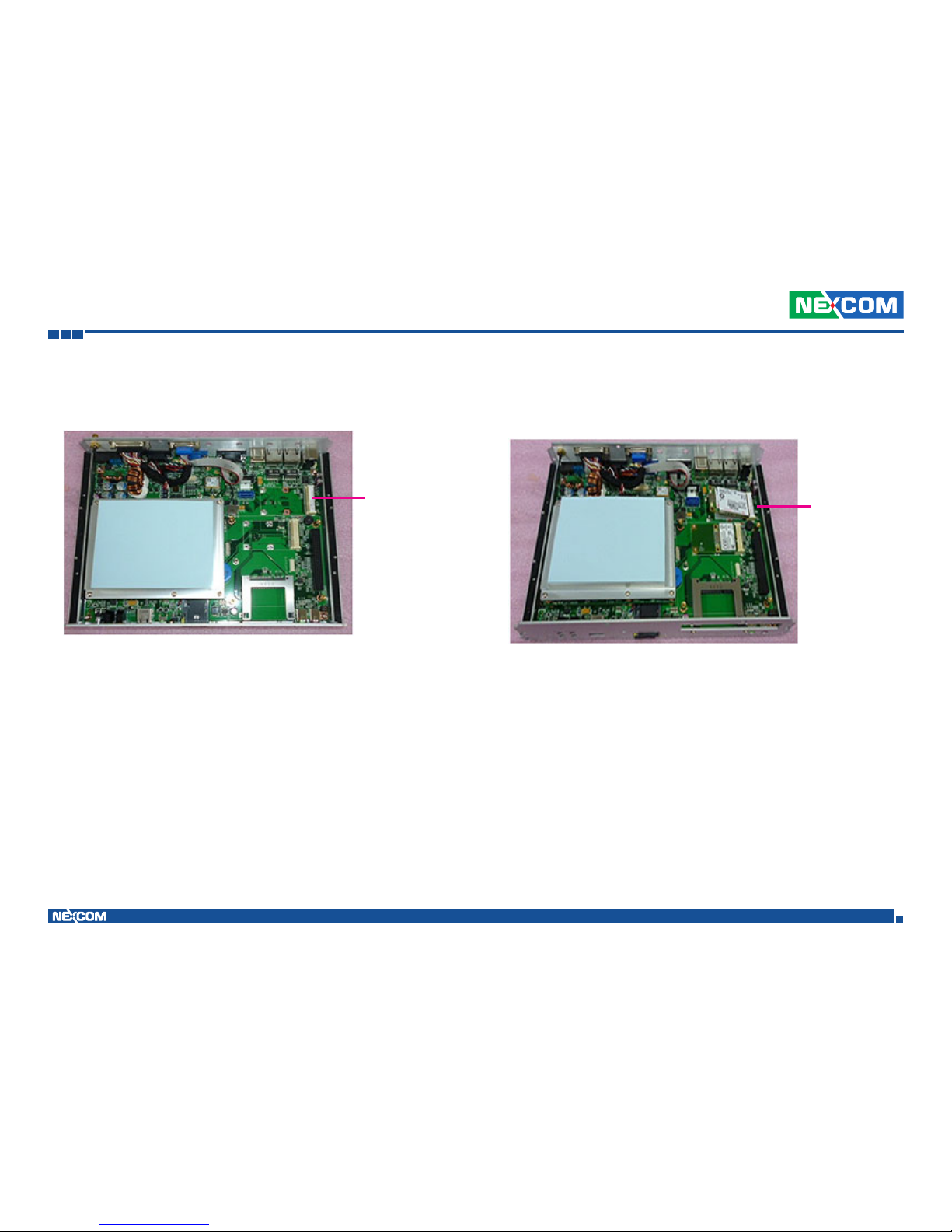
Copyright © 2012 NEXCOM International Co., Ltd. All Rights Reserved.
43
Chapter 5: System Setup
VTC 7120-BK Series User Manual
4. Insert the module into the Mini PCI Express slot at a 45 degrees angle
until the gold-plated connector on the edge of the module completely
disappears inside the slot.
GPRS/UMTS/
HSDPA module
3. The Mini PCI Express slot shown below is used to install a 3.5G
communication module such as GPRS, UMTS or HSDPA module.
Mini PCI
Express slot
Page 58
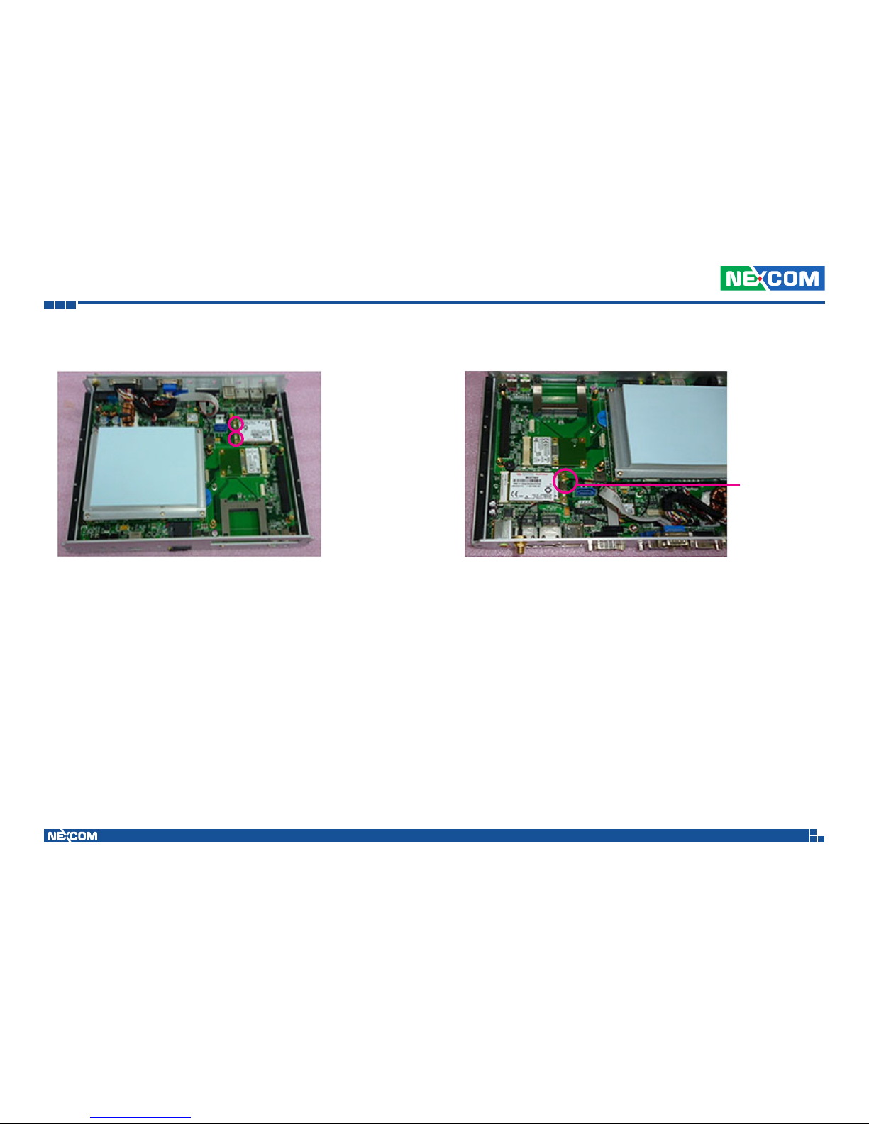
Copyright © 2012 NEXCOM International Co., Ltd. All Rights Reserved.
44
Chapter 5: System Setup
VTC 7120-BK Series User Manual
6. Attach one end of the RF cable onto the module.
Attach RF cable
to the modul
5. Push the module down then secure it with mounting screws.
Page 59
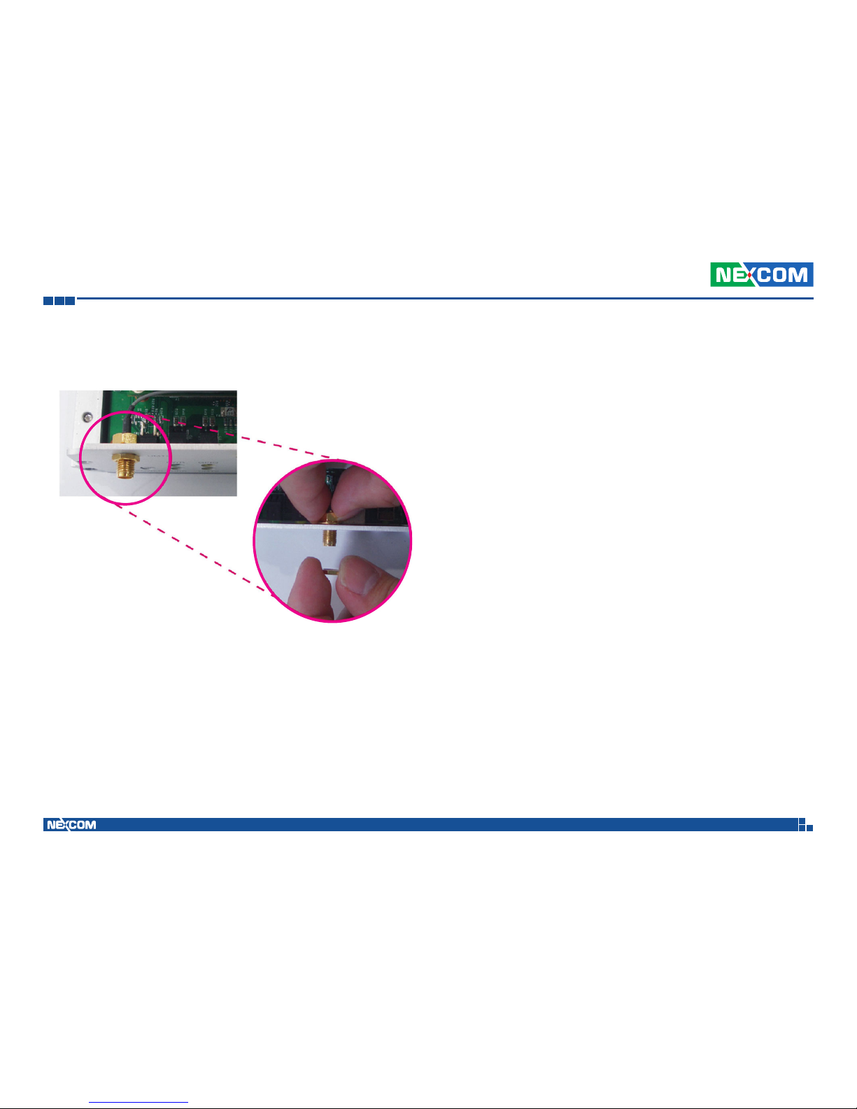
Copyright © 2012 NEXCOM International Co., Ltd. All Rights Reserved.
45
Chapter 5: System Setup
VTC 7120-BK Series User Manual
7. Mount the other end of the cable to the antenna mounting hole located
at the front panel of the chassis.
Page 60
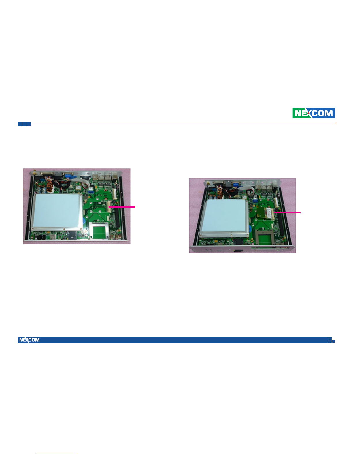
Copyright © 2012 NEXCOM International Co., Ltd. All Rights Reserved.
46
Chapter 5: System Setup
VTC 7120-BK Series User Manual
Installing a Wireless LAN Module
1. The Mini PCI Express slot shown below is used to install a wireless LAN
module.
Mini PCI
Express slot
2. Insert the wireless LAN module into the Mini PCI Express slot at a 45
degrees angle until the gold-plated connector on the edge of the
module completely disappears inside the slot.
Wireless LAN
module
Page 61
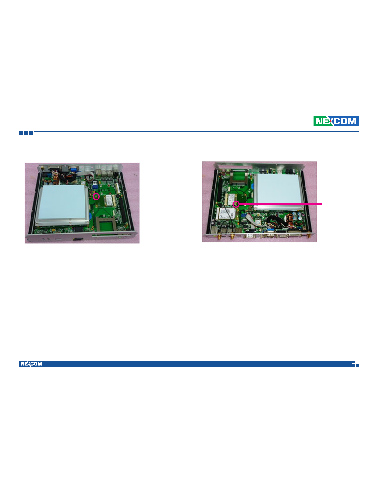
Copyright © 2012 NEXCOM International Co., Ltd. All Rights Reserved.
47
Chapter 5: System Setup
VTC 7120-BK Series User Manual
3. Push the module down then secure it with mounting screws. 4. Attach one end of the RF cable onto the module.
Attach RF cable
to the module
Page 62
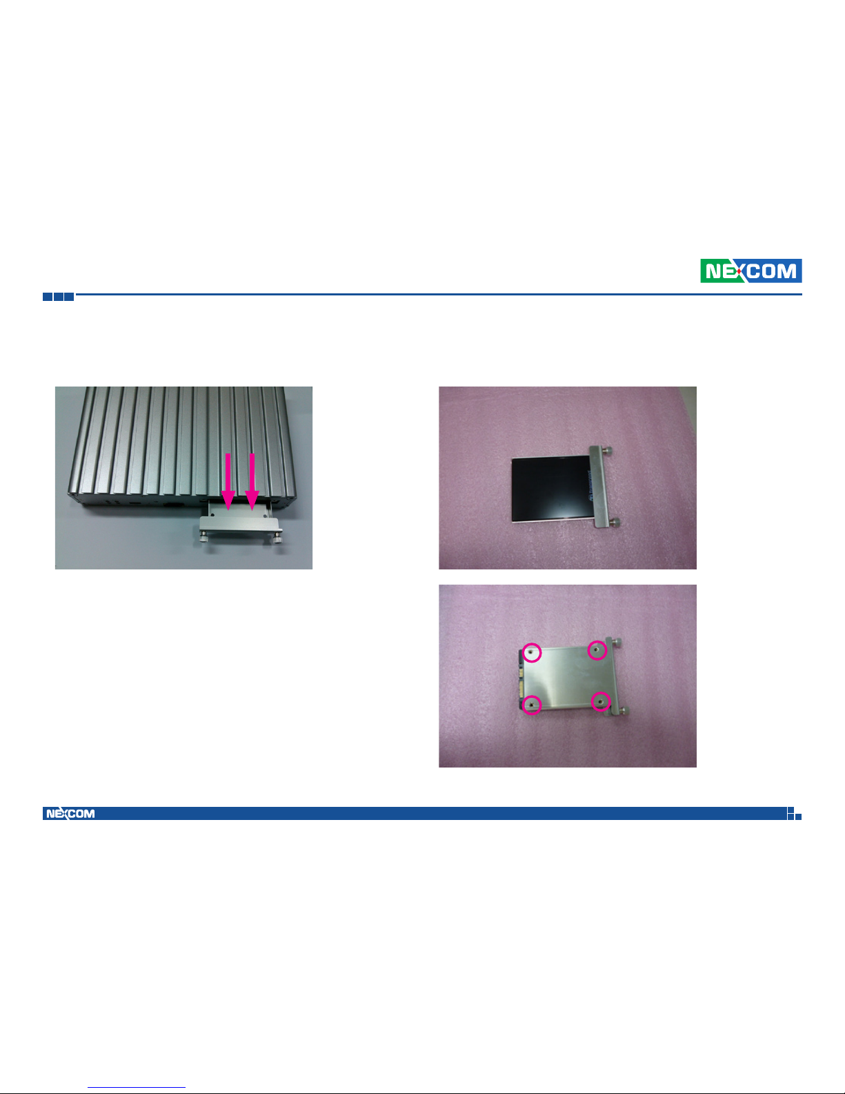
Copyright © 2012 NEXCOM International Co., Ltd. All Rights Reserved.
48
Chapter 5: System Setup
VTC 7120-BK Series User Manual
Installing a SATA SSD Drive
1. Remove the SSD tray.
2. Place the SDD drive into the tray and then tighten the four screws.
Page 63
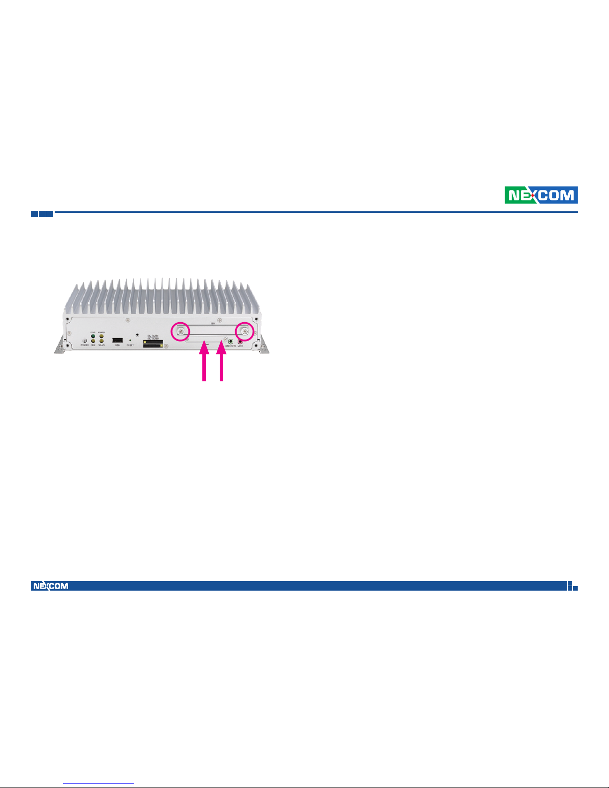
Copyright © 2012 NEXCOM International Co., Ltd. All Rights Reserved.
49
Chapter 5: System Setup
VTC 7120-BK Series User Manual
3. Install the HDD tray, and then tighten the screws to secure the drive to
the chassis.
Page 64
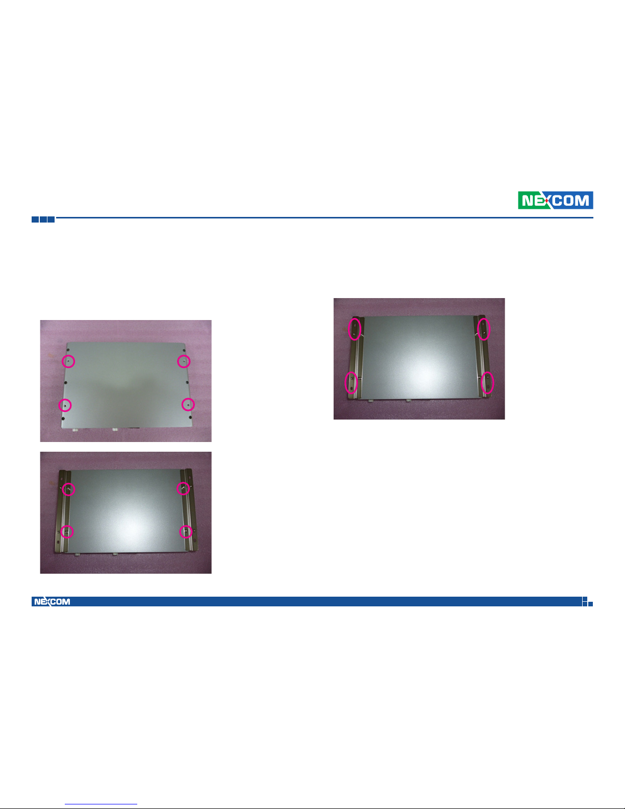
Copyright © 2012 NEXCOM International Co., Ltd. All Rights Reserved.
50
Chapter 5: System Setup
VTC 7120-BK Series User Manual
Rackmount Brackets
The rackmount brackets provide a convenient and economical way of
mounting the system on the wall.
1. The mounting holes are located at the bottom of the system. Secure the
brackets on each side of the system using the provided mounting screws.
2. Now mount the system on the wall by fastening screws through the
bracket’s mounting holes.
Page 65

Copyright © 2012 NEXCOM International Co., Ltd. All Rights Reserved.
51
Chapter 6: Driver Installation
VTC 7120-BK Series User Manual
Chapter 6: Driver Installation
When you want to install the VTC 7120-BK series driver, please refer to the
following steps, it will help you with the driver installation.
Note: Please change the path according to the product name.
Step 1. Installing the Intel® Chipset driver
Please access the folder: \\VTC7110\Chipset Driver
After successful installation, please restart the VTC
Step 2. Installing the Graphic driver
Please access the folder: \\VTC7110\Graphic Driver
After successful installation, please restart the VTC
Step 3. Installing the ME driver
Please access the folder: \\VTC7110\ME Driver
Step 4. Installing the LAN driver
Please access the folder: \\VTC7110\LAN Driver
Step 5. Installing the Audio driver
Please access the folder: \\VTC7110\Audio Driver
After successful installation, please restart the VTC
Step 6. Installing the WLAN module driver
Please access the folder: \\VTC7110\Module Driver\WLAN Module\
Step 7. Installing the WWAN module driver
Please access the folder: \\VTC7110\Module Driver\WWAN Module\
Page 66
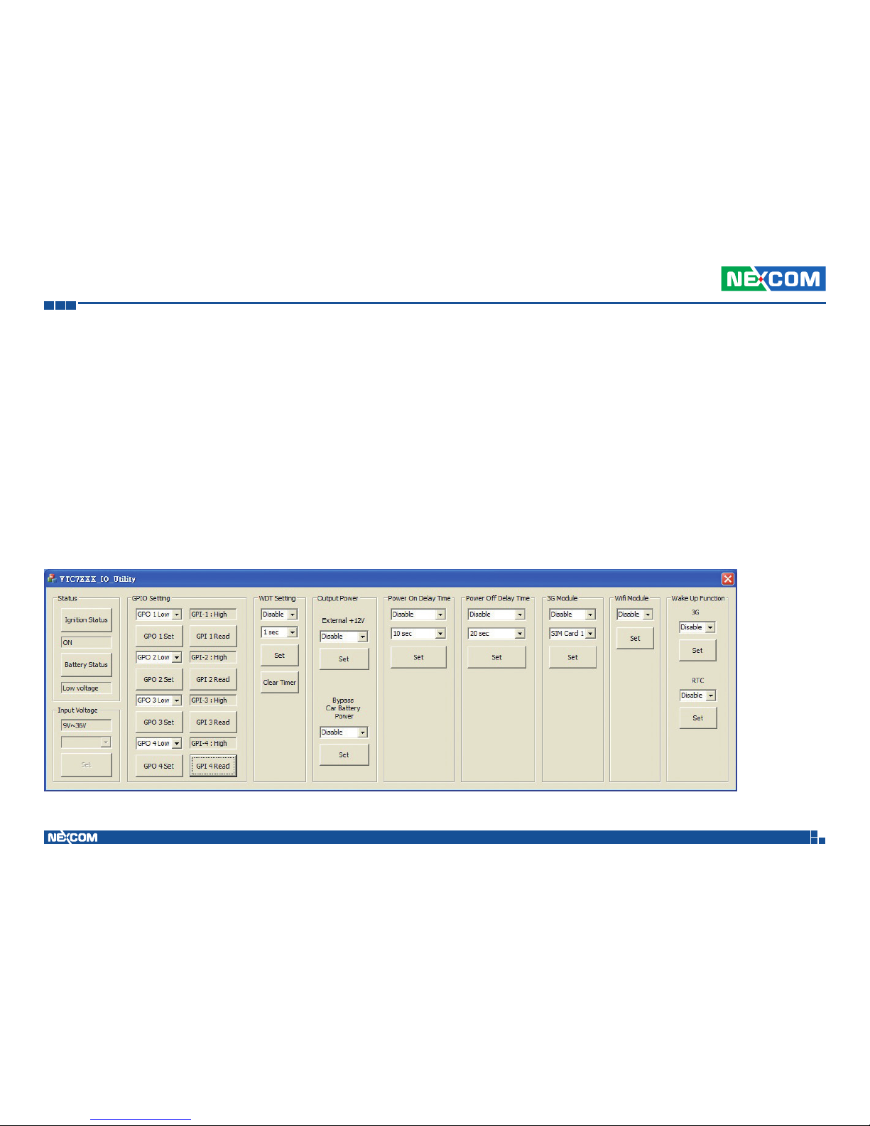
Copyright © 2012 NEXCOM International Co., Ltd. All Rights Reserved.
52
Appendix A: Software Demo Utility for I/O Ports of Function Control
VTC 7120-BK Series User Manual
Appendix A:
Software Demo Utility for I/O Ports of Function Control
NEXCOM’s software demo utility enables users to test and control different
I/O port functions on the VTC 7120-BK. This document shows how to use
the utility.
There are also source code files of the utility in the CD. Users can refer to the
source codes to develop their applications.
Menu Screen
Page 67
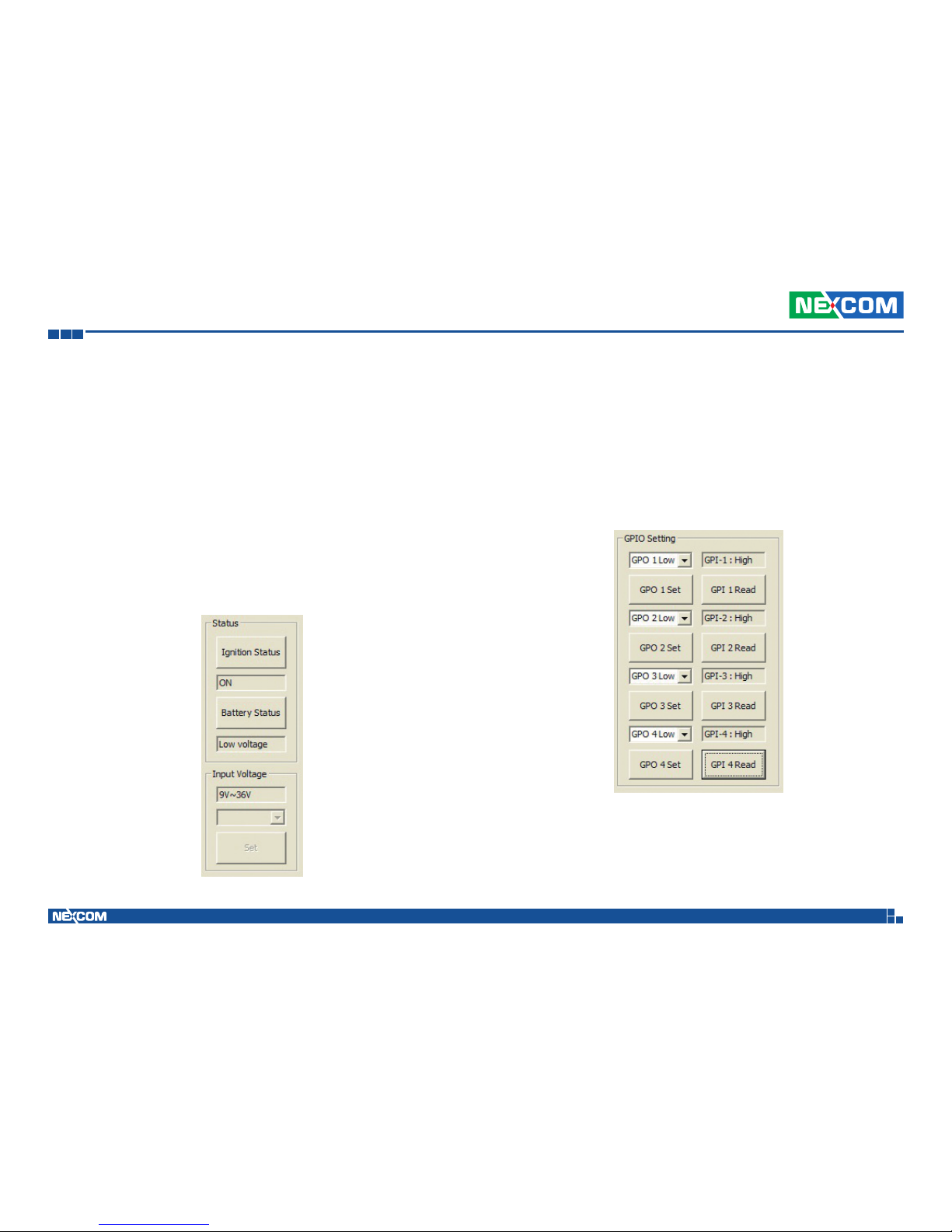
Copyright © 2012 NEXCOM International Co., Ltd. All Rights Reserved.
53
Appendix A: Software Demo Utility for I/O Ports of Function Control
VTC 7120-BK Series User Manual
1.1 Status
1.1.1 Ignition Status
Press the button of Ignition Status, the signal of ignition will be shown.
ON …… Signal of ignition is high.
OFF ….. Signal of ignition is low.
1.2 GPIO
1.2.1 GPO Setting
Press the button of Ignition Status, the signal of ignition will be shown.
ON …… Signal of ignition is high.
OFF ….. Signal of ignition is low.
1.2.2 GPI Reading
Reads the status of GPI.
1.1.2 Battery Status
Press the button of Battery Status, the status of battery voltage will be shown.
Low voltage …… Signal of ignition is high.
OFF .......…......... Signal of ignition is low.
1.1.3 Input Voltage
Shows the setting of input voltage in BIOS.
Page 68
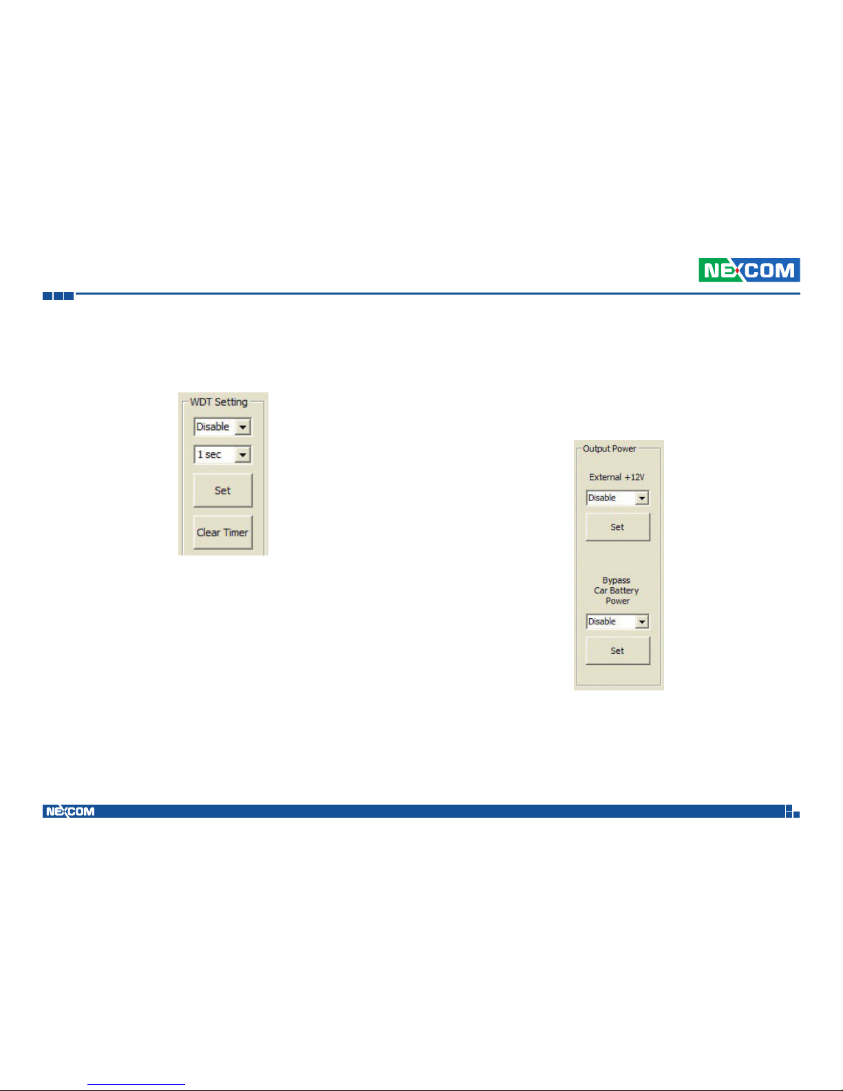
Copyright © 2012 NEXCOM International Co., Ltd. All Rights Reserved.
54
Appendix A: Software Demo Utility for I/O Ports of Function Control
VTC 7120-BK Series User Manual
1.3 WDT Setting
Enables or disables the WDT function. There are 8 selections of time. The
timer of WDT can also be cleared by button.
1.4 Output Power
1.4.1 External +12V
Enables or Disables the output of 12VDC.
1.4.2 Bypass Car Battery Power
Reads the status of GPI.
Page 69
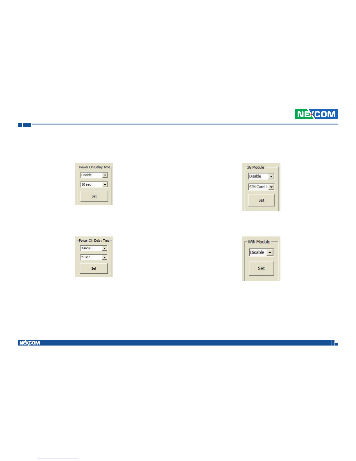
Copyright © 2012 NEXCOM International Co., Ltd. All Rights Reserved.
55
Appendix A: Software Demo Utility for I/O Ports of Function Control
VTC 7120-BK Series User Manual
1.5 Power On Delay Time
Enables or disables the power on delay time function. There are 8 selections
of delay time.
1.6 Power Off Delay Time
Enables or disables the power off delay time function. There are 8 selections
of delay time.
1.7 3G Module
Enables or disables WWAN module function. SIM card 1 or SIM card 2 can
also be selected for the WWAN module on mini-PCIe socket (CN18).
1.8 WLAN Module
Enables or disables WLAN function for the WLAN module on mini-PCIe
socket (CN19).
Page 70
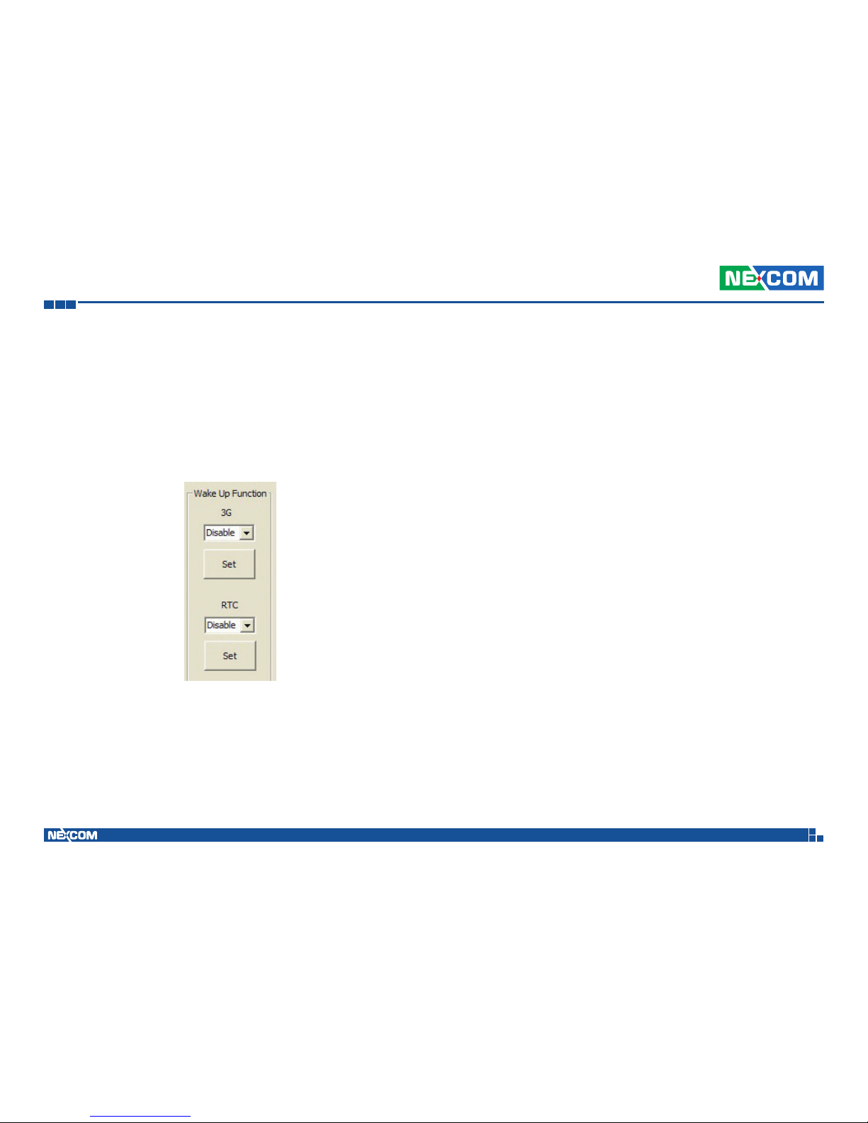
Copyright © 2012 NEXCOM International Co., Ltd. All Rights Reserved.
56
Appendix A: Software Demo Utility for I/O Ports of Function Control
VTC 7120-BK Series User Manual
1.9 Wake Up Function
1.9.1 3G
Enables or disables the wake up function for the WWAN module on
mini-PCIe socket (CN18).
1.9.2 RTC
Enables or disables the RTC wake up function. The timer setting of RTC is
located in BIOS setting.
Page 71
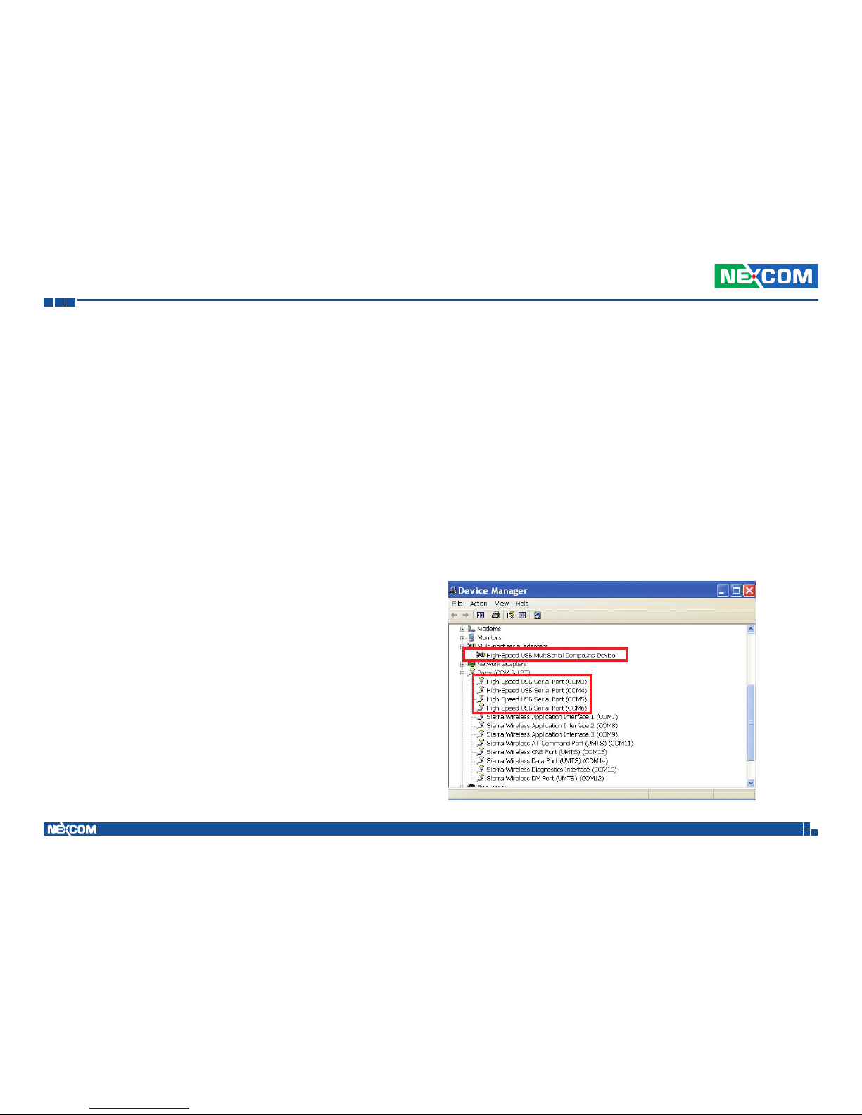
Copyright © 2012 NEXCOM International Co., Ltd. All Rights Reserved.
57
Appendix B: Using the GPS Feature
VTC 7120-BK Series User Manual
Appendix B: Using the GPS Feature
The VTC has a built-in u-blox NEO-6Q GPS receiver module by default.
Global Positioning System (GPS) uses a constellation of 50 medium earth
orbit satellites to transmit and receive microwave signals to determine its
current location.
You need to install the third-party GPS navigation software to take advantage
of the GPS feature.
Setup and Using GPS Information
Users can use the GPSinfo.exe program to verify that the GPS is correctly
configured and working properly. Also, users can use the GPSinfo.exe program to enable WAAS/EGNOS and power saving mode.
1. Go to Device Manager to ensure the device is installed correctly.
u-blox NEO-6Q GPS Module Specification
Receiver Type 50-channel u-blox 6 engine
GPS L1 C/A code
SBAS: WAAS, EGNOS, MSAS
Navigation Update Rate Up to 5 Hz
Accuracy Position: 2.5 m CEP
SBAS: 2.0 m CEP
Acquisition Cold starts: 26s
Aided starts2: 1s
Hot starts: 1s
Sensitivity Tracking: –162 dBm
Cold starts: –148 dBm
Hot starts: –157 dBm
Page 72
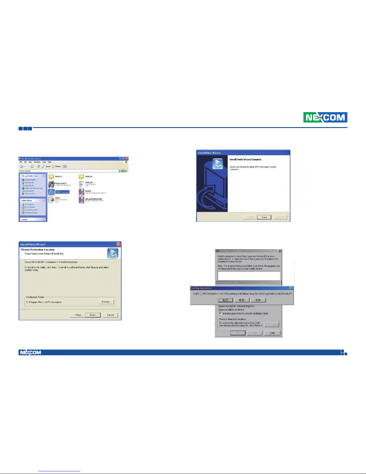
Copyright © 2012 NEXCOM International Co., Ltd. All Rights Reserved.
58
Appendix B: Using the GPS Feature
VTC 7120-BK Series User Manual
2. Insert the Installation Disc into CD-Rom drive and execute the “Gpsinfo.
exe” file (the file also saved in C:\Utility\GPS_Utility).
3. Follow the given instructions to complete the installation.
4. When the setup complete, press <Finish>.
5. Once the installation is completed, installation of GPS Information onto
PDA device will be launched automatically. Select <Yes> to continue.
Page 73
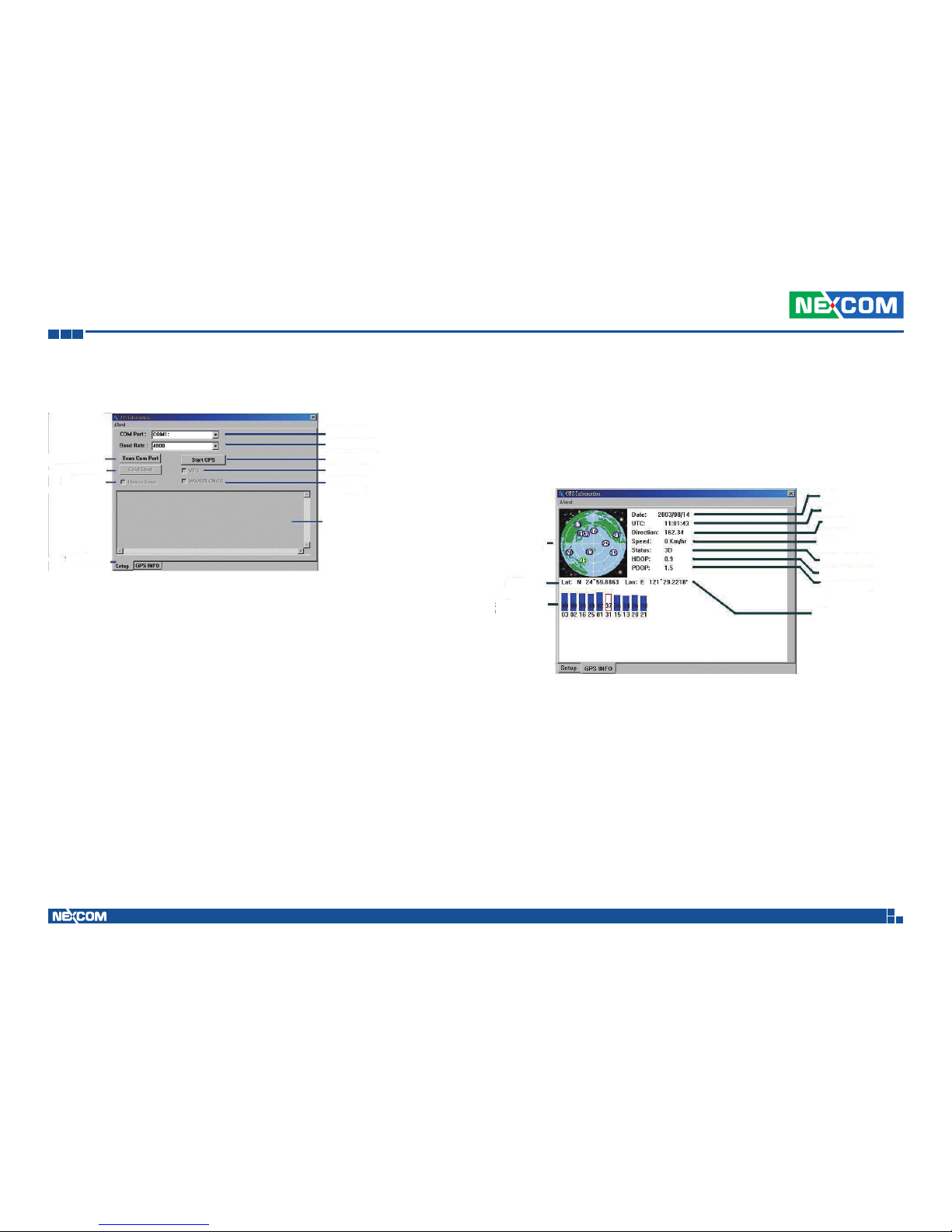
Copyright © 2012 NEXCOM International Co., Ltd. All Rights Reserved.
59
Appendix B: Using the GPS Feature
VTC 7120-BK Series User Manual
Setup Window Screenshot
Double click GpsInfo_Vista icon from Desktop to start GPS.
• Scan Com Port” - Scan all available communication port for GPS recep-
tion
• “Cold Start” - Cold start the GPS receiver
• “Power Save” - Check the box to enable/disable the Power Save Mode
(the option is available only when a GPS device is found)
• “Tab Menu” - Switch between Setup and GPSINFO windows
• “Com Port Selection” - Select the appropriate communication port
where GPS receiver is configured (it may be necessary to try several communication ports until the right one is found)
• “Baud Rate Selection” - Select the appropriate transferring rate (Please
set the baud rate at 38400)
• “Start GPS button” - Turn on/off the GPS device
• “VTG check box” - Some navigation or map software requires to receive
VTG data output for during operation. Check the box to activate the
VTG data output.
Com Port Selection
Baud Rate Selection
Start GPS button
Cold Start
Scan Com Port
Main GPS data
Window
VTG check box
WAAS/EGNOSPower Save
Tab Menu
• “WAAS/EGNOS” - Check the box to activate WAAS/EGNOS in order to
increase the accuracy of positioning
• “Main GPS data Window” - Display data received by GPS device.
GPS Info Window Screenshot
• “Satellite Distribution Map” – Display the position of all connected
Satellites
• A unique number is assigned to each satellite.
• Red circle indicates that the satellite location is known from almanac
information; however, the satellite is not currently being tracked.
• Green circle indicates that the satellite is being tracked; how ever, it is
not being used in the current position solution.
• Blue circle indicates that is being tracked and is being used in the cur-
rent position.
Satellite
Distribution
Map
Latitude
Satellite Status
Chart
Longitude
Position Accuracy
Horizontal Accuracy
Positioning Status
Speed
Direction
Time
Date
Page 74

Copyright © 2012 NEXCOM International Co., Ltd. All Rights Reserved.
60
Appendix B: Using the GPS Feature
VTC 7120-BK Series User Manual
• “Latitude” – User’s current latitude is displayed in N/S degree (North/
South Hemisphere) format
• “Satellite Status Chart” – display the status of each connected satellite
• The number under each bar marks corresponding Satellite, and the
height of each bar represents the strength of the satellite.
• Red bar indicates that the satellite location is known from almanac
information; however, the satellite is not currently being tracked.
• Green solid bar indicates that the satellite is being tracked; however, it
is not being used in the current position solution.
• Blue bar indicates that the tracked and is being used in the current
position.
• “Date” – display the current date in (dd/mm/yy) format.
• “Time” – display the current (UTC) time in (hh:mm:ss) format.
• “Direction” – display the current direction from 000.0° to 359.9°
• “Speed” – Display the current moving speed in km/hour
• “Positioning Status”- Three Modes
1. No Fix
2. 2D Positioning
3. 3D Positioning
• “Horizontal Accuracy” - Range from 0.5 to 99.9, the smaller the better
• “Position Accuracy” - Range from 0.5 to 99.9, the smaller the better
• “Longitude” – Display current longitude in E/W (East/West Hemisphere)
Time (hhmmss)
GPS Information Instructions
1. Make sure that the GPS device is properly inserted.
2. Start GPS Information Software.
3. Choose and select the proper communication port. (It might be neces-
sary to try each available port to find the right one since the default
communication port varies according to different hardware device.)
4. Click “Start GPS button” to activate the GPS receiver.
5. Upon successful connection, GPS output data should be displayed in
“Main GPS data Window”. If no data is observed, make sure the GPS
receiver is working and properly inserted. Otherwise choose another
communication port.
6. Satellite status can be observed in the “GPS Info Window”. Use the
“Tab Menu” to switch between Setup window and GPS info window.
7. Please make sure to de-activate the GPS device before exiting this pro-
gram.
Page 75
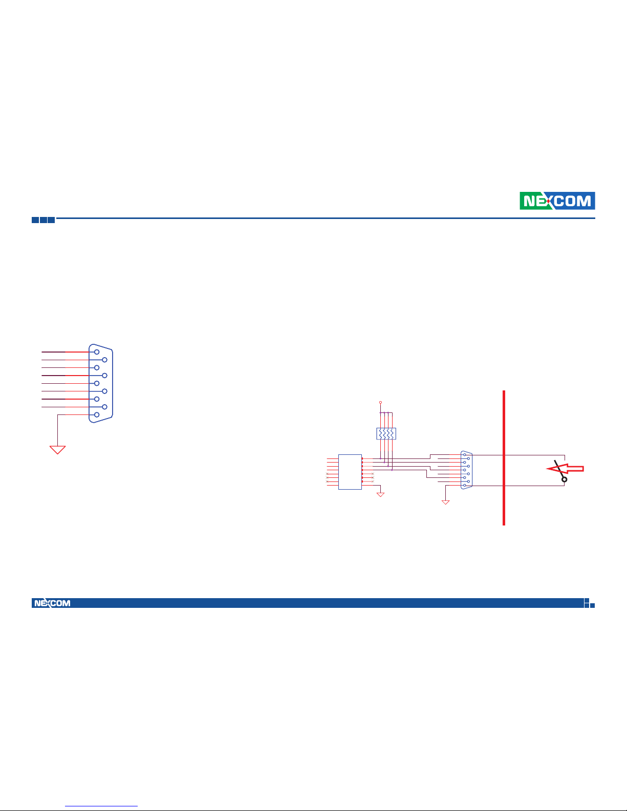
Copyright © 2012 NEXCOM International Co., Ltd. All Rights Reserved.
61
Appendix C: Signal Connection of DI/DO
VTC 7120-BK Series User Manual
The figure below shows how to connect an external output source to one
of the input channel.
Appendix C: Signal Connection of DI/DO
Digital Input
CN18 connector for GPI signal (digital signal input)
The CN18 has 4 digital input channels.
Dry Contact (default)
The GPI signals have a pull up resistor to 5V internally.
G_IN1
G_IN3
G_OUT2
G_OUT4
G_IN2
G_OUT3
G_OUT1
G_IN4
GPIO_GND
CN1
SIO-F-90-5.08mm
CN18
SIO-F-90-5.08mm
5
9
4
8
3
7
2
6
1
ExternalInternal
G_IN4
G_IN1
G_IN2
G_IN3
GPIO_G
VCC5
ND
ULN2003ADRULN2003ADR
1B
1
2B
2
3B
3
4B
4
5B
5
6B
6
7B
7
1C
16
2C
15
3C
14
4C
13
5C
12
6C
11
7C
10
E8COM
9
RN11KRN1
1K
1 8
273
6
4
5
ON==>GND
OFF==>OPEN
GPIO Pinout Description
G_IN1
G_IN3
G_OUT2
G_OUT4
G_IN2
G_OUT3
G_OUT1
G_IN4
GPIO_GND
CN1
SIO-F-90-5.08mm
CN18
SIO-F-90-5.08mm
5
9
4
8
3
7
2
6
1
Wet Contact:
Please contact sales for further information.
Page 76
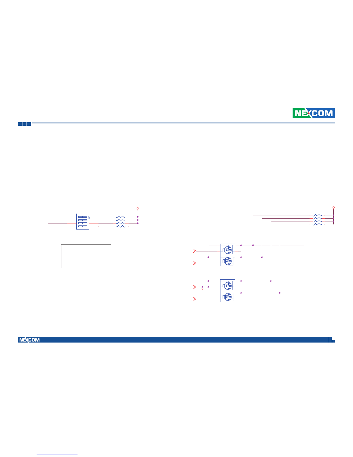
Copyright © 2012 NEXCOM International Co., Ltd. All Rights Reserved.
62
Appendix C: Signal Connection of DI/DO
VTC 7120-BK Series User Manual
Digital Output
CN18 connector for GPO signal (digital signal output)
The CN18 has 4 digital output channels. Each channel can accept 0~30Vdc
voltage. And it is able to drive 250mA current for low level. The signal
connection of CN18 support two connected methods for output signal type.
The output signal has two states, one is low level (driven to 0V from GPO
signal) other is open (high voltage is provided from external device).
G_OUT1
G_OUT2
G_OUT3
G_OUT4
VCC5
330E0603 330E0603
330E0603
Z12003
Z12004
Z12005
Z12006
330E0603
SW4
DIP SW 2X4
SW4
DIP SW 2X4
1
2
3
4
6
5
7
8
330E0603 330E0603
330E0603 330E0603
GPO (SW4)
On Pull up VCC5
Don’t CareO
Wet Contact (default)
The SW4 needs to switch to “ON” state. The GPO signal will have a pull up
resistor to 5V internally when you switch “SW1” to “ON” state. The output
signal has two states, one is low level (driven to 0V from GPO signal ) other
is high level (driven to 5V from GPO signal).
The figure below shows how to connect an external input source to one of
the isolated output channel.
G_OUT1
G_OUT2
G_OUT3
G_OUT4
G_OUT4
G_OUT3
G_OUT2
G_OUT1
VCC5
GPO1
GPO0
GPO2
GPO3
330E0603 330E0603
330E0603 330E0603
EMB17A03GEMB17A03G
8
7
6
5
1
2
3
4
EMB17A03GEMB17A03G
8
7
6
5
1
2
3
4
330E0603 330E0603
330E0603 330E0603
Page 77
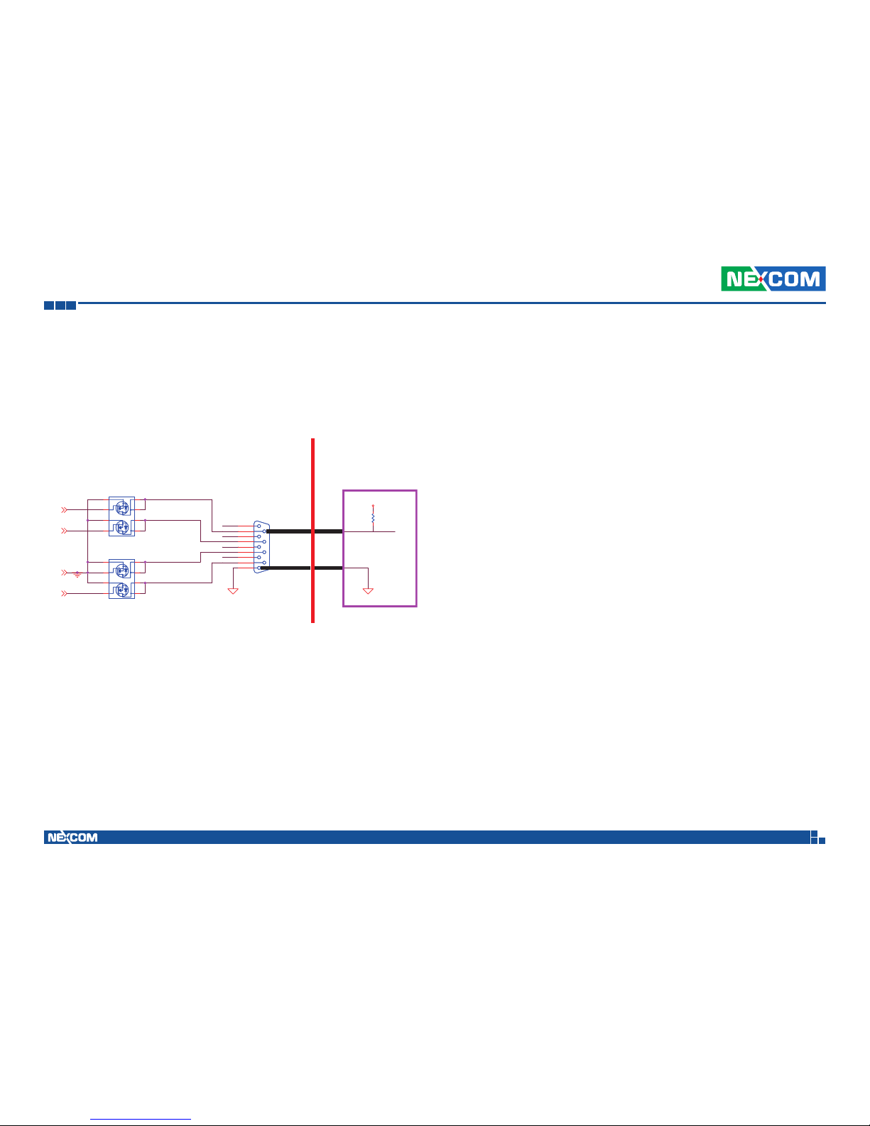
Copyright © 2012 NEXCOM International Co., Ltd. All Rights Reserved.
63
Appendix C: Signal Connection of DI/DO
VTC 7120-BK Series User Manual
The figure below shows how to connect an external input source to one of
the output channel.
G_IN1
G_IN3
G_OUT2
G_OUT4
G_IN2
G_OUT3
G_OUT1
G_IN4
GPIO_GND
GND
CN1
SIO-F-90-5.08mm
CN18
SIO-F-90-5.08mm
5
9
4
8
3
7
2
6
1
ExternalInternal
G_OUT4
G_OUT3
G_OUT2
G_OUT1
GPO1
GPO0
GPO2
GPO3
EMB17A03GEMB17A03G
8
7
6
5
1
2
3
4
EMB17A03GEMB17A03G
8
7
6
5
1
2
3
4
External Device
Input
Resistor
External power
Dry Contact
The SW4 needs to switch to “OFF” state. The GPO signal will no have a pull
up resistor internally when you switch “SW4” to “OFF” state.
Page 78
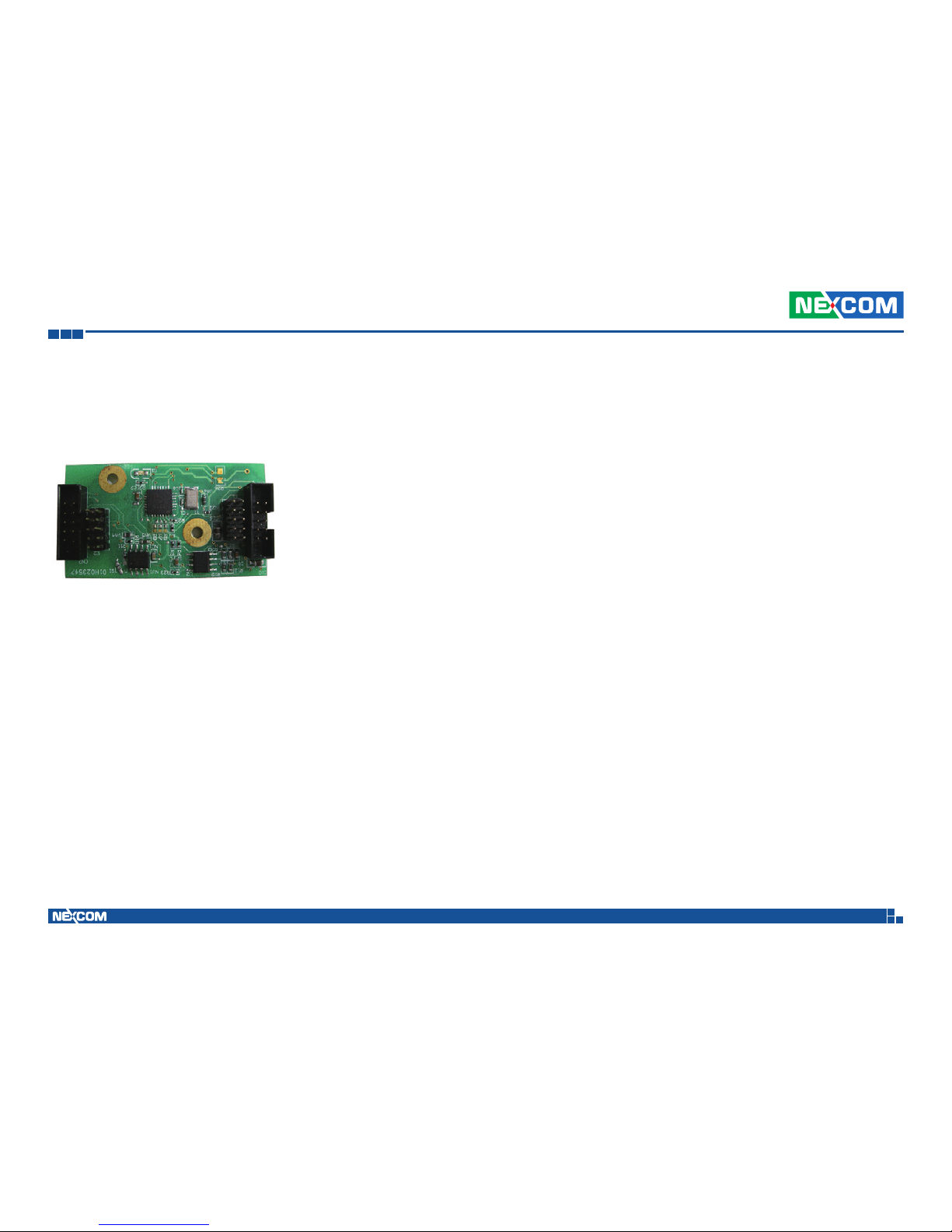
Copyright © 2012 NEXCOM International Co., Ltd. All Rights Reserved.
64
Appendix D: OBDII Module Setup and Command
VTC 7120-BK Series User Manual
Appendix D: OBDII Module Setup and Command
OBDII Module
VTC series offer an option to integrate the OBDII module, VIOX-CAN01, into
VTC system. The form factor of this VIOX-CAN01 is proprietary and it can
support either SAE J1939 or SAE J1708 via connection in the first time. The
maximum VIOX-CAN01 installed in VTC series is up to three units. Please
note they are factory option.
VIOX-CAN01 Setup
When you start connecting VTC device to CAN bus device, you need a
terminal program to send and receive data. To use the terminal program,
please follow the setting below.
(1) Set the proper corresponding “COM” port and its data rate is 9600
(2) Set data bits at 9, stop bit at 1 and no parity bits.
After the setting, you will see the prompt with “>” character. This indicates
that the device is in the idle state and ready to receive characters on the
COM port.
If you do not see prompt string, please reset the device with ATR (reset)
command and then press the return key:
>ATR or >AT R (spaces are optional; and case is in-sensetive).
You can also type HEX code instead:
“41”, “54”, “5A”, “0D”
If you see the strange characters instead of “>”, you may set the incorrect
baud rate. Please check baud rate. If you send the incorrect command, the
device will show a single question mark (“?”) to indicate your input is not
understood. If VTC fails to link to the BUS, it will show “PLEASE REBOOT”.
Once VTC connect to BUS, it will start to try which protocol is connected
either J1939 or J1708. Once it is determined, it will only accept the
successful protocol next time unless using ATR command to reset it. This
means you can change the protocol by reset command. After the reset
command, please power off the device and turn on it again.
In case, the device cannot find correct protocol after 180 seconds, it will
enter sleeping mode for power saving.
There are several output format available for the different application
including:
(1) Simple Data by ASCII Code
(2) Raw Data
(3) Packaged Messages by ASCII or HEX code.
The default setting is Simple Data Format. The device will send messages
out after it communicates with vehicle successfully. The output format can
be changed via setting the AT command. Please refer the following section
of AT command.
Page 79
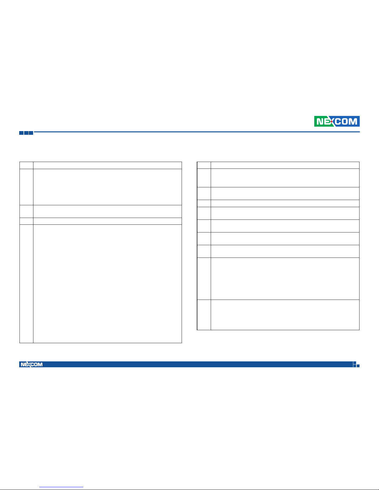
Copyright © 2012 NEXCOM International Co., Ltd. All Rights Reserved.
65
Appendix D: OBDII Module Setup and Command
VTC 7120-BK Series User Manual
AT Command Summary
@1 AT@1: Display version information
BRxy
Setting RS232 baud rate. xy is baud rate parameter.
ATBR09: 9600
ATBR19: 19200
ATBR38: 38400
ATBR57: 57600
ATBR99: 115200
Eh
ATE0: echo off(Default)
ATE1; echo on
T ATT: Terminate sending. To use ATS will continue it.
I
ATI : Request vehicle ID, the length is variable.
1.) J1708:
Output format: ASCII code
Byte 0:0x2A
Byte 1: Vehicle ID byte 1
Byte 2: Vehicle ID byte 2
Byte N:Vehicle ID byte N
Byte N+1: Check Sum=Byte 1+Byte2+…….+Byte N
Byte N+2:0x0D
Byte N+3:0x0A
N: Max 20
2.)J1939
Byte 0:0x2A
Byte 1: Vehicle ID byte 1
Byte 2: Vehicle ID byte 2
Byte N:Vehicle ID byte N
Byte N+1: Check Sun= Byte1+Byte2 +…..ByteN
Byte N+1:0x0D
Byte N+2:0x0A
N: Max 35
PA ATPA: Print data by ASCII CODE format
PH
ATR: Clear protocol and distance (D1 ,D2)memory, the ATR
command clear current protocol then continue learning next new
protocol.
RJ
ATRJ: Request J1939 FMS High Resolution Total Vehicle Distance
#33~#36
RH ATRH: Request Hino Truck Total vehicle distance (#33~#36)
S
ATS: Continue auto-send data every 100~200ms. To use ATT
will terminal it.
SS
ATSS: Auto- send Simple Data every 100~200 ms.
Refer to Simple Data format Protocol
SP
ATSP: Auto-send Packaging Messages every 100~200 ms.
Refer to Packaging Messages protocol.
SR
ATSR: Auto-send J1939/J1708 Raw Data, Refer to Raw Data
Protocol.
X
ATX: Request to send data of alternate, data format as
ATS/ATSP command.
For J1939 protocol:
Packing1→Packing2→Packing 3→Packing4→Packing5→
Packing6→Packing1
For J1708 protocol:
Packing1→Packing2→Packing 3→Packing4→Packing5→ Packing1
#xy
AT#xy: The command will print designated data by ASCII code.
“xy” is data address, it is decimal.
J1708: 00~53
J1939: 00~99.
EX: AT#01 , to get speed high byte.
Page 80
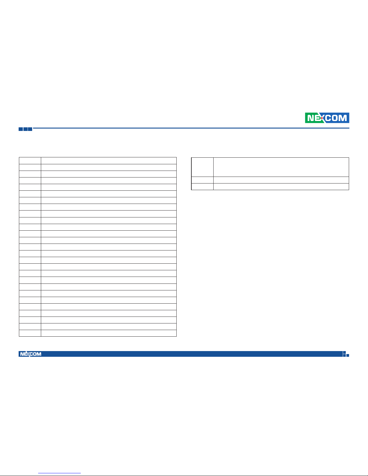
Copyright © 2012 NEXCOM International Co., Ltd. All Rights Reserved.
66
Appendix D: OBDII Module Setup and Command
VTC 7120-BK Series User Manual
Simple Data Protocol: (ASCII CODE)
Data Description
HEAD @
Byte 0 ,
Byte 1 Speed , (0~255) KM/HR
Byte 2 ,
Byte 3 RPM High Byte (RPMHB)
Byte 4 ,
Byte 5 RPM Low Byte(RPMLB) , RPM=RPMHB*256+RPMLB
Byte 6 ,
Byte 7 Engine Loading, (0~100%)
Byte 8 ,
Byte 9 Battery Voltage (BV), = (BV+100)/10 (v)
Byte 10 ,
Byte 11 Engine Temperature( ET), =ET-40°C
Byte 12 ,
Byte 13 Throttle position 0~100 %
Byte 14 ,
Byte 15 Status , Note 2
Byte 16 ,
Byte 17 MAF (0~255), MAF RATE= MAF * 3;
Byte 18 ,
Byte 19 Distance : D1
Byte 20 ,
Byte 21 Distance: D2
Byte 22 ,
Byte 23 FU, Average Fuel Economy (km/L) =Fu /10
Byte 24 ,
Byte 25
Check sum (odd numbers)= Byte1+ Byte3+Byte5+
Byte7+Byte9+Byte11+ Byte13+ Byte15+Byte17+
Byte19+Byte21+Byte23
Byte 26 Carry return ( 0x0D )
Byte 27 Line feed ( 0x0A)
Page 81

Copyright © 2012 NEXCOM International Co., Ltd. All Rights Reserved.
67
Appendix D: OBDII Module Setup and Command
VTC 7120-BK Series User Manual
Simple Data Protocol: (HEX CODE)
Data Description
HEAD @ (=0x40)
Byte 1 Speed , (0~255) KM/HR
Byte 2 RPM High Byte (RPMHB)
Byte 3 RPM Low Byte(RPMLB) , RPM=RPMHB*256+RPMLB
Byte 4 Engine Loading, (0~100%)
Byte 5 Battery Voltage (BV), = (BV+100)/10 (v)
Byte 6 Engine Temperature( ET), =ET-40°C
Byte 7 Engine Loading, (0~100%)
Byte 8 Status , Note 2
Byte 9 MAF (0~255), MAF RATE= MAF * 3;
Byte 10 Distance: D1
Byte 11 Distance: D2
Byte 12 FU, Average Fuel Economy (km/L) =Fu /10
Byte 13
TCheck sum (odd numbers)= Byte1+ Byte2+Byte3+ Byte4+
Byte5+Byte6+ Byte7+ Byte8+Byte9+ Byte10+ Byte11+Byte12
Byte 14 Carry return ( 0x0D )
Byte 15 Line feed ( 0x0A)
NOTE:
1.) Data format : ASCII CODE
@ , 7 8 , 0 E , 7 0 , 0 0 ,0 3 , 9 8 , 2 8 , Status ,MAF,D1,D2,Fu,CS
speed=78 km/hr
rpm=0x0E70= 3696
2.) status:
Bit 7:
0: Normal
1: Emergency Braking ( Acceleration < - 6 m/s2 )
Bit 6:
0: Brake OFF
1: Brake ON
Bit 5:
0: Clutch OFF
1: clutch ON
Bit 4:
0: Cruise Control OFF
1: Cruise Control ON
Bit 3:
0: Brake (ON/OFF) unavailable
1: Brake(ON/OFF) available
Bit 2:
0:Clutch (ON/OFF) unavailable
1: Clutch (ON/OFF) available
Bit 1:
0: Cruise Control (ON/OFF) unavailable
1: Cruise Control (ON/OFF) available
Bit 0:
0: NORMAL
1: DTC ON
2.) Distance = D1*256+D2
3.) Average Fuel Economy =Fu /10
Page 82
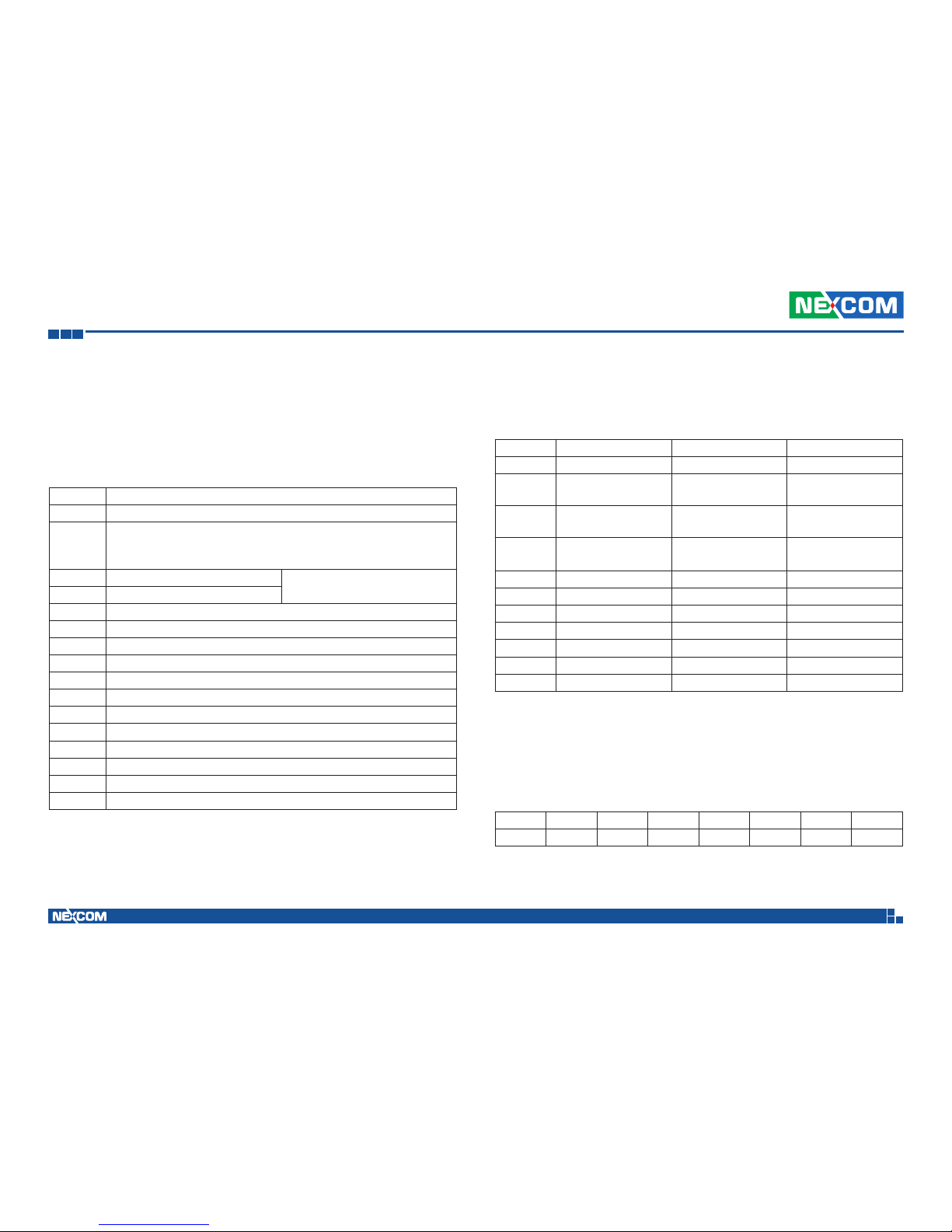
Copyright © 2012 NEXCOM International Co., Ltd. All Rights Reserved.
68
Appendix D: OBDII Module Setup and Command
VTC 7120-BK Series User Manual
J1939 Raw Data Protocol (HEX CODE)
Support for J1939 PGN / SPN access as defined in the J1939 standards.
This function will report all PGNs and their source node on the J1939
network.
Each SPN under this function should be set to a size of 32 bits.
J1939 Format
Byte 0 @ ( =0x40)
Byte 1
Bit4,3,2: Priority
Bit0: Data Page
Bit1,5,6,7:Reversed
Byte 2 PDU Format (PF)
PGN
Byte 3 PDU Specific (PS)
Byte 4 Source Address
Byte 5 Data1
Byte 6 Data2
Byte 7 Data3
Byte 8 Data4
Byte 9 Data5
Byte 10 Data6
Byte 11 Data7
Byte 12 Data8
Byte 13 Check Sum
Byte 14 0x0D
Byte 15 0x0A
J1708 Raw Data Protocol (HEX CODE)
This function will report all MID and PID that broadcasting on the J1708
network. Its data length is not fixed, please refer to SAEJ1708.
J1939 Format PIDs 128-191 PIDs 0-127
Byte 0 @ (= 0x40) @ (= 0x40) @ (= 0x40)
Byte 1
Message
identification (MID)
MID MID
Byte 2
Parameter
identification (PID)
PID PID
Byte 3
Number of data
bytes
Data1 Data1
Byte 4 Data 1 Data2 Check Sum
Byte 5 Data 2 Check Sum 0x0D
Byte 6 …….. 0x0D 0x0A
Byte 7 Data N 0x0A
Byte 8 Check Sum
Byte 9 0x0D
Byte 10 0x0A
PIDs 0-127 describe data parameters that are one byte long.
PIDs 128-191 describe data parameters that consist of two bytes.
PIDs 192-253 The first byte following these PIDs will contain the number of
data parameter bytes.
EX:
MID=128
0x40 0x80 0x15 0x01 0x32 0xC8 0x0D 0x0A
64 128 21 1 50 200 130 10
PID=21 (Engine ECU temperature)
Data=50
Page 83
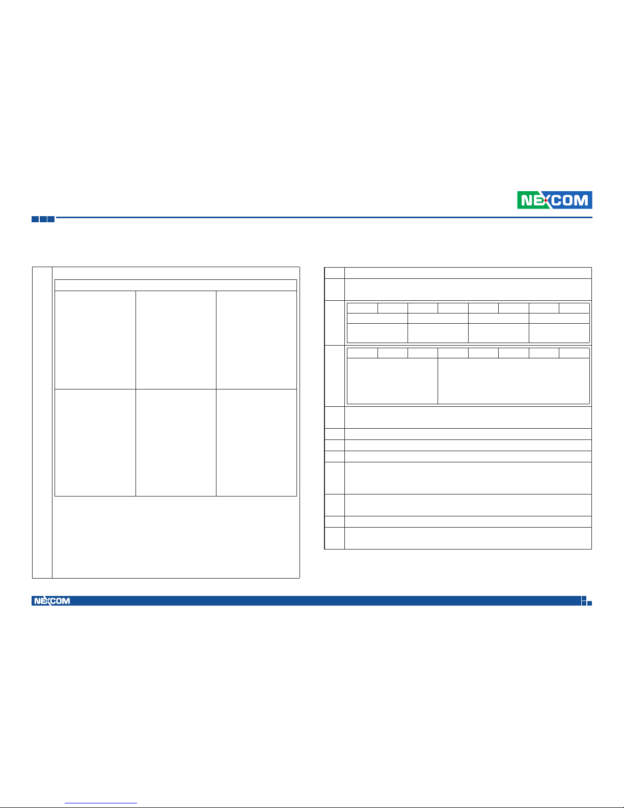
Copyright © 2012 NEXCOM International Co., Ltd. All Rights Reserved.
69
Appendix D: OBDII Module Setup and Command
VTC 7120-BK Series User Manual
J1939 Packaged Messages Protocol
S
ATS: send packaged messages by turns.
Response HEX CODE (default) after ATPH command
Packing 1:
Byte 0:“ @” ,( 0x40)
Byte 1: “1”, (0x31)
Byte 2: #00
Byte 3: #01 ......
Byte 19:#17
Byte 20:
Check sum =
Byte2 + ..+Byte 19
Byte 21: 0X0D
Byte 22: 0X0A
Packing 2:
Byte 0: “ @” ,( 0x40)
Byte 1: “2”,(0x32)
Byte 2: #18
Byte 3: #19 ......
Byte 19:#35
Byte 20:
Check sum = Byte2
+ ..+Byte 19
Byte 21: 0X0D
Byte 22: 0X0A
Packing 3:
Byte 0: “ @” ,( 0x40)
Byte 1: “3”,(0x33)
Byte 2: #36
Byte 3: #37 ......
Byte 19:#53
Byte 20:
Check sum = Byte2
+ ..+Byte 19
Byte 21: 0X0D
Byte 22: 0X0A
Packing 4:
Byte 0:“ @” ,( 0x40)
Byte 1: “a”,(0x41)
Byte 2: #54
Byte 3: #55 ......
Byte 19:#71
Byte 20:
Check sum =
Byte2 + ..+Byte 19
Byte 21: 0X0D
Byte 22: 0X0A
Packing 5:
Byte 0: “ @” ,( 0x40)
Byte 1: “b”,(0x42)
Byte 2: #72
Byte 3: #73 ......
Byte 19:#89
Byte 20:
Check sum = Byte2
+ ..+Byte 19
Byte 21: 0X0D
Byte 22: 0X0A
Packing 6:
Byte 0: “ @” ,( 0x40)
Byte 1: “c”,(0x43)
Byte 2: #90
Byte 3: #91 ......
Byte 14:#102
Byte 19:0
Byte 20:
Check sum = Byte2
+ ..+Byte 19
Byte 21: 0X0D
Byte 22: 0X0A
NOTE :
1. AT#00 ~ AT#102 respond ASCII CODE format data.
2. Packing 6, Byte15~Byte19 not defined (set to ”0”)
3. After ATPA command, byte 21& 22 were ignored.
4. This is the common J1939 measurement overview showing which
measurements are available. Note that not all measurements are
supported by the individual engines.
#00 Speed Low Byte (SLB)
#01
Speed High Byte (SHB)
speed=(SHB*256+SLB)/256
#02
B7 B6 B5 B4 B3 B2 B1 B0
Clutch switch Brake switch NOT USED Cruise control active
00 = pedal released
01 = pedal depressed
00 = pedal released
01 = pedal depressed
00 = switched off
01 = switched on
#03
B7 B6 B5 B4 B3 B2 B1 B0
B7: Emergency brake(-6m/s2)
B6: speed up (6m/s2)
B5: Double Emergency brake
(over -12m/s2)
1: Enable, 0:Disable
PTO state
00000 = off/disabled
00101 = Set
11111 = not available
#04
0.4 % / Bit gain, Accelerator Pedal Position(APP) , 0 to 100 %
APP= Data* 0.4
#05 Engine Total Fuel used 0,5 L / Bit gain , ETF1
#06 Engine Total Fuel used 0,5 L / Bit gain , ETF2
#07 Engine Total Fuel used 0,5 L / Bit gain , ETF3
#08
Engine Total Fuel used 0,5 L / Bit gain , ETF4
Engine Total Fuel used
=((ETF4*256*256*256)+(ETF3*256*256)+(ETF2*256)+ETF1)*0.5
#09
Fuel Level (FL) , 0 to 100 %, 0.4 %/bit
Fuel Level=FL*0.4
#10 RPM Low byte, RL
#11
RPM High byte, RH
RPM= (RH*256+ RL)* 0.125
Page 84
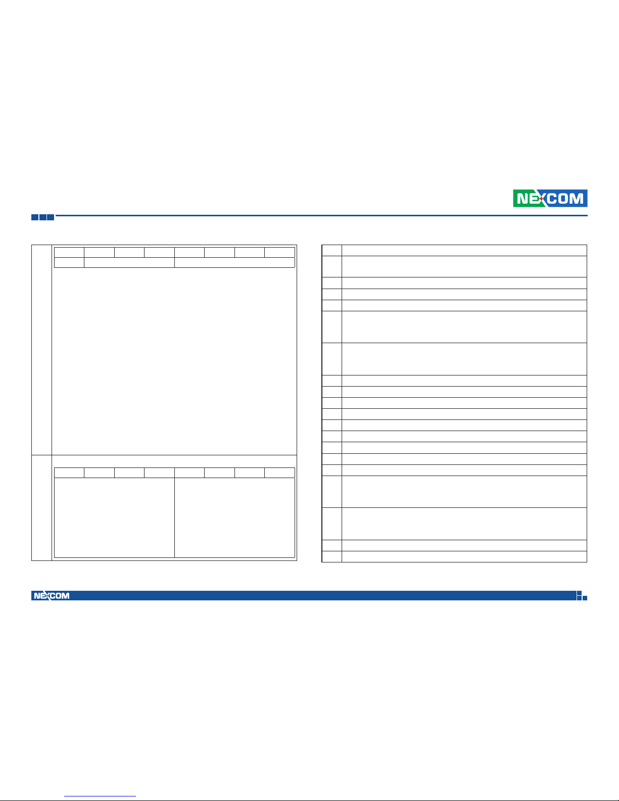
Copyright © 2012 NEXCOM International Co., Ltd. All Rights Reserved.
70
Appendix D: OBDII Module Setup and Command
VTC 7120-BK Series User Manual
#12
B7 B6 B5 B4 B3 B2 B1 B0
NOT USED Engine Starter Mode
B7: 1, Total Vehicle Distance is provided by vehicle ECU
0, Total Vehicle Distance is calculation value
B3~B0:
0000 start not requested
0001 starter active, gear not engaged
0010 starter active, gear engaged
0011 start finished; starter not active after having been actively
engaged ?
(after 50ms mode goes to 0000)?
0100 starter inhibited due to engine already running
0101 starter inhibited due to engine not ready for start (preheating)
0110 starter inhibited due to driveline engaged
0111 starter inhibited due to active immobilizer
1000 starter inhibited due to starter over-temp
1001-1011 Reserved
1100 starter inhibited - reason unknown
1101 error
1111 not available
#13
Axle location The value 0xFF indicates not available.
B7 B6 B5 B4 B3 B2 B1 B0
Axle location Bit-mapped position
number counting front to back facing
forward
F = not available
position number, counting front to
back on the vehicle. B7,B6,B5,B4
Axle location Bit-mapped position
number counting front to back facing
forward.
Tire location Bit-mapped counting left
to right facing forward
F = not available
The low order 4 bits represent a
position number, counting left to right
when facing in the direction of normal
vehicle travel
#14 Axle weight 0.5 kg / Bit gain (Low Byte),AWL
#15
Axle weight 0.5 kg / Bit gain (High Byte), AWH
Weight=(AWH*256+AWL)*0.5
#16 Engine total hours of Operation, EH1
#17 Engine total hours of Operation, EH2
#18 Engine total hours of Operation, EH3
#19
Engine total hours of Operation, EH4
Accumulated
time=((EH4*256*256*256)+(EH3*256*256)+(EH2*256)+EH1)*0.05
#20
|
#27
Vehicle identification number, aabbccddeeffgghh (If the Vehicle ID
contains more than 8 Bytes then #20~#27 are “00”, please use ATI
command to request.
#20 aa
#21 bb
#22 cc
#23 dd
#24 ee
#25 ff
#26 gg
#27 hh
#28 Engine Percent Load At Current Speed ( 0~125 %)
#29
|
#32
SW-version supported for trucks, Version number in the format
ab.cd where this byte represents ASCII code #29 : “a” , #30: ‘b’,
#31:’c’ , #32:’d’
#33
|
#36
High Resolution Total Vehicle Distance, 5 m/bit, 0 to 21,055,406 km
=((D4*256*256*256)+(D3*256*256)+(D2*256)+D1)*0.005 (KM)
#33 D1
#34 D2
Page 85
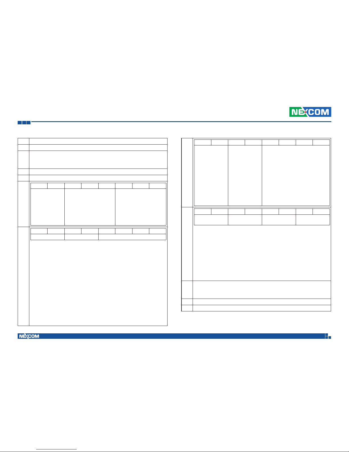
Copyright © 2012 NEXCOM International Co., Ltd. All Rights Reserved.
71
Appendix D: OBDII Module Setup and Command
VTC 7120-BK Series User Manual
#35 D3
#36 D4
#37
|
#38
The distance which can be traveled by the vehicle before the next
service inspection is required
SERV=(V2*256+V1)*5-160635 (KM)
#37 V1
#38 V2
#39
B7 B6 B5 B4 B3 B2 B1 B0
Vehicle
motion(B7,B6):
00 = Vehicle
motion not
detected
01 = vehicle
motion detected
Driv. 2 working stat
state (B5,B4,B3)
°
G
000 = Rest
001 = Driver available
010 = Work
011 = Drive
110 = Error
111 = not available
Driv. 1 working state
(B2,B1,B0):
000 = Rest
001 = Driver available
010 = Work
011 = Drive
110 = Error
111 = not avaiable
#40
B7 B6 B5 B4 B3 B2 B1 B0
Vehicle Overspeed Driver 1 card Driver 1 time related state
Vehicle Over speed (B7,B6)°GIndicates whether the vehicle is
exceeding the legal speed limit set in the tachograph.
00 = No over speed
01 = Over speed Driver 1 card (B5,B4)
00 = Card not present
01 = Card present
Driver 1 time related state (B3,B2,B1,B0)
°
GIndicates if the driver
approaches or exceeds working time limits (or other limits).
0000 = normal
0001 = 15 min bef. 4.5 h
0010 = 4.5 h reached
0011 = 15 min bef. 9 h
0100 = 9 h reached
0101 = 15 min bef. 16 h
0110 = 16h reached
1110 = Error
1111 = not available
#41
B7 B6 B5 B4 B3 B2 B1 B0
NOT USED
Driver 2 card (B5,B4)
00 = Card not
present
01= Card present
Driver 2 time related state (B3,B2,B1,B0)
°
GIndicates if the driver approaches or
exceeds working time limits (or other limits).
0000 = normal
0001 = 15 min bef. 4.5 h
0010 = 4.5 h reached
0011 = 15 min bef. 9 h
0100 = 9 h reached
0101 = 15 min bef. 16 h
0110 = 16h reached
1110 = Error
1111 = not available
#42
B7 B6 B5 B4 B3 B2 B1 B0
Direction indicator
Tachgraph
performance
Handling
information
System event
Direction indicator (B7,B6)°G
00 = Forward
01 = Reverse Tachgraph performance (B5,B4)
00 = Normal performance
01 = Performance analysis Handling information (B3,B2)
00 = no handling information
01 = handling information System event (B1,B0)
00 = no tachogr. Event
01 = tachogr. Event
#43
|
#44
Tachogr. vehicle speed 1/256 km/h Bit gain
Speed= ((VS2*256)+VS1)/256
#43 VS1
#44 VS2
Page 86
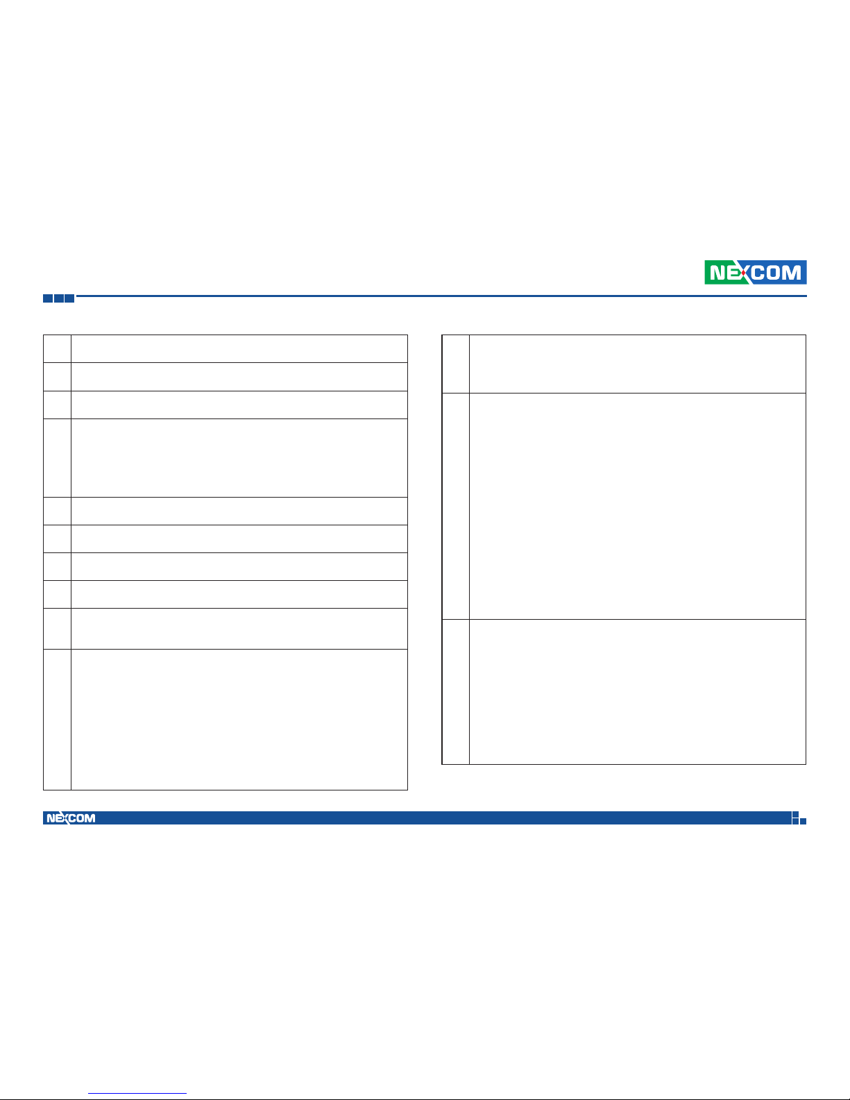
Copyright © 2012 NEXCOM International Co., Ltd. All Rights Reserved.
72
Appendix D: OBDII Module Setup and Command
VTC 7120-BK Series User Manual
#45
Engine Coolant Temperature(ECT) , -40 to 210 deg C
ECT=data-40°C
#46
Engine Turbocharger Boost Pressure(ETBP), 2 kPa/bit , 0~500 KPA
ETPB=data *2 (KPA)
#47
Engine Intake Manifold 1 Temperature(EIMT) , -40 to 210 deg C
EIMT=data-40°C
#48
Bit7,6 Anti-Lock Braking (ABS) Active
°
G
00 - ABS passive but installed
01 - ABS active
10 – Reserved
11 - Not available
Bit5~Bit0: Resvered.
#49
Brake Pedal Position (BPP), 0.4 %/bit, 0~100%
BPP=data*0.4 (%)
#50
Parking and/or Trailer Air Pressure(PTAP), 8 kPa/bit
PTAP=data *8 (KPA)
#51
Service Brake Air Pressure Circuit #1 (SBAPC1), 8 kPa/bit
SBAPC1=data*8 (KPA)
#52
Service Brake Air Pressure Circuit #2 (SBAPC2), 8 kPa/bit
SBAPC2=data*8 (KPA)
#53
Parking Brake Switch
00 = Parking brake not set
01 = Parking brake set
#54
Bit 1 ,Bit 0: Diagnostics supported
00 = diagnostics is not supported
01 = diagnostics is supported
10 = reserved
11 = don´t care
Bit 3 ,Bit 2: Requests supported
00 = request is not supported
01= request is supported
10 = reserved
11 = don´t care
Bit4~Bit7:Resvered
#55
|
#56
Ambient Air Temperature: Temperature of air surrounding vehicle.
AAT=(AATH* 256+AATL)*0.03125 -273 deg C
#55: AATL
#56: AATH
#57
Door Control 1:
Bit 7,Bit6: Status 2 of doors
00 = all bus doors disabled
01 = at least 1 bus door enabled
10 = error
11 = not available
Bit 5, Bit4: Ramp/Wheel chairlift
00 = inside bus
01 = outside bus
10 = Error
11 = not available
Bit 3,2,1,0 : Position of doors
0000 = at least 1 door is open
0001 = closing last door
0010 = all doors closed
1110 = Error
1111 = not available
#58
|
#56
Door Control 2, #58~#65
Lock Status:
locked→doors cannot be operated by the driver or a passenger
unlocked→door may be operated by the driver or a passenger
Open Status:
closed→door is completely closed
open→door is not completely closed
Enable Status:
disabled→door cannot be opened by a passenger
enabled→door can be opened by a passenger
Page 87
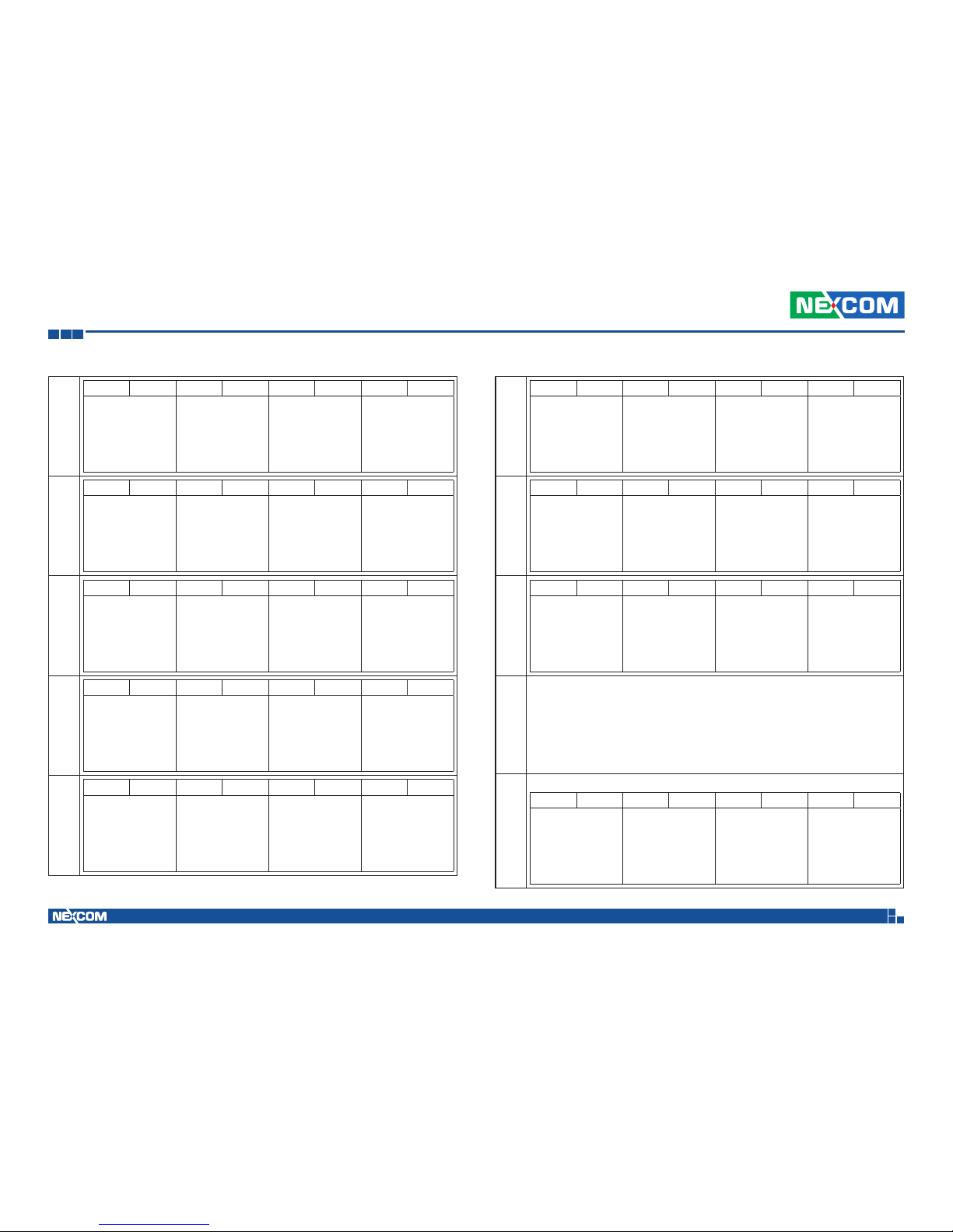
Copyright © 2012 NEXCOM International Co., Ltd. All Rights Reserved.
73
Appendix D: OBDII Module Setup and Command
VTC 7120-BK Series User Manual
#58
B7 B6 B5 B4 B3 B2 B1 B0
Bit 7, Bit 6: Lock
Status Door 2
00 = Unlocked
01 = Locked
10 = Error
11 = Not available
Bit 5,Bit 4: Enable
Status Door 1
00 = Disabled
01 = Enabled
10 = Error
11 = Not available
Bit 3,Bit 2: Open
Status Door 1
00 = Closed
01 = Open
10 = Error
11 = Not available
Bit 1,Bit 0: Lock
Status Door 1
00 = Unlocked
01 = Locked
10 = Error
11 = Not available
#59
B7 B6 B5 B4 B3 B2 B1 B0
Bit 7, Bit 6: Open
Status Door 3
00 = Closed
01 = Open
10 = Error
11 = Not available
Bit 5, Bit 4: Lock
Status Door 3
00 = Unlocked
01 = Locked
10 = Error
11 = Not available
Bit 3, Bit 2: Enable
Status Door 2
00 = Disabled
01 = Enabled
10 = Error
11 = Not available
Bit 1, Bit 0: Open
Status Door 2
00 = Closed
01 = Open
10 = Error
11 = Not available
#60
B7 B6 B5 B4 B3 B2 B1 B0
Bit 7, Bit 6: Enable
Status Door 4
00 = Disabled
01 = Enabled
10 = Error
11 = Not available
Bit 5, Bit 4: Open
Status Door 4
00 = Closed
01 = Open
10 = Error
11 = Not available
Bit 3, Bit 2: Lock
Status Door 4
00 = Unlocked
01 = Locked
10 = Error
11 = Not available
Bit 1, Bit 0: Enable
Status Door 3
00 = Disabled
01 = Enabled
10 = Error
11 = Not available
#61
B7 B6 B5 B4 B3 B2 B1 B0
Bit 7, Bit 6: Lock
Status Door 6
00 = Unlocked
01 = Locked
10 = Error
11 = Not available
Bit 5, Bit 4: Enable
Status Door 5
00 = Disabled
01 = Enabled
10 = Error
11 = Not available
Bit 3, Bit 2: Open
Status Door 5
00 = Closed
01 = Open
10 = Error
11 = Not available
Bit 1, Bit 0: Lock
Status Door 5
00 = Unlocked
01 = Locked
10 = Error
11 = Not available
#62
B7 B6 B5 B4 B3 B2 B1 B0
Bit 7, Bit 6: Open
Status Door 7
00 = Closed
01 = Open
10 = Error
11 = Not available
Bit 5, Bit 4: Lock
Status Door 7
00 = Unlocked
01 = Locked
10 = Error
11 = Not available
Bit 3, Bit 2: Enable
Status Door 6
00 = Disabled
01 = Enabled
10 = Error
11 = Not available
Bit1, Bit 0: Open
Status Door 6
00 = Closed
01 = Open
10 = Error
11 = Not available
#63
B7 B6 B5 B4 B3 B2 B1 B0
Bit 7, Bit 6: Enable
Status Door 8
00 = Disabled
01 = Enabled
10 = Error
11 = Not available
Bit 5, Bit 4: Open
Status Door 8
00 = Closed
01 = Open
10 = Error
11 = Not available
Bit 3, Bit 2: Lock
Status Door 8
00 = Unlocked
01 = Locked
10 = Error
11 = Not available
Bit1, Bit 0: Enable
Status Door 7
00 = Disabled
01 = Enabled
10 = Error
11 = Not available
#64
B7 B6 B5 B4 B3 B2 B1 B0
Bit 7, Bit 6: Lock
Status Door 10
00 = Unlocked
01 = Locked
10 = Error
11 = Not available
Bit 5, Bit 4: Enable
Status Door 9
00 = Disabled
01 = Enabled
10 = Error
11 = Not available
Bit 3, Bit 2: Open
Status Door 9
00 = Closed
01 = Open
10 = Error
11 = Not available
Bit1, Bit 0: Lock
Status Door 9
00 = Unlocked
01 = Locked
10 = Error
11 = Not available
#65
B7 B6 B5 B4 B3 B2 B1 B0
Bit 3, Bit 2: Enable
Status Door 10
00 = Disabled
01 = Enabled
10 = Error
11 = Not available
Bit1, Bit 0: Open
Status Door 10
00 = Closed
01 = Open
10 = Error
11 = Not available
#66
|
#71
Time / Date:
#66 : Second=data * 0.25
#67 : Minutes=data
#68 : Hours=data
#69 : Month=data
#70 : Day=data * 0.25
#71 : Year=data-1985 (1985 to 2235 years)
#72
Alternator Status
B7 B6 B5 B4 B3 B2 B1 B0
Bit 7, Bit6:
Alternator Status 4
00 = not charging
01 = charging
10 = error
11 = not available
Bit 5, Bit4:
Alternator Status 3
00 = not charging
01 = charging
10 = error
11 = not available
Bit 3, Bit 2:
Alternator Status 2
00 = not charging
01 = charging
10 = error
11 = not available
Bit 1, Bit 0:
Alternator Status 1
00 = not charging
01 = charging
10 = error
11 = not available
Page 88
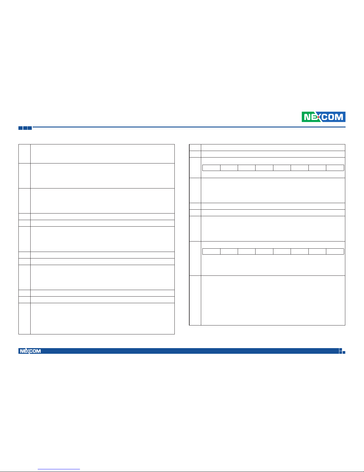
Copyright © 2012 NEXCOM International Co., Ltd. All Rights Reserved.
74
Appendix D: OBDII Module Setup and Command
VTC 7120-BK Series User Manual
#73
Selected Gear = data -125negative gear are reverse gears
00000000 = neutral
11111011 = park
#74
Current Gear=data-125
negative gear are reverse gears
00000000 = neutral
11111011 = park
#75
|
#76
Bellow Pressure Front Axle Left
Information of the pressure of the air suspension bellow at the left
side of the front axle
Pressure= ((BPFAL2*256)+BPFAL1)* 0.1 ,KPA
#75 BPFAL1
#76 BPFAL2
#77
|
#78
Bellow Pressure Front Axle Right
Information of the pressure of the air suspension bellow at the left
side of the front axle
Pressure= ((BPFAR2*256)+BPFAR1)* 0.1 ,KPA
#77 BPFAR1
#78 BPFAR2
#79
|
#80
Bellow Pressure Rear Axle Left
Information of the pressure of the air suspension bellow at the left
side of the front axle
Pressure= ((BPRAL2*256)+BPRAL1)* 0.1 ,KPA
#79 BPRAL1
#80 BPFAR2
#81
|
#82
Bellow Pressure Rear Axle Right
Information of the pressure of the air suspension bellow at the left
side of the
front axle
Pressure= ((BPRAR2*256)+BPRAR1)* 0.1 ,KPA
#81 BPRAL1
#82 BPFAR2
#83
|
#90
Driver’s Identification (Driver 1 & Driver 2 identification)
#83 #84 #85 #86 #87 #88 #89 #90
The driver ID is only available if a digital tachograph is present
#91
|
#92
Engine Fuel Rate (EFR). Amount of fuel consumed by engine per
liter of hour.
EFR=(EFR2*256+EFR1)* 0.05 , L/h
Data Range: 0 to 3,212.75 L/h
#91 EFR1
#92 EFR2
#93
|
#94
Engine Instantaneous Fuel Economy(EIFE). Current fuel economy at
current vehicle velocity.
EIFE=(EIFE2*256+EIFE1) / 512 , km/L
Data Range: 0 to 125.5 km/L
#95
|
#
102
FMS Tell Tale Status
#95 #96 #97 #98 #99 #100 #101 #102
The Tell Tale Status information is derived from information
displayed to the
driver’s dashboard.
#95
Bit 3,2,1,0: Telltale Block ID
Bit 7,6,5,4: Telltale Status 1
1000 = off
1001 = Cond. Red
1010 = Cond. Yellow
1011 = Cond. Info
1100–1110 = Reserved
1111 = not available
Page 89

Copyright © 2012 NEXCOM International Co., Ltd. All Rights Reserved.
75
Appendix D: OBDII Module Setup and Command
VTC 7120-BK Series User Manual
#96
Bit 3,2,1,0: Telltale Status 2
1000 = off
1001 = Cond. Red
1010 = Cond. Yellow
1011 = Cond. Info
1100–1110 = Reserved
1111 = not available
Bit 7,6,5,4: Telltale Status 3
1000 = off
1001 = Cond. Red
1010 = Cond. Yellow
1011 = Cond. Info
1100–1110 = Reserved
1111 = not available
#97
Bit 3,2,1,0: Telltale Status 4
1000 = off
1001 = Cond. Red
1010 = Cond. Yellow
1011 = Cond. Info
1100–1110 = Reserved
1111 = not available
Bit 7,6,5,4: Telltale Status 5
1000 = off
1001 = Cond. Red
1010 = Cond. Yellow
1011 = Cond. Info
1100–1110 = Reserved
1111 = not available
#98
Bit 3,2,1,0: Telltale Status 6
1000 = off
1001 = Cond. Red
1010 = Cond. Yellow
1011 = Cond. Info
1100–1110 = Reserved
1111 = not available
Bit 7,6,5,4: Telltale Status 7
1000 = off
1001 = Cond. Red
1010 = Cond. Yellow
1011 = Cond. Info
1100–1110 = Reserved
1111 = not available
#99
Bit 3,2,1,0: Telltale Status 8
1000 = off
1001 = Cond. Red
1010 = Cond. Yellow
1011 = Cond. Info
1100–1110 = Reserved
1111 = not available
Bit 7,6,5,4: Telltale Status 9
1000 = off
1001 = Cond. Red
1010 = Cond. Yellow
1011 = Cond. Info
1100–1110 = Reserved
1111 = not available
Page 90

Copyright © 2012 NEXCOM International Co., Ltd. All Rights Reserved.
76
Appendix D: OBDII Module Setup and Command
VTC 7120-BK Series User Manual
#
100
Bit 3,2,1,0: Telltale Status 10
1000 = off
1001 = Cond. Red
1010 = Cond. Yellow
1011 = Cond. Info
1100–1110 = Reserved
1111 = not available
Bit 7,6,5,4: Telltale Status 11
1000 = off
1001 = Cond. Red
1010 = Cond. Yellow
1011 = Cond. Info
1100–1110 = Reserved
1111 = not available
#
101
Bit 3,2,1,0: Telltale Status 12
1000 = off
1001 = Cond. Red
1010 = Cond. Yellow
1011 = Cond. Info
1100–1110 = Reserved
1111 = not available
Bit 7,6,5,4: Telltale Status 13
1000 = off
1001 = Cond. Red
1010 = Cond. Yellow
1011 = Cond. Info
1100–1110 = Reserved
1111 = not available
#
102
Bit 3,2,1,0: Telltale Status 14
1000 = off
1001 = Cond. Red
1010 = Cond. Yellow
1011 = Cond. Info
1100–1110 = Reserved
1111 = not available
Bit 7,6,5,4: Telltale Status 15
1000 = off
1001 = Cond. Red
1010 = Cond. Yellow
1011 = Cond. Info
1100–1110 = Reserved
1111 = not available
Page 91

Copyright © 2012 NEXCOM International Co., Ltd. All Rights Reserved.
77
Appendix D: OBDII Module Setup and Command
VTC 7120-BK Series User Manual
J1708 Packaged Messages Protocol
S
Once AT1708 SLEEP, it can wake it up.
Start to send data by 3 packing, response HEX CODE
Packing 1:
Byte 0: “ @” , 0x40;
Byte 1: 4
Byte 2: #00
Byte 3: #01
Byte 4: #02
Byte 5: #03
Byte 6: #04
Byte 7: #05
Byte 8: #06
Byte 9: #07
Byte 10: #08
Byte 11: #09
Byte 12: #10
Byte 13: #11
Byte 14: #12
Byte 15: #13
Byte 16: #14
Byte 17: #15
Byte 18: #16
Byte 19: #17
Byte 20: Check sum
= Byte2 + ..+Byte 19
Byte 21: 0X0D
Byte 22: 0X0A
Packing 2:
Byte 0: “ @” , 0x40;
Byte 1: 5
Byte 2: #18
Byte 3: #19
Byte 4: #20
Byte 5: #21
Byte 6: #22
Byte 7: #23
Byte 8: #24
Byte 9: #25
Byte 10: #26
Byte 11: #27
Byte 12: #28
Byte 13: #29
Byte 14: #30
Byte 15: #31
Byte 16: #32
Byte 17: #33
Byte 18: #34
Byte 19: #35
Byte 20: Check sum
= Byte2 + ..+Byte 19
Byte 21: 0X0D
Byte 22: 0X0A
Packing 3:
Byte 0: “ @” , 0x40;
Byte 1: 6
Byte 2: #36
Byte 3: #37
Byte 4: #38
Byte 5: #39
Byte 6: #40
Byte 7: #41
Byte 8: #42
Byte 9: #43
Byte 10: #44
Byte 11: #45
Byte 12: #46
Byte 13: #47
Byte 14: #48
Byte 15: #49
Byte 16: #50
Byte 17: #51
Byte 18: #52
Byte 19: #53
Byte 20:Check sum
= Byte2 + ..+Byte 19
Byte 21: 0X0D
Byte 22: 0X0A
Packing 4 & 5 will display only there is trouble code occurrence.
Packing 4:
Byte 0: “ @”
Byte 1: 7
Byte 2:a
Byte 3:b
Byte 4:c
Byte 5:a
Byte 6:b
Byte 7:c
Byte 8:a
Byte 9:b
Byte 10:c
Byte 11:a
Byte 12:b
Byte 13:c
Byte 14:a
Byte 15:b
Byte 16:c
Byte 17: Check sum
= Byte2 + ..+Byte 21
Byte 18: 0X0D
Byte 19: 0X0A
Packing 5:
Byte 0: “ @”
Byte 1: 8
Byte 2:a
Byte 3:b
Byte 4:c
Byte 5:a
Byte 6:b
Byte 7:c
Byte 8:a
Byte 9:b
Byte 10:c
Byte 11:a
Byte 12:b
Byte 13:c
Byte 14:a
Byte 15:b
Byte 16:c
Byte 17: Check sum
= Byte2 + ..+Byte 21
Byte 18: 0X0D
Byte 19: 0X0A
a — MID
b — SID or PID of a standard diagnostic code.
C — Diagnostic code character.
Bits 4-1: Failure mode identifier (FMI)
NOTE : The #00~#52 command respond that data are ASCII code.
Page 92
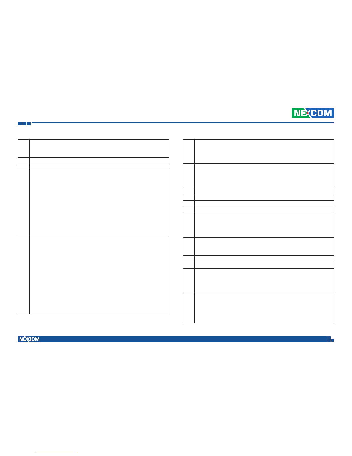
Copyright © 2012 NEXCOM International Co., Ltd. All Rights Reserved.
78
Appendix D: OBDII Module Setup and Command
VTC 7120-BK Series User Manual
#00
|
#01
Road Speed—Indicated vehicle velocity
Maximum Range: 0.0 to 205.2 km/h (0.0 to 127.5 mph)
speed=(SHB*256+SLB)/256
#00 Speed Low Byte (SLB)
#01 Speed High Byte (SHB)
#02
Cruise Control Status—State of the vehicle velocity control system
(active, not active), and system switch (on, off), for various system
operating modes.
Bit 8: cruise mode 1=active/0=not active
Bit 7: clutch switch 1=on/0=off
Bit 6: brake switch 1=on/0=off
Bit 5: accel switch 1=on/0=off
Bit 4: resume switch 1=on/0=off
Bit 3: coast switch 1=on/0=off
Bit 2: set switch 1=on/0=off
Bit 1: cruise control switch 1=on/0=off
#03
Brake Stroke Status—Identifies the current state of the vehicle
foundation brakes.
Bit 8-5: Axle number 1 to 16 (represented as 0 to 15)
Bit 4-2: Brake status/Stroke adjustment
000 = OK
001 = Out of adjustment
010 = Delay brake return
011 = Brake pads worn
100 = Delayed brake application
101 = Reserved
110 = Error
111 = Not available
Bit 1: 1 = Left wheel, 0 = Right wheel
#04
Percent Accelerator Pedal Position(PAPP)—Ratio of actual
accelerator pedal position to maximum pedal position.
Maximum Range: 0.0 to 102.0%
PAPP= Data* 0.4
#05
|
#08
Total Fuel Used (Natural Gas)—Accumulated amount of fuel used
during vehicle operation.
Maximum Range: 0.0 to 2 147 483 648 kg (0.0 to 4 724 464 025 lb)
TFU=((ETF4*256*256*256)+(ETF3*256*256)+(ETF2*256)+ETF1)*0.473
#05 Engine Total Fuel used 0473 L / Bit gain , ETF1
#06 Engine Total Fuel used 0,473 L / Bit gain , ETF2
#07 Engine Total Fuel used 0,473 L / Bit gain , ETF3
#08 Engine Total Fuel used 0,473 L / Bit gain , ETF4
#09
Fuel Level—Ratio of volume of fuel to the total volume of the
primary fuel storage container.
Maximum Range: 0.0 to 127.5%
Fuel Level=FL * 0.5 %
#10
|
#11
Engine Speed (RPM)—Rotational velocity of crankshaft.
Maximum Range: 0.0 to 16383.75 rpm
RPM= (RH*256+ RL)* 0.25
#10 RPM Low byte, RL
#11 RPM High byte, RH
#12
Engine Oil Pressure(EOP)—Gage pressure of oil in engine
lubrication system as provided by oil pump.
Maximum Range: 0.0 to 879.0 kPa (0.0 to 127.5 lbf/in2)
EOP=data * 3.45 KPA
#13
Throttle Position(TP)—The position of the valve used to regulate the
supply of a fluid, usually air or fuel/air mixture, to an engine. 0%
represents no supply and 100% is full supply.
Maximum Range: 0.0 to 102.0%
TP= data * 0.4%
Page 93
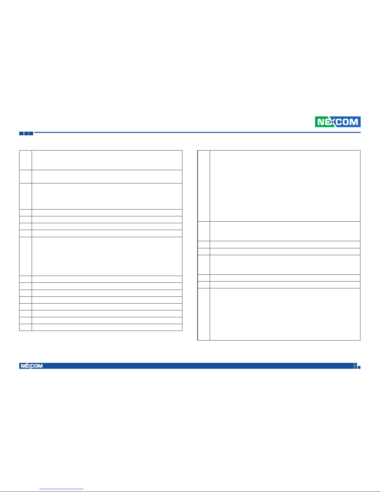
Copyright © 2012 NEXCOM International Co., Ltd. All Rights Reserved.
79
Appendix D: OBDII Module Setup and Command
VTC 7120-BK Series User Manual
#14
Cargo Weight—The force of gravity of freight carried.
Maximum Range: 0.0 to 1 166 056.9 N (0.0 to 262 140.0 lbf)
(Low Byte),AWL
#15
(High Byte), AWH
Weight=(AWH*256+AWL)* 17.792 N
#16
Total Engine Hours(TEH)—Accumulated time of operation of
engine.
Maximum Range: 0.0 to 214 748 364.8 h
TEH=((EH4*256*256*256)+(EH3*256*256)+(EH2*256)+EH1)*0.05
#16 Engine total hours of Operation, EH1
#17 Engine total hours of Operation, EH2
#18 Engine total hours of Operation, EH3
#19 Engine total hours of Operation, EH4
#20
|
#27
#85
|
#96
Vehicle Identification Number—Vehicle Identification Number (VIN)
as assigned by the vehicle manufacturer.
Vehicle identification number, aabbccddeeffgghh
“ATI” command can show max 20 character VIN
#20 aa
#21 bb
#22 cc
#23 dd
#24 ee
#25 ff
#26 gg
#27 hh
#28
PTO Engagement Control Status
PTO output status:
Bits 8-5: Reserved—all bits set to 1
Bits 4-3: PTO #2 engagement actuator status
Bits 2-1: PTO #1 engagement actuator status
NOTE—Each status will be described using the following
nomenclature:
00 Off/Not active
01 On/Active
10 Error condition
11 Not available
#29
|
#30
Average Fuel Economy
AFE=((AFE2*256)+AFE1) *1.660 72 x 10-3 km/L
#29 AFE1
#30 AFE2
#31
|
#32
Mass Air Flow—Mass air flow measured at the fresh air intake
MAF=((MAF2*256)+MF1)* 0.125 kg/min
#31 MAF1
#32 MAF2
#33
|
#36
Total Vehicle Distance(TVD)—Accumulated distance travelled by
vehicle during its operation.
Maximum Range: 0.0 to 691489743 km (0.0 to 429 496 729.5 mi)
Bit Resolution: 0.161 km (0.1 mi)
TVD=((D4*256*256*256)+(D3*256*256)+(D2*256)+D1)*0.161 (KM)
If vehicle dose not provide TVD, AT1708 replace the information
with the calculated distance, deviation is 0.5%, The first time
connection AT1708 please command ATR to clear distance memory.
Page 94
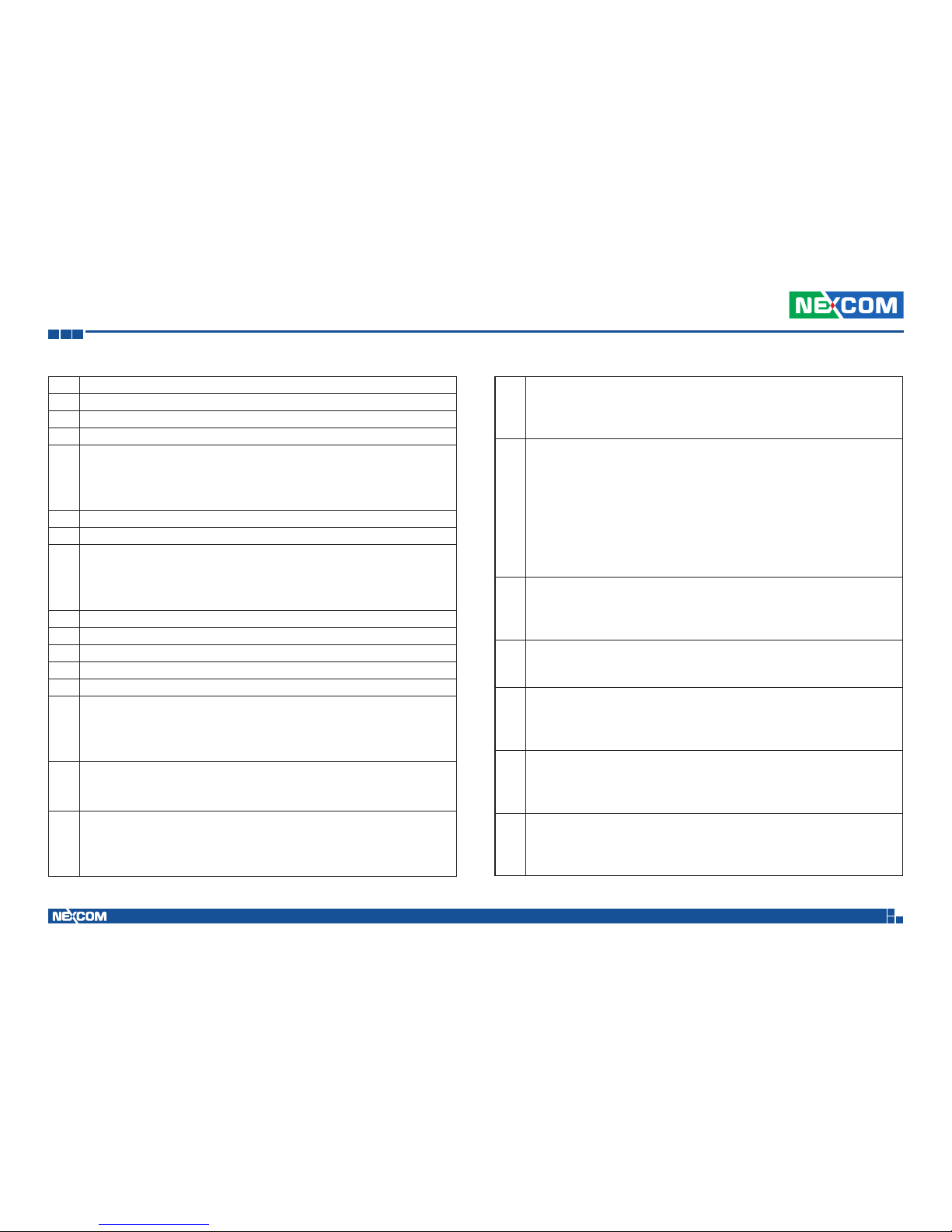
Copyright © 2012 NEXCOM International Co., Ltd. All Rights Reserved.
80
Appendix D: OBDII Module Setup and Command
VTC 7120-BK Series User Manual
#33 D1
#34 D2
#35 D3
#36 D4
#37
|
#38
Fuel Rate (Instantaneous)—Amount of fuel consumed by engine per
unit of time.
Maximum Range: 0.0 to 1.076 65 L/s
FR=(V2*256+V1) * 16.428 x 106 L/s
#37 V1
#38 V2
#39
|
#40
Total Vehicle Hours(TVH)—Accumulated time of operation of
vehicle.
Maximum Range: 0.0 to 214 748 364.8 h
TVH=((H4*256*256*256)+(H3*256*256)+(H2*256)+H1)*0.05 (H)
#39 H1
#40 H2
#41 H3
#42 H4
#43 Reserved
#44
Percent Engine Load(PEL)—Ratio of current output torque to
maximum torque available at the current engine speed.
Maximum Range: 0.0 to 127.5%
PEL=data * 0.5%
#45
Engine Coolant Temperature(ECT) ,
Maximum Range: 0.0 to 255.0 °F
ECT= data °F
#46
Boost Pressure (BP)—Gage pressure of air measured downstream
on the compressor discharge side of the turbocharger.
Maximum Range: 0.0 to 219.8 kPa (0.0 to 31.875 lbf/in2)
PB=data * 0.862 (KPA)
#47
Intake Manifold Temperature (IMT)—Temperature of precombustion
air found in intake manifold of engine air supply system.
Maximum Range: 0.0 to 255.0 °F
IMT=data °F
#48
ABS Control Status
Bits 8-7: ABS off-road function switch
Bits 6-5: ABS retarder control
Bits 4-3: ABS brake control
Bits 2-1: ABS warning lamp
00 Off/Not active
01 On/Active
10 Error condition
11 Not available
#49
Parking Brake Switch Status—Identifies the state (active/inactive) of
the parking brake switch.
Bit 8: 1=active/0=inactive
Bits 7-1: Undefined
#50
Brake Application Pressure (BAP)
Maximum Range: 0.0 to 1055 kPa (0.0 to 153.0 lbf/in2)
BAP=data *4.14 kPa
#51
Brake Primary Pressure (BPP)—Gage pressure of air in the primary,
or supply side, of the air brake system.
Maximum Range: 0.0 to 1055 kPa (0.0 to 153.0 lbf/in2)
BPP=data* 4.14 (KPA)
#52
Brake Secondary Pressure—Gage pressure of air in the secondary,
or service side, of the air brake system.
Maximum Range: 0.0 to 1055 kPa (0.0 to 153.0 lbf/in2)
BPP=data* 4.14 (KPA)
#53
Road Speed Limit Status :State (active or not active) of the system
used to limit maximum vehicle velocity.
Bit 8: 1=active/0=not active
Bits 7-1: Undefined
Page 95
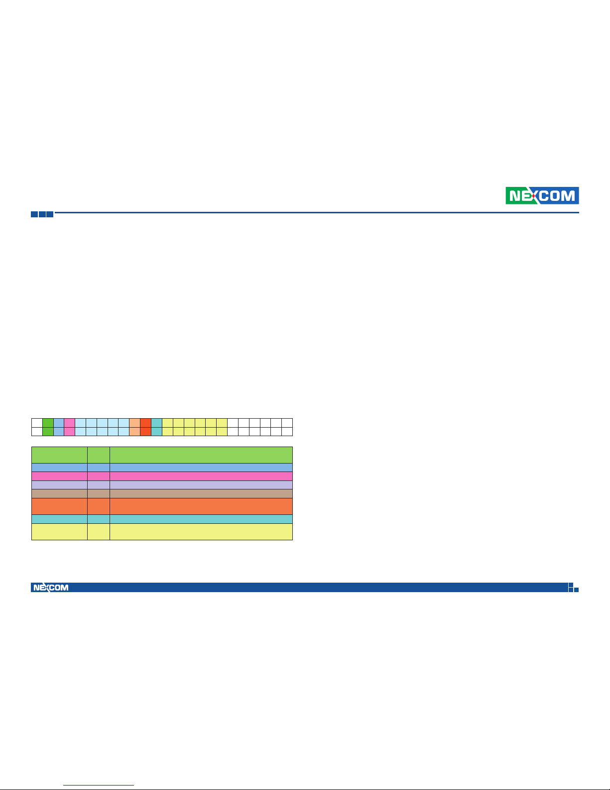
Copyright © 2012 NEXCOM International Co., Ltd. All Rights Reserved.
81
Appendix D: OBDII Module Setup and Command
VTC 7120-BK Series User Manual
J1708 Command Example
1.) >AT#h,
Response: “Data1” “Data2” “H0D” “H3E” by ASCII CODE.
EX1:
AT#1, to get vehicle speed, if speed is 255,
Display,
FF
>
(H46,H46, H0D,H3E).
2.) Trouble code :
40 37 80 8 CA 80 A AA 80 B AA 80 C AA 80 1 AA FC D A
Trouble code :
MID 128( H80)
PID 8(H8)
Diagnostic code character ( CA), FMI= A , bit4~bit1
4.) ATI : request vehicle ID,
2A 31 47 31 4A 46 32 37 57 37 47 4A 31 37 38 32 32 37 0 0 0 27 0D 0A
1 G 1 G F 2 7 W 8 G J 1 7 8 2 2 7 CS
Country Manufactured 1
U.S.A.(1 or 4), Canada (2), Mexico (3), Japan (J), Korea (K), England (S),
Germany (W), Italy (Z)
Manufacturer G
Vehicle Type 1
Vehicle Features JF27W
Accuracy Check Digit 8
Model Year G
1988 (J), 1989 (K), 1990 (L), 1991 (M), 1992 (N), 1993 (P), 1994 (R), 1995 (S),
1996 (T), 199 7(V), 1998 (W), 1999 (X), 2000 (Y), 2001(1), 2002 (2), 2003 (3)…..
Production Plant J
Sequential Number 178227
The sequence of the vehicle for production as it rolled of the manufacturers
assembly line.
Page 96
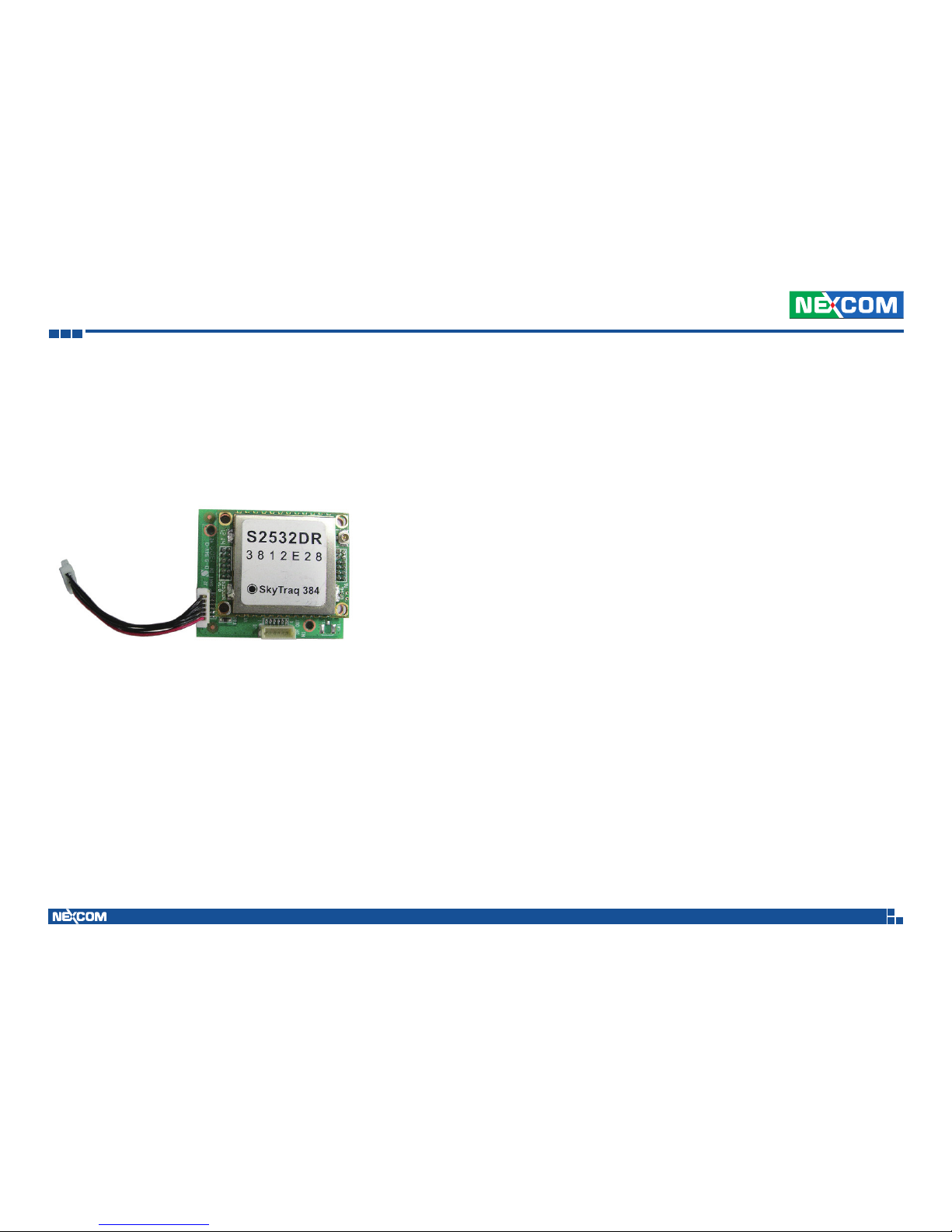
Copyright © 2012 NEXCOM International Co., Ltd. All Rights Reserved.
82
VTC 7120-BK Series User Manual
Appendix E: Pin Definition for GPS with Dead Reckoning
Appendix E: Pin Definition for GPS Dead Reckoning Module -VIOB-GPS-DR01
S2532DR Overview Technical Specifications
Receiver Type L1 C/A code, 65-channel Venus 6 engine
Accuracy Position 2.5m CEP
Velocity 0.1m/sec
Time 300ns
Startup Time 1 second hot start under open sky
< 29 second warm start under open sky (average)
29 second cold start under open sky (average)
Reacquisition 1s
Sensitivity -148dBm cold start
-161dBm tracking
Update Rate 1Hz
Operational Limits Altitude < 18,000m or velocity < 515m/s
Serial Interface 3.3V LVTTL level
Protocol NMEA-0183 V3.01
PGGA, GPGLL, GPGSA, GPGSV, GPRMC, GPVTG*1
38400 baud, 8, N, 1
Datum Default WGS-84
User definable
Input Voltage 3.3V DC +/-10%
Input Current ~40mA tracking
Dimension 25mm L x 32mm W
Weight 5g
Interface Connector two 12-pin male header, 1.27mm pitch
Operating Temperature -40oC ~ +85oC
Storage Temperature -55 ~ +100oC
Humidity 5% ~ 95%
The S2532DR GPS Dead-Reckoning receiver module combines GPS
position data, gyroscope data (measuring turning angle), and odometer
data (measuring distance traveled) to formulate position solution. This
enables accurate navigation solution in poor signal environment or signal
blocked area such as inside tunnels. The S2532DR is ideal for applications
requiring accurate continuous navigation with 100% availability.
The S2532DR features 65 channel GPS receiver with fast time to first fix and
improved -148dBm cold start sensitivity. The superior cold start sensitivity allows
it to acquire, track, and get position fix autonomously in difficult weak signal
environment. The receiver’s -161dBm tracking sensitivity allows continuous
position coverage in nearly all application environments. The high performance
search engine is capable of testing 8,000,000 time-frequency hypotheses
per second, offering industry-leading signal acquisition and TTFF speed.
Page 97
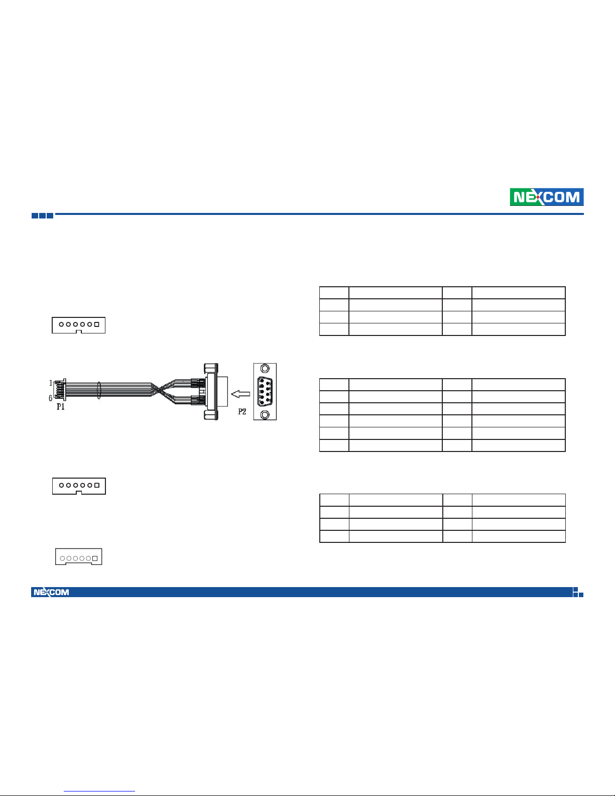
Copyright © 2012 NEXCOM International Co., Ltd. All Rights Reserved.
83
VTC 7120-BK Series User Manual
Appendix E: Pin Definition for GPS with Dead Reckoning
VIOB-GPS-DR01 consists of S2532DR and cables.
Here are the connector and cable pin definition for VIOB-GPS-DR01.
(1) Connect VIOB-GPS-DR01 and DB9 Cable
(On VIOB-GPS-DR01)
(2) Connect VIOB-GPS-DR01 and VTC 71 Carrier Board with Cable
(On VIOB-GPS-DR01)
C. VIOB-GPS-DR01 to DB9 Cable (6P TO D-SUB-9M)
Pin Definition Pin Definition
1 GND 4 GPIO22
2 DIRECTION 5 1PPS
3 ODOMETER 6 GND
Pin Definition Pin Definition
1 +V3.3S 4 SP_TX1
2 GND 5 GPS_LED#
3 SP_RX1 6 GPS_BAT
Pin Definition Pin Definition
1 1PPS 6 GND
2 GPIO22 7 NC
3 NC 8 NC
4 ODOMETER 9 GND
5 DIRECTION
Connector pin definition of P2
Connector pin definition of P1
Connector pin definition of J9
1
1
1
6
6
6
(On VTC 71 Carrier Board)
A. Connector type: 1x6 6-pin header
B. Connector location: J9
A. Connector type: 1x6 6-pin header
B. Connector location: J2
A. Connector type: 1x6 6-pin header
B. Connector location: J1
NOTE: Onboard uBlox NEO-6Q GPS module can’t be used with optional GPS dead reckoning module
(VIOB-GPS-DR01) at the same time.
 Loading...