

Page 1

Page 2

Copyright
This document contains information protected by copyright. No part of this manual
may be reproduced, copied, translated or transmitted in any form or by any means
without the prior written consent from NEXCOM International Co., LTD.
Disclaimer
The information in this document is subject to change without prior notice and does
not represent commitment from NEXCOM International Co., LTD. However, users
may update their knowledge of any product in use by constantly checking its
manual posted on our website: http://w ww.nexcom.com.
NEXCOM shall not be liable for direct, indirect, special, incidental, or consequential
damages arising out of the use of any product, nor for any infringements upon the
rights of third parties which may result from such use. Any implied warranties of
merchantability or fitness for any particular purpose is also disclaimed.
Acknowledgements
PEAK 735VL (VL2/VL2G) is a trademark of NEXCOM International Co., LTD. All
other product names mentioned herein are registered trademarks of their respective
owners.
Regulatory Compliance Statements
This section provides the FCC compliance statement for Class A devices and
describes how to keep the system CE compliant.
FCC Compliance Statement for Class A Devices
The product(s) described in this user’s guide has been tested and proved to comply with the limits for a Class A digital device, pursuant to Part 15 of FCC Rules.
These limits are designed to provide reasonable protection against harmful interference when the equipment is operated in a commercial environment. This equipment generates, uses, and can radiate radio frequency energy and, if not installed
and used in accordance with the user’s guide, may cause harmful interference to
radio communications. Operation of this equipment in a residential area (domestic
environment) is likely to cause harmful interference, in which case the user will be
required to correct the interference (take adequate measures) at their own
expense.
CE Certification
The product(s) described in this user’s guide complies with all applicable European
Union (CE) directives if it has a CE marking.
1
Preface
Page 3

Chapter 1 General Information..........................................4
1.1 Feat ures...............................................................................5
1.2 Specificat ions........................................................................5
1.3 Board Layout .........................................................................8
1.4 Checklist & Mechanical Drawing................................................9
Chapter 2 Jumper Setting......................................................10
2.1 Funct ions of Jumpers.............................................................12
2.2 Set ting Jumpers...................................................................13
2.3 Locat ion of Jumpers...............................................................14
2.4 Jumping Set ting........ ..........................................................15
2.5 Connect or Pin Definition.........................................................16
Chapter 3 Expanded Capabilities.............................................22
3.1 Syst em Memory....................................................................23
3.2 Inst alling DIMM....................................................................24
3.3 Changing CPU........................................................................26
3.4 Inst alling Fan Heatsink..........................................................27
3.5 Serial AT A............................................................................30
Chapter 4 Award BIOS Setup.................................................31
4.1 Ent ering Setup.....................................................................33
4.2 The Main Menu ....................................................................33
4.3 Get ting Help........................................................................35
4.4 Cont rol Keys........................................................................36
4.5 St andard CMOS Features........................................................37
4.6 Advanced BIOS Feat ures........................................................41
4.7 Advanced Chipset Features....................................................45
4.8 Int egrated Peripherals...........................................................46
4.9 Power Management Setup......................................................49
4.10 PnP/PCI Configurat ions.........................................................52
4.11 PC Healt h Status................................................................53
4.12 Load F ail-Safe Defaults........................................................54
4.13 Load Opt imized Defaults......................................................54
4.14 Set Supervisor/User Password................................................54
4.15 Save & Exit Setup...............................................................55
4.16 Exit Without Saving.............................................................55
2
Table of Contents
Page 4

Chapter 5 Driver Installation .................................................56
5.1 Inst alling VGA Driver.............................................................57
5.2 Inst alling INF.......................................................................59
5.3 Installing LAN.......................................................................61
5.4 Inst alling USB......................................................................63
Appendix A : Wat chdog Timer Setting...............................................67
A.1 Watchdog Timer Working Procedure.....................................67
A.2 Wat chdog Timer Control Register............................................68
A. 3 Watchdog Timer Programming Procedure.............................68
A.3.1 Power On or Reset the System..........................................68
A.3.2 Clear the WDT.........................................................................69
A.3.3 WDT Control Register...........................................................69
3
Appendix B: GPIO Programming Guide...............................................70
Page 5

4
Chapter 1
General Information
Chapter 1
General Information
Page 6

1.1 Features
PEAK 735 Series is a memeber of NEXCOM’s P4-based SBC (single
board computer) family. The features of this series are as follows:
o Socket 478 Intel® Pentium® 4 proce ssor up to 3.2GHz with 800MHz FSB
o Intel® 865G/ICH 5 chipsets
o M ax. 2GB DDR 400/dual channel memory in 2 DIMM slots
o Integrated VGA, CR T connector x 1
o Intel 82547EI gigabit Ethernet controller in CSA port or Intel 82562EX 10/
100 Ethernet Controller in LCI port a nd Intel 82551QM 10/100 Ethernet
controller
o Serial ATA port (150MB/s) x 2/USB 2.0 port (480Mbps) x 2
1.2 Specifications
Syste m Architecture
- Full siz e SBC with PCI/ISA golden finger
- DVI 1.0 complia nt (optional)
- PICMG 1.0 (Rev.2.0) complia nt
- USB 2.0 complia nt
CPU Support
- Intel® Pentium® 4 processor with 256K/512K L2 ca che on die
- mPGA478 socket supports 400/533/800MHz system bus; CPU speed up to 3.2GHz
- Support Hy per-ThreadingTM technology
M ain Memory
- DDR SDRAM DIMM x 2 support maximum 2GB (DDR 266/333/400) of memory
- Support two 64-bit DDR cha nnels, 3.2GB/s bandwidth per channel
- Supports no Registered /non-ECC DIMMs only
BIOS
- Award Sy stem BIOS
- Plug & Play support
- Advanc ed power management support
- ACPI 1.0b complia nt
- 4M bits fla sh ROM
5
Page 7

- Intel ICH5 for south bridge
(I/O controller hub)
- Firmware hub (FWH) 4Mbits flash ROM x 1
- PCI V2.3 compliant
On Board LAN
- Intel 82547EI gigabit Ethernet controller (dedicated by CSA port directly from the Intel 865G
GMCH) and Intel 82551QM 10/100 Ethernet controller x 1 for PEAK 735VL2G
- Intel 82551QM Ethernet controller x 1 and Intel 82562EX 10/100 Ethernet controller x 1
(dedicated by LCI port directly from the ICH5) for PEAK 735VL2
- Single Intel 82551QM Ethernet controller for PEAK 735VL
- Compliant with PCI V2.1/V2.2, IEEE802.3, IEEE 802.3u, IEEE802.3x, IEEE802.3y, IEEE8023ab
- WfM 2.0, PC2001 compliant
- RJ45 with LED connector x 2
On Board VGA
- Intel 865G (GMCH) chipset integrated with graphics controller
- Hardware motion compensation assist for software MPEG/DVD decode
- Access system memory
- Fully PC 98 and PC 99 compliant
- 15 pin CRT connector x 1
On Chip I/O (ICH5)
- On board USB port x 2, USB 2.0 compliant
- Ultra ATA100/66/33 support, 40 pin connector x 2. 2-pin power connector for DOM (Disk On
Module)
- Serial ATA support, SATA connector x 2 ; data transfer bandwidth up to 150MB
On Board I/O
- ITE 8712F-A Super I/O
- SIO x 2, with 2x16C550 UARTs, 10 pin header x 2
- PIO x 1, bi-directional, EPP/ECP support, 26 pin connector x 1
- Floppy disk controller: 34 pin connector x 1
- 6-pin mini DIN connector x 1 for PS/2 keyboard/mouse, and 5-pin connector x 1 for external
keyboard
- On board buzzer x 1
- GPIO (4 in 4 out )
- On board 2 -pin header for I2C
- On board 5-pin header for IrDA
- On board 2-pin header for reset SW, 4-pin for speaker, 5-pin for keylock, 2-pin for IDE active
LED, and 2-pin ATX power SW
- One 3-pin power header for 3-pin power cable connected to backplane board
to support ATX Power On function.
- On board 4-pin additional power source input
. - AC’97 output, 10 pin header x 1
Chipsets
- Intel® 865G (GMCH) chipsets
6
Page 8

7
System Monitor
-Derived from Super IO ITE 8712F-A to support system monitor
-8 voltage (For +1.5V, +3.3V, +5V, -5V, +12V, -12V, Vcore and +5VSTBY)
-Fan speed connector x 2 (one is for CPU, while the other is for system)
-Temperature sensor x 2 (one is for internal CPU, while the other is for external system)
Real Time Clock
-On-chip RTC with battery back-up
-External Li battery x 1
Watchdog Timer
-Watchdog timeout programmable by software from 1, 2, 4, 8, 16, 32… to 128 seconds
PCI to ISA Bridge & ISAMAX Support
-ITE 8888F x1 PCI to ISA Bridge -Provide 64mA driving capability to
maximize ISA signals for supporting ISA cards up to 20 on the
backplane ISA slot
Dimensions
-338.58mm(L) x 122mm(W) (13.3”(L) x 4.8”(W)
Power Requirements
-+5V, +12V, -12V, ATX/AT
Power Consumption:
Model PEAK 735VL2 (G)
CPU 3.0G 2.4G
+12V 6.5A 4.5A
+5V 5.4A 4A
+3.3V 0.5A 0.5A
+5Vsb 0.5A 0.5A
Environments
-Operating temperature: up to 60°C, below -20°C (under certain condition)
-Storage temperature: -20°C to 80°C
-Relative humidity: 10% to 90% (Non-condensing)
Certification
-CE approval
-FCC
Page 9
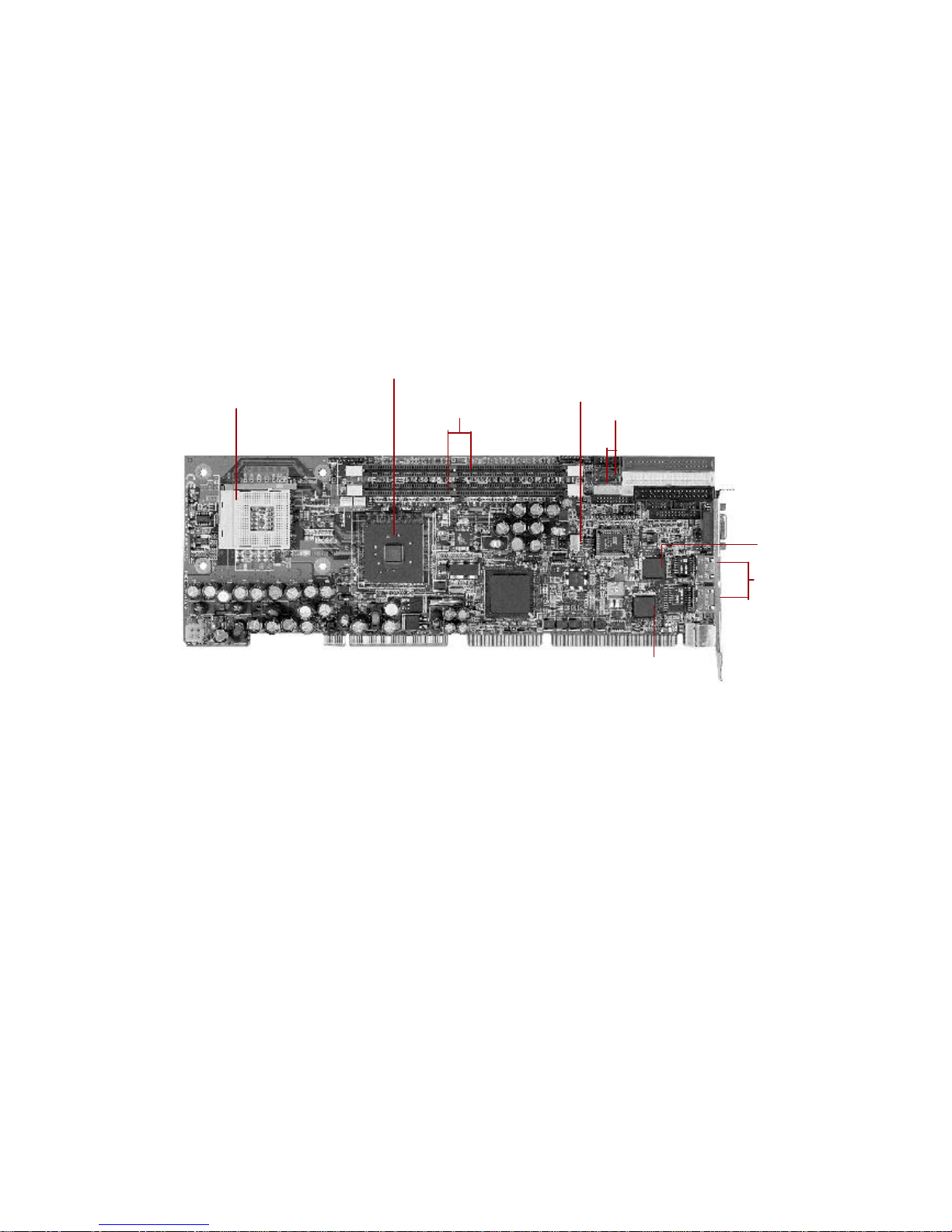
8
Figure 1-1: Peak735 Front Layout
1.3 Board Layout
I
Intel 82547EI Gigabit/CSA
Ethernet Controller or Intel
82562EX 10/100 LCI Ethernet
Controller
Dual LAN
Intel 82551QM
10/100 Ethernet
Controller
Serial ATA Connector x 2
ATX 5V Standby
Power Connector
Intel865G Chipset
w/integrated VGA
Controller
Socket 478 Intel Pentium 4 processor
up to 3.2GHz+ with 800MHz FSB
Max2GB DDR 400/Dual
Channel Memory in 2
DIMM Slots
Page 10
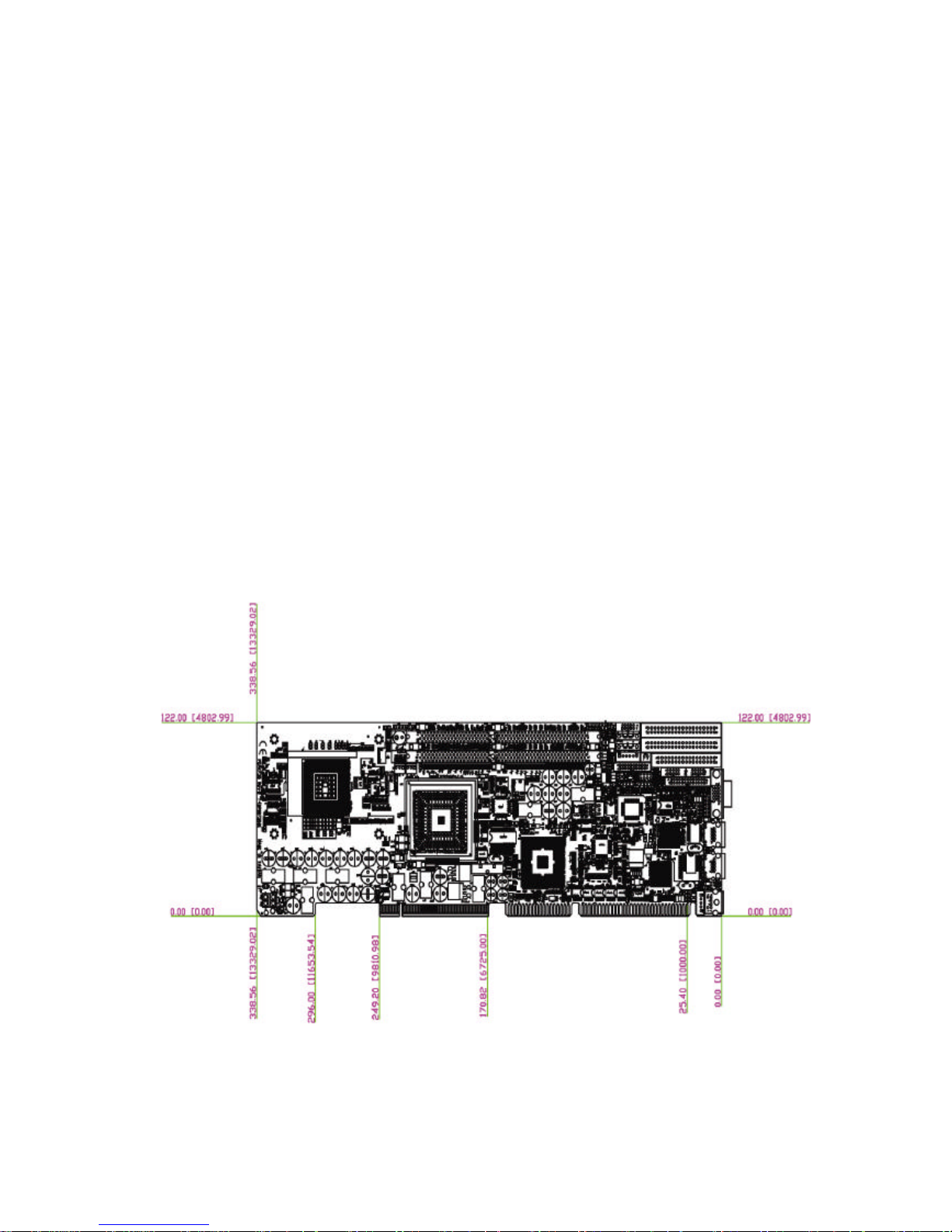
1.4 Checklist
After opening the package of PEAK 715-HT Series, please check and make
sure you have all of the following items:
? One PEAK 735 serie s SBC
(A mecha nical drawing of this model is shown below.)
? One PEAK 735 Quick R eference Guide
? One 50CM Cable JST 2.5mm 3 pin to 3 pin (5V standby ATX Power-on
Cable)
? One Y Cable for K eyboard and M ouse
? One 180 mm AU X Power Cable (for J2)
? One Cable Set (FDD x1, S IO+PIO x1, SIO x1/Keyboard x1/IDE66 x1)
? One U SB Cable with Bracket
? One Driver / M anual CD
Figure 1-1 : M echanical Drawing of PEAK 735 Series
9
Page 11

10
Chapter 2
Jumper & Switch Settings
Page 12

This chapter of the User’s Manual describes how to set jumpers.
Note: The procedures that follow are generic for all of the PEAK735 models
Before You Begin
Ensure you have a stable, clean working environment. Dust and dirt can get into components and cause a
malfunction. Use containers to keep small components separated.
Adequate lighting and proper tools can prevent you from accidentally damaging the internal components.
Most of the procedures that follow require only a few simple tools, including the following:
? A Philips screwdriver
? A flat-t ipped screwdriver
? A set of jewelers Screwdrivers
? A grounding strap
? An anti-static pad
Using your fingers can disconnect most of the connections. It is recommended that you do not use needlenosed pliers to disconnect connections as these can damage the soft metal or plastic parts of the
connectors.
Before working on internal components, make sure that the power is off. Ground yourself before touching any
internal components, by touching a metal object. Static electricity can damage many of the electronic
components. Humid environment tend to have less static electricity than dry environments. A grounding
strap is warranted whenever danger of static electricity exists.
Precautions
Computer components and electronic circuit boards can be damaged by discharges of static electricity.
Working on the computers that are still connected to a power supply can be extremely dangerous. Follow
the guidelines below to avoid damage to your computer or yourself.
??Always disconnect the unit from the power outlet whenever you are working inside the case.
??If possible, wear a grounded wrist strap when you are working inside the computer case. Alternatively,
discharge any static electricity by touching the bare metal chassis of the unit case, or the bare metal
body of any other grounded appliance.
??Hold electronic circuit boards (such as the PEAK639VL board) by the edges only. Do not touch the
components on the board unless it is nec essary to do so. Don’t flex or stress the circuit board.
??Leave all components inside the static-proof packaging that they shipped with until they are ready for
installation.
??Use correct screws and do not over tighten screws.
11
Page 13

2.1 Functions of Jumpers
You can use jumpers to set configuration options. The table below defines
function of each jumper:
12
Connector
Function
J1 AC'97
J2 Primary IDE
J3 SATA 0
J4 Secondary IDE
J5
SATA 1
J6 USB 2.0 Connector
J7 USB Exernal Power Connector
J8 Floppy
J9
DVI Connector(optional)
J10 CPU Fan
J11 System Fan
J12 COM1
J13
COM2
J14 PIO
J15 ATX Connector
J16 External Keyboard
JP2 Speaker
JP4
IDE LED
JP7 GPI/O Port
JP8 Keylock/Power LED
JP9 IR Connector
JP10
82551 LAN Speed 100 LED
JP11 82551 LAN ACT/LINK LED
JP12 ATX Push Button
JP13 82747/82562 LAN speed 100 LED
JP16
82747 LAN speed 1000 LED
JP17
Reset
JP18 82747/82562 LAN ACT/LINK LED
JP20
SMBUS
CON1 VGA Connector
CON2
82551 LAN Connector
CON3
82547/82562 LAN Connector
CON4 AUX+12V Power Connector
CON5
Keyboard+Mouse Connector
Table 2-1: Functions of Jumpers
Page 14
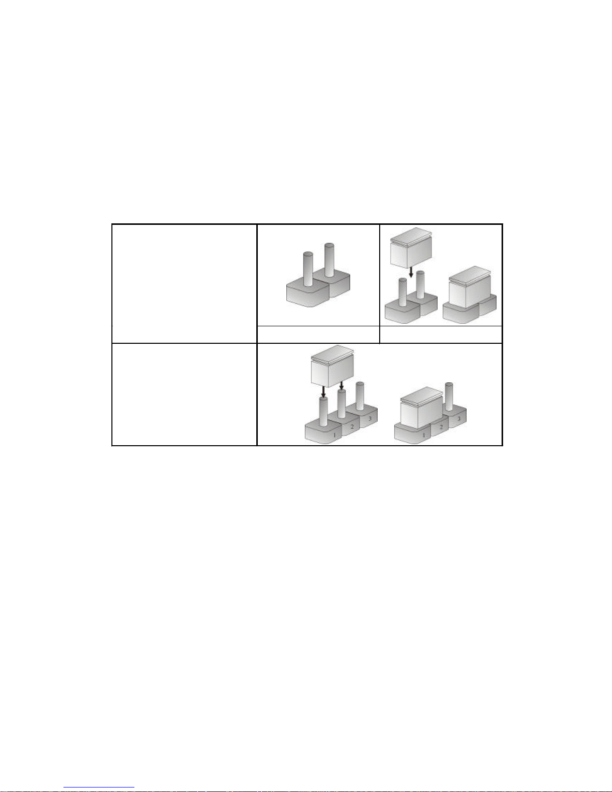
2.2 Setting Jumpers
A jumper is the simplest kind of electric switch. It consists of two metal pins and a
cap. When setting the jumpers, ensure that the jumper caps are placed on the
correct pins. When the jumper cap is placed on both pins, the jumper is SHORT.
If you remove the jumper cap, or place the jumper cap on just one pin, the jumpr is
OPEN. Please see the following illustrations:
Figure 2-1 : H ow to Set Jumpers
13
The illustrations on the right show
a 2-pin jumper. When the jumper
cap is placed on both pins, the
jumper is
SHORT
. If you remove
the jumper cap, or place the
jumper cap on just one pin, the
jumper is
OPEN
. Open (Off) Short (On)
These illustratio ns show a 3-pin
jumper. Pins 1 and 2 are SHORT.
Page 15
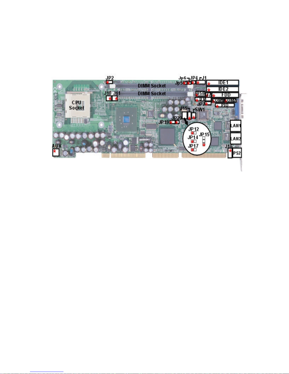
2.3 Location of Jumpers
The illustration below shows the location of the mainboard jumpers:
Figure 2-2 : Location of Jumpers
14
*
= Pin 1
Page 16

2.4 Jumper Setting
Switch Setting Table (* = default setup)
15
Device Select
SW1.1 SW1.2 SW1.3 SW1.4
ON Board LAN 82551 Enable *ON ON X OFF
ON Board LAN 82551 Disable OFF ON X OFF
ON Board TMDS Enable X ON * ON OFF
ON Board TMDS Disable X ON OFF OFF
DDR VDDQ Select
*2.5V 2.6V 2.7V 2.8V
JP5 *OFF ON OFF ON
JP6 *OFF OFF ON ON
AT/ATX Power model Select
AT ATX
JP15 *1-2 2-3
JP14 *1-2
RTC Clear
NORMAL Clear CMOS
JP19 *1-2 2-3
Page 17
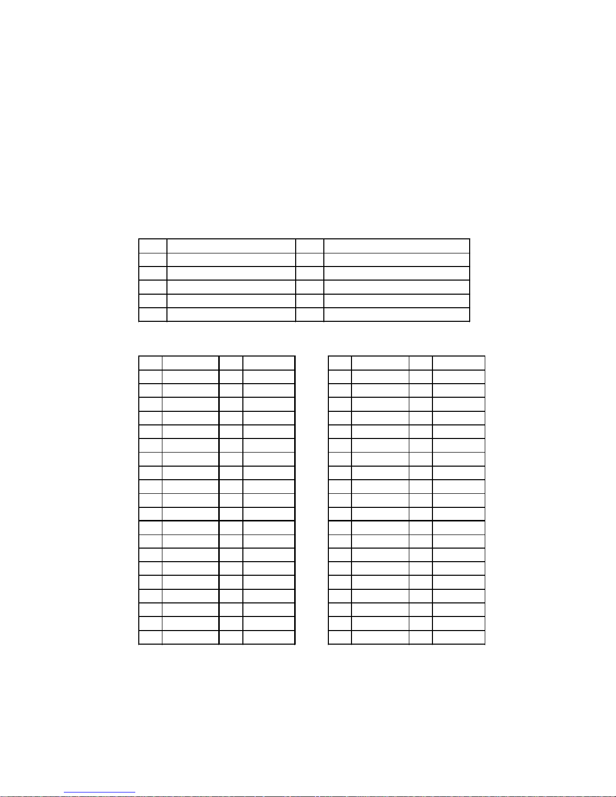
16
AC’97 connector
Pin Definition Pin Definition
1 AC_SDOUT_R 2 +5V
3 AC_RST# 4 GND
5 AC_SYNC 6 +12V
7 AC_SDIN0 8 AC_SDIN1_R
9 AC_BTCLK 10 AC_SDIN2_R
J2/J4: IDE connector
Pin Definition Pin Definition
Pin Definition Pin Definition
1 IDRST# 2 GND 1 IDRST# 2 GND
3 PDD7A 4 PD D8A 3 SD D7A 4 SDD8A
5 PDD6A 6 PDD9A 5 SD D6A 6 SDD9A
7 PDD5A 8 PDD710A 7 SD D5A 8 SDD710A
9 PDD4A 10 PD D711A 9 SD D4A 10 SDD711A
11 PDD3A 12 PDD712A 11 SDD3A 12 SDD712A
13 PDD2A 14 PDD713A 13 SD D2A 14 SDD713A
15 PDD1A 16 PDD714A 15 SD D1A 16 SDD714A
17 PDD0A 18 PDD715A 17 SD D0A 18 SDD715A
19 GND 20 NC 19 GND 20 NC
21 PDREQA 22 GND 21 SD REQA 22 GND
23 PDIOW#A 24 GND 23 SDIOW#A 24 GND
25 PDIOR#A 26 GND 25 SDIOR#A 26 GND
27 PIORDYA 28 IDE-PD1 27 SIO RDY A 28 IDE-PD2
29 PDDACK#A 30 GND 29 SDDACK#A 30 GND
31 HDIRQ14 32 NC 31 HDIRQ14 32 NC
33 PDA1A 34 P66 DET 33 PD A1A 34 S66 DET
35 PDA0A 36 PDA2A 35 S DA0A 36 SDA2A
37 PDCS#1 38 PDCS#3 37 SD CS#1 38 SDCS#3
39 IDEACTP# 40 GND
39 IDEACTP# 40 GND
2.5 Connector Pin Definition
Page 18

J3/J5:SATA connector
Pin Definition Pin Definition
1 GND 2 SATA0TXPC
4 GND 3 SATA0TXNC
7 GND 5 SATA0RXNC
6 SATA0RXPC
Pin Definition Pin Definition
1 GND 2 SATA1TXPC
4 GND 3 SATA1TXNC
7 GND 5 SATA1RXNC
6 SATA1RXPC
J6:USB connector
Pin Definition Pin Definition
1 +5VSBY 2 DATA03 DATA0+ 4 DATA15 DATA1+ 6 GND
J7:USB External Power connector
Pin Definition Pin Definition
1 +5VSBY 2 GND
J8:FDD connector
Pin Definition Pin Definition
1 GND 2 DENSEL#
3 GND 4 NC
5 GND 6 NC
7 GND 8 INDEX#
9 GND 10 MOTEA#
11 GND 12 DRVB#
13 GND 14 DRVA#
15 GND 16 MOTEB#
17 GND 18 DIR#
19 GND 20 STEP#
21 GND 22 WDATA#
23 GND 24 WGATE#
25 GND 26 TK00#
27 GND 28 WPT#
29 GND 30 RDATA#
31 GND 32 SIDE1#
33 GND 34 DSKCHG#
17
Page 19

J9:TMDS DVI connector
Pin Definition Pin Definition
1 TMDS_TX2N 2 TMDS_TX2P
3 GND 4 TMDS_TX1N
5 TMDS_TX1P 6 GND
7 +5V 8 GND
9 HotPlugDet 10 TMDS_TX0N
11 TMDS_TX0P 12 GND
13 TMDS_TXCP 14 TMDS_TXCN
15 GND 16 GND
17 DVICLK 18 DVIDATA
19 NC 20 NC
J10/J11:CPU FAN & SYSTEM FAN connector
Pin Definition Pin Definition
1 GND 2 +12V
3 SENSE
J12/J13: COM1/COM2
Pin Definition Pin Definitio
n
Pin Definition Pin Definitio
n
1 BDCD1# 2 BRXD1
1 BDCD2#
2 BRXD2
3 BTXD1 4 BDTR1#
3 BTXD2 4 BDTR2#
5 GND 6 BDSR1#
5 GND 6 BDSR2#
7 BRTS1# 8 BCTS1#
7 BRTS2# 8 BCTS2#
9 BRI1# 10 GND
9 BRI2# 10 GND
J14: PIO connector
Pin Definition Pin Definition
1 P_STB# 14 P_AFD#
2 P_PD0 15 P_ERR#
3 P_PD1 16 P_PINIT#
4 P_PD2 17 P_SLIN#
5 P_PD3 18 GND
6 P_PD4 19 GND
7 P_PD5 20 GND
8 P_PD6 21 GND
9 P_PD7 22 GND
10 P_ACK# 23 GND
11 P_BUSY 24 GND
12 P_PE 25 GND
13 P_SLCT 26 GND
J15:ATX POWER-ON connector
Pin Definition Pin Definition
1 +5VSBY 2 GND
3 PSON#
18
Page 20
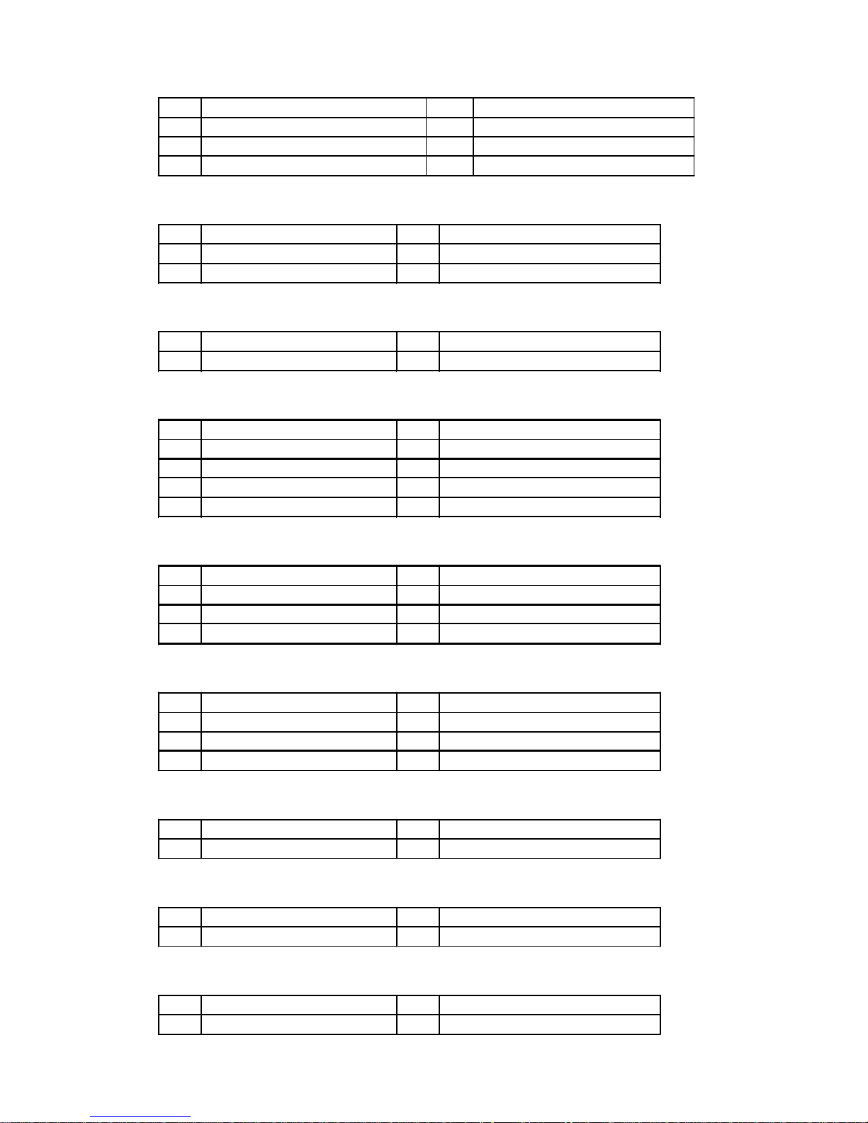
J16:External Keyboard
Pin Definition Pin Definition
1 KBCLK 2 KBDATA
3 NC 4 GND
5 +5V
JP2:SPEAKER External connector
Pin Definition Pin Definition
1 SPEAKERR# 2 GND
3 GND 4 +5V
JP4:IDE Active LED connector
Pin Definition Pin Definition
1 +5V 2 IDE_LED
JP7:GPIO connector
Pin Definition Pin Definition
1 GP27_D_IN1 ( PIN20 ) 2 GP23_D_OUT 1 ( PIN24 )
3 GP26_D_IN2 ( PIN21 ) 4 GP22_D_OUT 2 ( PIN25 )
5 GP25_D_IN3 ( PIN22 ) 6 GP21_D_OUT 3 ( PIN26 )
7 GP24_D_IN4 ( PIN23 ) 8 GP20_D_OUT 4 ( PIN27 )
JP8:Keylock/Power LED connector
Pin Definition Pin Definition
1 +5V Pull-up (Power LED) 2 N.C
3 GND (Power LED) 4 Keylock
5 GND (Key Lock)
JP9:IR connector
Pin Definition Pin Definition
1 +5V 2 CIRRX
3 RIRX 4 GND
5 IRTX
JP10:82551QM LAN External SPEED LED connector
P in Definition Pin Definition
1 +3VSBY 2 SPEED_LAN
JP11:SMBUS External connector
Pin Definition Pin Definition
1 SMBCLK 2 SMBDATA
JP12:ATX Push Button connector
Pin Definition Pin Definition
1 GND 2 PWRBT#
19
Page 21

JP13:82747EI/82562EX LAN External SPEED 100 LED connector
Pin Definition Pin Definition
1 +3VSBY 2 LINK100
JP16:82747EI LAN External SPEED 1000 LED connector
Pin Definition Pin Definition
1 +3VSBY 2 LINK1000
JP17:Hardware Reset connector
Pin Definition Pin Definition
1 RESET 2 GND
JP18: 82747EI/82562EX LAN External ACTIVE&LINK LED connector
Pin Definition Pin Definition
1 LINK_UP 2 ACTIVITY
JP20:SMBUS connector
Pin Definition Pin Definition
1 SMBCLK 2 SMBDATA
CON1:VGA connector
Pin Definition Pin Definition
1 RED 2 GREEN
3 BLUE 4 NC
5 GND 6 GND
7 GND 8 GND
9 +5V 10 GND
11 NC 12 DDCDAT
13 HSYNC 14 VSYNC
15 DDCCLK
CON2:82551 RJ45 connector
Pin Definition Pin Definition
1 LAN1_TXP 2 LAN1_TXN
3 LAN1_RXP 4 TERMPLANE
5 TERMPLANE 6 LAN1_RXN
7 TERMPLANE 8 TERMPLANE
9 SPEED_LAN1 10 +3VSBY
11 LILED_LAN1 12 ACTLED_LAN1
20
Page 22

CON3:82547/82562 RJ45 connector
Pin Definition Pin Definition
1 LAN2_MDX_0P_TX P 2 LAN2_MDX_0N_TXN
3 LAN2_MDX_1P_RX P 4 LAN2_MDX_2P
5 LAN2_MDX_2N 6 LAN2_MDX_1N_RXN
7 LAN2_MDX_3P 8 LAN2_MDX_3N
9 LAN2_LINK1000 10 +3VSBY
11 LAN2_LINK_UP 12 LAN2_ACTIVITY
CON4: AUX +12V Power Connector
Pin Definition Pin Definition
1 GND 2 GND
3 +12V 4 +12V
CON5: Key board + mouse connector
Pin Definition Pin Definition
1 KBDATA 2 MOUSEDATA
3 GND 4 +5V
5 KBCLK 6 MOUSECLK
21
Page 23

Chapter 3
Expanded Capabilities
22
Page 24

3.1 System Memory
Your system memory is provided by DIMM’s (Dual In-line Memory Modules) on the
CPU board. The CPU board contains two memory banks: Bank 0 and 1, corresponds to connector DIMM1, DIMM2.
The table below shows possible DIMM configurations for the memory banks.
Please be noted that the PEAK 735 Series supports Double Data (DDR333)
SDRAM. Configurations using different brands of memory modules are not
recommended.
DIMM 1 DIMM2 Total Memory
128MB Empty 128MB
Empty 128MB 128MB
128MB 128MB 256MB
256MB Empty 256MB
Empty 256MB 256MB
256MB 256MB 512MB
512MB Empty 512MB
Empty 512MB 512MB
512MB 512MB 1024MB
1024MB Empty 1024MB
Empty 1024MB 1024MB
1024MB 1024MB 2048MB
23
Table 3-1 : PEAK 735 Serie s DIMM Configurations
Page 25
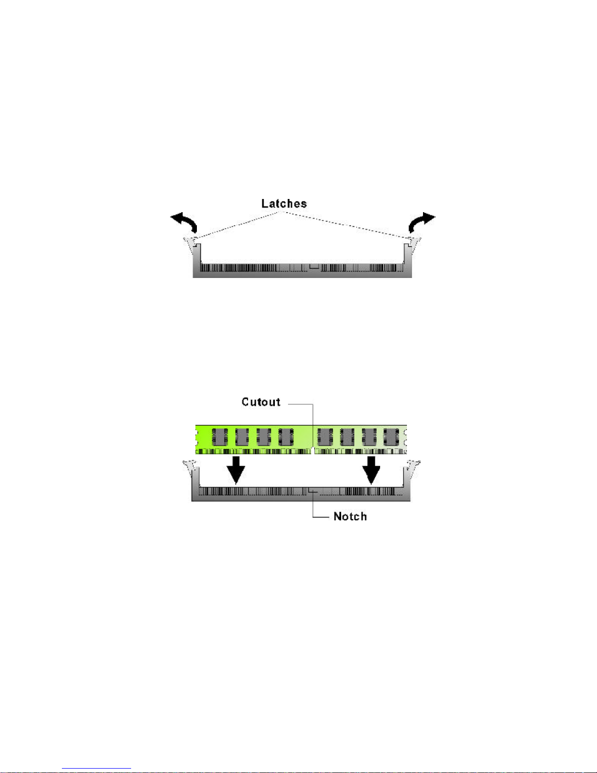
3.2 Installing DIMM
To install DIMM:
1. Make sure the two handles of the DIMM sockets are in the “open” position, i.e.
the handles stay outward.
Figure 3-1 : How to Install DIMM (1)
2. Slowly slide the DIMM modules along the plastic guides in the both ends of the
socket.
Figure 3-2 : H ow to Install DIMM (2)
24
Page 26
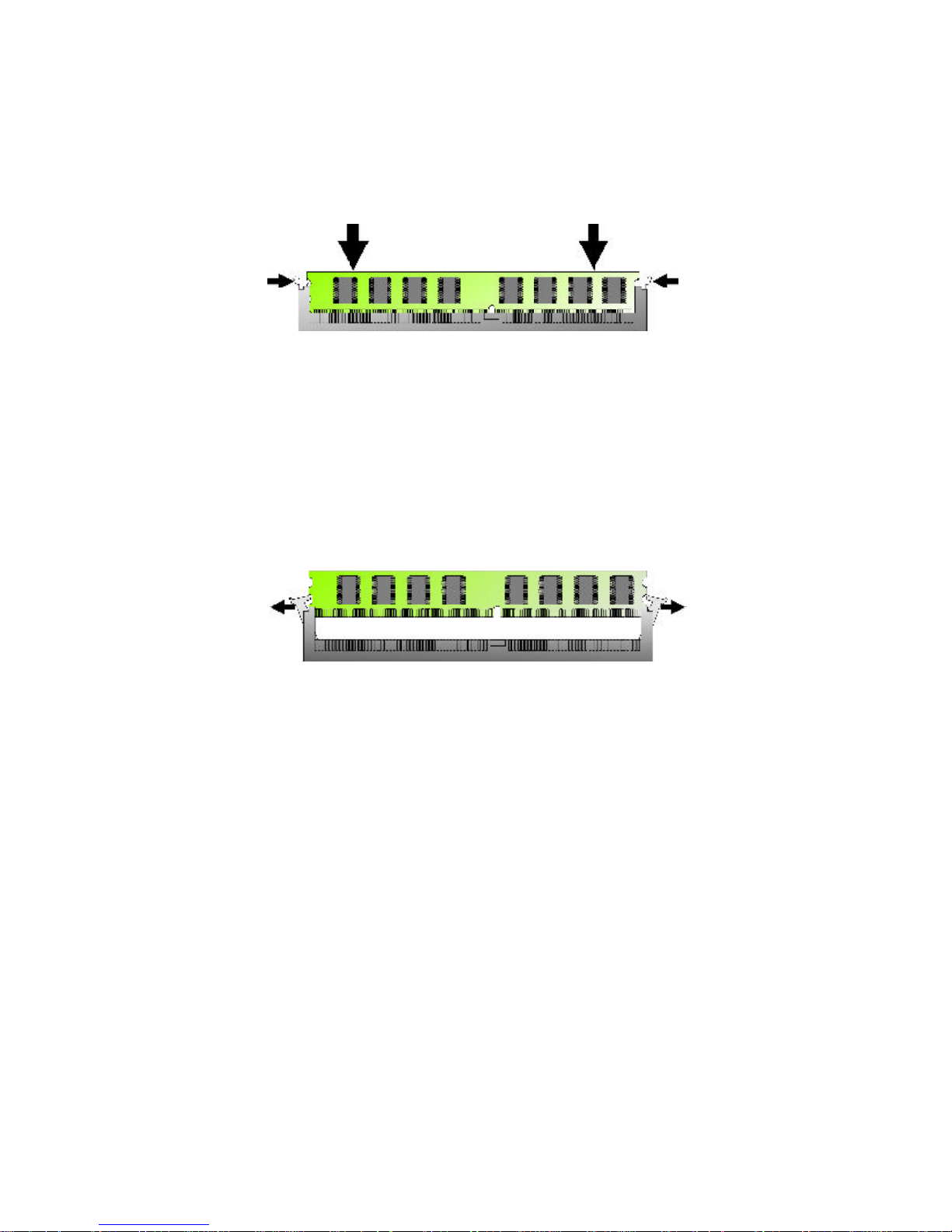
3. Then press the DIMM module down right into the socket, until a click is heard.
That means the two handles automatically locked the memory modules into the
right position of the DIMM socket.
4. To take away the memory module, just push the both handles outward, the
memory module will be ejected by the mechanism in the socket.
Figure 3-3 : H ow to Install DIMM (3)
Figure 3-4 : How to Install DIM M (4)
25
Page 27
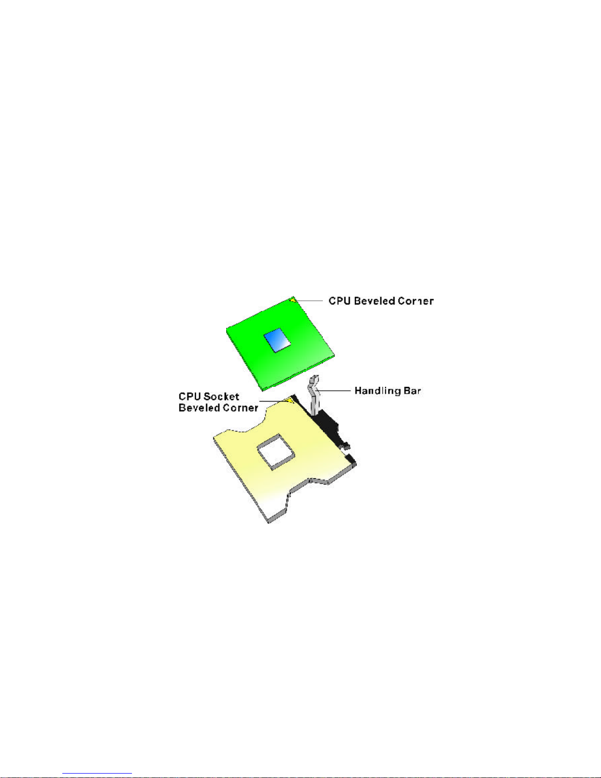
3.3 Changing CPU
To change the CPU:
1. Pull the handling bar of the socket upward to the other end to loosen the
socket’s openings. Carefully lift the existing CPU up to remove it from the socket.
2. Place the new CPU on the middle of the socket, orienting its beveled corner to
line up with the socket’s beveled corner. Make sure the pins of the CPU fit evenly
to the socket openings. Replace the handling bar to fasten the CPU to the socket.
Figure 3-5 : How to Change CPU
26
Page 28

3.4 Installing the Fan Heatsink
Use the following instructions for installing the fan heatsink:
1. The heatsink has thermal interface material attached to the bottom, shown in
Figure 3-7. Be careful not to damage the thermal interface material.
2. Align the fan heatsink and clip assembly (A in Figure 3-6) with the retention
mechanism (the fan heatsink is symmetrical) and place it on the processor (as
shown in Figure 3-7). Allow the heatsink base to compress (without rotating or
twisting) the thermal interface material over the surface of the processor's integrated heat spreader.
3. With the clip levers (C in Figure 3-6) in the upward position, push down on all
four clip frame corners (D in Figure 3-6) to secure the clip frame latches (E in
Figure 3-6) to the retention mechanism hooks (F in Figure 3-6), as shown in Figure
3-8.
Note: Make sure the processor fan cable is free from any obstruction and is not
trapped under clip frame (B in Figure 3-6).
4. Note: It is important to not allow the heatsink to rotate or twist on the
processor's integrated heat spreader. Securing the fan heatsink while closing the
clip levers will ensure the thermal interface material is not damaged and the processor will operate correctly. Follow these steps, for closing the clip levers and
ensuring the thermal interface material is not damaged:
a. ) Make sure to close the clips levers in opposing directions, one at a time
(levers require force to be completely closed), as shown in Figure 3-9a. First, close
the clip lever (1 in Figure 3-9b), while holding the topside of the fan heatsink with
your other hand (A in Figure 3-9b).
b. ) Then, close the clip lever (2 in Figure 3-9c), while holding the topside of the
fan heatsink with your other hand (B in Figure 3-9c).
5. Once the clip levers are closed, verify that the heatsink is securely retained and
that the clip frame latches are properly engaged with the retention mechanism
hooks.
Note: When installed, the fan heatsink and clip assembly may cause the
motherboard to slightly bend or flex. This provides the proper mechanical support
for the processor (with attached fan heatsink and clip assembly) and helps prevent
against damage during system shipment.
27
Page 29
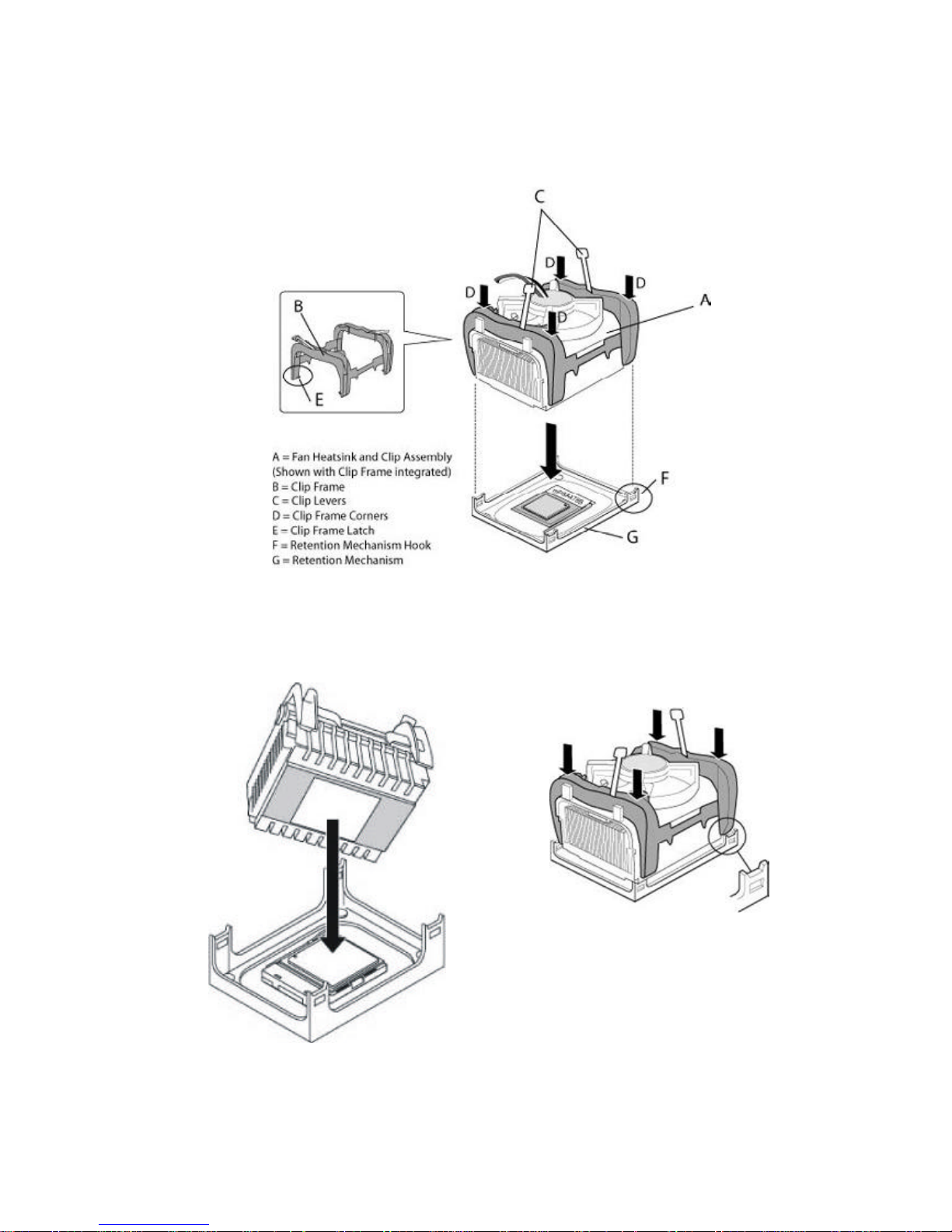
6. Lastly, connect the processor fan cable to the motherboard fan power header
(Figure 3-10). Consult the motherboard manual to determine the correct fan
header to use.
Fa n Heatsink and Clip Assembly Terminology
Align Fan H eatsink and Clip Assembly
Figure 3-8: Installing the Fan Heatsink (3)
Push Down Clip Frame
Corners to Secure to R etention
M echanism Hooks
Figure 3-6: Installing the Fan Heatsink (1)
Figure 3-7: Installing the Fan H eatsink (2)
28
Page 30
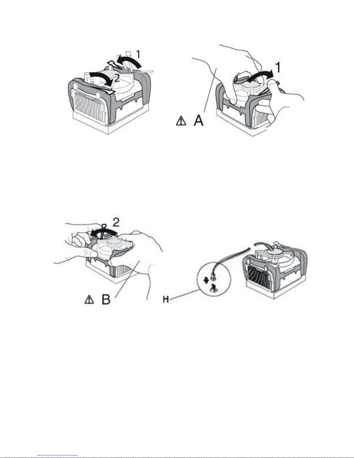
29
Figure 3-9a: Installing the Fan Figure 3-9b: Installing the Fan
H eatsink (4) Heatsink (5)
Close Clip Levers, Close Clip Lever (1),
One at a Time While H olding the Topside
of Fan Heatsink (A)
Figure 3-9c: Installing the Fan Figure 3-10: Installing the Fan
Heatsink (6) H eatsink (7)
Close Clip Lever (2), Connect Fan Cable to M otherboard
While H olding the Topside of
Fan H eatsink (B)
Page 31

On-Chip Serial ATA Setting
On-Chip Serial ATA
The setting is used to specify te SATA controller.
Settings:
Disable, Auto, Combined Mode, Enhanced Mode, SATA only
If <Combined Mode> is selected, PATA and SATA will be combined.
If <Enhanced Mode> is selected, PATA and SATA will both be enabled.
If <Auto> is selected, PATA and SATA will be arranged by BIOS, and you will be able to
see the IDE Device Status listed in the Standard CMOS Features.
Serial ATA Port O/I Mode
Select a compatible mode for Port 1 and Port 2 from the Award Setting to the Chipset
Setting:
Primary Master Compatible Mode w/Serial ATA Port 1 set to Primary Master
Primary Slave Primary Slave
Secondary Master Secondary Master
Secondary Slave Secondary Slave
Primary Master Compatible Mode w/only serial ATA Enabled and Port 1 set
to Primary Master
Secondary Master Secondary Master
SATA 1 Master Enhance mode w/Port 1 set to Native Mode Master
SATA2 Master Enhance mode w/Port2 set to Native Mode Master
30
Page 32

31
Chapter 4
Award BIOS Setup
Page 33

This chapter explains how to use the BIOS Setup program for the EBC572(A). The
current BIOS setup pictures in the chapter is for reference only, which may change by
the BIOS modification in the future. User can download any major updated items or
reversion from NEXCOM web site http://www.nexcom.com.tw. If any unclear message
occurs, please contact NEXCOM customer service representative for help or log onto
http://www.nexcom.com.tw/contact/contact.htm.
About the BIOS
The BIOS (Basic Input and Output System) Setup program is a menu driven utility that
enables you to make changes to the system configuration and tailor your system to
suit your individual work needs. It is a ROM-based configuration utility that displays the
system’s configuration status and provides you with a tool to set system parameters.
These parameters are stored in non-volatile battery-backed-up CMOS RAM that
saves this information even when the power is turned off. When the system is turned
back on, the system is configured with the values found in CMOS.
With easy-to-use pull down menus, you can configure such items as:
? Hard drives, diskette drives, and peripherals
? Video display type and display options
? Password protection from unauthorized use
? Power management features
When to Run BIOS
This program should be executed under the following conditions:
? When changing the system configuration
? When a configuration error is detected by the system and you are prompted to
make changes to the Setup program
? When resetting the system clock
? When setting the CPU clock speed so that it automatically runs either fast or slow
? When redefining the communication ports to prevent any conflicts
? When making changes to the Power Management configuration
? When changing the password or making other changes to the security setup
Normally, CMOS setup is needed when the system hardware is not consistent with the
information contained in the CMOS RAM, whenever the CMOS RAM has lost power,
or the system features need to be changed.
32
Page 34
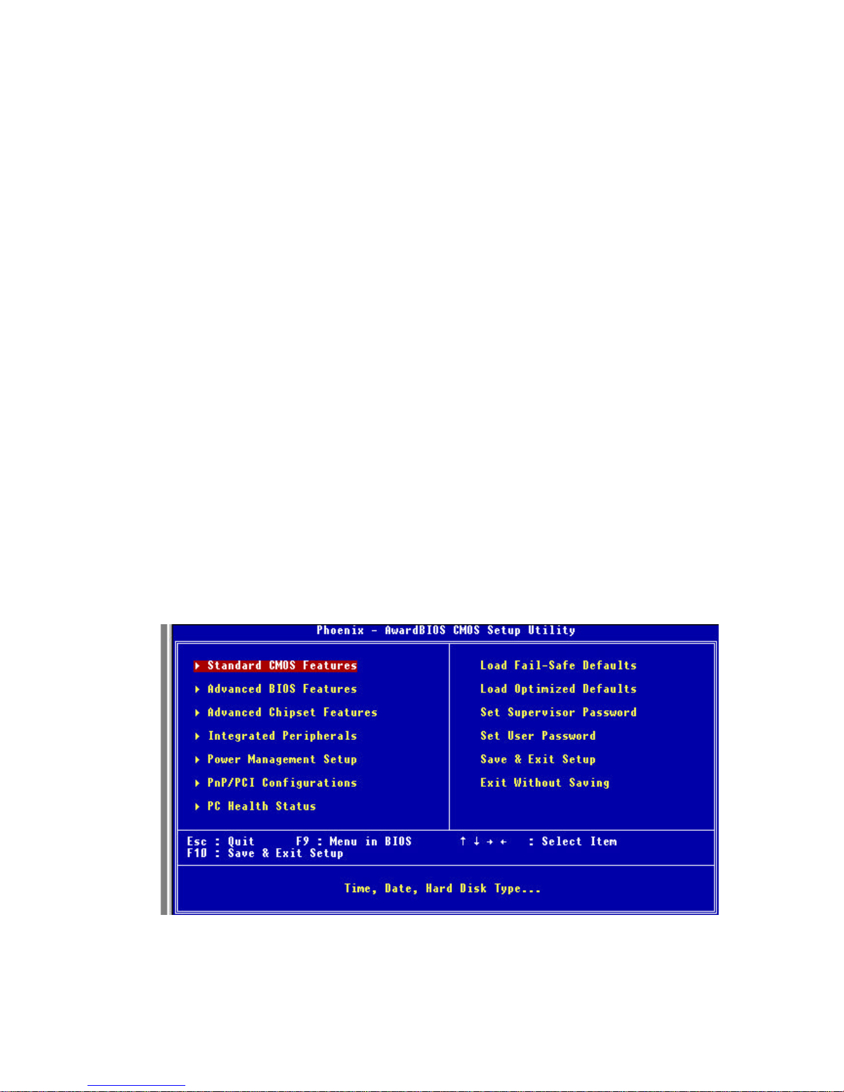
4.1 Entering Setup
When the system is powered on, the BIOS will enter the Power-On Self Test (POST)
routines. These routines perform various diagnostic checks; if an error is encountered,
the error will be reported in one of two different ways:
? If the error occurs before the display device is initialized, a series of beeps will be
transmitted.
? If the error occurs after the display device is initialized, the screen will display the
error message.
Powering on the computer and immediately pressing <Del> allows you to enter Setup.
Another way to enter Setup is to power on the computer and wait for the following
message during the POST:
TO ENTER SETUP BEFORE BOOT
PRESS <CTRL-AL T-ESC> OR <DEL> KEY
Press the <Del> key or press the <Ctrl>, <Alt>, and <Esc> keys to enter Setup:
4.2 The Main Menu
Once you enter Award BIOS CMOS Setup Utility, the Main Menu (Figure 1) will ap-
pear on the screen. The main menu allows you to select from ten setup functions and
two exit choices. Use arrow keys to select among the items and press<Enter> to
accept or enter the sub-menu.
Figure 4-1: BIOS Setup U tility Main M enu
33
Page 35

Advanced Chipset Features
Use this menu to change the values in the chipset registers and optimize the system’s
performance
Integrated Peripherals
Use this menu to specify your settings for integrated peripherals
Power Management Setup
Use this menu to specify your settings for power management.
PnP/PCI Configurations
This entry appears if your system supports Plug and Play and PCI Configuration
PC Health Status
Displays CPU, System Temperature, Fan Speed, and System Voltages Value
Load Fail-Safe Defaults
Use this menu to load the BIOS default values for the minimal/stable
performance for your system to operate.
Load Optimized Defaults
Use this menu to load the BIOS default values, i.e., factory settings
for optimal performance system operations. While Award has de-signed
the custom BIOS to maximize performance, the factory has
the option to change these defaults to meet their needs.
Set Supervisor/U ser Pa ssword
Enables you to change, set, or disable the supervisor or user pass-word.
34
Standard CMOS Features
Use this menu for basic system configuration
Advanced BIOS Features
Use this menu to set the Advanced Features available on the system
Page 36

Save & Exit Setup
Saves CMOS value changes to CMOS and exits setup.
Exit Without Saving
Ignores all CMOS value changes and exits setup.
4.3 Getting Help
Main Menu
The on-line description of the highlighted setup function is displayed at the bot-
tom of the screen.
Status Page Setup Menu/ Option Page Setup Menu
Press F1 to pop up a small help window that describes the appropriate keys
to use and the possible selections for the highlighted item. To exit the Help
Window press <F1> or <Esc>.
35
Page 37
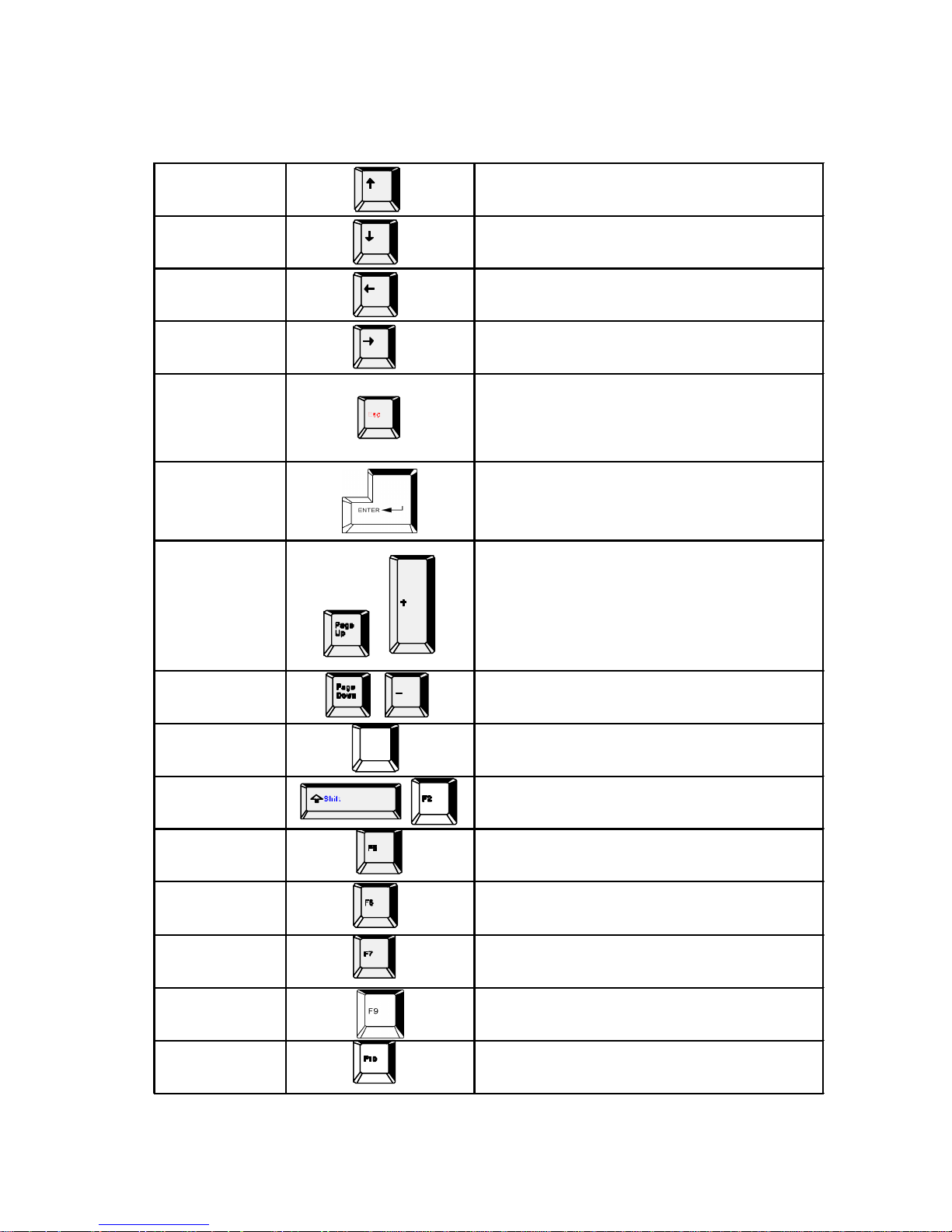
4.4 Control Keys
The table below lists the keys that help you navigate the setup program.
Figure 4-2 : BIOS Control Keys
36
Up arrow
Move to previous item
Down arrow
Move to next item
Left arrow
Move to the item to the left
Right arrow
Move to the item to the right
Esc key
Main Menu: Quit without saving changes to CMOS
Status/Option Page Setup Menus: Exit curre nt page and
r eturn to Main Menu.
Enter Key
Select or Accept an Item
PgUp/plus key
Increase the numeric value or make changes
PgDn/minus key
Decrease the numeric value or make changes
F1 key
F1
General help, only for Status Page Setup Menu and
Option Page Setup Menu
F2/Shift + F2 key
Change color from total 16 colors. F2 to select color
forward, (Shift) F2 to select color back ward
F5 key
Restore the previous CMOS value from CMOS (only
for O ption Page Setup Menu)
F6 key
Load the default CMOS value from BIOS default table
(only for Option Page Setup Menu)
F7 key
Load the Setup default value (only for Option Page
Setup Menu)
F9 Key
Menu in BIOS
F10 key
Save all the CMOS changes (only for Main Menu)
Page 38
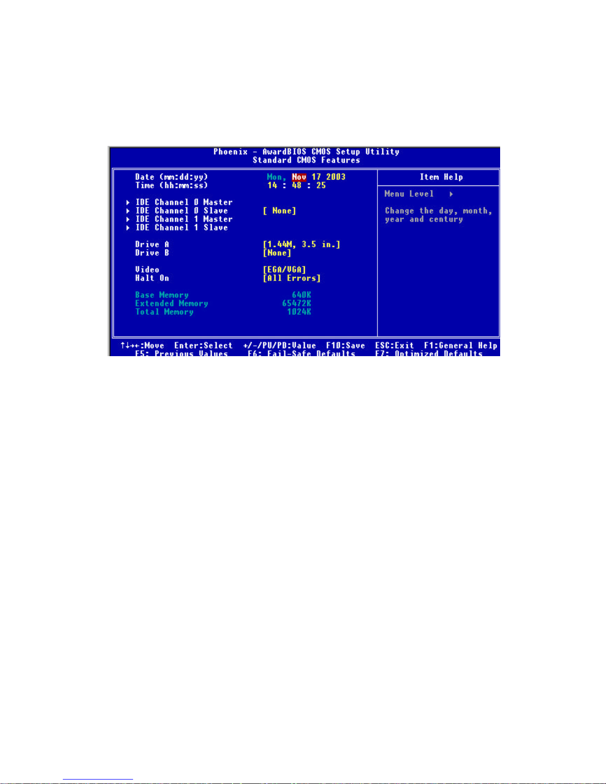
4.5 Standard CMOS Features
Selecting Standard CMOS Features on the main program screen displays the
following menu:
IDE Devices
Your computer has two IDE channels and each channel can be installed with one or two
devices (Master and Slave). Use these items to configure each device on the IDE
channel. Press <Enter> to display the IDE submenu:
The times format in <hour> <minute> <second>. The time is calculated based on the
24-hour military-time clock. For example, 1 p.m. is 13:00:00.
Figure 4-3 : BIOS -- Sta ndard CMOS Features
37
The Standard CMOS Setup utility is used to configure the following features:
Date (mm:dd:yy)
The BIOS determines the day of the week from the other data information. This field is
for information only. Press the left or right arrow key to move to the desired field (date,
month, year). Press the PgUp or PgDn key to arrange the setting, or type the desired
value into the field.
Time (hh:mm:ss)
Page 39
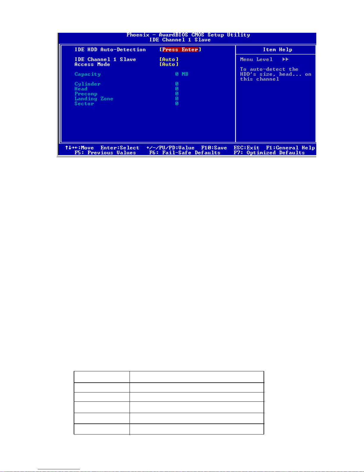
IDD HDD Auto-Detection
If you want the Setup Utility to automatically detect and configure a hard disk drive
on the IDE channel, press <Enter> while this item is highlighted.
If your system has an IDE hard drive, you can use this utility to detect its param-
eters and enter them into the Standard CMOS Setup automatically.
If the auto-detected parameters displayed do not match the ones that should be
used for your hard drive, do not accept them. Press the <N > key to reject the
values and enter the correct ones manually in the Standard CMOS Setup screen.
(N ote: If you are setting up a new hard disk drive that supports LBA mode, more
than one line will appear in the parameter box. Choose the line that lists LBA for an
LBA drive.)
Do not choose Large or N ormal if the hard disk drive is already fully formatted
when you installed it. Select the mode that was used to format it.
IDE Cha nnel Slave
If you leave this item at Auto, the system will automatically detect and configure
any IDE devices it finds. If it fails to find a hard disk, change the value to M anual
and then manually configure the drive by entering the characteristics of the drive in
the items below:
Capacity approximate hard disk drive capacity
Cylinder number of cylinders
Head number of heads
Precom p write precompensation cylinder
Landing Zone landing zone
Sector number of sectors
Figure 4-4 : BIOS -- IDE Cha nnel Slave
38
Page 40
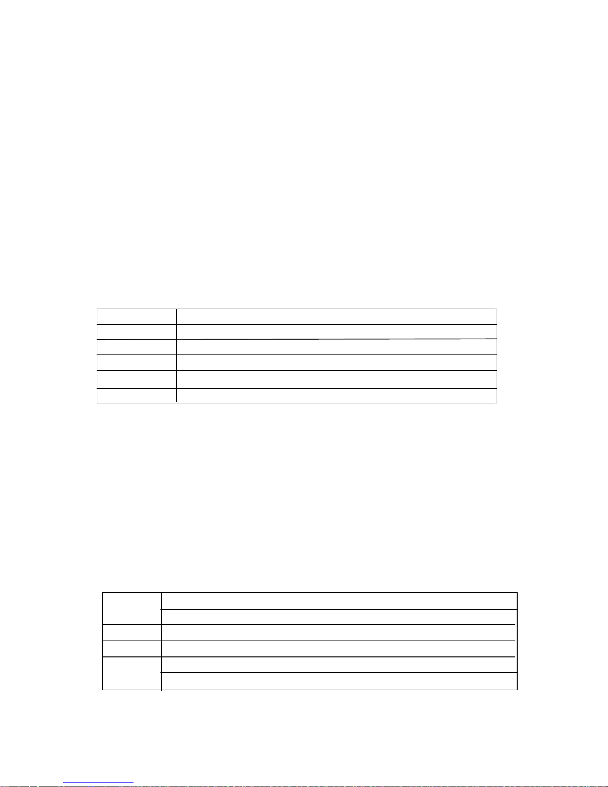
EGA /VGA Enhanced Graphics Adapter/Video Graphics Array. For EGA, VGA,
SEGA, or PGA monitor adapters.
CGA 40 Color Graphics Adapter, power up in 40 column mode
CGA 80 Color Graphics Adapter, power up in 40 column mode
Mono Monochrom e adapter, includes high resolution monochrome
adapters
39
Refer to your drive’s documentation or look on the drive if you need to obtain this
information. If no device is installed, change the value to N one.
Access M ode
This item defines some special ways that can be used to access IDE hard disks
such as LBA (Logical Block Addressing). Leave this value at Auto and the system
will automatically decide the fastest way to access the hard disk drive.
Press <Esc> to close the IDE device submenu and return to the Standard CMOS
Features page.
Floppy Drive A
Options for these fields are:
None No floppy drive installed
360K, 5.25 in 5-1/4 inch PC-type standard drive; 360 kilobyte capacity
1.2M, 5. 25 in 5-1/4 inch A T-type high- density drive; 1.2 m egabyte capacity
720K, 3.5 in 3-1/2 inch double-sided drive; 720 kilobyte capacity
1.44M, 3.5 in 3-1/2 inch double-sided drive; 1.44 megabyte capacity
2.88M, 3.5 in 3-1/2 inch double-sided drive; 2.88 megabyte capacity
The N one option could be used for diskless workstations.
Video
Set this field to the type of graphics card installed in your system. If you are using a
VGA or higher resolution card, choose the EGA/VGA option. The options are:
Page 41

H alt On
This setting determines which type of errors will cause the system to halt during
booting. The options are:
A ll Errors Whenever the BIOS detects a non-fatal error, the system
will be stopped and you will be prompted.
No Errors The system boot will not be stopped for any error that may
be detected.
A ll, But Keyboard The system boot will not stop for a ke yboard error; it will
stop for all other errors.
A ll, But Diskette The system boot will not stop for a disk error; it will stop
for all other errors.
A ll, But Disk/Key The system boot will not stop for a keyboard or disk error; it
will stop for all other errors.
Ba se/Extended/Total Memory
This category is display-only. The contents are determined by the POST (Power-On
Self-Test) of the BIOS. You cannot make changes to these fields.
Ba se Memory: Also called conventional memory. The DOS operating system and
conventional applications use this area.
Extended M emory: The POST of the BIOS will determine the amount of extended
memory installed in the system.
Total M emory: This option shows system memory capacity.
After you have made your selections in the Standard CMOS Setup screen, press
<ESC> to go back to the main screen.
40
Page 42
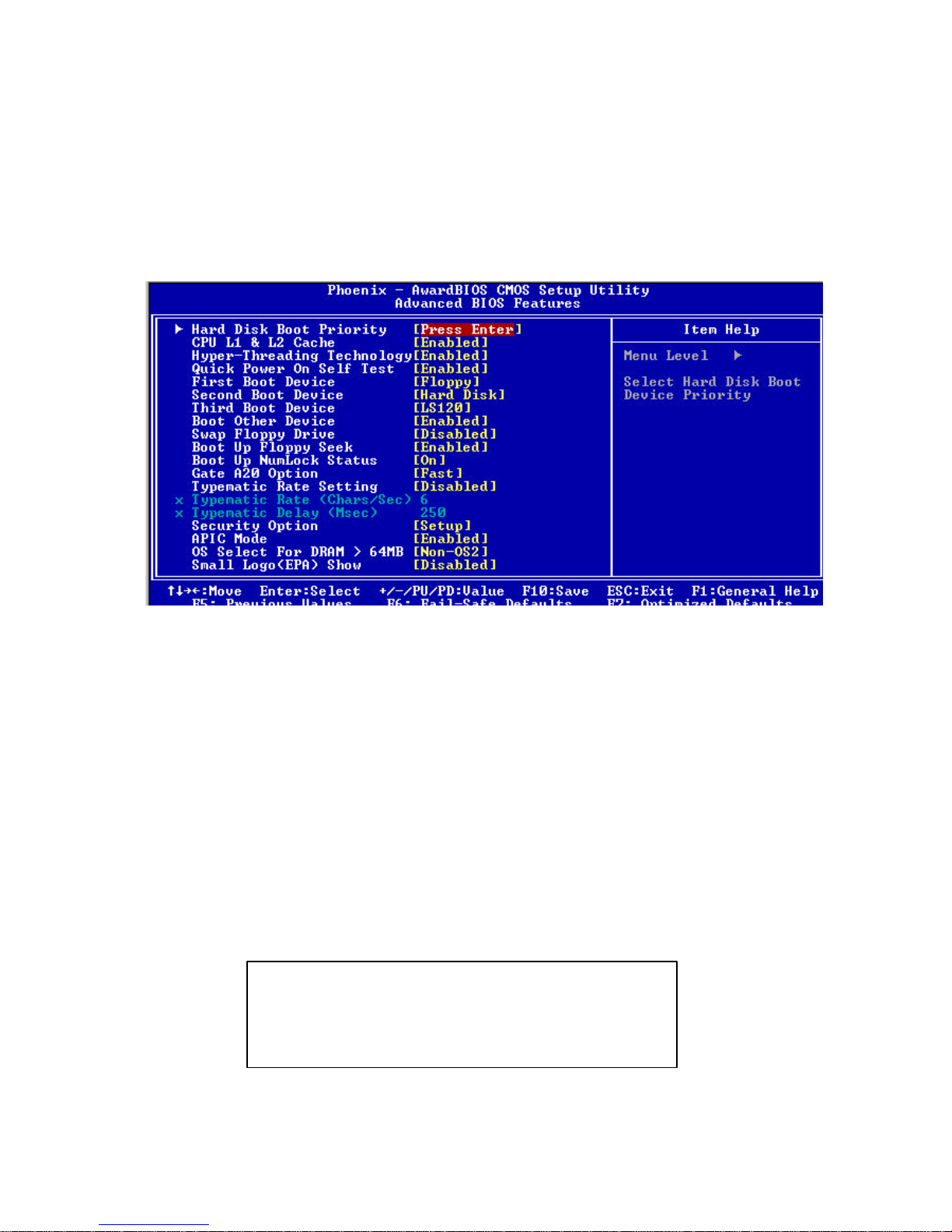
4.6 Advanced BIOS Features
Selecting Advanced BIOS Features on the main program screen displays this
menu, which allows you to define advanced information about your system. You
can make modifications to most of these items without causing fatal errors to your
system.
Figure 4-5 : BIOS -- Advanced BIOS Features
The following explains the options for each feature:
H ard Disk Boot Priority:
Press <Enter> to enter a sub menu which shows every current hard drive installed.
Use <PageUp> or <PageDown> key to select the first boot hard disk.
Virus Warning
Allows you to choose the Virus Warning feature for IDE Hard Disk boot sector
protection. If this function is enabled and someone attempts to write data into this
area, BIOS will show a warning message on screen and an alarm will beep.
· Enabled: Activates automatically when the system boots up causing the follow-
ing warning message to appear when anything attempts to access the boot sector
or hard disk partition table:
! WARNING!
Disk boot sector is to be modified
Type “Y” to accept write or “N” to abort write
Award Software, Inc.
· Disable d: No warning message will appear when an attempt is made to access
the boot sector or hard disk partition table.
41
Page 43

Note:
This function is available only for DOS and other operating systems that do not trap
INT13. For complete protection against viruses, install virus software in your operating
system and update the virus definitions regularly. Many disk diagnostic programs
that access the boot sector table can trigger the virus warning message. If you plan
to run such a program, we recommend that you disable the virus warning.
CPU L1 & L2 Cache
Cache memory is additional memory that is much faster than conventional DRAM
(system memory). This BIOS feature is used to enable or disable the processor's
Level 1 and Level 2 cache. Naturally, the default and recommended setting is Enabled.
H yper Thre ading Technology
The Intel Hyper-Threading Technology allows a single processor to execute two or
more separate threads concurrently. When hyper-threading is enabled, multi-
threaded software applications can execute their threads in parallel, thereby im-
proving the processor’s performance.
Quick Power On Self Te st
This item speeds up the Power On Self Test (POST) when you turn on the
computer. If it is set to Enabled, BIOS will shorten or skip some check items dur-
ing the POST.
First/Second/Third Boot Device
BIOS attempts to load the operating system from the devices in the sequence
selected in these items. The available choices are Floppy, LS120, Hard Disk
CDROM, ZIP100, USB-FDD, USB-CDROM, LAN, Disabled.
Boot Other Device
If the selected boot devices fail to boot, selecting Enabled for this item allows the
BIOS to boot from other boot devices (in a predefined sequence) which are
present but not selected as boot devices in the setup.
Swa p Floppy drive
If the system has two floppy drives, use this item to swap the logical drive name
assignments.
42
Page 44

Boot U p Floppy Seek
Enable this to allow the system to search for floppy drives during the POST. Dis-able
this item to boot faster.
Boot U p NumLock Status
Toggle between On or Off to control the state of the NumLock key when the system
boot. If On, the numeric keypad is in numeric mode. If Off, the numeric keypad is in
cursor control mode.
Gate A20 Option
Enables you to select whether the chipset or the keyboard controller should control
Gate A20. The options are:
· N ormal: A pin in the keyboard controller controls Gate A20.
· Fast: Lets chipset control Gate A20.
Type matic Rate Setting
If set to Enabled, enables you to set the Typematic Rate and Typematic Delay.
Type matic Rate (Chars/Sec)
This setting controls the speed at which the system registers held-down key-
strokes. The choices range from 6 to 30 Chars/Sec.
Type matic Delay (Msec)
This setting controls the time between the display of the first character and suc-
cessive characters. There are four delay choices: 250ms, 500ms, 750ms and
1000ms.
S ecurity Option
Enables you to select whether the password is required every time the system
boots or only when you enter Setup.
System: The system will not boot and access to Setup will be denied if the
correct password is not entered at the prompt.
Setup: The system will boot, but access to Setup will be denied if the correct
password is not entered at setup.
APIC M ode
43
Page 45

The APIC Mode BIOS feature is used to enable or disable the motherboard’s APIC
(Advanced Programmable Interrupt Controller). If your single-processor motherboard
supports APIC and you are using a Win32 operating system (Windows NT, 2000 and
XP), it’s recommended that you enable this feature to allow faster and better IRQ
handling. If you are using a multiprocessor motherboard, you must enable this feature
because it’s required for IRQ handling in multiprocessor systems.
OS Select for DR AM > 64MB
Set to OS2 if the system memory size is greater than 64 MB and the operating
system is OS/2.
44
Page 46
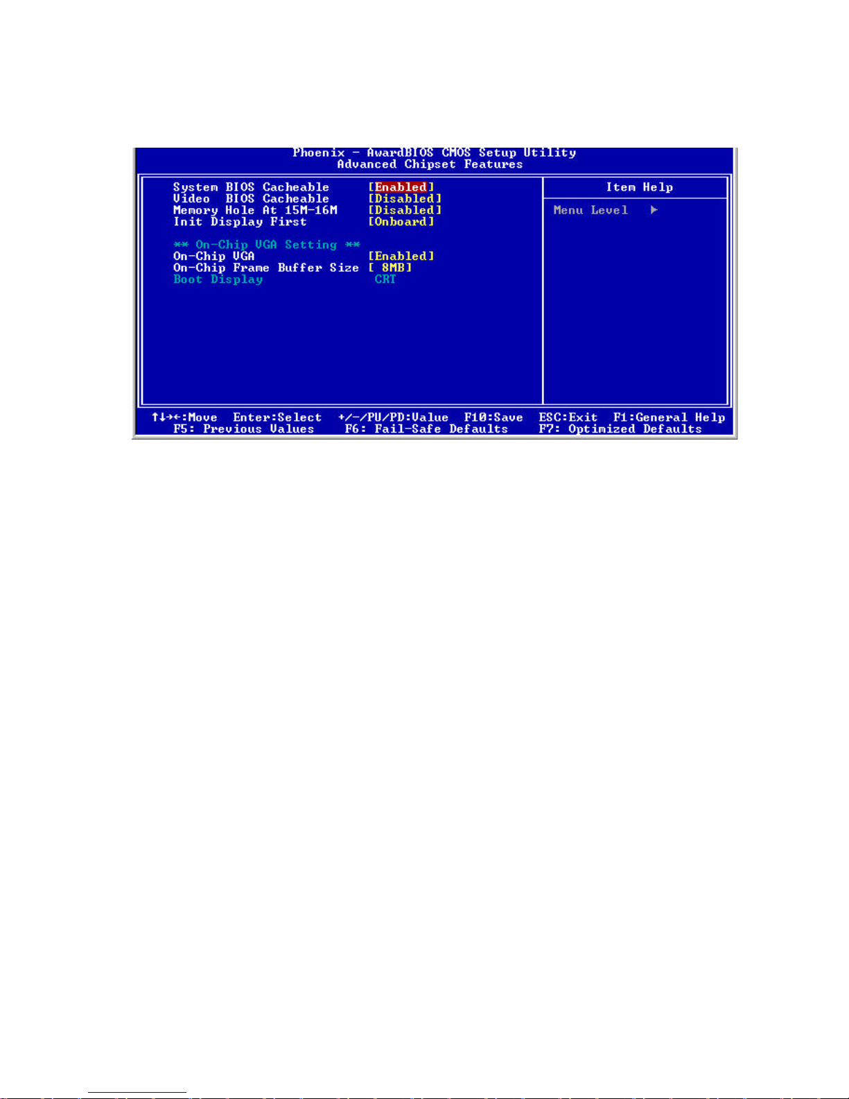
Figure 4-5 : BIOS- Advanced Chipset Features
Syste m BIOS Cacheable
Selecting Enabled allows caching of the system BIOS ROM at F0000h-FFFFFh,
resulting in better system performance. However, if any program writes to this
memory area, a system error may result. The available choices are Enabled,
Disabled.
4.7 Advanced Chipset Features
45
Video BIOS Ca cheable
Selecting Enabled allows caching of the video BIOS ROM at C0000h, resulting in
better video performance. However, if any program writes to this memory area, a
system error may result. The choices : Enabled, Disabled.
M emory Hole at 15M-16M
In order to improve performance, certain space in memory is reserved for ISA cards.
This memory must be mapped into the memory. The choices: Enabled, Disabled.
Init Display First
This item allows you to activate PCI slot or onboard display first. The choices are: PCI
slot, Onboard/AGP.
Page 47
On-chip VGA
By default, the On-Chip VGA or chipset-integrated VGA is Enabled.
On-chip Fra me Buffer Size
The On-Chip Frame Buffer Size can be set as 1MB or 8MB. This memory is shared
with the system memory.
Boot Display
Use this field to select the type of device you want to use as the display(s) of the
system.
46
4.8 Integrated Peripherals
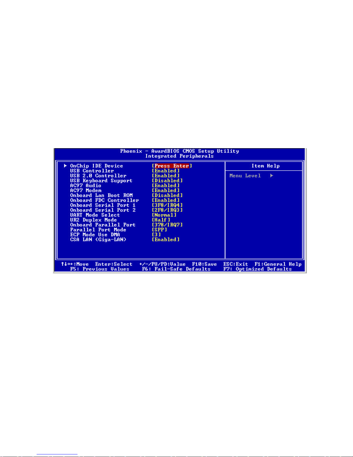
Figure 4-6 : BIOS- Integrated Peripherals
On-Chip IDE Device
The system chipset contains IDE HDD Block mode, and a PCI IDE interface with
support for two IDE Primary (Master & Slave) PIO’s and two IDE Primary (Master &
Slave) UDMA’s, and two IDE Secondary (Master & Slave) PIO’s and two IDE Second-
ary (Master & Slave) UDMA’s. Select Enabled to activate the primary and/or second-
ary IDE interface. Select Disabled to deactivate this interface, if you install a primary
and/or secondary add-in IDE interface.
On-Chip Serial ATA
This setting is used to specify the SATA controller. Settings: Disable, Auto Combined
Mode, Enhanced Mode, SATA only. If <Combined Mode> is selected, PATA and
SATA will both be enabled. If <Auto> is selected, PATA and SATA will be arranged by
Page 48

47
USB Controller
Select Enabled if your system contains a Universal Serial Bus controller and you have
USB peripherals.
U SB 2.0 Contoller
If BIOS itself has high speed USB support built in, the support will be automatically turn
on when high speed device is attached.
U SB Keyboard Support
Select Enabled if your USB controller is enabled and it needs USB keyboard support
in legacy (old) OS operating systems such as DOS.
BIOS, and you will be able to see the IDE device status listed in Standard CMOS
Features.
Serial ATA Port O/I Mode
Select a compatible mode for Port 1 and Port 2 from Award Setting to the chipset
settings:
Primary Master: Compatible Mode with Serial ATA Port 1 set to Primary Master
Primary Slave: Compatible Mode with Serial ATA Port 1 set to Primary Slave
Secondary Master: Compatible Mode with Serial ATA Port 1 set to Secondary Master
Secondary Slave: Compatible Mode with Serial ATA Port 1 set to Secondary Slave
Primary Master: Compatible Mode with only Serial ATA Enabled and Port 1 set to Primary
Master
Secondary Master: Compatible Mode with only Serial ATA Enabled and Port 1 set to
Secondary Master
SATA 1 Master: Enhance Mode with Port 1 set to Native Mode Master
SATA 2 Master: Enhance Mode with Port 2 set to Native Mode Master
Page 49

AC97 Audio
Selecting Auto will enable the AC97 audio if it is detected onboard.
AC97 M odem
Selecting Auto will enable the AC97 modem if it is detected onboard.
Onboard LAN Boot ROM
Decides whether to invoke the boot ROM of the onboard LAN chip. The available
choices are LAN1, LAN2, and Disabled.
Onboard FDC Controller
Select Enabled if your system has a floppy disk controller (FDC) installed on the sys-
tem board and you wish to use it. If you install an add-in FDC or the system has no
floppy drive, select Disabled in this field.
Onboard Serial Ports (1, 2)
Select an address and corresponding interrupt for the first and second serial ports.
The choices: Auto, 3F8/IRQ4, 3E8/IRQ4, 2F8/IRQ3, 2E8/IRQ3, Disabled.
U ART M ode Select
This item allows you to select UART mode.
The choices: Normal, IrDA, ASKIR.
U R2 Duplex M ode
In an infrared port mode, this field appears. Full-duplex mode permits simultaneous
two-direction transmission. Half-duplex mode permits transmission in one direction
only at a time. Select the value required by the IR device connected to the IR port.
Onboard Serial Ports (1, 2, 3, 4)
This feature allows you to manually select the I/O address and IRQ for the first and
second serial ports. It is recommended that you leave it as Auto so that the BIOS can
select the best settings for it. But if you need a particular I/O port or IRQ that's been
taken up by this serial port, you can manually select an alternative I/O port or IRQ for it.
You can also disable this serial port if you do not need to use it. Doing so frees up the
I/O port and IRQ used by this serial port. Those resources can then be reallocated for
other devices to use.
48
Page 50
49
Parallel Port M ode
The choices available include SPP, EPP, ECP and ECP+EPP.
ECP M ode Use DMA
When the on-board parallel port is set to ECP mode, the parallel port can use DMAS
or DMA 1. After you have made your selections in the Integrated Peripherals setup,
press the <ESC> key to go back to the main program screen.
CSA LAN (Giga-LAN)
Select Enabled for CSA LAN function.
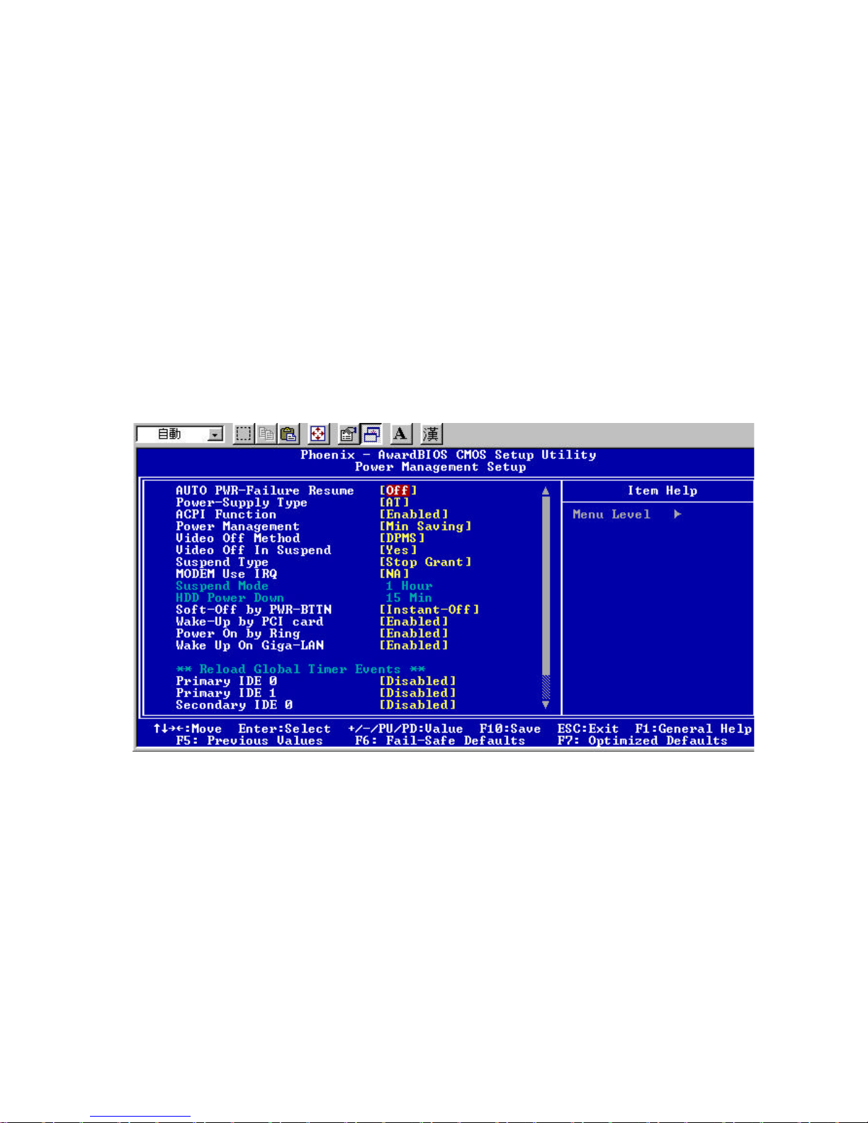
4.9 Power Management Setup
Figure 4-7 : BIOS -- Power M anagement Setup
Auto PWR -Failure Resume
This setting specifies whether your system reboots after a power failure.
There are three selections:
Off: The system will remain off when power comes back after a power failure.
On: The system will switch on when power comes back after a power failure.
Former-Sts: The system will return to the last state before the power failure when power
returns.
Page 51

Power Supply Type
The choices: AT, ATX.
ACPI Function
The ACPI standard (Advanced Configuration and Power Interface) allows the operat-
ing system to directly check the functions of energy saving and the PnP (Plug and
Play) functionality. The ACPI functions are normally activated by the BIOS. The
choices are: Enabled and Disabled.
50
Power Management
This category allows you to select the type (or degree) of power saving and is directly
related to the following modes: HDD Power Down, Doze Mode and Suspend Mode
? Min. Saving: Minimum power management
? Max Saving: Maximum power management
? User Define: Allows you to set each mode individually
Video Off Method
This determines the manner in which the monitor is blanked. There are three choices:
1. V/H SYNC+Blank: This selection will cause the system to turn off the vertical and
horizontal synchronization port and write blanks to the video buffer.
2. Blank Screen: This option only writes blanks to the video buffer.
3. DPMS Support: Select this option if your monitor supports the Display Power
Management signaling (DPMS) standard of the Video Electronics Standard to
select video power management values.
Video Off In Suspend
This determines the manner in which the monitor is blanked. The choices: Yes, No.
Suspend Type
Select the Suspend Type.
The Choices: PwrON Suspend, Stop Grant.
M ODEM Use IRQ
This determines the IRQ in which the MODEM can use.
The Choices: 3, 4, 5, 7, 9, 10, 11, NA.
Suspend Mode
When enabled and after the set time of system inactivity, all devices except the
CPU will be shut off. The choices are: 1~2 min, 2~3 min,... up to 1 hour.
H DD Power Down
When enabled and after the set time of system inactivity, the hard disk drive will be
powered down while all other devices remain active.
Page 52

Wake up by PCI Card
When the system enters a Soft-off mode (Standby power exist but system is not
working), it will wake up system when specific signals occurred. The BIOS monitors
the system for “activity” to determine when to enable power management.
If you enable this feature, the computer specifies that any signal noticed on the PCI
(Peripheral Component Interconnect) bus channel must go out from the hibernation
state. The choices: Enabled, Disabled.
Power On by Ring
An input signal on the serial Ring Indicator (RI) line (in other words, an incoming call on
the modem) awakens the system from a soft off state. The choices: Enabled,
Disabled.
Reload Global Timer Events
Primary IDE 0
Primary IDE 1
Secondary IDE 0
Secondary IDE 1
FDD, COM , LPT Port
PCI PIR Q[A-D] #
The events are I/O events whose occurrence can prevent the system from entering a
power saving mode or can awaken the system from such a mode. In effect, the sys-
tem remains alert for anything which occurs to a device which is configured as
Enabled, even when the system is in a power down mode. The choices: Enabled,
Disabled.
51
Soft-Off by PWR BTN (Power Button)
Pressing the power button for more than 4 seconds forces the system to enter the
Soft-Off state when the system “hangs”. The available choices are Delay 4 Seconds,
Instant-Off
Page 53
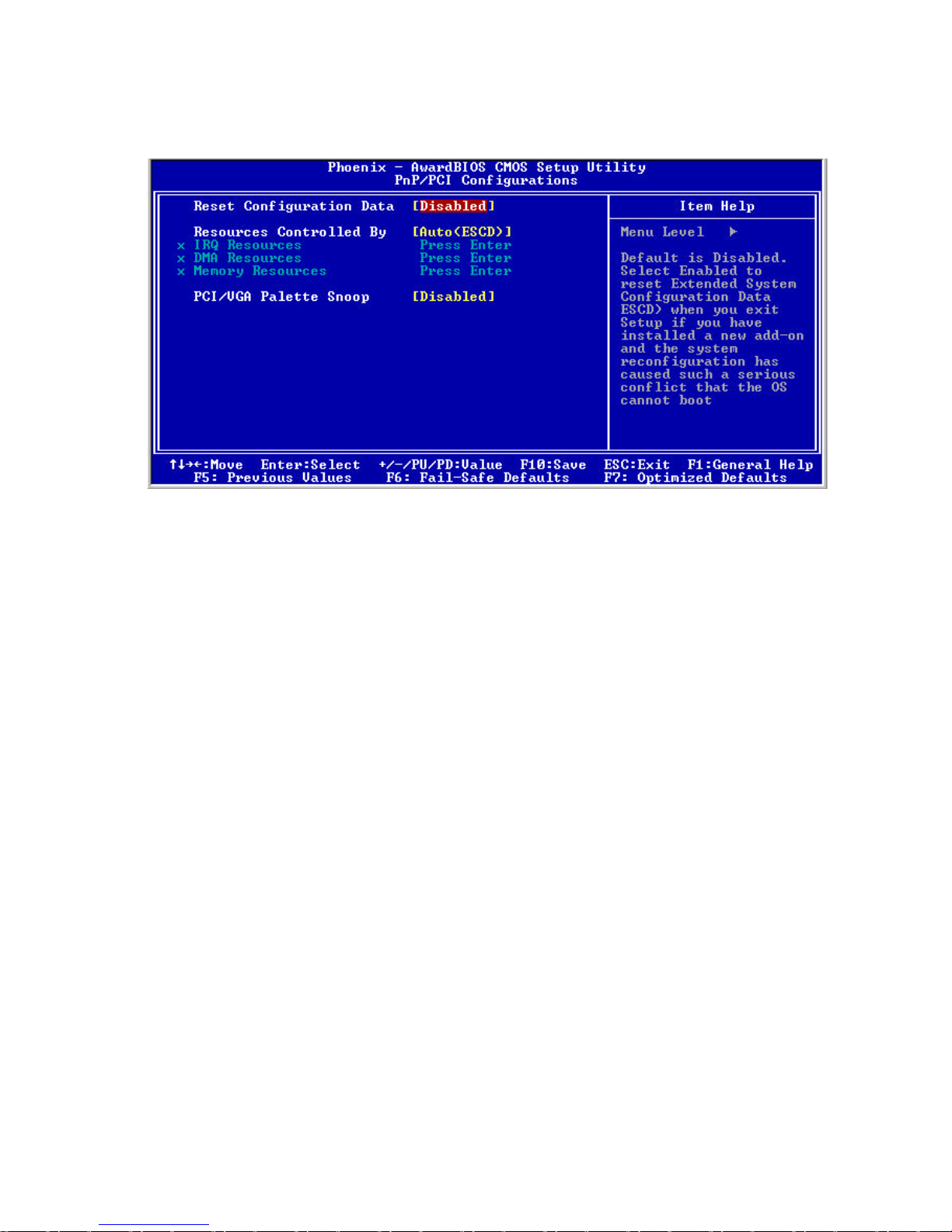
4.10 PnP/PCI Configurations
R eset Configuration Data
Normally, you leave this field Disabled. Select Enabled to reset Extended System
Configuration Data (ESCD) when you exit Setup if you have installed a new add-on
Card and the system reconfiguration has caused such a serious conflict that the
operating system cannot boot.
The choices: Enabled, Disabled .
R esources Controlled By
The Award Plug and Play BIOS has the capacity to automatically configure all of
the boot and Plug and Play compatible devices. However, this capability means
absolutely nothing unless you are using a Plug and Play operating system such as
Windows95. If you set this field to Manual, then choose specific resources by
going into each of the submenus that follows this field.
The Choice: Auto (ESCD), Manual.
PCI/VGA Palette Snoop
Leave this field at Disabled. The Choices: Enabled, Disabled.
Figure 4-8 : BIOS -- PnP/PCI Configurations
52
Page 54
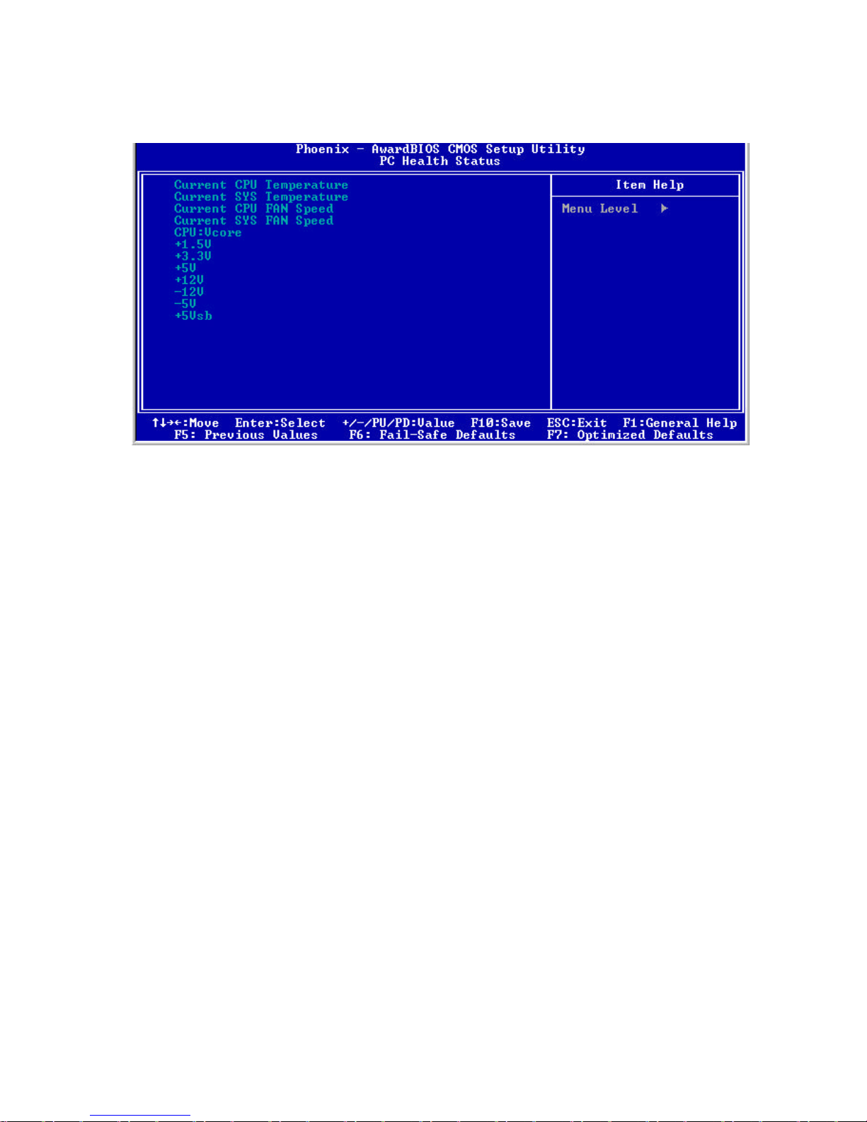
4.11 PC Health Status
Figure 4-9 : BIOS- PC Health Status
53
After you have read the PC Health Status, press the <ESC> key to go back to the main
program screen.
Page 55

4.11 Load Fail-Safe Defaults
This option opens a dialog box that lets you install fail-safe defaults for all appropri-
ate items in the whole setup utility.
Use this option if you have changed your system and it does not operate correctly
or does not power up.
4.12 Load Optimized Defaults
This option opens a dialog box that lets you install optimized defaults for all appropri-
ate items in the whole Setup Utility. Press the <Y> key and then <Enter> to install the
defaults. Press the <N> key and then <Enter> to not install the defaults. The optimized
defaults place demands on the system that may be greater than the performance level
of the components, such as the CPU and the memory. You can cause fatal errors or
instability if you install the optimized defaults when your hardware does not support
them. If you only want to install setup defaults for a specific option, select and display
that option, and then press the <F7> key.
4.13 Set Supervisor/User Password
The Supervisor/User Password utility sets the password. The mainboard is shipped
with the password disabled. If you want to change the password, you must first
enter the current password, then at the prompt enter your new password. The
password is case sensitive. You can use up to eight alphanumeric characters.
Press <Enter> after entering the password. At the next prompt, confirm the new
password by retyping it and pressing <Enter> again.
To disable the password, press <Enter> instead of entering a new password when
the Enter Password dialog box appears. A message appears confirming that the
password has been disabled.
If you have set supervisor and user passwords, only the supervisor password
allows you to enter the BIOS Setup Program.
Note: If you forge t your password, the only way to solve this problem is to
discharge the CMOS m emory by turning power off and placing a shunt (jumper
cap) on jum per JP2 to short pin 2 and pin 3 for five seconds, then putting the
shunt back to pin 1 and pin 2 of JP2.
54
Page 56

4.14 Save & Exit Setup
Selecting this option and pressing <Enter> will save the new setting information in the
CMOS memory and continue with the booting process.
4.15 Exit Without Saving
Selecting this option and pressing <Enter> will exit the Setup Utility without recording
any new values or changing old ones.
55
Page 57

56
Chapter 5
Driver Installation
Page 58
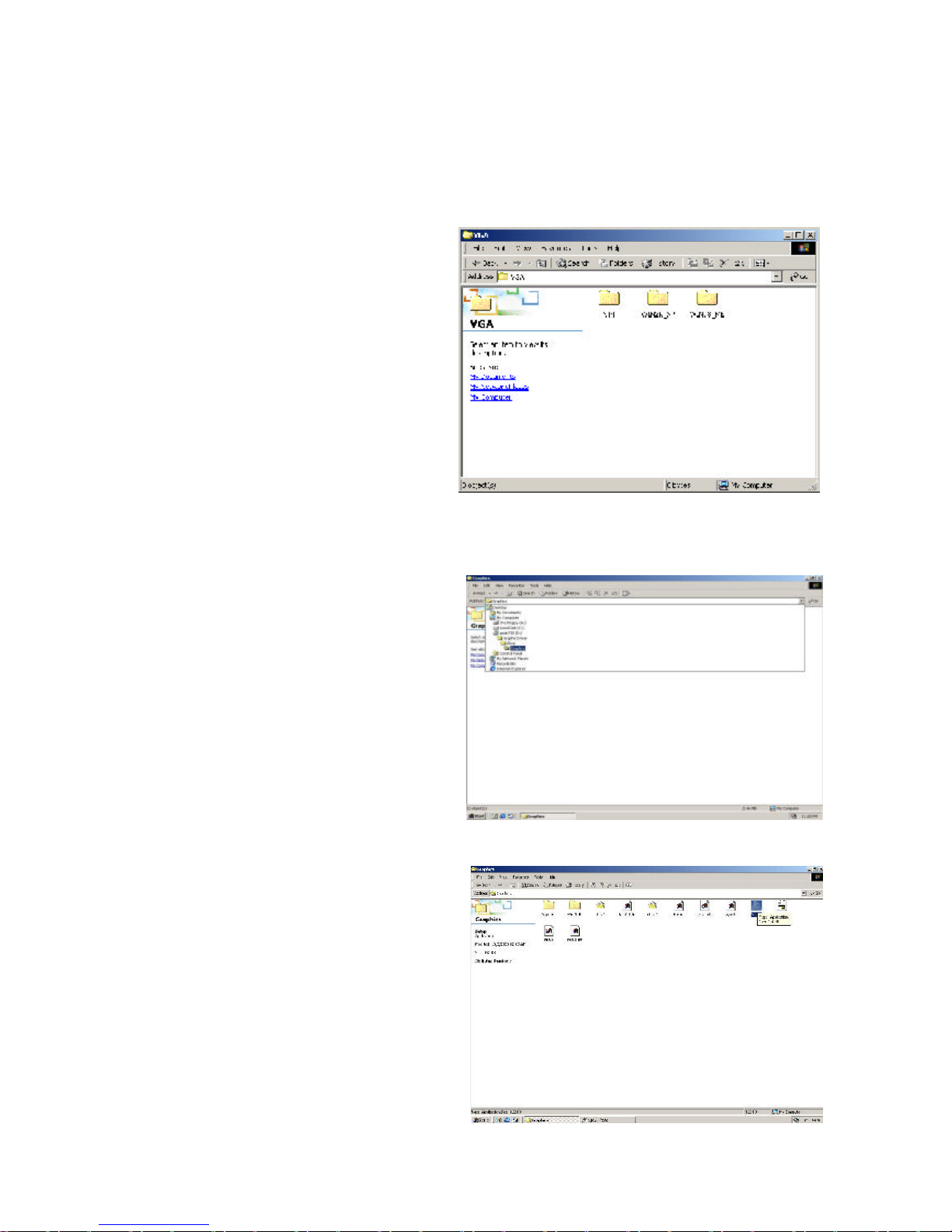
5.1 Installing VGA Driver
Ste p 5.1.1
Double click the folder of VGA.
The menu will display.
Select the folder of WIN 2K_XP
for Windows 2000 operating system.
Ste p 5.1.2
After the menu displays, select the
folder of GR APHICS.
57
PEAK 735 Series comes with a driver installation CD-ROM that enables you to install
VGA driver software, INF(Intel Chipset Software Installation Utility), LAN and USB.
Ste p 5.1.3
After this screen displays,
double click the blue sign
SETU P.
Page 59
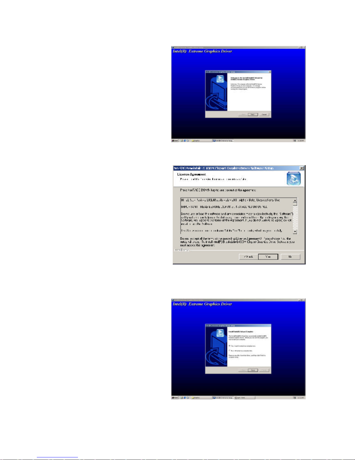
Ste p 5.1.4
After a sequence of system
processing, you will see a
static screen instructing the
installation process.
Click N ext to continue setup.
Ste p 5.1.5
If you accept License Agreement,
click Ye s to continue.
58
Ste p 5.1.6
An installation wizard will inform
successful completion of driver
software installation and ask you
to restart your computer.
Select “Ye s, I want to restart my
computer now,” and then click
Finish.
After your computer reboots,
VGA driver is already setup in
your computer.
Page 60
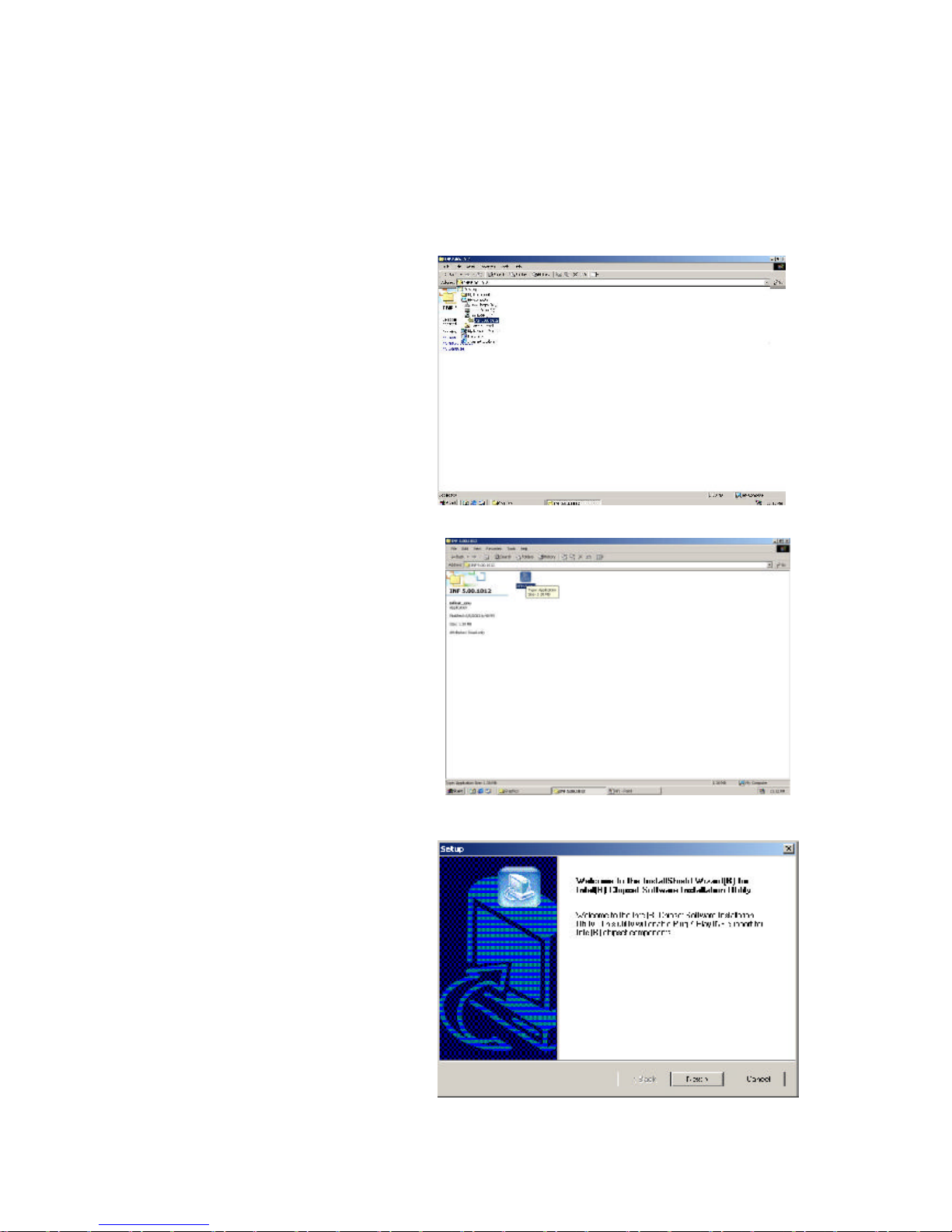
5.2 Installing INF
After installing VGA driver, go back to 5.1. Go through step 5.11 to step 5.14
again, and open the folder of INF to start installing INF.
Ste p 5.2.1
Open the folder of
IN F 5.00.1012
Ste p 5.2.2
Double click the blue sign
IN FINST_ENU
Ste p 5.2.3
Click N ext to install INF.
59
Page 61
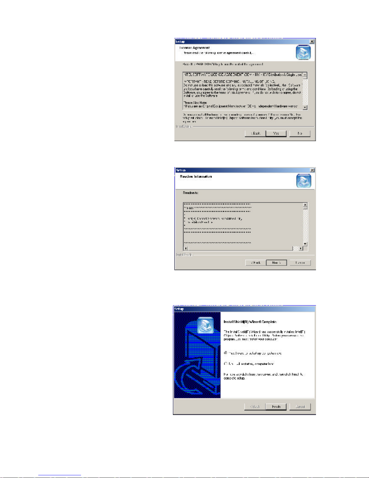
Ste p 5.2.4
Click Yes to continue.
Ste p 5.2.5
Click Yes.
Ste p 5.2.6
Select Ye s, I want to restart
my computer now.
Then click Finish.
INF is installed.
60
Page 62
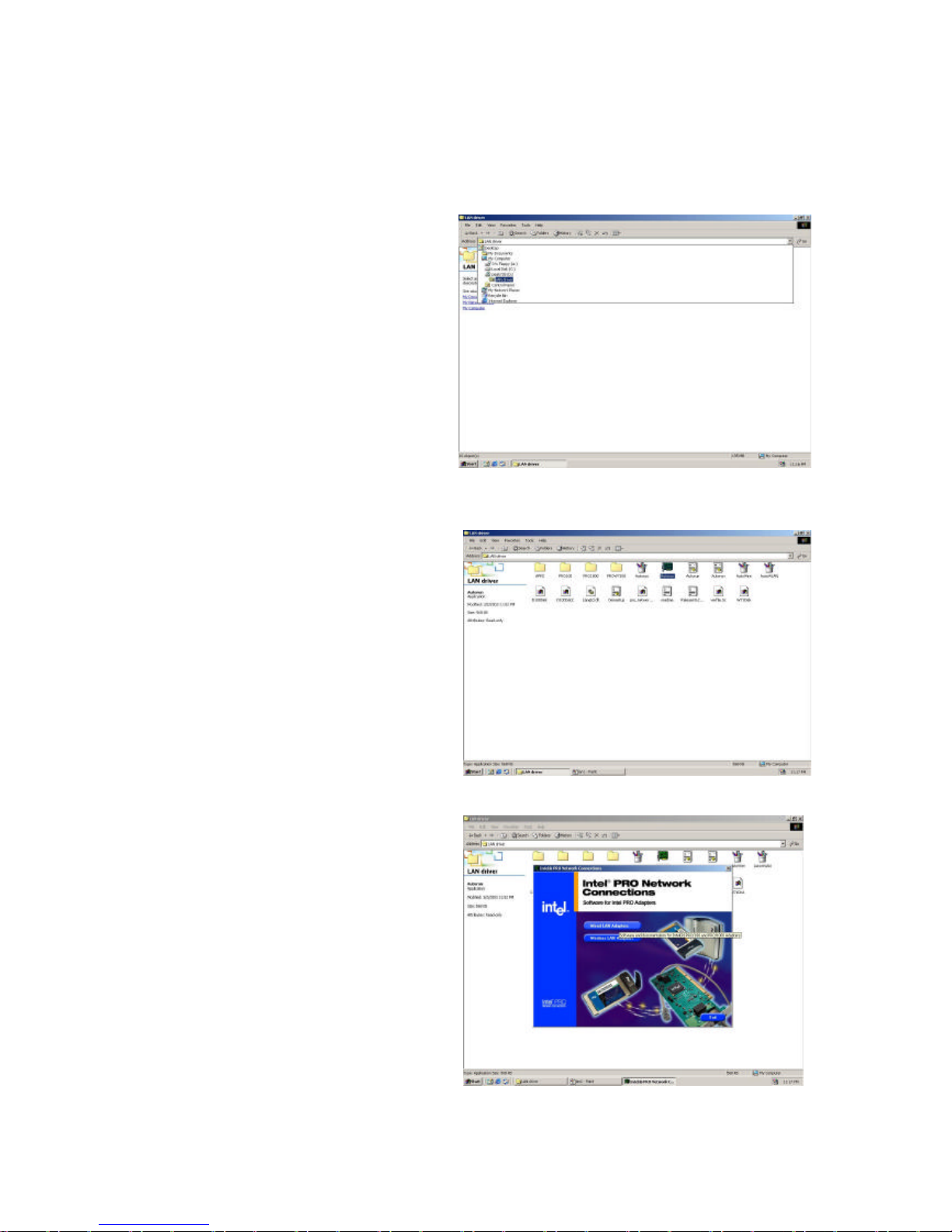
5.3 Installing LAN
After installing INF, go back to 5.1. Go through step 5.1.1 to step 5.1.4 again, and
open the folder of LAN driver.
Ste p 5.3.1
After the folder of LAN driver
displays, click it.
Ste p 5.3.2
Double click the Autorun Icon
Ste p 5.3.3
Click Wired LAN Ada pter or
Wirele ss LAN Adapter for
installation
61
Page 63
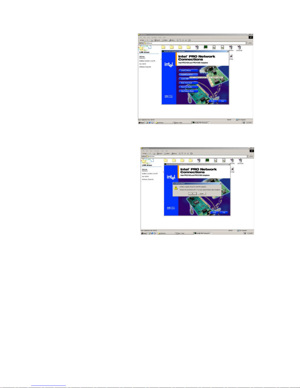
Ste p 5.3.4
Install or update the minimum
drivers for Intel PR O ada pters.
62
Ste p 5.3.5
Install or update drivers
for Intel PRO adapters.
Page 64
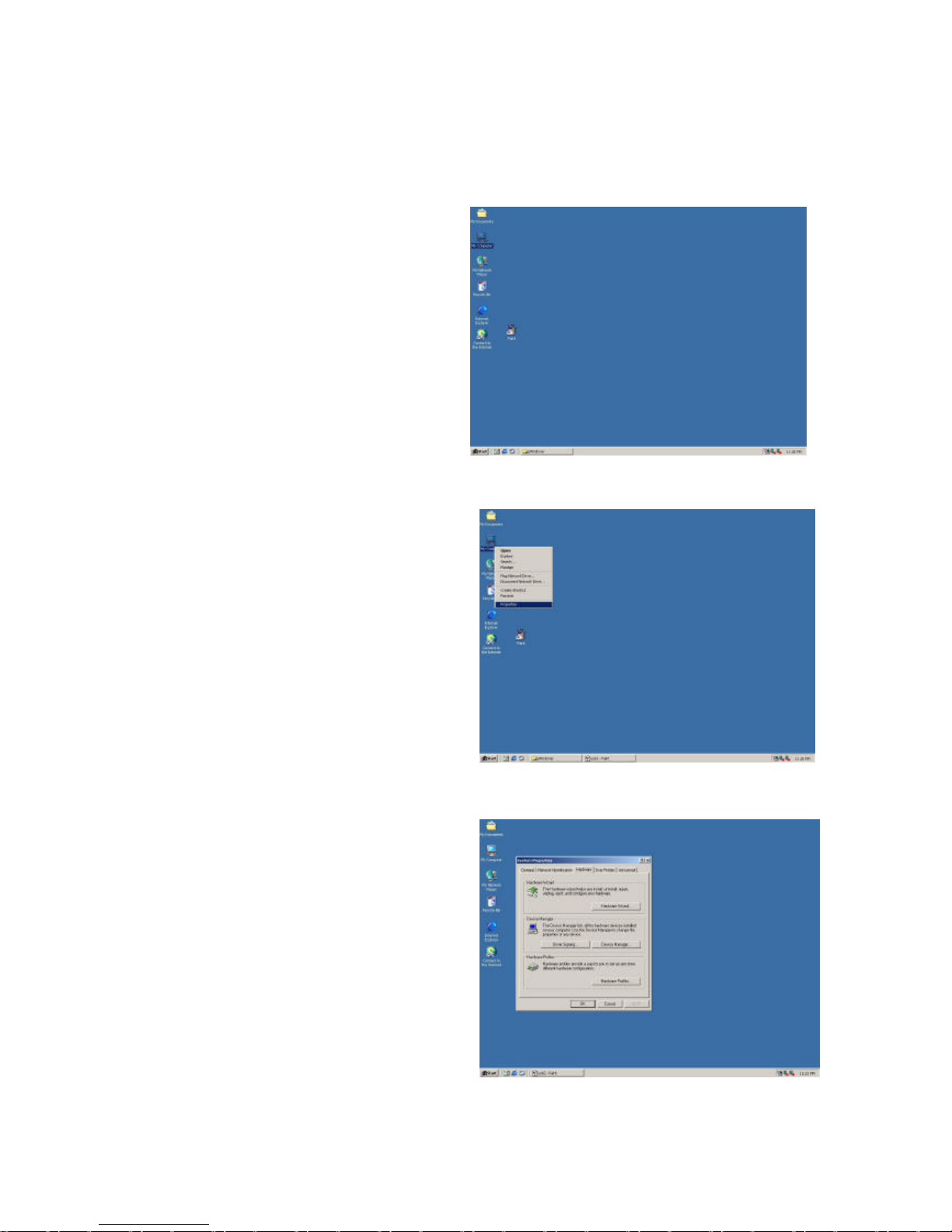
5.4 Installing USB
After installing the LAN driver, go back to computer desktop and open My Computer.
Step 5.4.1
Double click the My Computer
icon to open it.
Step 5.4.2
Choose Properties in the drop menu.
Step 5.4.3
Click OK in the System Properties
Menu.
63
Page 65
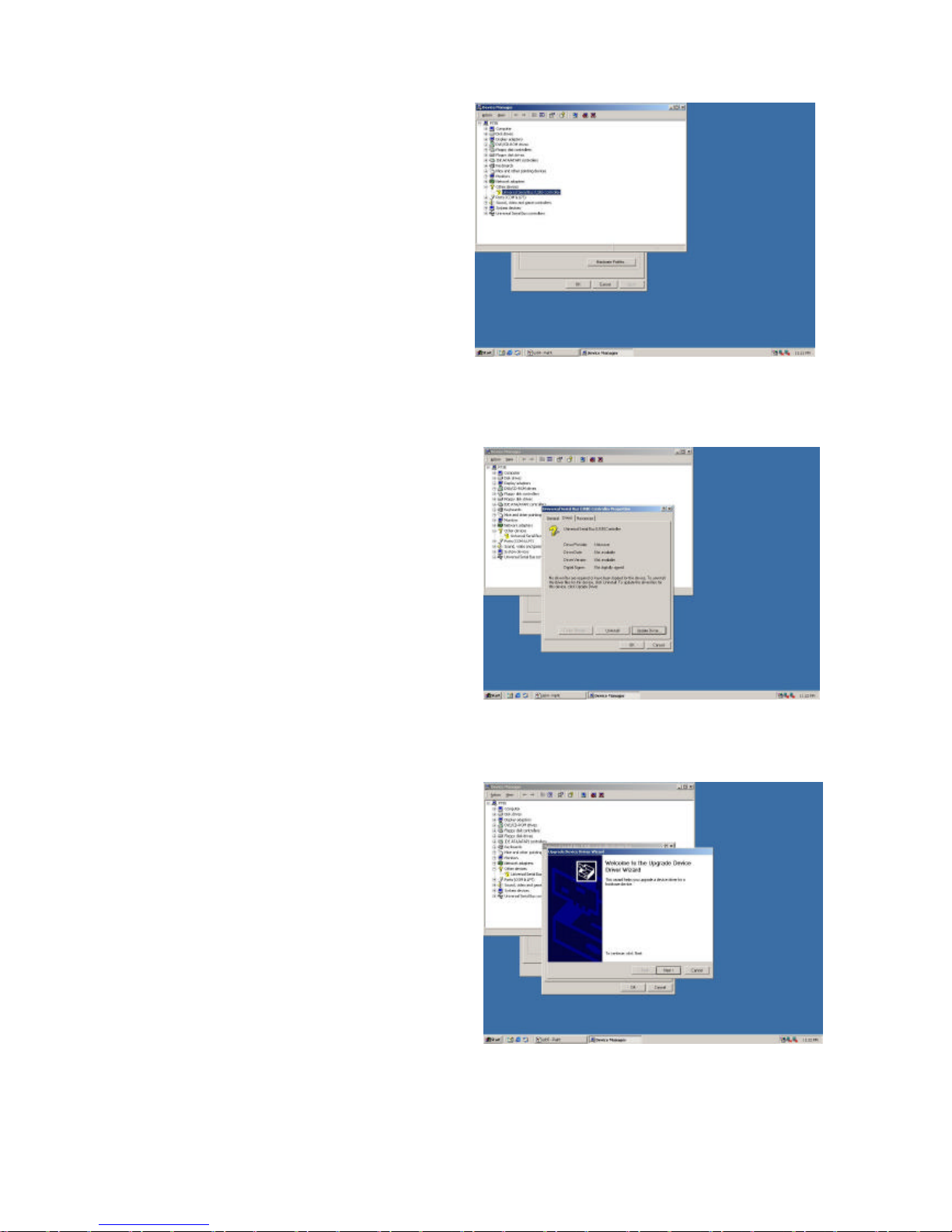
Step 5.4.4
Click USB Controller in the
Device Manager folder.
Step 5.4.5
To update the driver files for
this device, click Update Driver.
Step 5.4.5
To continue, click Next.
64
Page 66
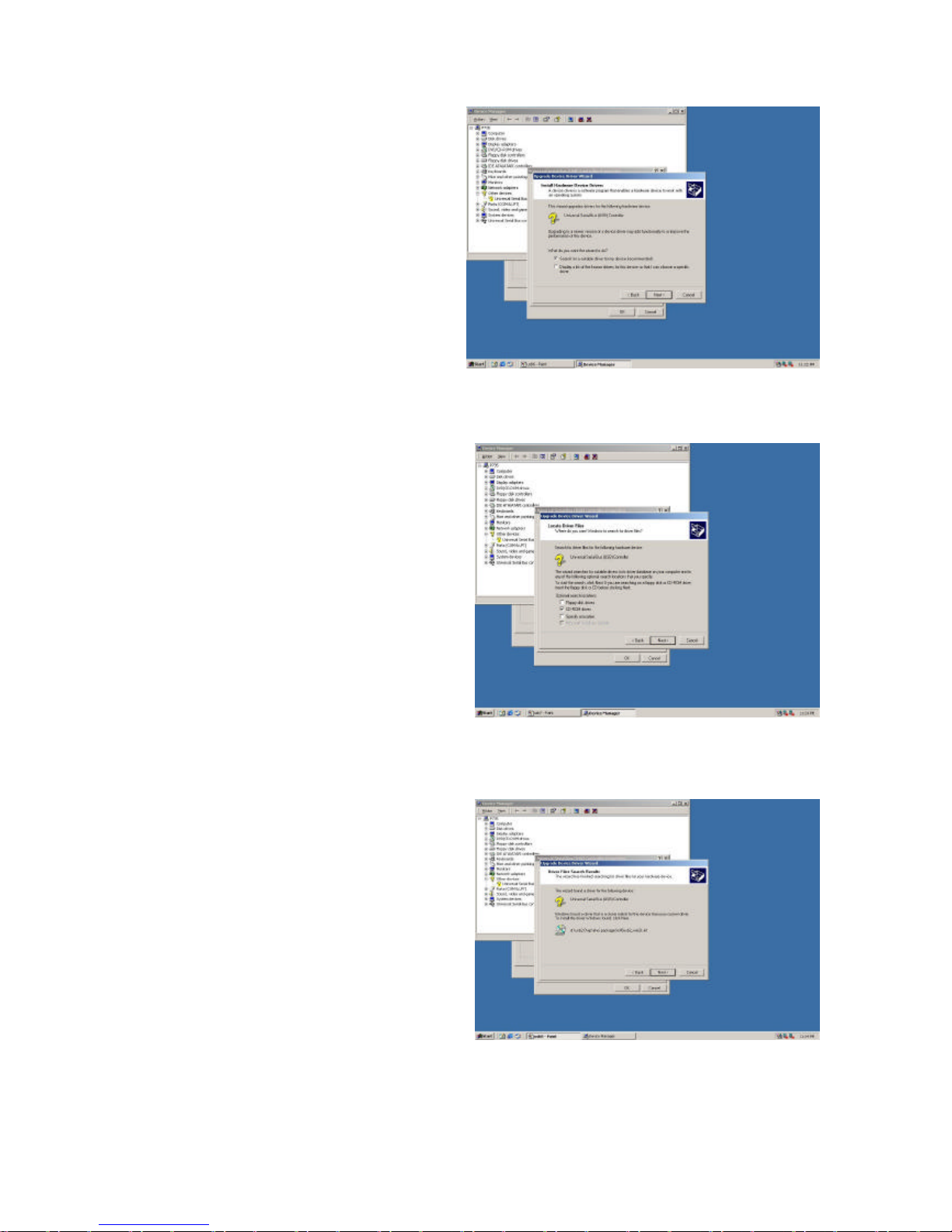
Step 5.4.5
To upgrade a device driver, click Next.
Step 5.4.6
To upgrade a device driver, click Next.
Step 5.4.7
To install the driver Windows found,
click Next.
65
Page 67
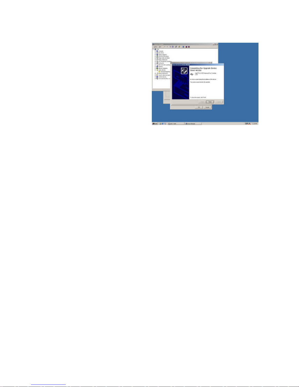
Step 5.4.8
To close this wizard, click Finish.
66
Page 68

Appendix A : Watchdog T imer Setting
A.1 Watchdog Timer Working Procedure
Watchdog Timer (WDT) is a special hardware device that monitors the computer
system during normal operation. WDT has a clock circuit that times down from a
set number to zero. If a monitored item occurs before the timer reaches zero, WDT
resets and counts down again. If for some reason the monitored item doesn’t
occur before the timer reaches zero, WDT performs an action, such as a diagnos-
tic operation (rebooting the computer).
You must enter timer values into WDT Configuration Register (Write the control
value to the Configuration Port), and clear WDT counter (read the Configuration
Port).
WDT Configurat ion port F2 Default at F2
Wat ch Dog Timer Disabled 1. Default at disabled
Enabled 2. Enabled for user’s programming
WDT Act ive Time 1 sec Default at 64 sec
2 sec
4 sec
8 sec
16 sec
32 sec
64 sec
128 sec
Table A-1 : Watchdog Timer Character and Function
67
Page 69
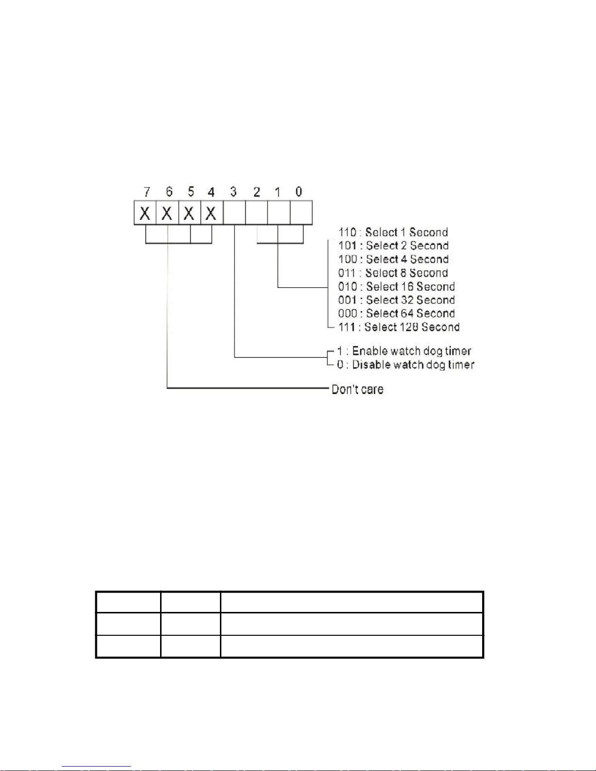
A.2 Watchdog Timer Control Register
The Watchdog Timer Control Register controls the WDT working mode. Write the
value to the WDT Configuration Port. The following table describes the Control
Register bit definition:
A.3 Watchdog Timer Programming Procedure
·
A.3.1 Power On or R eset the Syste m
The initial value of WDT Control Register (D3~D0) is zero (0), when power is on or
the system has been reset. The following table indicates the initial value of WDT (
00000000b ) :
Bit Value Mean
3 0 Disable Watchdog Timer
2, 1, 0 0 0 0 Select 64 second
Table A-3 : WDT Control Register Initial Value
Table B-2 : WDT Control R egister Bit Definition
68
Page 70

WDT counter interval cannot be longer than the preset time, otherwise, WDT
sends a reset signal to the system.
The following is an example of clearing the WDT program in Intel 8086 assembly
language.
; ( Clear the WDT)
Mov dx, F2h ;Setting the WDT configuration port
In al, dx
N ote: Before running WDT, you must clear WDT to ensure
that the initial value is zero.
A.3.3 WDT Control R egister
N ote: This register writes to WDT configuration port.
Set WDT Control Register to control the WDT working mode. The initial value of
WDT Control Register is shown as follows:
; (Setting the WDT Control Register as AL)
Mov al, 0h ; Setting initial value = 0 for the WDT Control Register
Follow these instructions to set the register:
1. Select the time-out intervals of WDT (decide the values of D2, D1, D0 in F2 )
Example: If D2~D0 = 0, the time-out interval is 64 seconds.
AND al, 11111000b ; Setting the time-out interval as 64 sec.
2. Enable or Disable WDT ( decide D3 value in F2)
i.e. D3=0, Disables WDT
A.3.2 Cle ar the WDT
AND al, 11110111b ; Disable the WDT
69
Page 71
i.e. D3=1, Enables WDT
OR al, 00001000b ; Enable the WDT
After finishing the above settings, you must output the Control Register’s value to
WDT Configuration Port. Then WDT will start according to the above settings.
MOV dx, F2h ; Setting WDT Configuration Port
OUT dx, al ; Output the Control Register Value
70
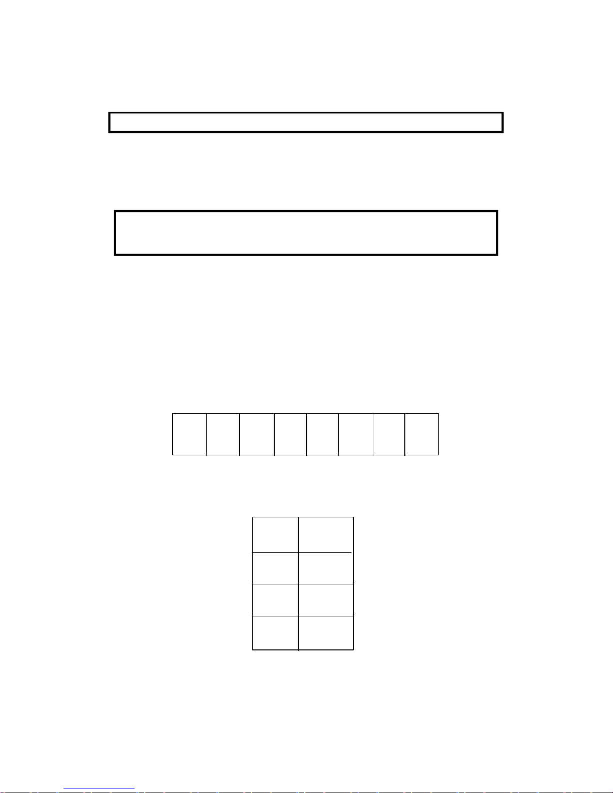
Appendix B:GPIO USER GUIDE
DIGITAL I/O UESD PORT 801
JP17
IN 0
IN 1
IN 2
IN 3
OUT 0
OUT 1
OUT 2
OUT 3
1 2
3 4
5 6
7 8
I3 I2 I1 I0 O3 O2 O1 O0
{ } { }
Input Output
 Loading...