

Page 1

2/26/20022:06 PM
NMIY-0031
Single Board
1
Computer
Covers: NMIY-0031 V1.0 4/22/96
Page 2

2/26/20022:06 PM
2
Page 3

2/26/20022:06 PM
NMIY-0031 TABLE OF CONTENTS
3
Table of Contents
TABLE OF CONTENTS ..............................................................................................................................3
PART I ...........................................................................................................................................................5
INTRODUCTION .........................................................................................................................................5
ONVENTIONS
C
ETTING STARTED
G
...............................................................................................................................................7
........................................................................................................................................9
BASIC USERS.........................................................................................................................................10
MONITOR USERS ..................................................................................................................................10
FORTH USERS.......................................................................................................................................11
PART II ........................................................................................................................................................13
HARDWARE...............................................................................................................................................13
IRCUIT DESCRIPTION
C
................................................................................................................................15
POWER...................................................................................................................................................16
PROCESSOR ..........................................................................................................................................16
BOARD CONFIGURATION...................................................................................................................16
MEMORY SOCKETS ..............................................................................................................................17
I/O INTERFACES ...................................................................................................................................17
PROTOTYPING AREA ...........................................................................................................................18
I/ O C
ONNECTORS
.......................................................................................................................................19
POWER - J12..........................................................................................................................................19
KEYPAD - J3 ..........................................................................................................................................19
LCD - J6..................................................................................................................................................20
RS232 - J10.............................................................................................................................................20
OPTIONAL CONNECTORS ...................................................................................................................21
RS422/485 - J11......................................................................................................................................21
VERTICAL STACKING CONNECTORS - J1, J7, J9..............................................................................21
LATCHED and NON-LATCHED I/O - J4 and J5 ..................................................................................22
UMPERS
J
.....................................................................................................................................................23
MEMORY CONFIGURATION JUMPERS .............................................................................................23
RESET.....................................................................................................................................................24
LCD CONTRAST ....................................................................................................................................25
VERTICAL STACKING COMPONENT (VSC) CONFIGURATION JUMPERS....................................25
SERIAL COMMUNICATIONS CONFIGURATION JUMPERS.............................................................26
ROUBLESHOOTING
T
....................................................................................................................................27
MOUNTING............................................................................................................................................27
POWER SUPPLY....................................................................................................................................27
OPERATING SYSTEM............................................................................................................................27
MEMORY................................................................................................................................................28
TERMINAL .............................................................................................................................................28
KEYPAD and LCD I/O ...........................................................................................................................28
PHYSICAL INSTALLATION OF DEVICES ...........................................................................................28
OARD MOUNTING
B
.....................................................................................................................................29
NMIY-0031 MOUNTING........................................................................................................................29
VSC MOUNTING....................................................................................................................................29
Page 4

2/26/20022:06 PM
4
PART III ......................................................................................................................................................31
SOFTWARE ................................................................................................................................................31
ROGRAMMING
P
...........................................................................................................................................33
MEMORY................................................................................................................................................33
DATA PORTS..........................................................................................................................................35
KEYPAD I/F............................................................................................................................................35
LCD I/F...................................................................................................................................................36
SERIAL I/O .............................................................................................................................................38
ROGRAM SEGMENTS
P
..................................................................................................................................39
MONITOR...............................................................................................................................................39
BASIC......................................................................................................................................................41
C..............................................................................................................................................................43
FORTH....................................................................................................................................................46
PART IV.......................................................................................................................................................49
DRAWINGS ................................................................................................................................................49
ARTS LIST
P
ILK SCREEN
S
ECHANICAL DRAWING
M
CHEMATIC
S
.................................................................................................................................................51
...............................................................................................................................................53
.............................................................................................................................55
.................................................................................................................................................57
....................................................................................................................................................................57
APPENDICES .............................................................................................................................................59
APPENDIX A ..............................................................................................................................................61
APPENDIX B.............................................................................................................................................101
APPENDIX C ............................................................................................................................................147
Page 5

2/26/20022:06 PM
NMIY-0031 PART I INTRODUCTION
5
PART I
Introduction
The NMIY-0031 board is a low cost, production oriented, computer board. Facilities are
included for serial communications, LCD interface, keypad, memory expansion to 64Kbytes of
data and memory each, and raw and latched parallel I/O. It can serve as host for the NMIL
series of Vertical Stacking Component (VSC) cards. This ability gives it a great degree of
flexibility in meeting customer application requirements. The NMIY-0031 design allows
purchasers to configure the board, including only the hardware facilities required by their
application.
The NMIY-0031 has several options that make it adaptable to many uses. The standard
configuration is used as a base to allow the user many paths to achieving the control configuration
that suits their application. To provide the facilities that promote application development, the
installed headers option allow flexibility in configuring memory. Three languages for
development, as well as a monitor, are also available. Other options include an on board power
supply, up to a 64K program EPROM, up to two 32K data ram chips, and three COM port
standards. Customized circuitry can be added in the prototyping area.
Vertical Stacking Component (VSC) options further enhance flexibility. More than a dozen
NMIL series peripheral cards are available to enhance off the shelf hardware solutions for control
systems. Custom card designs can also make use of the VSC connector for connection.
With the combination of 64K program space, 64K data space, and fully customizable interfaces,
the NMIY-0031 processor board provides the user with the ability to construct a cost-effective,
digital control unit for a wide range of applications.
Conventions describes the use of print conventions in this manual.
Getting Started
provides some basic functional checks so that the user may quickly determine
the status of the hardware.
Page 6

2/26/20022:06 PM
6
Page 7

2/26/20022:06 PM
NMIY-0031 CONVENTIONS
7
Conventions
Several different type faces are used in this manual to distinguish items such as user input, screen
output, etc. This is a guide to reading the type-face conventions employed.
Conventions
typeface is used to distinguish chapter titles at the beginning of each
section.
FORTH indicates the formal name of a language, or a title reference to another manual chapter or
chapter subsection title.
Enter highlighting signifies a key name for function keys. In a program dialog, highlighting
indicates a user keyed data entry.
indicates a response from software or operating system.
OK
Bold text is used occasionally, where text requires special emphasis.
Command codes and addresses are always given in hexadecimal format.
Page 8

2/26/20022:06 PM
8
Page 9

2/26/20022:06 PM
NMIY-0031 GETTING STARTED
9
Getting Started
System operation requires power and communications connections. A standard configuration
board requires 250 mA of regulated +5 VDC at connector J12. The on-board power supply
option requires 6.3 to 10.0 VAC input at connector J2. The MAX232 chip develops its own +/10 VDC for RS-232C compatibility.
For development systems, a terminal (or PC with terminal emulation software) must be
connected. A cable with an RS-232 connector (DB25 or DB9) on one end and a 10-pin dual-row
header connector on the other end is required. This cable is not included with the NMIY-0031,
and must be provided by the user or purchased separately from the supplier. The RS-232 serial
connections are present at J10. Pin J10-3 is data-out and pin J10-5 is data-in to the 0031 board.
See the section on I/O Connectors for additional detail on J10 connections.
Once power and terminal connections are established, the operating system or monitor EPROM
in U2 can be used to work with basic board functions, such as the LCD or keypad interfaces.
The RS232 terminal connection requires a 9600 baud terminal with no parity, 8 data bits, and one
stop bit (8N1). On a PC, also check that the terminal emulator program is set to use the same
physical port to which you have attached the serial interface cable( i.e. COM1:, COM2:, etc.).
Examples follow for users of BASIC, Monitor, and FORTH. The examples are intended as quick
checks of board function. When the cursor (underscore) is present in an example, it will blink.
FORTH does not use a cursor.
Page 10

2/26/20022:06 PM
NMIY-0031 GETTING STARTED
10
BASIC USERS
The BASIC EPROM should be installed in U2. BASIC also requires a 32K RAM chip be
installed in U4. EEPROM may be used in U3 at the user’s option. At power on, the terminal
(or emulator) will display:
*MCS-51 ™ BASIC V1.1*
READY
>_
Å Board power on message at the terminal
Å Prompt (‘>’) followed by cursor ( ‘_’)
To verify operation, enter the command:
>PRINT “HELLO!”
HELLO!
>_
Å BASIC response; Note: no prompt on this line
Å User input
If you see something significantly different, please consult the section on Troubleshooting. For
additional information on BASIC please consult the MCS BASIC manual.
MONITOR USERS
For users with the Monitor EPROM in U2, power-on causes the system to start up and display
the message:
NMI 8051 MONITOR V1.10
TYPE ‘H’ FOR HELP
>_
Please note that the monitor commands
user put the keyboard in
CAPS LOCK
mode when using the monitor. When the user enters H (no
be upper case. We strongly recommend that the
must
enter needed), the following help menu appears on the terminal:
H
------------------------------------------------------------------------------------------------------------H :help
R <addr> :read internal data memory
D <addr> :read external data memory
P <addr> :read program memory
S <addr> :read special function register
A <addr> <size> :dump internal data memory
U <addr> <size> :dump external data memory
M <addr> <size> :dump program memory
W <addr> <size> :write onto internal data memory
O <addr> <size> :write onto external data memory
T <addr> <size> :write onto special function register
F <addr> <size> <value> :fill external data memory with value
X <addr> :execute
Z <addr> <size> :erase internal data memory
E <addr> <size> :erase external data memory
L :load INTEL HEX file
I <addr> <size> :dump memory in INTEL HEX format
------------------------------------------------------------------------------------------------------------>_
Page 11

2/26/20022:06 PM
NMIY-0031 GETTING STARTED
11
Under monitor control, the computer’s response appears on the terminal screen as soon as the
complete command is entered. When using this monitor, an enter on the terminal keyboard is
required to begin command execution. Execution begins as soon as all command characters
NOT
are fully entered at the keyboard. An enter before giving a valid command with its required data,
the monitor will issue an appropriate error message followed by a prompt. Whenever the
Monitor displays the prompt, it is ready for the next user command. The Monitor does not
recognize the backspace key.
Data format and position are crucial to success when using a monitor. Fields in angle brackets are
required and expect an exact number of characters. Numeric values such as addr, size, and value
are entered in hexadecimal (‘hex’). Example: <addr> expects a four digit hex value, <size>
expects a two digit hex value. Note that the hex digits greater than 9 require upper case. It is
recommended that the terminal be set to
CAPS LOCK
whenever hex values are to be entered.
FORTH USERS
At power on, EPROM based FORTH users will see:
Max-FORTH V1.0
This message should appear any time the card is reset including power on. The card should be
connected through J10 to a terminal or emulator at 9600 baud, 8-N-1. With the prototype area of
the board to your left, looking at the component side of the card, J10 is in the upper right hand
corner of the board. Also, J10-Pin1 will be toward the right edge of the card, away from the
processor, U1, and the prototype area.
A quick check that FORTH is operating is to enter the command WORDS. Note that this entry
will be in all caps. The screen will display a list of words (commands) and addresses provided by
the system. Expect the list to scroll off the screen:
WORDS
1E4E TASK 134F ( 1EAE Z 1EE2 IC!
1EE4 IC@ 589 @ 57C C@ 561 !
572 C! 151 2@ 140 2! F4E :
F64 ; 550 + 53E - 1B2F 1-!
1B25 1+! 1A9 +! 1E46 * 1E3C /
49E >< 4A8 SWA_ 1ACD 2OV__ 1AD9 2SW__
4FF DUP 1AC5 2DU_ 490 OVE_ 476 ROT
1AB7 2RO_ 196 PIC_ 16F ROL_ 1AF3 -R__
4E5 DRO_ 136 2DR__ 4CB >R 4D8 R>
1B39 = 390 NOT 385 0= 1EA6 D0=
375 0> 36A 0< 358 U< 332 <
DF DU< AA D< 1E9E D= 1B49 >
52D AND 50B OR 51C XOR 161C IF
1610 THE_ 15FA ELS_ 15F0 BEG__ 15E2 UNT__
15D0 REP___ 15C8 WHI__ 15BA AGA__ 15E2 END
1552 DO 1576 LOO_ 1566 +LO__ 229 K
220 J 1F9 I 1E5 R@ 1586 LEA__
630 EXI_ 790 KEY 789 EMI_ 770 ?T________
1B41 S->_ 322 ABS 1E8A DAB_ 318 MIN
1E78 DMI_ 308 MAX 1E66 DMAX 1D4A SPA___
1AE5 DEP__ 1CC5 CR 1CA5 TYP_ 1C99 COU__
1C71 -TR_______ 3BC 1+ 3D8 2+ 3C9 1-
Page 12

2/26/20022:06 PM
NMIY-0031 GETTING STARTED
3E1 2- 3AB 2/ 39D 2* 103 D+
1AA5 D- 59B D2/ 1DF8 /MO_ 1DF0 MOD
1DE4 */M__ 1DDA */ 2BA UM* 27F UM/___
23A NEG_ __ 122 DNEG __ F8C CON______ F7C VAR______
F9A 2C________ F72 2V________ 232 EXE____ 4C3 RP@
4BA SP@ 1D9A CMO ___ 6F0 CMO__ 630 ;S
FC4 COD_ FB4 END-C___ FA6 USE_ 1B7B .
1B8D .R 1B99 D. 1B73 U. 1B83 U.R
1BA3 D.R 1BFA #S 1C08 # 1BE9 SIG_
1BD9 #> 1BCF <# 1B6B ? 1CD3 EXP___
E92 QUE__ 1C2B BL 1A8C STA__ 1A89 CUR____
1A86 CONT___ 1A83 SCR 1A80 BLK 1A41 DP
1A62 OFF___ 1A77 FLD 1A74 DPL 1A6B >IN
1A35 BAS_ 1A26 SO 1A29 TIB 1A71 #T
1A6E SPA_ 1A9D C/L 1836 FIR__ 182E LIM__
1A95 PAD 1650 HER_ 1648 ALL__ 163C ,
1630 C, 1D62 SPA__ 4ED ?D__ 14F2 TRA_____
1628 LAT___ 13D0 COM____ 13C8 [ 13BE ]
1A0C HEX 1A03 DEC____ 13A6 ;CO__ 139E <BU____
138E DOE__ 135E .” 1381 .( 1D7A FIL_
1D72 ERA__ 1D6A BLA__ 1BC1 HOL_ 1892 WOR_
19C3 CON____ 196D NUM __ 132D FIN_ 124F ID.
1012 CRE___ 123F [CO______ 121B LIT____ EE4 INT______
117C IM_______ FE0 VO_________ 1172 FO___ 116A ED____
1162 AS_______ 1158 RE_____ 1150 RE______ 153C >M___
1650 <M___ 152E >R______ 1524 <R_______ FD0 :CA__
1315 ‘ 1315 [‘] 3E1 LFA 3D8 >BO__
151C CFA 150D NFA 14E5 PFA___ EBE LO__
EAC TH__ 1684 Æ 17F4 UPD___ 17DA EM___________
1722 SA___________ 1722 FL___ 170A (L____ 1700 .L___
16DD >L 1790 BUF___ 1742 BLO__ 1969 B/B__
14AF H/C 146B HW___ 1455 AU________ 10B2 UN__
10BF FO____ 185A DUM_ 1936 .S 141D WO___
169B LI__ E73 QU__ 136A AB____ E69 AB___
1EF3 COL_ 444 BR____ 454 ?BR____ 1C59 NEXT
1E4E FORTH-83 OK
12
Another command line check can be easily made with the computation of:
1 2 + 3 * .
which should return the value 9. FORTH follows each command with an OK .
Page 13

2/26/20022:06 PM
NMIY-0031 PART II HARDWARE
13
PART II
HARDWARE
The Hardware section provides details about circuit components, connector pinouts,
configuration jumpers, troubleshooting, and board mounting. Each section gives appropriate
details relevant to a specific area of hardware use.
The Circuit Description describes the chips and components on the NMIY-0031, their locations
on the board, and basic use. Available options also are described.
I/O Connectors gives I/O connector locations and pinouts.
Jumpers describes the location and use of the NMIY-0031 configuration jumpers.
The Troubleshooting guide has suggestions for items to check if difficulty is encountered getting
your board to boot and run. These items are ordered in a reasonable sequence for typical
troubleshooting. Additional items are included for users new to hardware installation.
Board Mounting provides physical details about the mounting facilities built into the NMIY-0031.
Page 14

2/26/20022:06 PM
14
Page 15

2/26/20022:06 PM
NMIY-0031 CIRCUIT DESCRIPTION
15
Circuit Description
The NMIY-0031 Card is the first in a family of “Y” cards from New Micros Inc. (NMI). The
“Y” specifies a mechanical format. The “Y” format is based on the earlier NMI “X” format with
improved mounting capability. The NMIY boards are wider than the similar NMIX boards. On
either side of the NMIY card, a 3/8” mounting tab runs the length of the board. Three Vertical
Stacking Connectors (VSC’s) are positioned across the NMIY board. These VSC’s allow NMIL
peripheral cards to be stacked onto the NMIY SBC. The NMIY family is designed to be used as
low cost processors for custom applications.
The processor is used in the 8031 mode, with external memory only. Three 28-pin memory
sockets are on the board. Serial communications are supported by an on board RS-232C level
interface. A keypad and LCD display are also supported on board.
The standard NMIY-0031, is a low cost version, intended for volume product manufacturing.
For a development system, desirable options include: on-board power supply, expanded
memory, a development language, RS-422 or RS-485 support if needed, and headers.
Other options include EPROM based monitor, BASIC, FORTH, PC based C cross compiler, and
three interface connectors for Vertical Stacking Components (VSC). The VSC connectors allow
additional input/output capabilities. The three VSC card sites each accept one or more stacked
NMIL board. Some available VSC cards are:
• prototyping card
• memory card up to 16M byte memory
• 24-bit parallel I/O cards
• 32 and 64-ch. I/O
• 8-ch. high current source or sink
• 8, 12, 16-bit D/A cards
• 8, 12, 16, 20-bit A/D cards
• 3-ch. 16-bit counter
• PC compatible printer port
• serial port, 1-ch. (RS232C, 422, or 485)
• serial ports, 2-ch. (RS232)
• PC compatible serial port
• serial ports, 8-ch. (TTL)
• 16-ch. opto-isolated in or out
• 8-ch. opto-isolated I/O
• 8-ch. solid state relay 400VAC @ 1.5A
• various mechanical relay cards
• stepper motor control
• servo motor control
• real time clock card
Page 16

2/26/20022:06 PM
NMIY-0031 CIRCUIT DESCRIPTION
POWER
16
Standard boards require 250 mA of regulated +5 VDC at J12. Boards with the optional power
supply circuit installed require 6.3 to 10 VAC or +9 to +14 VDC at J2. The power supply option
has a bridge (CR1) and regulator (VR1) with input and output capacitors (C19 and C20) which
provide +5 VDC for board use.
PROCESSOR
The processor model for the NMIY-0031 is the 8031. The main features are:
• 8-bit CPU Optimized for Control
Applications
• Extensive Boolean Processing (Single-
• 5 Source Interrupt Structure with 2
Priority Levels
• On-Chip Clock Oscillator
Bit Logic) Capabilities
• 64K Program and Data Memory
• 32 Bi-directional and Individually
Address Spaces
Addressable I/O Lines (4 8-bit ports)
• Full Duplex UART
• 128 Bytes of On-Chip Data RAM
• Most instructions execute in < 1 uS
• Two 16-Bit Timer/Counters
The 8031 uses three control lines for reads and writes. PSEN* is used for all program instruction
fetches. Data memory reads and writes use RD* and WD*. These signals provide separate
program and data spaces, as shown in 8031/8051 manufacturer’s data sheets.
Bus memory and control lines use three I/O ports. Eight I/O lines of the fourth port are
available for user definition. These eight lines are available directly from the processor at J5.
The NMIY-0031 uses an 11.0592 MHz crystal.
BOARD CONFIGURATION
Configuration is managed by jumper settings. Several configuration jumper groups adjust the
board to accommodate various memory options. Others set options for communications
standards and miscellaneous items. See Jumpers for configuration details.
Page 17

2/26/20022:06 PM2/26/2002
NMIY-0031 CIRCUIT DESCRIPTION
MEMORY SOCKETS
17
U2, U3, and U4 are the memory sockets provided. U2 may be configured as either program only
or program & data. U3 may be configured as either data only or program & data. U4 is data
only. See Jumpers for additional details. U2, U3, and U4 accept 8Kx8, 16Kx8, or 32K x 8
devices. U2 can also accept 64K x 8 devices.
BASIC, FORTH, and Assembly are EPROM based operating systems as well as languages for
the NMIY-0031. U2 is intended to accept the system EPROM, whether it is language based, or a
fully custom system. The EPROM installed at U2 determines which language is used. U3 and
U4 allow additional memory and EPROM. C is available, via an external cross compiler for PC
compatible computers. A compiled C program can be installed in EPROM at either U2 or U3.
DATA AND PROGRAM SPACES
U8 is the lower address latch for the U2 - U4 memory devices, U9 (GAL device), J6 (LCD
interface), J1, J7, and J9 (VSC connectors). U8 uses the ALE control line, generated by the
processor, to latch address outputs A0 - A7.
U9 and U10 are GAL devices providing additional control lines for the NMIY-0031. U9
supports the data I/O latches, U5 and U6, and LCD control. U10 controls chip select for
memory and U9, and memory disable for VSC connectors: J1, J7, and J9.
See the memory map description in the section ‘Programming’ for addressing details.
I/O INTERFACES
PARALLEL I/O
Memory mapped and non-memory mapped parallel I/O are both available on the NMIY-0031.
J5 provides direct access to Port 1 of the processor, while J3, J4, and J6 support memory mapped
I/O. Memory map details are included in “Programming.” The processor also supports an RS232 port internally.
Unlatched, or raw, peripheral I/O is available at J5 directly from Port 1 of the processor. J5 also
provides direct access to two timer/counter processor pins as well as interrupts 0 and 1. System
reset and CSX signals also appear on J5. CSX details are discussed in “Programming.” Care is
necessary to ensure that all lines connected to J5 are compatible electrically with 8031 inputs.
J3 is a 9-pin, single row header for latched keypad interface. The keypad interface is externally
memory mapped. Details are provided in “Programming.” J4 is an expansion of the signals on
J3 to a full 8-bit input and 8-bit output. This allows, among other applications, use of up to an 8x8
matrix keypad. U5 and U6 are transparent latches serving connectors J3 and J4. Connectors J3,
J4, and J5 are located between U1 (the processor) and the prototype area.
Page 18

2/26/20022:06 PM2/26/2002
NMIY-0031 CIRCUIT DESCRIPTION
18
J6 provides an interface for LCD’s up to 4x40. Two of the three rows of pins in J6 are used by
single controller LCD modules. The third row is used with dual controller LCD’s(4x40). Note
on the schematic that the two outside rows of the connector are electrically identical. Jumper
selector H1 controls contrast range of the LCD, while R4 provides fine contract control. J6 is
located between U2 and the prototyping area. H1 and R4 are located between the four
electrolytic capacitors and the processor crystal.
SERIAL I/O
Serial I/O utilizes U11, 12, 13 for communications standards compatibility. RS232 (U11), RS422
(U12/13), and RS485 (U12) formats are available, dependent on hardware installed. RS232
signals are on J10, while RS422/485 signals are on J11. A MAX232CWE (U11) interfaces to
RS232C level data lines. S1 and S2 provide two additional RS232C control lines. J10 and J11 are
located near the power connectors along the edge of the board. The S1 and S2 headers are
located between U11 and U12/13.
PROTOTYPING AREA
One third of the board area is available for user applications. There are 600 pads arranged on 0.1
inch centers for bread-boarding of prototype circuits. A portion of these pads is arranged to
accommodate a VME 1/3U connector. The main pad group is arranged as a 3-5/8 x 1-3/4 inch
rectangle less a minimal amount of space to accommodate J7, a VSC expansion connector. The
prototype area provides the user a facility for custom circuitry. Together with the VSC
components available, the prototyping area allows a significant degree of flexibility as well as an
increase in computing power under user control.
Page 19

2/26/20022:06 PM2/26/2002
NMIY-0031 I/O CONNECTORS
19
I/ O Connectors
The standard configuration of the NMIY-0031 board provides three I/O connectors and one
power connector.
POWER - J12
+5 VDC power is applied at J12. J12 is located along a short edge of the board between J1, VSC,
and VR1, 7805 locations. The terminal nearest the 7805 is for the positive lead, and the other
terminal, nearest to the reset jumper is ground. When connecting power, be certain you use
correct polarity.
KEYPAD - J3
J3 is the keypad connector. J3 is located between U1 and J4, near the user component area. Pin 1
is located nearest the edge of the board. J3 is designed to support a 4 x 5 matrix-type keypad. Pin
connections are:
Pin # Signal Keypad
Name
1 PB.0 Y1
2 PB.1 Y2
3 PA.2 X3
4 PA.1 X2
5 PB.2 Y3
6 PA.0 X1
7 PA.3 X4
8 PB.3 Y4
9 PB.4 Y5
Input from J3 is latched by U5. See the Programming section for details on using the latch.
Page 20

2/26/20022:06 PM2/26/2002
20
NMIY-0031 I/O CONNECTORS
LCD - J6
J6 is the LCD connector. J6 is located between U2, EPROM socket, and J7, VSC, near the user
component area. Three rows of pins are available. Only two rows should be used by an LCD.
The outside two rows of pins are identical to allow for the two common mirror imaged pinouts
of ribbon cable connectors. Pin 1 is located in the row nearest to U2 and closest to the board
edge. Pin connections are:
Pin # Signal Pin # Signal Pin # Signal
1 GND 2 +5 VDC 3 GND
4 contrast 5 A0 6 contrast
7 WR1 8 E1 9 WR1
10 D0 11 D1 12 D0
13 D2 14 D3 15 D2
16 D4 17 D5 18 D4
19 D6 20 D7 21 D6
22 N. C. 23 E3 24 N. C.
RS232 - J10
J10 is the RS232 connector. J10 is located on the edge of the board near R4, the pot., and U11,
the 232 chip. J10 has 10 pins in a dual row header configuration. Pin 1 is the pin farthest away
from U11 and nearest to the corner of the board. Pin connections are:
Pin # Signal Pin # Signal
1 N. C. 2 N. C.
3 SI (data out of board) 4 to J10-6
5 SO (data into board) 6 to J10-4
7 to J10-2 8 N. C.
9 GND 10 N. C.
Page 21

2/26/20022:06 PM2/26/2002
NMIY-0031 I/O CONNECTORS
OPTIONAL CONNECTORS
RS422/485 - J11
21
J11 is the RS422/485 connector. J11 is located adjacent to J10 and is nearer the corner of the
board. Pin 1 is nearest the corner of the board. Pin connections are:
Pin # Signal Pin # Signal
1 N. C. 2 N. C.
3 -422 XMIT 4 +422 XMIT
5 GND 6 GND
7 +422 RCV 8 -485 XCV
9 N. C. 10 N. C.
VERTICAL STACKING CONNECTORS - J1, J7, J9
The Vertical Stacking Connectors, VSC, J1, J7, and J9, allow bus extension to add-on cards that
mate with the NMIY-0031. A list of currently available VSC card types is in the section “Circuit
Description.” J1 is located next to U4, J7 is located next to the prototype area and near U2, and
J9 is located between U2 and U3. Each pin 1 is near the long edge of the board and toward the
short edge of the board at J1. J1, J7, and J9 each uses a 34 pin, dual row header. J1, J7, and J9 pin
connections are:
Pin # Signal Pin # Signal Pin # Signal Pin # Signal
1 D3 2 GND 17 A11 18 A4
3 D4 4 D2 19 A9 20 A5
5 D5 6 D1 21 A8 22 A6
7 D6 8 D0 23 A13 24 A7
9 D7 10 A0 25 WR* 26 A12
11 ALE 12 A1 27 +5 V 28 A14
13 A10 14 A2 29 INT 30 A15
15 OE* 16 A3 31 RST* 32 E
33 N. C. 34 MEMDIS*
Page 22

2/26/20022:06 PM2/26/2002
NMIY-0031 I/O CONNECTORS
LATCHED and NON-LATCHED I/O - J4 and J5
22
J4 is a 20 pin connector that accesses latched processor I/O. J5 is a 20 pin connector that
accesses the eight lines of Port 1 directly. Care should be exercised at J5 in particular to ensure
electrical compatibility with the processor I/O line requirements. J4 lines are latched by U5 and
U6. J4 and J5 are located between U1 and the prototype area. Pin is in the direction of U1 and
closest to U2.
J4 CONNECTIONS (LATCHED)
Pin # Signal Pin # Signal
1 +5 V 2 +5 V
3 PA.0 4 PA.1
5 PA.2 6 PA.3
7 PA.4 8 PA.5
9 PA.6 10 PA.7
11 GND 12 GND
13 PB.0 14 PB.1
15 PB.2 16 PB.3
17 PB.4 18 PB.5
19 PB.6 20 PB.7
J5 CONNECTIONS (NON-LATCHED)
Pin # Signal Pin # Signal
1 GND 2 GND
3 RST* 4 CSX
5 P1.0 6 P1.1
7 P1.2 8 P1.3
9 P1.4 10 P1.5
11 P1.6 12 P1.7
13 GND 14 GND
15 +5 V 16 +5 V
19 T0 20 T1
Page 23
2/26/20022:06 PM2/26/2002
NMIY-0031 JUMPERS
23
Jumpers
Board configuration of the NMIY-0031 is managed through the use of jumpers. Standard
configuration uses soldered jumpers. Headers are available as an option and are highly
recommended for development systems.
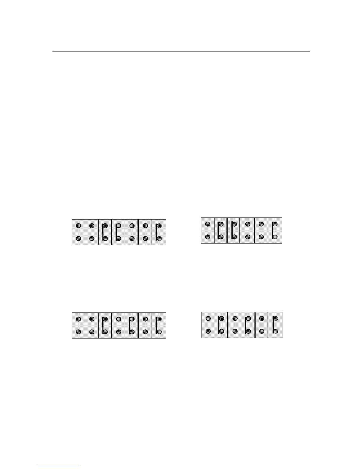
Each of the memory locations U2, U3, and U4 have a set of configuration jumpers. U2 has one
extra pair of jumper pins to manage both EPROMs and RAM. Standard settings configure all
locations for an 8K x 8 memory device. Alternative settings accommodate 64K x 8 (U2
Configuration Jumpers only), 32K x 8, and 16K x 8 devices.
MEMORY CONFIGURATION JUMPERS
Location: below each memory socket U2, U3, and U4( jumpers N, O, and P respectively).
2764, 2864, 6264
N-U2 8K x 8 O-U3, P-U4 8K x8
to Pin 1 to Pin 26 to Pin 27 to Pin 1 to Pin 26 to Pin 27
| | | x | x | | | x | | | x | x | | | x |
| | | x | x | | | x | | | x | x | | | x |
27128 EPROM
N-U2 16K x 8 O-U3, P-U4 16K x 8
to Pin 1 to Pin 26 to Pin 27 to Pin 1 to Pin 26 to Pin 27
| | | x | | x | | x | | | x | | x | | x |
| | | x | | x | | x | | | x | | x | | x |
Page 24
2/26/20022:06 PM2/26/2002
NMIY-0031 JUMPERS
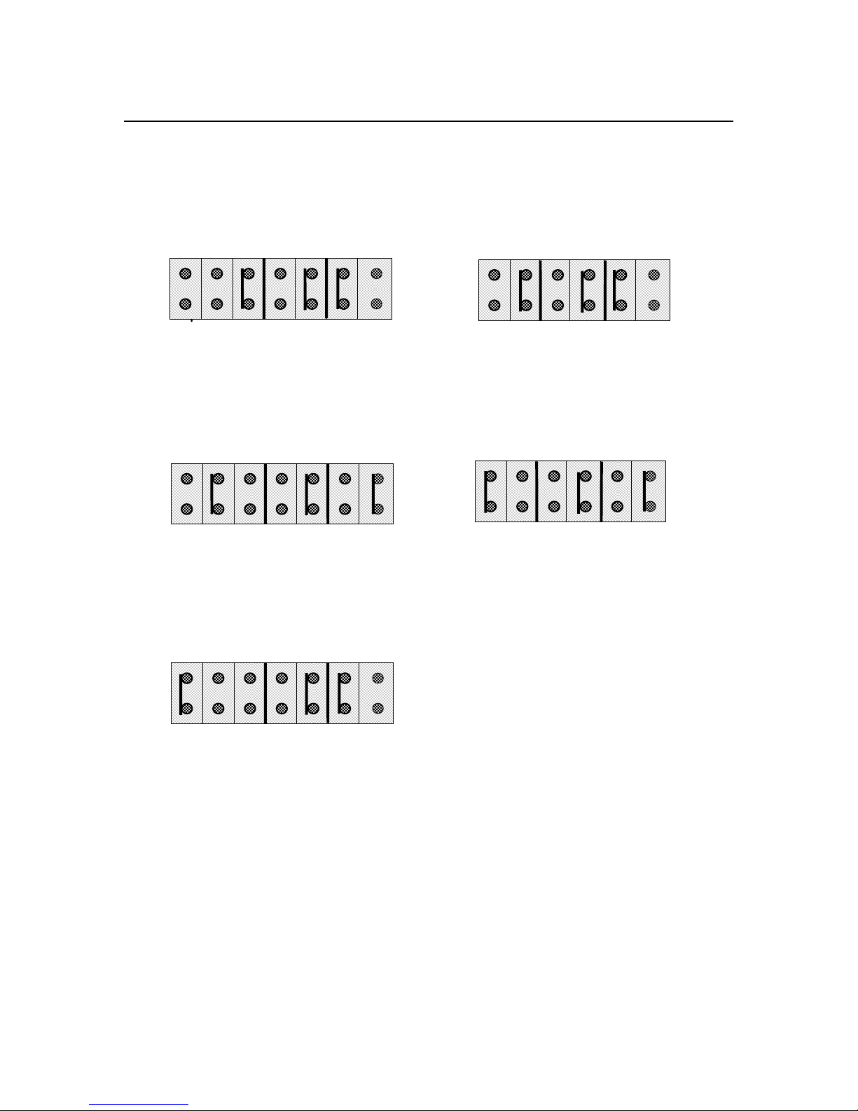
27256 EPROM
N-U2 32K x 8 O-U3, P-U4 32K x 8
to Pin 1 to Pin 26 to Pin 27 to Pin 1 to Pin 26 to Pin 27
| | | x | | x | x | | | | x | | x | x | |
| | | x | | x | x | | | | x | | x | x | |
62256 RAM
N-U2 32K x 8 O-U3, P-U4 32K x 8
to Pin 1 to Pin 26 to Pin 27 to Pin 1 to Pin 26 to Pin 27
24
| | x | | | x | | x | | x | | | x | | x |
| | x | | | x | | x | | x | | | x | | x |
27512 EPROM
N-U2 64K x 8
to Pin 1 to Pin 26 to Pin 27
| x | | | | x | x | |
| x | | | | x | x | |
H10, H11, and H12 configure U2, U3, and U4 respectively to allow RAM to emulate EPROM by
tying the WR* pin to VCC. To write protect RAM we recommend removal of the corresponding
jumper for pin 27 and installing a 100K resistor across the pins of H10, H11, or H12. With
battery backup in use, RAM emulates ROM.
RESET
Header Q, Located near J1 and J2, is reset. When shorted, reset is asserted. Q is normally open.
A typical developer would install a momentary switch at Q.
Page 25
2/26/20022:06 PM2/26/2002
NMIY-0031 JUMPERS
LCD CONTRAST
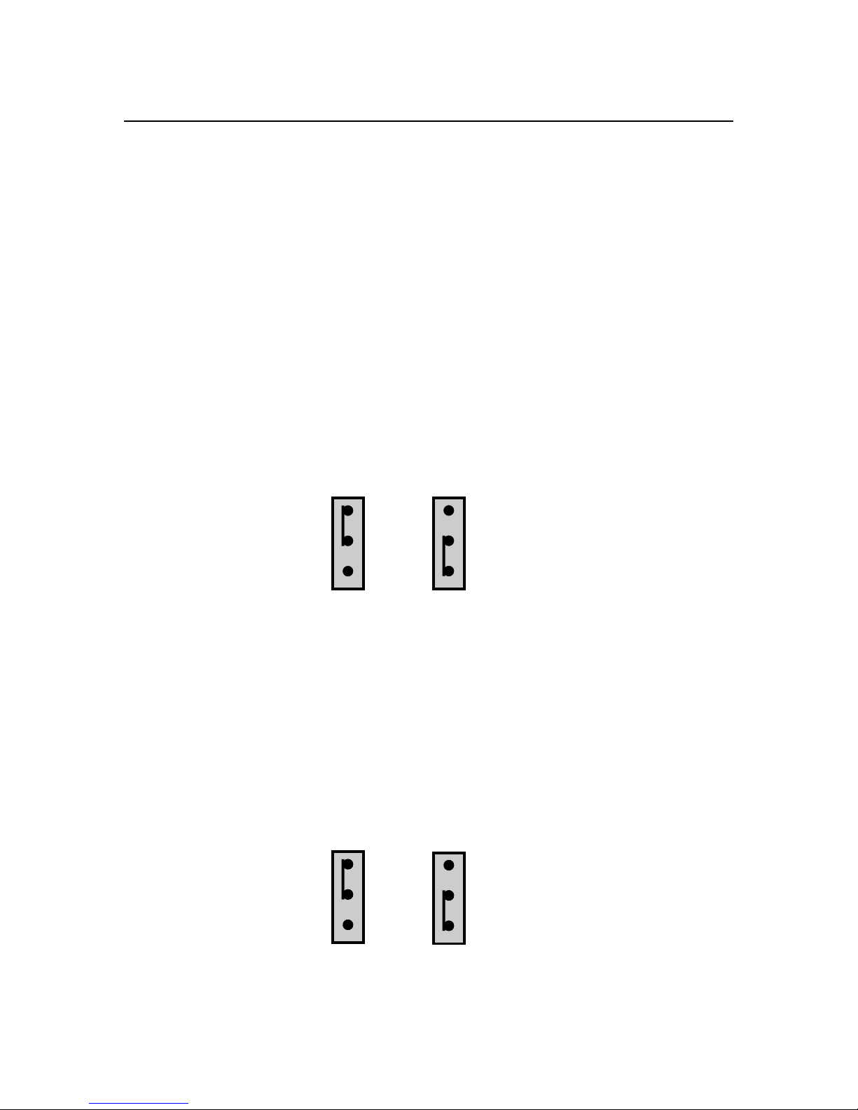
H1 provides contrast selection for the LCD display. Two ranges are available.
25
NOTE:
Three-pin configuration jumpers should be viewed from the component side of the
board with the prototype area positioned to the left. Pin 1 will be toward the top of the board,
and pin 3 will be toward the bottom of the board.
Location: Configuration headers H2 - H9 are located between the power supply section and U9
& 10.
H2, H3, and H4 configure memory locations U2 and U3. H2 selects data only(2-3) or code &
data(1-2) for U3. H3 selects code & data(2-3) or code only(1-2) for U2. Lastly, H4 selects 32K(1-
2) or 64K(2-3) for U2.
H4 H4
U2 32K U2 64K
1 x -
2 x x
3 - x
VERTICAL STACKING COMPONENT (VSC) CONFIGURATION JUMPERS
H5 selects an OE for the VSC connector J1 from either U2 or U3. See figure above.
H6 selects the interrupt for VSC connectors J1, J7, and J9. Interrupts 0 and 1 are available for
use. See figure below. All three VSC connectors J1, J7, and J9 share the same interrupt line.
H5 H5
OE-U2 OE-U3
for VSC for VSC
1 x -
2 x x
3 - x
Page 26
2/26/20022:06 PM2/26/2002
NMIY-0031 JUMPERS
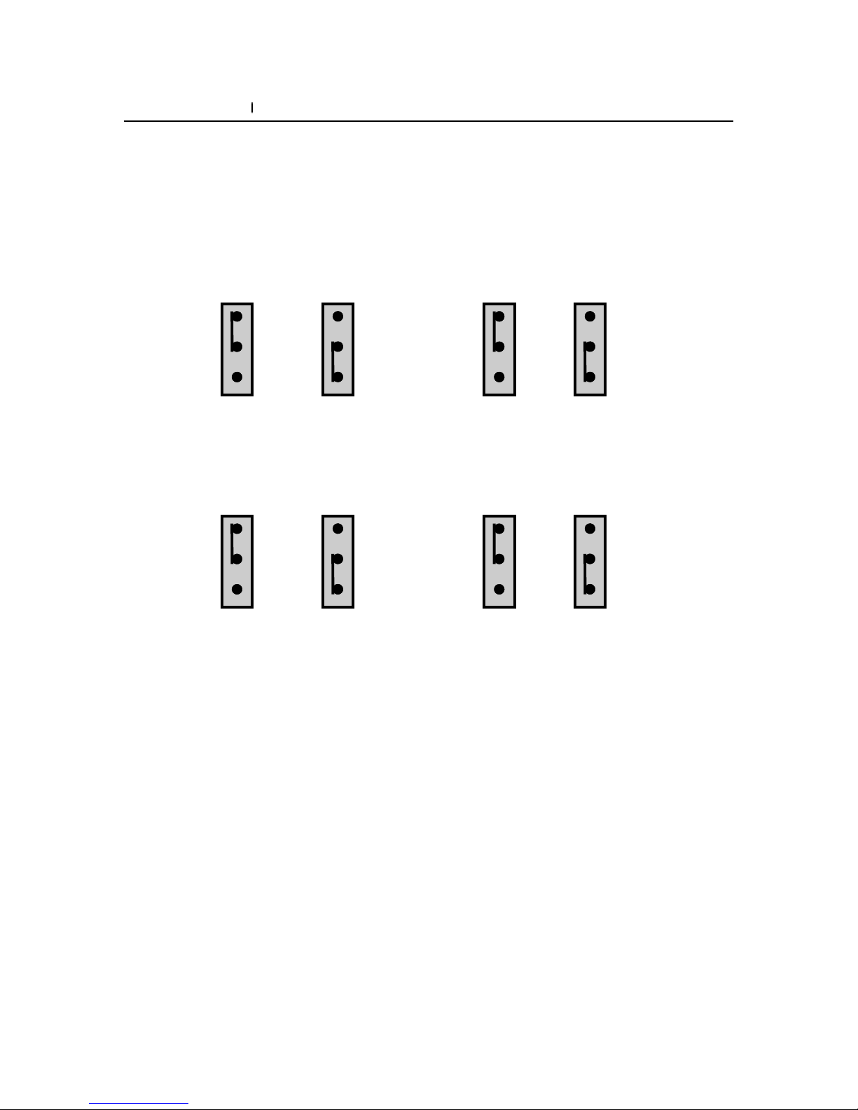
SERIAL COMMUNICATIONS CONFIGURATION JUMPERS
26
H7 and H8 select which serial format will be used for communications. H8 selects between
RS232 format and RS422/485. H7 and H9 select between RS422 and RS485. Standard
configuration uses RS232. Optional components must be installed for either RS422 or RS485.
H6 H6 H8 H8
int 0 int 1 RS232 RS422/RS485
1 x - x -
2 x x x x
3 - x - x
H7 H7 H9 H9
RS422 RS485 RS422 RS485
1 x - x -
2 x x x x
3 - x - x
Page 27

2/26/20022:06 PM2/26/2002
NMIY-0031 TROUBLESHOOTING
27
Troubleshooting
Every computer system requires certain resources to run. The immediate availability and
correctness of these resources should be checked first.. For a computer, these include:
• correct voltage, polarity, and regulation power supply
• a basic form of operating system
• RAM
• some form of user/application I/O
MOUNTING
Board mounting should be physically sturdy and electrically isolate all circuit traces from any
surrounding conductive surface. It is very important that no metal points on the board contact
external conductive items. We recommend nylon standoffs for mounting. See the section on
Board Mounting for mechanical details.
POWER SUPPLY
+5 VDC @ 250 mA is required at J12 for the standard version (be certain polarity is correct).
Boards with the power supply option require 6.3 to 10 VAC (alternatively +9 to +14 VDC) at
connector J2. Check for correct power in either version with a meter or scope at the screw
terminals of J12. When the supply is correct there will be + 5 VDC +/-5% with less than 80 mV
ripple (in either version) at J12. Use of an oscilloscope is recommended whenever there is a
question concerning power supply regulation.
OPERATING SYSTEM
Every CPU requires a base program to become functional. Such a program is usually referred to
as an operating system. Operating systems provide usability services for the user, and interface
directly with the hardware. The NMYI-0031 has four hardware-based operating system options:
BASIC, a Monitor, and FORTH in EPROM. There is also an optional PC based C cross
compiler that can be used to develop a base operating system and application. One of these or a
functional user supplied program, must be in location U2 with jumpers configured for the
memory type used to make the board operational. The type of EPROM installed in U2 must
match the settings of jumper block N. See the Jumpers for details.
Page 28

2/26/20022:06 PM2/26/2002
NMIY-0031 TROUBLESHOOTING
MEMORY
28
The program in U2 usually requires some read/write bus memory, or RAM, to function.
Locations U3 and U4 provide this function. An appropriate amount of memory should be
installed to satisfy the operating system and program requirements. BASIC and C require a
minimum of 8Kx8 in U3 to operate. FORTH requires 32Kx8 in both U3 and U4. Be sure to
check for any bent or broken pins on any devices installed in U2, U3, or U4. Occasionally such
checking will require removal of the device, but often a careful visual inspection will suffice.
TERMINAL
Useful computers require some form of input/output. Usually a human interface is desirable.
For the BASIC
FORTH, or Monitor options, an RS232 terminal or PC with terminal emulator is
,
typical. The RS2332 connector is J10. RS232 settings are 9600 baud, 8N1. J11 provides RS422
or 485 support when U12/13 are installed. Some RS232 terminal equipment requires support
lines as well as SO and SI lines. Check that your cable supports these lines if required. See the
I/O Connector
section to check your cable pinout. Remember to align pin 1 of J10 and your
cable. Pin 1 is the J10 pin closest to the corner of the board.
KEYPAD and LCD I/O
Keypad input requires program support. Keypad and LCD connectors are J3 and J6 respectively.
NMIY-0031 hardware supplies the necessary hardware control and data lines to make a keypad
and LCD interfaces electrically functional. FORTH
BASIC, Assembly, and C options each
,
provide some various levels of interface programmability.
PHYSICAL INSTALLATION OF DEVICES
On the physical side, all socket mounted components should be checked to ensure that:
• each chip is fully seated in its socket
• no pins are bent inward , outward, or curled under
• pin 1 of the device is mated with pin 1 of the socket(correct chip orientation)
• screw terminals are snugly fitted to the appropriate wires
• connectors are fully mated and properly oriented with respect to header pins
Additional product information is available at our world wide web site: www.newmicros.com
Support is available through our bulletin board by modem( 2400 maximum with 8-N-1) at: 214339-2321. If emergency support is required, contact us by phone at 214-339-2204.
Page 29

2/26/20022:06 PM2/26/2002
NMIY-0031 BOARD MOUNTING
29
Board Mounting
NMIY-0031 MOUNTING
Six mounting holes are provided for mounting the NMIY-0031. Each hole is drilled at 0.110
inches giving clearance for 4-40 hardware. Caution is necessary during installation to prevent
inadvertent grounding of printed circuit board traces. The mounting holes located near J4 and J6
have traces nearby. These are the holes near the center of the board’s long edges.
Common ¾ inch long hex standoffs with a male screw on one end and a female threaded hole on
the other are ideal inter-board connection devices. The VSC connector was designed to work
with this size spacer, giving reliable board to board mounting.
The standard spacer length, 0.750 inches, plus the board thickness, 0.061 inches, giving a nominal
board to board spacing of 0.811 inches. Should an exact spacing of 0.800 inches be required, as
in the case of standard mounting hardware having 0.800 inch PCB card guides, the standard
spacer will require milling to reduce its length by 0.011 inches.
VSC MOUNTING
The NMIY-0031 has connector pads for three VSC connectors. When these optional connectors
are installed, there are three sites for adding VSC cards. A VSC card plugs into the NMIY-0031
from above the component side of the board. The mounting holes for VSC cards are located in
‘ears’ along both long sides of the NMIY-0031 board. The projecting, mounting ears each extend
3/8 inch from the edge of the board. Connector lengths are designed to accommodate standard
¾ inch standoffs with a male screw on one end and a female threaded hole on the other.
The length of the standard spacer, .750 inches, plus the board thickness, .061 inches, gives a
nominal spacing board to board of .811 inches. When an exact spacing of .800 inches is desired,
(some standard mounting hardware have .800 inch mounting board guides), .011 inches of the
mounting surface at the female end of the soft brass standoff can be removed by mill or metal
file.
The extremely small size of the boards means there are no guaranteed limits on how close
components will be placed to the edge of the 2x4’s. Board guides will be difficult to use and
designs should take this into account. They may be acceptable if non-conductive and very
shallow. The main mounting holes are the best point of support.
Page 30

2/26/20022:06 PM2/26/2002
30
Page 31

2/26/20022:06 PM2/26/2002
NMIY-0031 SOFTWARE
31
PART III
SOFTWARE
The Software section supplies information for programming the NMIY-0031.
Programming gives information on program and data address spaces, and programming
locations and commands for hardware resources.
Program Segments provides sample program segments to illustrate use of commands to
hardware resources such as the keypad port and LCD interface. Program segments are provided
for Monitor, BASIC, C, and FORTH.
Page 32

2/26/20022:06 PM2/26/2002
32
Page 33

2/26/20022:06 PM2/26/2002
NMIY-0031 PROGRAMMING
Programming
Programmable board resources include interfaces for:
• latched 8 bit input and 8 bit output port
• raw (direct) 8 bit I/O port including:
• two interrupts
• two timer/event counters
• 4x5 keypad
• LCD
33
• serial data port
The 8031 processor has four memory mapped I/O ports; one is available to the user. Two ports
are required for bus address and data. The third port provides various signals: serial I/O, external
interrupts, timer/counter functions, and data space read/write. The fourth port is available to the
user. The eight lines of this port are available on J5.
The raw data port, interrupts, timer/counters, and serial port are implemented internally in the
8031. The other items are memory mapped to the processor externally by the board. The keypad
port is created with external logic. An additional port (latched) with eight inputs and eight
outputs is available at J4.
MEMORY
Three memory sockets are provided on the NMIY-0031. U2 is intended for the operating
system. Available items for U2 are BASIC, FORTH, and Monitor. A Small C compiler is also
available on diskette. Using C, the user can install an EPROM with a custom application
operating system for production. To support rapid development, electrically alterable devices
may be used in any of the three memory sockets to provide rapid development turnaround,
avoiding EPROM erase-reprogram cycling.
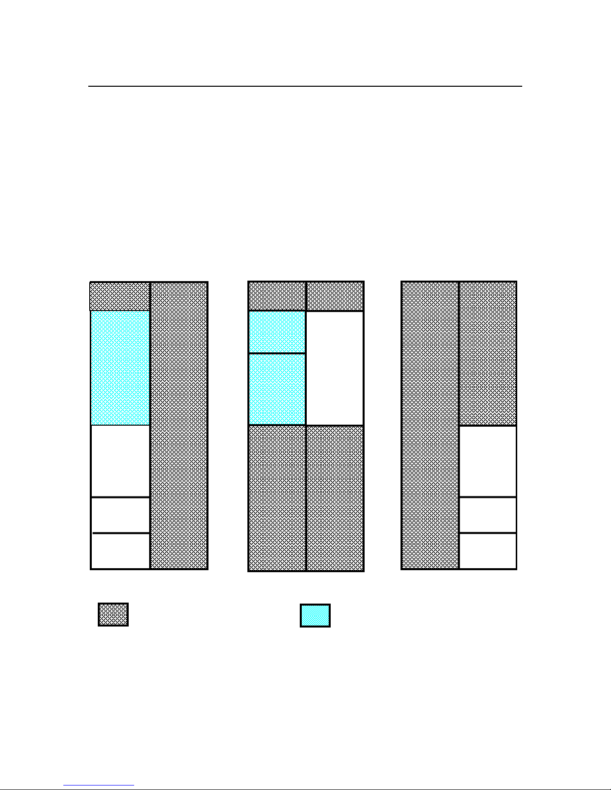
External memory address space on the 8031 is divided into two parts. A 64K program address
space and a 64K data address space. On the NMIY-0031 board, this distinction can be
maintained strictly by the user, or configured so that the two spaces overlap in U3.
U2 is mapped to the bottom of program memory space. For example, if an 8Kx8 EPROM is
installed then U2 is addressed from 0000 to 1FFF. Through configuration, U2 accepts up to 64K
of EPROM program space. See Jumpers for details.
Page 34
2/26/20022:06 PM2/26/2002
NMIY-0031 PROGRAMMING
34
U3 is configured as either program & data, or data only. The base address of U3 is 8000. When a
16Kx8 device is installed in U3, valid addresses range from 8000 to BFFF. H2 determines
whether U3 is addressed as program & data, or data only. Up to a 32Kx8 device may be used in
U3. See the Jumpers section for configuration details.
U4 is addressed as data only. The base address of U4 is 0000. Up to a 32Kx8 RAM may be used
in U4. A 32Kx8 RAM installed in U4 is addressed from 0000 to 7FFF as data.
ADDRESS SPACES
U2 U3 U4
Program Data Program Data Program Data
NNNN NNNN FFFF NNNN NNNN NNNN NNNN
NNNN NNNN NNNN NNNN FC00 NNNN NNNN
SSSAA NNNN SSSSSS SSSAA NNNN NNNN
SSSAA NNNN SSSSSS SSSAA NNNN NNNN
SSSAA NNNN SSSSSS SSSAA NNNN NNNN
SSSAA NNNN 7FFF SSSSSS SSSAA NNNN NNNN
AAAA NNNN NNNN NNNN NNNN AAAA
AAAA NNNN NNNN NNNN NNNN AAAA
AAAA NNNN 3FFF NNNN NNNN NNNN AAAA
AAAA NNNN NNNN NNNN NNNN AAAA
AAAA NNNN 1FFF NNNN NNNN NNNN AAAA
AAAA NNNN 0000 NNNN NNNN NNNN AAAA
NNN address space not available SSSS shared address space available
Page 35

2/26/20022:06 PM2/26/2002
35
NMIY-0031 PROGRAMMING
DATA PORTS
Two general purpose data ports are available. One port is an externally memory-mapped, latched
I/O port. The other is a raw (unprocessed) interface to processor Port 1.
LATCHED DATA PORT (J4)
The twenty pins of J4 contain latched input and output. These lines are an augmented alternative
to the keypad inputs on J3. All eight lines of both the read and write latches are available. The
latched data port and keypad use the same data latches. Please see the keypad information below
for programming details on the latches.
RAW DATA PORT (J5)
J5 gives the user access to Port 1 of the processor, timers 0 and 1, and interrupts 0 and 1..
Caution: be certain that any load/source attached meets the specifications of the 8031 processor.
Port 1 pins can source/sink up to four LSTTL loads. Excessive loads or signals can result in
processor failure. 8031 data books give timer and interrupt programming information.
The CSX signal is a chip select that maps to FExx in data space for both read and write. The user
can use this 256 byte memory block as desired, i.e. for custom memory mapped devices. The
lower eight address bits are available on the VSC connectors as needed. RST is the master board
reset used throughout the board.
Data lines on J5 are very useful for external control. The interrupts can be used to signal when
particular services are needed from the processor. The timer outputs/counter inputs are useful
for checking time dependent processes. Also, the direct data inputs are useful for bit oriented
input/output. These are a few suggestions for using the direct input/output connections. See an
8031/51A data book for details on timer, counter, and interrupt programming.
KEYPAD I/F
The NMIY-0031 keypad is designed to be used with a matrix type keypad. A matrix keypad
works by shorting together the corresponding row and column lines when a key is pressed. To
detect a key press, the program writes a value to the column data lines with the output latch. The
value sent out has a zero bit in the position corresponding to the column to be examined. The
row values, are then latched and examined. Software must determine which row and which
column are activated before the operator releases the key. Any column not pressed will return a
row value of FF. The column pressed will return a row value with a positional zero bit indicating
which key is pressed. Valid returns are FF, FE, FD, FB, and F7. See the “Program Segments”
chapter for examples.
The column-data latch address is FFFC. Writing to this address causes the data to be latched.
This latched byte is then available at J4 and the lower five bits (D4 - D0) are presented to the
column inputs of the keypad. The row data latch address is FFFC. Reading FFFC latches the
data of the four keypad row lines (D3 - D0). Until known data is latched onto the columns,
returned row data will be meaningless. See “Program Segments” for examples.
Page 36

2/26/20022:06 PM2/26/2002
36
NMIY-0031 PROGRAMMING
LCD I/F
The LCD interface is designed for a 2 or 4 row by 16, 20, or 40 character display. There are two
addresses for the LCD. One address is used for commands only and the second for display data
only. Commands are used to set the operating modes, clear the display, and set cursor position.
The recommended initialization sequence is 38, 38, 06, 0F, 01. The command address for the
LCD is FFF8. Command functions available are:
Clear Display is the command 01. When the value 01 is written to address FFF8, any data on
the display is removed and the cursor is returned to the home position. Data storage is cleared.
Cursor At Home is the command 02. The cursor is returned to the home position. Also the
display string being shifted is returned to the original position. Data storage is unchanged.
Entry Mode Set is a group of related commands. This group determines the cursor move
direction and specifies whether to shift the display. Each of these commands sets the mode used
when writing data to the LCD:
04 Move cursor to left.
Do not shift the display.
06 Move the cursor to the right.
Do not shift the display. (normal)
05 Move the cursor to the left.
Shift the display.
07 Move the cursor to the right.
Shift the display. (normal)
Display On/Off Control turns the display on or off as a whole, turns the cursor on or off, and
sets the cursor to blink or not.
08 Turn D, C, and B off 0C Turn D on, C and B off
09 Turn D and C off, B on 0D Turn D and B on, C off
0A Turn D and B off, C on 0E Turn D and C on, B off
0B Turn D off, B and C on 0F Turn D, B, and C on (normal)
where D is display, C is cursor, and B is blinking.
Note: The commands are hex numbers and are always upper case. It is recommended that the
terminal be set to
CAPS LOCK
on whenever hex numbers are to be entered.
Page 37

2/26/20022:06 PM2/26/2002
NMIY-0031 PROGRAMMING
37
Cursor/Display Shift moves the cursor and shifts the display without changing data. Cursor
move direction is also controlled.
10 Move cursor to the left 18 Shift data to left
14 Move cursor to the right 1C Shift data to the right
Function Set sets the number of display lines and selects character format.
30 Set 1 line display with
5x7 dot format.
34 Set 1 line display with
5x10 dot format.
38 Set 2 line display with 5x7 dot
format.
3C Set 2 line display with 5x10 dot
format.
DDRAM Address Set allows the cursor address to be manipulated.
1xxx xxxx binary
where x is a
binary digit
Character position addresses are:
80 to 8F(16) to 93(20) to A7(40) for the first line
C0 to CF(16) to D3(20) TO E7(40) for the second line
(Upper address limits are shown for 16, 20, and 40 character per line LCD’s)
Today most LCD’s use the same controller chip, the Hitachi HD44780, or equivalent, regardless
of display line length up to 40 characters and 4 lines. Data memory (DDRAM) will hold up to 40
characters on each line while displaying only a contiguous segment of that line equal to the
number of display characters. The position addresses are shown above where the 16, 20 and 40
character display line end addresses are noted. Note that these address limits assume that the first
character displayed is the first character of that line in memory. Using the shift feature, the first
character displayed can be moved within the memory space in DDRAM. For example, a 16
character per line display could display positions 98 to A7 when shifted fully to the right. See
Entry Mode Set for shift instructions. Addresses on each line wrap to the beginning of that line.
That is, A7 is adjacent to 80 and E7 is adjacent to C0. LCD’s with fewer than 40 characters per
line can still store a full 40 characters, but will display only 16 or 20 of them at a time. The display
window’s position will be the same for all lines of the display.
LCD’s have a command and a data address. The LCD data address is FFF9. When data is
written to this address it will be displayed according to the display mode previously selected.
Display characters are from an enhanced ASCII character set. Numerals, upper and lower case
roman letters, and punctuation marks are among the common characters supported.
Page 38

2/26/20022:06 PM2/26/2002
NMIY-0031 PROGRAMMING
38
Four line LCD’s use two controllers instead of the single one on 1 and two line models. To
access lines three and four, a second control line is provided for the second controller. The
second controller addresses are FFFA for commands and FFFB for data.
SERIAL I/O
Serial I/O is available through the 8031 processor’s serial port. For most users, the I/O routines
built into BASIC, FORTH, and C will support use of this port. See an 8031/51A data book for
details on assembly language usage.
Serial-interface, electrical format is determined by which chips among U11, U12, and U13 are
installed and the settings of jumpers H7, H8, and H9. See the section on Jumpers for particulars.
Page 39

2/26/20022:06 PM2/26/2002
NMIY-0031 PROGRAM SEGMENTS
39
Program Segments
The following examples are provided to display the process of communicating with the LCD and
key pad option. The code is written to be first instructive and secondly well written in the usual
sense. We assume that the user can produce well-written code after reading and understanding
the examples of using board facilities.
MONITOR
The following example will clear the LCD, set the display for blinking cursor on, and display the
message:
“HELLO WORLD!”
The monitor ignores embedded spaces in a command line. When the last numeral on each line is
entered the monitor will execute the command and give a new line at the control terminal. Note
that each line starts with an upper case “O” and all subsequent characters are valid hexadecimal
characters (all upper case) or spaces. The CAPS LOCK key is preferred. Spaces are not required
by the Monitor, but are allowed and included for readability. The comments on each line are
rejected by the monitor and should not be entered.
O 38 FFF8 ; Set 2 line display and 5x7 dot format
O 38 FFF8 ; Set 2 line display and 5x7 dot format
O 06 FFF8 ; Entry mode: cursor moves to right, no display shift
O 0F FFF8 ; Set display and blinking cursor on
O 01 FFF8 ; Clear Display
O 80 FFF8 ; Set cursor to left end of line one
O 22 FFF9 ; Display ‘ ” ’
O 48 FFF9 ; Display “H”
O 45 FFF9 ; Display “E”
O 4C FFF9 ; Display “L”
O 4C FFF9 ; Display “L”
O 4F FFF9 ; Display “O”
O 20 FFF9 ; Display “ “
O 57 FFF9 ; Display “W”
O 4F FFF9 ; Display “O”
O 52 FFF9 ; Display “R”
O 4C FFF9 ; Display “L”
O 44 FFF9 ; Display “D”
O 21 FFF9 ; Display “!”
O 22 FFF9 ; Display ‘ “ ‘
When the entry process is completed, you should see:
“HELLO WORLD!”_
on the LCD with a blinking cursor on the right end.
Keypad access is quite different. Reading is accomplished in a two step process. First, a column
value is written to the latch, then the latch is read. Successive column values are written and read
until a non-FF value is returned. This column is the one with a key press. The non-FF value
returned identifies the row value. The following example and explanation illustrates this:
Page 40

2/26/20022:06 PM2/26/2002
NMIY-0031 PROGRAM SEGMENTS
O FE FFFC ; Check column 1
D FFFC FE ; Read row
O FD FFFC ; Check column 2
D FFFC FF ; Read row
O FB FFFC ; Check column 3
D FFFC FF ; Read row
O F7 FFFC ; Check column 4
D FFFC FF ; Read row
O EF FFFC ; Check column 5
D FFFC FF ; Read row
40
Each of the
D FFFC
commands returns a two digit hex value corresponding to the key pressed.
The column value scanned when a non-FF return occurs, indicates the column pressed. Valid
return values are FE, FB, FD, and F7. When a key in row 1 is pressed, then the one bit is
returned as zero, FE. Row 2 returns FB, row 3 returns FD, and row 4 returns F7. The value
returned by any other column will be FF.
EXAMPLE
If the key in row 3, column 2 is pressed, then after entering:
O FD FFFC
D FFFC FB
the value FB is returned, while all other columns will return FF. The FB hex return value
signifies a row 2 key is pressed. Bit 2 of FB has a zero value which identifies the row as 3.
Remember to hold the key-pad key down while entering the “ D “ commands. If row 1 has a
key pressed, the return value will be FE, row 2 would return FD, row 3 FB, and row 4 F7.
Whenever a D command returns a value other than FF, the row pressed is determined by
examining the return value.
The examples that follow assume use of a 4 line by 40 character LCD, and a 4 row by 5 column
keypad. If other device configurations are used, it will be necessary to adjust either some values
or interpretations of results.
Page 41

2/26/20022:06 PM2/26/2002
NMIY-0031 PROGRAM SEGMENTS
BASIC
41
The following example clears and resets the LCD, and then displays the coordinates of the key
press on the matrix keypad. The LCD and key pad interfaces are mapped into external data
memory. BASIC uses the XBY() function to access external memory. Memory mapped facilities
such as the built-in LCD and keypad interfaces or an NMIL add-on board can be accessed using
XBY(adr, [data]). The keypad is addressed at 0FFFCH and the LCD (up to 4x20 display) is
addressed at 0FFF8/9H as detailed below. A 4 line by 40 character LCD will require addresses
0FFFA/BH also, for the second control processor on the LCD.
The LCD will display the coordinates of the last key pressed on the keypad when the following
code is executed. The code is organized to show the distinct functions necessary to initialize and
control the LCD and keypad. First, the keypad, LCD, and string array are initialized. Then a
keypad scan is executed until a key press is detected. The specific coordinates are then
determined and written to the next line on the LCD. The keypad scan is then resumed until
another key is pressed.
NEW
10 STRING 22,20 :REM Allocate string space
20 I = 0
22 ROW = 0 :REM Initialize row and column indices
24 COL = 0
REM Constants
30 KEYPAD = 0FFFCH :REM Keypad latch write/read address
32 LCDCMD = 0FFF8H :REM Display command address
34 LCDDAT = 0FFF9H :REM Display data address
35 LCDLINE = 20 :REM Display line length
36 NUMROWS = 4 :REM Number of display rows
37 NUMCOLS = 5 :REM Number of display columns
40 DIM B(5) :REM Declare array
100 GOSUB 1100 :REM Initialize the LCD
REM Start scan loop
110 DO
120 FOR I = 1 TO 5 :REM Scan columns for key press
130 XBY(KEYPAD) = B(I) :REM Output column data
140 KPDAT = XBY(KEYPAD) :REM Read row data
REM Save key-press values and exit
150 IF KPDAT <> 0FFH THEN COL = I : ROW = KPDAT : I = 5
160 NEXT I
170 UNTIL ROW <> 0 :REM Loop until key-press
REM De-bounce key-press
200 DO : KPDAT = XBY(KEYPAD) : WHILE (KPDAT = ROW )
REM Convert row value to coordinate
210 FOR I = 1 TO NUMROWS
220 IF B(I) = ROW THEN ROW = I
230 NEXT I
REM Assemble display string
300 ASC($(0), 1) = ROW + 030H
310 ASC($(0), 2) = 02CH :REM comma
320 ASC($(0), 3) = 020H :REM space
330 ASC($(0), 4) = COL + 030H
400 GOSUB 1000 :REM Write key position to display
Page 42

2/26/20022:06 PM2/26/2002
NMIY-0031 PROGRAM SEGMENTS
450 GOTO 110 :REM Loop until console CTRL-C
500 END
REM Write key position to display
1000 XBY(LCDCMD) = 01H :REM Clear display and return home
1010 FOR I = 1 TO LCDLINE
1020 XBY(LCDDAT) = ASC($(0), I) : NEXT I
1030 COL= 0 : ROW = 0
1040 RETURN
REM INITIALIZATION INSTRUCTIONS
REM Initialize Array
1100 B(1) = 0FEH :REM Initialize column address vector
1110 B(2) = 0FDH
1120 B(3) = 0FBH
1130 B(4) = 0F7H
1140 B(5) = 0EFH
REM Initialize Display
1200 XBY(LCDCMD) = 038H :REM Get attention
1210 XBY(LCDCMD) = 038H :REM Set 2 line display and 5x7 dot format
1220 XBY(LCDCMD) = 006H :REM Entry mode: cursor to right, no shift
1230 XBY(LCDCMD) = 00FH :REM Set display and blinking cursor on
1240 XBY(LCDCMD) = 001H :REM Clear Display
REM Clear string array
1300 FOR I = 1 TO LCDLINE
1310 ASC($(0), I) = 020H : NEXT I
1320 RETURN
42
Page 43

2/26/20022:06 PM2/26/2002
NMIY-0031 PROGRAM SEGMENTS
C
The example segment for C does the same function as the
BASIC
example above. First the key-
43
pad is read until a key press is detected. The key press coordinates are determined and then
output to the LCD.
#include ..\clib\common51.c
#include ..\clib\syslib51.c
#include ..\clib\stdio.h
#include ..\clib\alloc.c
#include ..\clib\peekpoke.c
#include ..\clib\getchar.c
#include ..\clib\fgetc.c
main ()
{
char *ch1;
int coldata,
row, col;
_lcdinit();
_lcdbusy();
while (EOF)
{
coldata = 1;
col = 0;
row = 0;
for (col = 1; col < 6; col++) /* scan columns */
{
_kpad_put(coldata ^ 0xFF); /* output column bit */
if (row = _kpad_get(ch1)) /* check for key press */
{
while
(row == _kpad_get(ch1)); /* de-bounce key press */
_lcdhome();
_dispdata(row, col); /* display key press */
}
else
coldata = coldata << 1;
} /* end for */
} /* end while */
} /* end main */
_dispdata(row, col) /* output data to lcd */
int row, col;
{
if ( row == 0x0004)
row = 3;
else if ( row == 0x0008)
row = 4;
lcdput(row+0x0030);
lcdput(',');
lcdput(col+0x0030);
lcdput(' ');
}
Page 44

2/26/20022:06 PM2/26/2002
NMIY-0031 PROGRAM SEGMENTS
_kpad_put(ch) /* write to keypad latch */
char ch;
{
int *adr;
adr = 0x0FFFC;
_lcdbusy(); /* wait */
pokeb(adr, ch); /* send character */
return(ch);
}
_kpad_get(ch) /* read keypad latch */
char ch;
{
int *adr;
adr = 0xFFFC;
ch = (peekb(adr) ^ 0x00FF);
return(ch);
}
_lcdbusy () /* wait for LCD not busy */
{
int *adr;
adr = 0x0FFF8;
while (peekb(adr) & 0x0080);
}
_lcdput(ch) /* write display data to LCD */
char ch;
{
int *adr;
adr = 0x0FFF9;
_lcdbusy(); /* wait */
pokeb(adr, ch); /* send character */
}
_lcdcr() /* set LCD cursor to other line */
{
char z;
int i,
*adr;
_lcdbusy();
/* compute other line address */
adr = 0xFFF8;
z = peekb(adr) & 0x0040 ^ 0x00C0;
pokeb(adr, z); /* set cursor at BOL */
for (i=0; i++; i<40) /* clear to LCD EOL */
{
_lcdput(' '); /* clear next position */
_lcdbusy(); /* wait */
}
pokeb(adr, z); /* reposition cursor */
}
44
Page 45

2/26/20022:06 PM2/26/2002
NMIY-0031 PROGRAM SEGMENTS
_lcdhome() /* set LCD cursor at home position */
{
int *adr;
adr = 0xFFF8;
_lcdbusy();
pokeb(adr, 0x0001);
}
_lcdinit() /* reset LCD display */
{
int *adr;
adr = 0xFFF8;
_lcdbusy(); /* wait */
pokeb(adr, 0x0038); /* get attention */
_lcdbusy();
pokeb(adr, 0x0038); /* 8 bit data, 2 lines, 5x7 dots */
_lcdbusy();
pokeb(adr, 0x0006); /* cursor inc, no display shift */
_lcdbusy();
pokeb(adr, 0x000F); /* display on, blinking cursor on */
_lcdbusy();
pokeb(adr, 0x0001); /* clear display, set cursor to home */
}
45
Page 46

2/26/20022:06 PM2/26/2002
NMIY-0031 PROGRAM SEGMENTS
FORTH
( GENERIC KEYPAD INPUT AND LCD OUTPUT ROUTINES
( -----
HEX
( LCD DISPLAY ROUTINES
( -----
0FFF8 CONSTANT DSP-CMD
0FFF9 CONSTANT DSP-DATA
0FFFC CONSTANT KPAD
5 CONSTANT TOT-COL
4 CONSTANT TOT-ROW
VARIABLE COL
VARIABLE ROW
: WAIT-NOT-BUSY BEGIN DSP-CMD C@ 080 AND 0= UNTIL ;
: DSP-CLEAR WAIT-NOT-BUSY 01 DSP-CMD C! ;
: DSP-HOME WAIT-NOT-BUSY 02 DSP-CMD C! ;
028 CONSTANT DC/L
( position cursor on top 00-27 or bottom 28-4F line -- 2x40 DISPLAY
: DSP-AT ( n -- )
DUP DC/L MOD 080 OR SWAP DC/L 1- > IF 040 OR THEN
WAIT-NOT-BUSY DSP-CMD C! ;
( return cursor position
: C-URSOR? ( -- n )
WAIT-NOT-BUSY DSP-CMD C@ 07F AND ;
( print a character, move cursor to left
: DSP-EMIT ( char -- ) WAIT-NOT-BUSY DSP-DATA C! ;
( print a string on the LCD, writes past end of line.......
: DSP-TYPE ( addr n -- )
?DUP IF 0 DO COUNT DSP-EMIT LOOP THEN DROP ;
( init the display
: DSP-ON
WAIT-NOT-BUSY
038 DSP-CMD C! ( get attention )
038 DSP-CMD C! ( set 2 line display, 2x40 )
06 DSP-CMD C! ( character entry right )
0F DSP-CMD C! ( display & cursor on, blinking )
01 DSP-CMD C! ( clear display, set cursor home )
;
( COMPILE NON-PRINTING STRINGS
( -----
: (")
R@ COUNT DUP 1+ R> + >R ;
: "
COMPILE (") 022 WORD C@ 1+ ALLOT ; IMMEDIATE
: DSP-SPACES ( n -- )
?DUP IF 0 DO BL DSP-EMIT LOOP THEN ;
46
Page 47

2/26/20022:06 PM2/26/2002
NMIY-0031 PROGRAM SEGMENTS
: (D.) ( d -- addr # )
SWAP OVER DABS <# #S SIGN #> ;
: DSP-D. ( d -- )
(D.) DSP-TYPE BL DSP-EMIT ;
: DSP-D.R ( d n -- )
>R (D.) R> OVER - 0 MAX DSP-SPACES DSP-TYPE ;
: DSP-. ( n -- ) S->D DSP-D. ;
: TEST
DSP-ON
DSP-CLEAR " THIS IS A TEST " DSP-TYPE ;
: 2** ( input X 0-F --- OUT 2**X
1
BEGIN
OVER ( 0= NOT
WHILE
SWAP
1 SWAP
2*
REPEAT
SWAP DROP
;
( read keypad latch
: KPAD? ( -- n ) KPAD C@ FF XOR ;
( write to keypad latch
: KPAD! ( n-- ) KPAD C! ;
( detect keypress
: ?KPAD ( -- row# ) 0 KPAD! BEGIN KPAD? UNTIL KPAD? ;
( determine which row and column are pressed
( values are saved in variables ROW and COL
: SCAN
0FFFF ROW !
0FFFF COL !
TOT-COL 0
DO
I 2** 0FF XOR
KPAD!
TOT-ROW 0
DO
KPAD? I 2** AND IF I ROW ! J COL ! THEN
LOOP
LOOP
;
: CONVERT-KPAD ( ROW COL -- n ) (map key coordinates to single ASCII character
ROW @ TOT-COL * COL @ +
DUP 04 = IF DROP 017 ELSE ( convert unlabeled keys
DUP 09 = IF DROP 018 ELSE
DUP 0E = IF DROP 019 ELSE
DUP 013 =
IF DROP 01A THEN THEN THEN THEN ( bias #s and letters
DUP 017 <
IF DUP 03 > IF 1- DUP 07 > IF 1- DUP 0B > IF 1- THEN THEN THEN THEN
DUP 09 > OVER 017 < AND
IF 07 + THEN
030 +
;
47
Page 48

2/26/20022:06 PM2/26/2002
NMIY-0031 PROGRAM SEGMENTS
( detect key press
: KPAD-PRESS?
BEGIN SCAN COL @ ROW @ AND 0FFFF = NOT UNTIL
;
( de-bounce key pad
: KPAD-RELEASE?
COL @ 2** 0FF XOR KPAD! BEGIN KPAD? ROW @ 2** AND 0= UNTIL
;
( get and de-bounce key press
: GET-KPAD
KPAD-PRESS?
CONVERT-KPAD
KPAD-RELEASE?
;
( get key press and display on LCD
: KPAD>DSP
DSP-ON
BEGIN
GET-KPAD
DSP-EMIT
?TERMINAL
UNTIL
;
DECIMAL
48
Page 49

2/26/20022:06 PM2/26/2002
NMIY-0031 PART IV DRAWINGS
49
PART I V
DRAWINGS
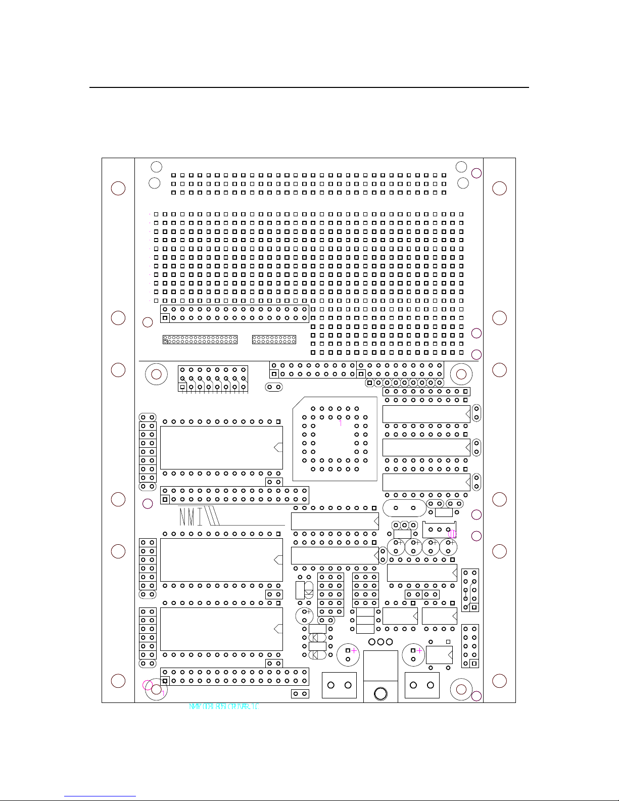
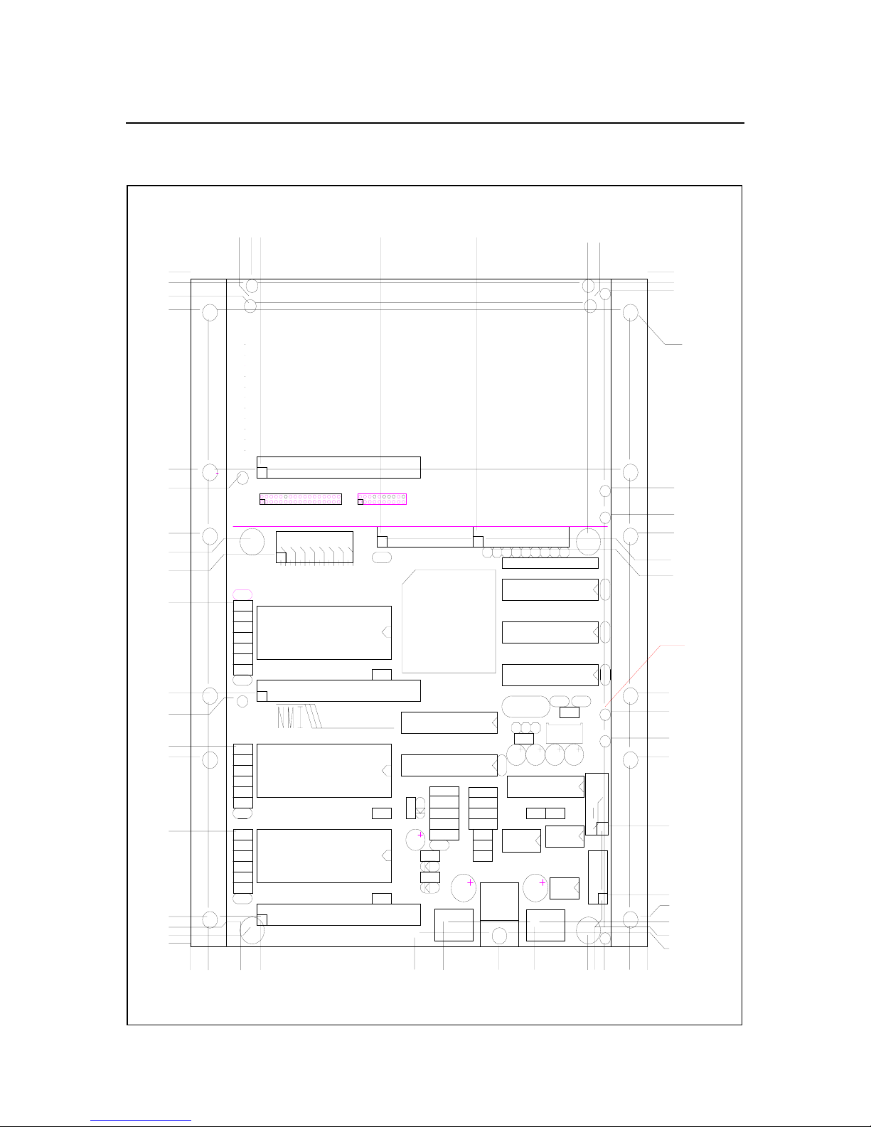
The Drawings section contains the parts list, silk screen for the board, mechanical detail drawing,
and board schematic.
Page 50

2/26/20022:06 PM2/26/2002
50
Page 51

2/26/20022:06 PM2/26/2002
NMIY-0031 PARTS LIST
51
Parts List
Component Location Component Location
Capacitor, 0.1 uF C1, 5-9, 12, 17-18 IC, 74HC573 U8
Capacitor, 22 pF C2-4 IC, SN75176 U12-13
Capacitor, 10 uF C10, 13-16 80C51A U1
16V electrolytic Jumper pin double
Capacitor, 100 uF C19-20 Jumper pin single
16V electrolytic PCB, NMIY-0031 BOARD
Connector 34 pin VSC, J1 Resistor, 1K, 5%, ¼ W R8
dual row header Resistor, 4.7K, 5%, ¼ W R2-3
Spacer 34 pin VSC Resistor, 10K, 5%, ¼ W R5-7,9
Diode, 1N4148 D1-3 Resistor, 10K, 10P9E RN1
Bridge rectifier, DB101 CR1 Resistor, 10K, pot. R4
Regulator, 7805 VR1 Resistor, 10M, 5%, ¼ W R1
IC, GAL16V8 U9-10 Socket, 8 pin U12-13
IC, MAX232 U11 Socket, 16 pin U11
IC, 8K BASIC EPROM U2 Socket, 20 pin U5, 6, 8, 9, 10
IC, 8K MONITOR U2 Socket, 28 pin wide U2-4
IC, HY6264ALP-12 U3 Socket, 44 pin PLCC U1
IC, 74HC245 U5 Shunt various
IC, 74HC273 U6 Terminal, 2 pin, screw down J2, 12
XTAL, 11.053 Y1
Page 52

2/26/20022:06 PM2/26/2002
52
Page 53
2/26/20022:06 PM2/26/2002
C10
J3
C6
1
N
NMIY-0031 SILK SCREEN
Silk Screen
APF04
J7
53
J5
J5
74HC245
8051
74HC573
74HC273
J9
O
PAL/GAL16V8
R3
R4
PAL/GAL16V8
U3
MAX232
R7
P
H11
U4
R8
R6
R5
S2 S1
75176
75176
R2
D1
R9
C20
VR1
CR
VM 08
-
-
-
D3
J12
LM780
C19
J2
J11
-
Page 54

2/26/20022:06 PM2/26/2002
54
Page 55
2/26/20022:06 PM2/26/2002
NMIY-0031 MECHANICAL DRAWING
Mechanical Drawing
55
6.300
6.200
6.012
5.950
4.450
4.400
3.850
3.800
3.650
3.200
2.350
2.300
1.850
1.750
0.604
0.625
0.725
2.9751.975
ϑ
74ΗΧ2
805
ΠΑΛ/ΓΑΛ
ΠΑΛ/ΓΑΛ
Υ
74ΗΧ5
74ΗΧ2
Ψ
Ρ3
ΜΑΞ
4.1454.125
6.300
6.200
6.125
0.156∀
12
4.275
4.025
3.850
3.800
3.700
0.110∀
17
2.350
Ρ1
2.175
1.925
1.750
1.050
0.250
0.200
0.150
0.000
0.000 0.187
0.250 2.325 2.628 3.200 3.575
0.200
4.750
1.100
0.450
0.250
0.200
0.150
Χ
Ρ2
∆
Ρ8
7517
Ρ6
Ρ5
7517
4.275
4.125
4.300
4.563
Page 56

2/26/20022:06 PM2/26/2002
56
Page 57
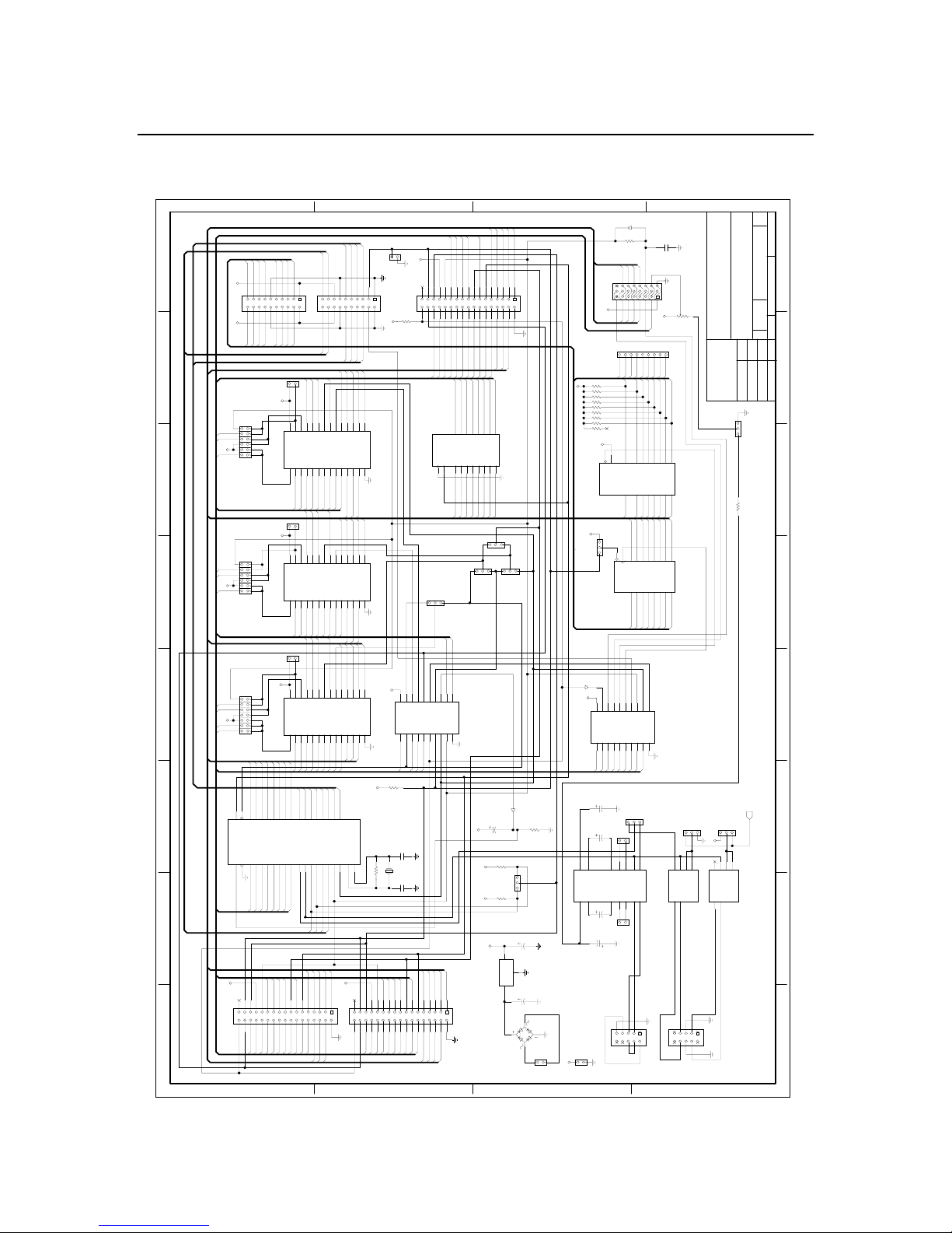
2/26/20022:06 PM2/26/2002
9
N
R
NMIY-0031 SCHEMATIC
Schematic
57
1
PB.6
+5V
CONTROL SIGNALS
+5V
J4
PORT B
PORT 1
DATA BUS
ADDRESS BUS
PB.7
WR
P
A14
A13
+5V
A14
3
O
WR
A14
A13
+5V
PORT 1
4
A14
DATA BUS
ADDRESS BUS
CONTROL SIGNALS
PA.6
PB.0
PB.2
PB.4
101214161820
PA.7
PB.1
PB.5
PB.3
PA.4
PA.0
PA.2
135791113151719
2468
PA.3
PA.1
PA.5
12
H12
A8
+5V
A8A9
+5
U4
123456789
A6
A7
A12
12
H11
A8
+5V
A8A9
+5
U3
123456789
A6
A7
A12
T0
INT0
INT1
T1
RD
A9
A11
A10
OE
A11A10
A5
A2
A4
A3
A11
A9
A10
OE
A11A10
A5
A2
A4
A3
RST
P1.2
P1.6
P1.0
P1.4
101214161820
P1.1
P1.3
P1.5
P1.7
CSX
D5
D4
D6
D7
D3
CS-U4
1516171819202122232425262728
CSD7D6D5D4D3
GNDD2D1D0A0A1A2A3A4A5A6A7A12
1011121314
A0
A1
D1
D2
D0
D5
D4
D6
D7
D3
1516171819202122232425262728
CSD7D6D5D4D3
GNDD2D1D0A0A1A2A3A4A5A6A7A12
1011121314
A0
A1
D1
D2
D0
1
Q
2
135791113151719
J5
2468
R9
10K
+5V
CS-U4
RD
WR
CSX
MEMORY
WR
CSX
OE-U2
MEMORY
+5V
INT
RST
A13
A9
A8
+5V
WR
NC
12
E
A6
A5
A7
A14
A15
A12
MEMDIS
A0
A2
A1
1918171615141312
1Q2Q3Q4Q5Q6Q7Q8Q
U8
11123456789
ALE
D1
D2
D0
H3
U2
U4:32K DATA
H4
123
64K32K
OE
A11
A10
D5
D4
D6
D7
ALE
10121416182022242628303234
A0
A2
A1
A4
A3
D1
D2
D0
A6
A5
A7
A4
A3
74HC573
8D7D6D5D4D3D2D1DCOC
D5
D4
D6
D7
D3
123
H5
123
123
H2
PSEN
PROGRAM
PROG/DATA
U2
D3
13579111315171921232527293133
J1
2468
WR
DATA
U3
PSEN
WR
RD
BCD
+5V
MEMDIS
E
RST
INT
VSC-OE
ALE
MEMDIS
E
RST
INT
VSC-OE
ALE
D1
12
12
C4
12
R2
4.7K
D4
D6
D2
D0
VO
WR1
NC
12
15
18
21
24
9
6
3
8
5
2
11
14
17
20
23
DATA BUS
ADDRESS BUS
+5V
E2
J3
123456789
PB.0
12
13
15
18
1
10
+5V
RN116RN1
RN1
RN1
RN1
RN114RN119RN117RN1
191 2 3456789
G
DIR
U5
+5V
1
2
J8
11 134781 3141718
3
CLR
U6
J6
7
4
1
10
13
16
19
22
A0
E1
D5
D7
D3
D1
+5V
X4X3X2 Y5Y4Y3Y2Y1 X1
PA.3
PA.1
PA.0
PA.2
PB.1
PB.2
PB.4
PB.3
PA.6
PA.5
PA.4
PA.3
PA.1
PA.0
PA.2
A1A2A3A4A5A6A7A8
B1B2B3B4B5B6B7B8
1817161514131211
D3
D2
D0
D1
D5
D6
D7
D4
D5
D6
D7
D4
D3
D2
D0
D1
1D2D3D4D5D6D7D8D
CP
1Q2Q3Q4Q5Q6Q7Q8Q
2569
12151619
PB.6
PB.1
PB.0
PB.2
PB.5
PB.4
PB.3
PB.7
123
PA.7
A
22pF
LCD CONNECTO
R4
10K
connector
4x5 Keypad
74HC245
NMIY-00
TITLE
DATE
051496
GLM
CIBI-ARDY
APPROVA
DRAWNCHECK
3
2
H1
1
1
R3
4.7K
2
IO@RD
IO@WR
74HC273
1
REV
1 OF
SHEE
1
APF05
DWG
D
SCAL
SIZE
0514
22
JRG
3
4
EFINI
12
WR
5
6
A14
A13
+5V
A14
A15
3332
ALE
U1
7
+5V +5V
J9
8
DCB
H10
D5
D4
D6
D7
A9
A8
A11
A10
OE-U2
N
1314
1112
9
10
78
56
34
12
D2
D0
D1
D3
+5V
U2
D5
D4
D6
A8A9
OE
+5
A11A10
123456789
A6
A5
A7
A4
A3
A12
D7
P1.1
P1.3
P1.2
P1.0
P1.5
P1.4
CS-U2
CSD7D6D5D4D3
1011121314
A0
A2
A1
D1
D2
D0
P1.6
P1.7
434241403938373623456789
P0.0P0.1P0.2P0.3P0.4P0.5P0.6P0.7P1.0P1.1P1.2P1.3P1.4P1.5P1.6P1.7
PSEN
EARESET
242526272829303111131415161718191035
A11
A13
A12
A9
A8
A13
A6
A5
A7
A14
INT0
A15
TXDTTL
RXDTTL
D7
VSC-OE
ALE
A11
A10
10121416182022242628303234
A0
A2
A1
A4
A3
A9
A8
A10
WR
INT
RST
+5V
A14 A14
A15 A15
A12 A12
E
MEMDIS
T0
WR
T1
INT1
D5
D6
D4
D3
13579111315171921232527293133
2468
D2
D0
D1
XTAL2XTAL1P3.7P3.6P3.5P3.4P3.3P3.2P3.1P3.0P2.7P2.6P2.5P2.4P2.3P2.2P2.1P2.0
2120
RD
J7
E
MEMDIS
D3
+5V
1516171819202122232425262728
VCC
I/O7I/O6I/O5I/O4I/O3I/O2I/O1I/O0
U10
MEMORY
GNDD2D1D0A0A1A2A3A4A5A6A7A12
123456789
A12
PSEN
+5V
12
1K
R8
8051
C2
10M
11.0592MHz
12
2
1
Y1
R1
1
2
C3
12
A9
A8
WR
INT
VSC-OE
RST
A11
A13
+5V
A6
A5
A7
A4
A3
P/DATA
CSI/O
CS-U4
CS-U3
E
RST
A14
A15
A13
RD
MEMDIS
22pF
RD
RST
RST
MEMDIS
22pF
D5
D6
D7
D4
ALE
A10
2468
10121416182022242628303234
A0
A2
A1
D2
D0
D1
A11
A10
11121314151617181920
G/OE
GNDI8I7I6I5I4I3I2I1IO/CK
PAL/GAL16V8
10
WR
2
1
C10
10uF
+5V
12
+5V
ALE
TXDTTL
RXDTTL
VSC-OE
R5
R6
+5V
12
+5V
VR1
LM7805
12
H6
10K
3
OUT
IN
1
WR
D3
13579111315171921232527293133
D2
1N4148
R71210K
3
2
1
12
GND
2
C19
100uF
12
6
3
1
4
CR1
12
J2
U11
C20
100uF
+5V
D3
E2
E1
IO@RD
12
+5V
VCC
U9
IO/CKI1I2I3I4I5I6I7I8GND
123456789
A5
A2
A1
A4
A3
C14
10uF
12
C13
10uF
S2
12
12
123
C1+V+C1-
C2+V- C2-
564
1413
12
12
C16
10uF
12
C15
10uF
10
12
NCNC
J12
RD
WR
CSX
CSI/O
IO@WR
11121314151617181920
I/O0I/O1I/O2I/O3I/O4I/O5I/O6I/O7
G/OE
PAL/GAL16V8
10
A9
A8
A6
A7
H8
123
9101211
1234
R2OT2I
R1OT1I
U12
R2I
R1I
T2OT1O
MAX232CWE
78
67
S1
-485XCV+422RCV
SI
SO
NC
123456789
J10
10
DI
RO
BA
485422
REDE
H7
123
123
+5V
1234
DI
REDE
RO
U13
BA
67
-422XMT
+422XMT
123456789
J11
A
P1.7
H9
5
6
7
8
Page 58

2/26/20022:06 PM2/26/2002
58
Page 59

2/26/20022:06 PM2/26/2002
59
APPENDICES
The appendices included contain example code using various NMIL series cards. These cards
provide extended functionality for the NMIY-0031. NMIL cards attach to the NMIY-0031
processor card through the vertical stacking connectors (VSC). The NMIY-0031 has three VSC
connectors for adding up to three cards in low profile. The VSC connection system can accept
many more than three cards, however, since each NMIL card also has a VSC. Cards using the
VSC system may be added to a stack as needed until bus loading becomes an issue.
Sample code is included in BASIC, C, and FORTH for:
• LCD and Keypad interfaces on NMIY-0031
• NMIL-1055 24-BIT I/O board
• NMIL-3003 64 Input HC compatible board
• NMIL-3004 64 Output HC compatible board
• NMIL-4000 8-Channel, 8-Bit, Digital-to-Analog board
• NMIL-4004 1-Channel, 12-Bit, Analog-to-Digital board
• NMIL-5000 ACIA 1-Channel Serial Communications board
• NMIL-7001 16-Channel OPTO Isolator Output board
• NMIL-7003 8-Channel Input, 8-Channel Output OPTO Isolator
board
• NMIL-7022 8-Channel, Mechanical Relay (SPST) board
• NMIL-7040 4-Channel Stepper Motor Controller board
• NMIL-7056 Servo Motor Driver board
• NMIL-9003 Real Time Clock board
Page 60

2/26/20022:06 PM2/26/2002
60
Page 61

2/26/20022:06 PM2/26/2002
61
Appendix A BASIC Sample Programs
Appendix A contains a BASIC sample program for each of the listed NMIL cards. Sample
programs show the requirements for using the boards. Fundamental communications routines
are given and typically brought together with a user interface. Many of the routines are coded to
stress clarity in reading rather than efficiency relative to BASIC.
Page 62

2/26/20022:06 PM2/26/2002
62
Page 63

2/26/20022:06 PM2/26/2002
LCD KEYPAD INTERFACE
BASIC SAMPLE PROGRAM
REM LCD-KEYPAD is a sample program that demonstrates use of the LCD
REM and keypad interfaces on the NMIY-0031 processor board.
REM
REM When the program is loaded and run, the LCD is cleared. Then the
REM program waits for an input on the keypad. When a key press is
REM detected, the row number and the column number are displayed on
REM the next line of the LCD(in the order first line, then second line
REM then first line again). The keypad used for development was a 4x5
REM matrix. The LCD used was a 2 line by 40 character display.
REM
REM The LCD interface can control up to a 4 x 40 display.
REM Matrix keypads are pinned out so that the pad can be plugged in
REM two ways and still "work". However, if plugged in the other way,
REM then the key pressed coordinates will be reversed. That is row 1
REM would report as row 4, row 2 as row 3, row 3 as row 2, ... .
REM Similarly for the columns.
NEW
10 STRING 22,20 :REM Allocate string space
20 I = 0
22 ROW = 0 :REM Initialize row and column indices
24 COL = 0
REM Constants
30 KEYPAD = 0FFFCH :REM Keypad latch write/read address
32 LCDCMD = 0FFF8H :REM Display command address
34 LCDDAT = 0FFF9H :REM Display data address
35 LCDLINE = 20 :REM Display line length
36 NUMROWS = 4 :REM Number of display rows
37 NUMCOLS = 5 :REM Number of display columns
REM Arrays
40 DIM B(5)
100 GOSUB 1100 :REM Initialize the array
REM Start scan loop
110 DO
120 FOR I = 1 TO 5 :REM Scan columns for key press
130 XBY(KEYPAD) = B(I) :REM Output column data
140 KPDAT = XBY(KEYPAD) :REM Read row data
REM Get key-press value
150 IF KPDAT <> 0FFH THEN COL = I : ROW = KPDAT : I = 5
160 NEXT I
170 UNTIL ROW <> 0 :REM Loop until key-press
REM Debounce key-press
200 DO : KPDAT = XBY(KEYPAD) : WHILE (KPDAT = ROW )
REM Convert row value to coordinate
210 FOR I = 1 TO NUMROWS
220 IF B(I) = ROW THEN ROW = I
230 NEXT I
REM Assemble display string
300 ASC($(0), 1) = ROW + 030H
310 ASC($(0), 2) = 02CH :REM comma
320 ASC($(0), 3) = 020H :REM space
330 ASC($(0), 4) = COL + 030H
400 GOSUB 1000 :REM Write key position to display
450 GOTO 110 :REM Loop until console CTRL-C
500 END
63
Page 64

2/26/20022:06 PM2/26/2002
LCD KEYPAD INTERFACE
BASIC SAMPLE PROGRAM
REM Write key position to display
1000 XBY(LCDCMD) = 01H :REM Clear display and return home
1010 FOR I = 1 TO LCDLINE
1020 XBY(LCDDAT) = ASC($(0), I) : NEXT I
1030 COL= 0 : ROW = 0
1040 RETURN
REM INITIALIZATION INSTRUCTIONS
REM Initialize Array
1100 B(1) = 0FEH :REM Initialize column address vector
1110 B(2) = 0FDH
1120 B(3) = 0FBH
1130 B(4) = 0F7H
1140 B(5) = 0EFH
REM Initialize Display
1200 XBY(LCDCMD) = 038H :REM Get attention
1210 XBY(LCDCMD) = 038H :REM Set 2 line display and 5x7 dot format
1220 XBY(LCDCMD) = 006H :REM Entry mode: cursor to right, no shift
1230 XBY(LCDCMD) = 00FH :REM Set display and blinking cursor on
1240 XBY(LCDCMD) = 001H :REM Clear Display
REM Clear string array
1300 FOR I = 1 TO LCDLINE
1310 ASC($(0), I) = 020H : NEXT I
1320 RETURN
64
Page 65

2/26/20022:06 PM2/26/2002
NMIL-1055 24-BIT I/O
BASIC SAMPLE PROGRAM
NEW
REM
REM This program demonstrates use of the NMIL-1055 24-bit I/O
REM board with the NMIY-0031 processor card.
REM
REM The user is queried first for Port configuration, then for output
REM DATA. The NMIL-1055 ports are then read and the values written
REM to COM1.
REM
REM First get configuration and setup each port
1000 CNTROL = 080H
1010 PRINT "Is Port A input or output? Enter a 1 for input,"
1020 PRINT "or a 0 for output: ",
1030 INPUT PAVALUE : PRINT
1040 IF(PAVALUE <> 0) THEN CNTROL = CNTROL + 010H
1050 PRINT "Is Port B input or output? Enter a 1 for input,"
1060 PRINT "or a 0 for output: ",
1070 INPUT PBVALUE : PRINT
1080 IF(PBVALUE <> 0) THEN CNTROL = CNTROL + 02H
1090 PRINT "Is Port C BITS 0-3 input or output?"
1100 PRINT "Enter a 1 for input or a 0 for output: ",
1110 INPUT PCLVALUE : PRINT
1120 IF(PCLVALUE <> 0) THEN CNTROL = CNTROL + 01H
1130 PRINT "Is Port C BITS 4-7 input or output?"
1140 PRINT "Enter a 1 for input or a 0 for output: ",
1150 INPUT PCHVALUE : PRINT
1160 IF(PCHVALUE <> 0) THEN CNTROL = CNTROL + 08H
1170 XBY(0FFE3H) = CNTROL
REM Get and set port output values
1200 GOSUB 10700 :REM Get value and output to Port A
1210 IF(PBVALUE) THEN GOTO 1230
1220 GOSUB 10800 :REM Get value and output to Port B
1230 IF(PCHVALUE .OR. PCLVALUE) THEN GOTO 1300
1240 GOSUB 10900 :REM Get value and output to Port C
REM Now read and output the port data values
1300 GOSUB 10300 :REM Read and Print Port A
1310 GOSUB 10400 :REM Read and Print Port B
1320 GOSUB 10500 :REM Read and Print Port C
1380 GOTO 1000
REM Utility Routines
REM Read Port A and output to COM1
10300 PORTA = XBY(0FFE0H)
10310 PH0. "Port A value is ", PORTA
10320 RETURN
REM Read Port B and output to COM1
10400 PORTA = XBY(0FFE1H)
10410 PH0. "Port B value is ", PORTA
10420 RETURN
REM Read Port C and output to COM1
10500 PORTA = XBY(0FFE2H)
10510 PH0. "Port C value is ", PORTA
10520 RETURN
REM Read Control Word Register
10600 CTRLREG = XBY(0FFE3H)
10610 PRINT "Control Word register value is ", CTRLREG
10620 RETURN
65
Page 66

2/26/20022:06 PM2/26/2002
NMIL-1055 24-BIT I/O
BASIC SAMPLE PROGRAM
REM Get value and output to Port A
10700 PRINT "Enter value to output to Port A: ",
10710 INPUT PORTA
10720 XBY(0FFE0H) = PORTA
10730 RETURN
REM Get value and output to Port B
10800 PRINT "Enter value to output to Port B: ",
10810 INPUT PORTB
10820 XBY(0FFE1H) = PORTB
10830 RETURN
REM Get value and output to Port C
10900 PRINT "Enter value to output to Port C: ",
10910 INPUT PORTC
10920 XBY(0FFE2H) = PORTC
10930 RETURN
66
Page 67

2/26/20022:06 PM2/26/2002
NMIL-3003 64 INPUT
BASIC SAMPLE PROGRAM
NEW
REM This program demonstrates the use of the NMIL-3003 64 input board
REM with the NMIY-0031 processor card. The NMIL-3003 connects to the
REM NMIY-0031 using a Vertical Stacking Connector. Additional
REM Vertical Stacking connector boards may also be used in a system
REM subject only to the user's needs and bus loading requirements.
REM
REM The NMIL-3003 is a 64 input HC compatible board. This sample
REM program segment will read the ports consecutively and display
REM the values read across the screen.
REM
REM First read all ports
REM
1000 PORTA = XBY(0FFE0H)
1010 PORTB = XBY(0FFE1H)
1020 PORTC = XBY(0FFE2H)
1030 PORTD = XBY(0FFE3H)
1040 PORTE = XBY(0FFE4H)
1050 PORTF1 = XBY(0FFE5H)
1060 PORTG = XBY(0FFE6H)
1070 PORTH = XBY(0FFE7H)
REM Now display all ports across the screen as HEXADECIMAL values.
REM
1100 PRINT "PORT A B C D E F G H"
1110 PRINT " ",
1120 PH0. PORTA, PORTB, PORTC, PORTD, PORTE, PORTF1, PORTG, PORTH
1130 INPUT "Press 0 and enter to read again.", PORTA
1200 GOTO 1000 :REM Loop forever
67
Page 68

2/26/20022:06 PM2/26/2002
68
Page 69

2/26/20022:06 PM2/26/2002
NMIL-3004 64-OUTPUT
BASIC SAMPLE PROGRAM
NEW
REM
REM The NMIL-3004 is a 64 output HC compatible board. This sample
REM program segment will input new port values consecutively and
REM then write the values to the NMIL-3004 from the NMIY-0031
REM processor board.
REM
1000 INPUT "Enter a value to write to port A: ", PORTA
1010 INPUT "Enter a value to write to port B: ", PORTB
1020 INPUT "Enter a value to write to port C: ", PORTC
1030 INPUT "Enter a value to write to port D: ", PORTD
1040 INPUT "Enter a value to write to port E: ", PORTE
1050 INPUT "Enter a value to write to port F: ", PORTF1
1060 INPUT "Enter a value to write to port G: ", PORTG
1070 INPUT "Enter a value to write to port H: ", PORTH
REM Write all ports
REM
1100 XBY(0FFE0H) = PORTA
1110 XBY(0FFE1H) = PORTB
1120 XBY(0FFE2H) = PORTC
1130 XBY(0FFE3H) = PORTD
1140 XBY(0FFE4H) = PORTE
1150 XBY(0FFE5H) = PORTF1
1160 XBY(0FFE6H) = PORTG
1170 XBY(0FFE7H) = PORTH
1200 GOTO 1000
69
Page 70

2/26/20022:06 PM2/26/2002
70
Page 71

2/26/20022:06 PM2/26/2002
NMIL-4000 8-CHANNEL, 8-BIT, D/A
BASIC SAMPLE PROGRAM
NEW
REM
REM A sample program segment to demonstrate the use of the
REM NMIL-4000 8-channel, 8-bit, D/A board with the NMIY-0031
REM processor board.
REM
REM TEST will generate a rising ramp waveform on each channel
REM with a DAC chip installed. The rising ramp will repeat until the
REM program is terminated.
REM
REM Initialize
10 DIM CH(9)
20 BASEADDRESS = 0FFE0H
30 GOSUB 10000
REM TEST CODE TO GENERATE STAIRSTEP OUTPUT VOLTAGE
100 FOR OUTVAL = 1 TO 255 :REM write each value in the D/A range
110 FOR CHNUM = 1 TO 8 :REM write the same output to each channel
120 XBY(CH(CHNUM)) = OUTVAL
160 NEXT CHNUM
REM Uncomment lines 100 and 130 below for meter testing
REM These lines slow down the changes to fast meter response time
REM 100 FOR I = 1 TO 255 STEP 39
REM 130 FOR K = 1 TO 1000 : NEXT K
180 NEXT OUTVAL
200 GOTO 100
REM Initialize DAC channel address pointers and outputs
10000 CH(1) = (BASEADDRESS + 0)
10010 CH(2) = (BASEADDRESS + 1)
10020 CH(3) = (BASEADDRESS + 2)
10030 CH(4) = (BASEADDRESS + 3)
10040 CH(5) = (BASEADDRESS + 4)
10050 CH(6) = (BASEADDRESS + 5)
10060 CH(7) = (BASEADDRESS + 6)
10070 CH(8) = (BASEADDRESS + 7)
REM Init outputs
10100 XBY(CH(1)) = 0
10110 XBY(CH(2)) = 0
10120 XBY(CH(3)) = 0
10130 XBY(CH(4)) = 0
10140 XBY(CH(5)) = 0
10150 XBY(CH(6)) = 0
10160 XBY(CH(7)) = 0
10170 XBY(CH(8)) = 0
10190 RETURN
REM Output to specified channel
REM CHNUM (channel number) must be set by caller with value in OUTVAL
10200 XBY(CH(CHNUM)) = OUTVAL
10290 RETURN
REM 10.0 mV Scaled output to channel
REM CHNUM (channel number) must be set by caller with value in OUTVAL
10300 XBY(CH(CHNUM)) = OUTVAL / 39
10390 RETURN
REM 2.56 mV Scaled output to channel
REM CHNUM (channel number) must be set by caller with value in OUTVAL
10400 XBY(CH(CHNUM)) = OUTVAL / 10
10490 RETURN
71
Page 72

2/26/20022:06 PM2/26/2002
72
Page 73

2/26/20022:06 PM2/26/2002
NMIL-4004 8-CHANNEL A/D
BASIC SAMPLE PROGRAM
NEW
REM This program demonstrates use of the NMIL-4004 8-channel A/D board
REM used with the NMIY-0031 processor board. Routines are provided for
REM calibration, test, and monitoring of inputs (scanning).
REM Constant to control delay after starting A/D conversion
10 DELAY = 125
20 BASEADR = 0FFE0H
30 BASEPL1 = 0FFE1H
30 BASEPL2 = 0FFE2H
30 BASEPL3 = 0FFE3H
REM User menu
1000 FOR I = 1 TO 24 : PRINT : NEXT I
1010 PRINT " Enter the number of your choice:": PRINT
1020 PRINT " 0 Calibration loop (channel 0)"
1030 PRINT " 1 Report loop for all channels"
1040 PRINT " 2 Scan loop (scaled X 1)"
1050 PRINT " 3 Scan loop (scaled X 10)"
1060 PRINT " 4 Scan loop (scaled X 20)"
1070 INPUT CHOICE : PRINT
1080 IF ((CHOICE < 0) .OR. (CHOICE > 4)) GOTO 1000
1090 ON CHOICE GOSUB 11500, 11000, 10100, 10200, 10240
1095 GOTO 1000
REM Set channel, start conversion, wait, then read
10000 XBY(BASEADR) = CHNUM
10010 XBY(BASEPL1) = 0
10020 FOR I = 0 TO DELAY : NEXT I
10030 RDVALUE = (XBY(BASEPL2)*010H) + (XBY(BASEPL3)/010H)
10099 RETURN
REM Scan outputs, scales by 1, and prints to screen in a loop
10100 GOSUB 10800 :REM Make title
10110 DO
10120 GOSUB 10300 :REM Unitary scale and display
10130 WHILE (1 = 1)
10199 RETURN
REM Scan outputs, scales by 10, and prints to screen in a loop
10200 GOSUB 10800 :REM Make title
10210 DO
10220 GOSUB 10400 :REM scale by 10 and display
10230 WHILE (1 = 1)
10239 RETURN
REM Scan outputs, scales by 20, and prints to screen in a loop
10240 GOSUB 10800 :REM Make title
10250 DO
10260 GOSUB 10600 :REM Scale by 20 and display
10270 WHILE (1 = 1)
10279 RETURN
REM Some utilities
REM Unitary scaled display, decimal printout
10300 FOR J = 0 TO 7
10310 CHNUM = J
10320 GOSUB 10000 :REM read channel
10330 GOSUB 10520 :REM Convert to scale
10340 PRINT RDVALUE,
10350 NEXT J
10360 PRINT
10390 RETURN
73
Page 74

2/26/20022:06 PM2/26/2002
NMIL-4004 8-CHANNEL A/D
BASIC SAMPLE PROGRAM
REM Scaled by 10 display, decimal printout
10400 FOR J = 0 TO 7
10410 CHNUM = J
10420 GOSUB 10000 :REM read channel
10430 GOSUB 10510 :REM Scale for 10V input
10440 PRINT RDVALUE,
10460 NEXT J
10470 PRINT
10479 RETURN
REM Scaling for 20V inputs
10500 RDVALUE = RDVALUE*20 : GOTO 10520
REM Scaling for 10V inputs
10510 RDVALUE = RDVALUE*10
REM Convert to 10 V scale(0FFFH/0AH ==> 409.5 decimal) and round-off
10520 RDVALUE = (INT((RDVALUE/409.5)*100))/100
10529 RETURN
REM Scaled by 20 display, decimal printout
10600 FOR J = 0 TO 7
10610 CHNUM = J
10620 GOSUB 10000 :REM read channel
10630 GOSUB 10500 :REM Scale for 20V input
10640 PRINT RDVALUE,
10660 NEXT J
10670 PRINT
10679 RETURN
REM Make title
10800 FOR I = 1 TO 26 : PRINT : NEXT I
10810 PRINT" Channel Readings" : PRINT
10820 PRINT " 0 1 2 3 4 5 6 7"
10830 PRINT
10899 RETURN
REM Routine to test and report all channels.
11000 PRINT
11010 DO
11020 FOR J = 0 TO 7
11030 CHNUM = J
11040 GOSUB 10000 :REM read channel
11050 PH0. USING(###.##), RDVALUE,
11060 NEXT J
11070 PRINT
11080 WHILE (1 = 1)
11089 RETURN
REM Routine to perform calibration. Uses channel 0.
11500 CHNUM = 0
11510 DO
11520 GOSUB 10000 :REM read channel
11530 PH0. USING(###.##), RDVALUE,
11540 WHILE (1 = 1)
11599 RETURN
REM Additional Examples
REM Set Channel
13000 XBY(BASEADR) = CHNUM
13009 RETURN
REM Alternate Channel set
13100 XBY(BASEPL1) = CHNUM
13109 RETURN
74
Page 75

2/26/20022:06 PM2/26/2002
NMIL-4004 8-CHANNEL A/D
BASIC SAMPLE PROGRAM
REM Start 8 bit conversion
13110 XBY(BASEPL3) = 0
13119 RETURN
REM Alternate start 8 bit conversion
13120 XBY(BASEPL3) = 0FFH
13129 RETURN
REM Read 8 bit
13130 RDVAL = XBY(BASEPL2)
13139 RETURN
REM Start 12 bit conversion
13140 XBY(BASEPL2) = 0
13149 RETURN
REM Alternate start 12 bit conversion
13150 XBY(BASEPL2) = 0FFH
13159 RETURN
REM Read 12 bit
13160 RDVAL = XBY(BASEPL2) : RDVAL2 = XBY(BASEPL3)
13169 RETURN
REM Scale 12 bit reading
13170 RDVAL = (RDVAL / 10) .AND. 0FFFH
13179 RETURN
75
Page 76

2/26/20022:06 PM2/26/2002
76
Page 77

2/26/20022:06 PM2/26/2002
NMIL-5000 ACIA SERIAL COMMUNICATION
BASIC SAMPLE PROGRAM
NEW
REM
REM This program demonstrates the use of the NMIL-5000 ACIA board
REM with the NMIY-0031 processor card as controller.
REM
REM The user is presented with a menu of various ACIA modes. The
REM selection made is executed. Some of the modes may be interrupted
REM through use of cntrl-C on the remote terminal. When the cntrl-C
REM is entered, the PC terminal program will reprint the menu.
REM
REM
10 DIM BAADS(16)
11 BAADS(1) = 0
12 BAADS(2) = 100
13 BAADS(3) = 150
14 BAADS(4) = 220
15 BAADS(5) = 269
16 BAADS(6) = 300
17 BAADS(7) = 600
18 BAADS(8) = 1200
19 BAADS(9) = 2400
20 BAADS(10) = 3600
21 BAADS(11) = 4800
22 BAADS(12) = 7200
23 BAADS(13) = 9600
24 BAADS(14) = 14400
25 BAADS(15) = 19200
26 BAADS(16) = 38400
REM Initialize NMIL-5000
110 CMMAND = 0CBH
120 CNTROL = 01CH
130 GOSUB 10000 :REM Initialize registers
REM Main control loop menu
1000 ?:?:?:?
1010 ?"0 Report status register"
1020 ?"1 Report command register"
1030 ?"2 Report control register"
1040 ?"3 Send a test pattern to remote"
1050 ?"4 Receive test1"
1060 ?"5 Receive test w/ RTS handshaking for RS232"
1070 ?"6 Test full duplex"
1080 ?"7 Receive test with no RTS handshaking":?:?
1090 INPUT "Please enter the number of your choice:"CHOICE
1100 IF (CHOICE = 0) THEN GOSUB 20100
1110 IF (CHOICE = 1) THEN GOSUB 20600
1120 IF (CHOICE = 2) THEN GOSUB 20800
1130 IF (CHOICE = 3) THEN GOSUB 30000
1140 IF (CHOICE = 4) THEN GOSUB 30100
1150 IF (CHOICE = 5) THEN GOSUB 30200
1160 IF (CHOICE = 6) THEN GOSUB 30300
1170 IF (CHOICE = 7) THEN GOSUB 30400
1200 GOTO 1000 :REM Loop forever
REM Initialize setup registers
9999 CMMAND = 0CBH : CNTROL = 01CH
REM default settings for serial
10000 XBY(0FFE1H) = 0
REM data 8-N-1 at 9600 baud
10010 XBY(0FFE2H) = CMMAND
10020 XBY(0FFE3H) = CNTROL
10090 RETURN
77
Page 78

2/26/20022:06 PM2/26/2002
NMIL-5000 ACIA SERIAL COMMUNICATION
BASIC SAMPLE PROGRAM
REM Check transmit status: return 1 --> ready for next char
10100 TDSTATUS = XBY(0FFE1H) .AND. 10H : RETURN
REM Check receive status: 1 ==> character received
10200 RDSTATUS = XBY(0FFE1H) .AND. 08H : RETURN
REM Send next character
10300 TDSTATUS = 0
10310 DO
10312 GOSUB 10100 :REM Check transmit status
10314 UNTIL (TDSTATUS > 0)
10316 TDSTATUS = 0
10320 XBY(0FFE0H) = NEXOUT
10390 RETURN
REM Get next character
10400 RDSTATUS = 0
10410 DO
10412 GOSUB 10200 :REM Check receive status
10414 UNTIL (RDSTATUS > 0)
10420 NEXIN = XBY(0FFE0H)
10490 RETURN
REM Debug commands (to use as needed)
REM Report Status Register
20100 STATUS = XBY(0FFE1H)
20110 IF (STATUS .AND. 80H) THEN PRINT " Interrupt has occurred "
20120 IF (STATUS .AND. 40H) THEN PRINT " DSR High (not ready) "
20130 IF (STATUS .AND. 20H) THEN PRINT " DCD High ( not ready) "
20140 IF ((STATUS .AND. 10H) = 0) THEN PRINT " Transmitter not empty "
20145 IF (STATUS .AND. 10H) THEN PRINT " Transmitter empty "
20150 IF (STATUS .AND. 8H) THEN PRINT " Receiver data register full "
20160 IF (STATUS .AND. 4H) THEN PRINT " Overrun has occurred "
20170 IF (STATUS .AND. 2H) THEN PRINT " Framing error detected "
20180 IF (STATUS .AND. 1H) THEN PRINT " Parity error detected "
20185 IF (STATUS = 010H) THEN PRINT " Status is: waiting for data."
20190 RETURN
REM Parity-type report
20200 CMMANDN = CMMAND
20210 IF ((CMMANDN .AND. 20H) <> 0) THEN GOTO 20230
20220 PRINT " Parity disabled, not sent, no checking ": GOTO 20290
20230 PRINT " Parity enabled ",
20240 CMMANDN = CMMANDN .AND. 0C0H
20250 IF (CMMANDN = 0H) THEN PRINT " Odd parity "
20260 IF (CMMANDN = 40H) THEN PRINT " Even parity "
20270 IF (CMMANDN = 80H) THEN PRINT " Mark parity set, no checking "
20280 IF (CMMANDN = 0C0H) THEN PRINT " Space parity set, no checking "
20290 RETURN
REM RTS setting report
20300 CMMANDN = CMMAND
20310 IF((CMMANDN.AND.010H)=0)THEN?" Receiver normal mode ": GOTO 20390
20320 PRINT " Receiver echoes ",
20330 CMMANDN = CMMANDN .AND. 0CH
20340 IF (CMMANDN = 0H) THEN ? " RTS high, xmit disabled "
20350 IF (CMMANDN = 4H) THEN ? " RTS low, xmit int. enabled "
20360 IF (CMMANDN = 8H) THEN ? " RTS low, xmit int. disabled "
20370 IF (CMMANDN <> 0CH) THEN GOTO 20390
20380 PRINT " RTS low, xmit int. disabled, xmit break on TxD "
20390 RETURN
78
Page 79

2/26/20022:06 PM2/26/2002
NMIL-5000 ACIA SERIAL COMMUNICATION
BASIC SAMPLE PROGRAM
REM Report receiver interrupt request disable
20400 CMMANDN = CMMAND .AND. 02H
20410 IF(CMMANDN)THEN PRINT " Int. Requests Disabled ": GOTO 20490
20420 PRINT " Int. Requests Enabled "
20490 RETURN
REM Report DTR Status
20500 CMMANDN = CMMAND .AND. 1H
20510 IF(CMMANDN)THEN PRINT" Data terminal ready (DTR' low)":GOTO 20590
20520 PRINT " Data terminal NOT ready (DTR' high)"
20590 RETURN
REM Report Command register
20600 CMMAND = XBY(0FFE2H)
20610 GOSUB 20200 :REM Report parity type
20620 GOSUB 20300 :REM Report RTS setting
20630 GOSUB 20400 :REM Report receiver interrupt request disable setting
20640 GOSUB 20500 :REM Report DTR Status
20690 RETURN
REM Report stop bits
20700 CNTROL = XBY(0FFE3H) .AND. 0E0H
20702 IF ((CNTROL .AND. 060H) = 0H) THEN PRINT " 8 bits ",
20704 IF ((CNTROL .AND. 060H) = 020H) THEN PRINT " 7 bits ",
20706 IF ((CNTROL .AND. 060H) = 040H) THEN PRINT " 6 bits ",
20708 IF ((CNTROL .AND. 060H) = 060H) THEN PRINT " 5 bits ",
20710 IF (CNTROL < 080H) THEN PRINT " 1 stop bit " : GOTO 20790
REM Get Receiver Echo Mode
20720 CMMAND = XBY(0FFE2H).AND.020H
REM Get WL1 and WL0
20730 CNTROL = CNTROL.AND.60H
20740 IF((CNTROL=0).AND.(CMMAND=20H))THEN?" 1 stop bit ":GOTO 20790
20750 IF((CNTROL <> 60H).OR.(CMMAND <> 0))THEN GOTO 20770
20760 PRINT " 1.5 stop bits " : GOTO 20790
20770 PRINT " 2 stop bits "
20790 RETURN
REM Report Control Register
20800 GOSUB 20700 :REM Report stop bits
20810 CNTROL = XBY(0FFE3H).AND.1FH
20820 IF ((CNTROL.AND.10H)=0) THEN PRINT " external clock ": GOTO 20890
20830 CNTROL = CNTROL .AND. 0FH
20840 PRINT BAADS(CNTROL + 1), " baud "
20890 RETURN
REM Report all registers
20900 GOSUB 20600 :REM Report command register
20910 GOSUB 20800 :REM Report control register
20920 GOSUB 20100 :REM Report status register
20929 RETURN
79
Page 80

2/26/20022:06 PM2/26/2002
NMIL-5000 ACIA SERIAL COMMUNICATION
BASIC SAMPLE PROGRAM
REM TEST ROUTINES
REM Send a test pattern
REM Initialize
30000 CMMAND = 0CBH
30002 CNTROL = 01CH
30004 GOSUB 10000 :REM Initialize parameters
30010 TDSTATUS = 0
30020 DO
30030 I = 32
30040 DO
30050 NEXOUT = I
30055 GOSUB 10300 :REM Send next character
30060 I = I+1
30070 UNTIL (I > 127)
30080 UNTIL (0 = 1) :REM Loop forever
30090 RETURN
REM Receive test 1
REM Initialize
30100 GOSUB 9999 :REM Initialize board
30110 RDSTATUS = 0
30112 NUCHAR = 0
30120 DO
REM Get next character
30130 GOSUB 10400 :REM Get next character
30140 PRINT CHR(NEXIN),
REM Exit on control-C
30150 UNTIL (NEXIN = 3)
30160 NEXIN = 0
30190 RETURN
REM Receive test with RTS handshaking for RS232
REM Initialize
30200 GOSUB 9999 :REM Initialize board
30210 RDSTATUS = 0
30212 NUCHAR = 0
30220 DO
30230 XBY(0FFE2H) = XBY(0FFE2H) .OR. 08H
30240 DO
30242 GOSUB 10200 :REM Check receive status
30244 UNTIL (RDSTATUS = 08H)
30246 RDSTATUS = 0
REM Set RTS high
30250 XBY(0FFE2H) = XBY(0FFE2H) .AND. 0F3H
30260 NEXIN = XBY(0FFE0H)
30270 PRINT CHR(NEXIN),
REM Exit on control-C
30280 UNTIL (NEXIN = 3)
30282 NEXIN = 0
30290 RETURN
80
Page 81

2/26/20022:06 PM2/26/2002
NMIL-5000 ACIA SERIAL COMMUNICATION
BASIC SAMPLE PROGRAM
REM Test full duplex
REM Initialize
30300 GOSUB 9999 :REM Initialize board
30310 RDSTATUS = 0
30312 TDSTATUS = 0
30320 DO
30330 FOR I = 32 TO 127
30340 GOSUB 10200 :REM Check receive status
30350 IF(RDSTATUS)THEN NEXIN=XBY(0FFE0H):?CHR(NEXIN),:RDSTATUS = 0
30360 NEXOUT = I
30370 GOSUB 10300 :REM Send next character
REM Delay for slow remote
30380 NEXT I
30390 UNTIL (NEXIN = 03H)
30392 NEXIN = 0
30399 RETURN
REM Test receive with no RTS handshaking
REM Initialize
30400 CMMAND = 0D3H
30402 CNTROL = 01CH
30404 GOSUB 10000 :REM Initialize comm. parameters
30410 RDSTATUS = 0
30420 DO
30430 GOSUB 10400 :REM Get next character
30440 PRINT CHR(NEXIN),
REM Exit on control-C
30450 UNTIL (NEXIN = 03H)
30460 NEXIN = 0
30490 RETURN
81
Page 82

2/26/20022:06 PM2/26/2002
82
Page 83

2/26/20022:06 PM2/26/2002
NMIL-7001 16-CH OPTO-OUT
BASIC SAMPLE PROGRAM
NEW
REM This program demonstrates use of the NMIL-7001 16-Channel OPTO-Output
REM board with the NMIY-0031 processor. The COM1 port of the NMIY-0031
REM communicates with the user, typically through a PC serial port and
REM communications program such as MAX-TERM. The user is queried for
REM values to use in setting the outputs of the NMIL-7001.
REM
REM Port A is addressed at 0FFE0H and
REM Port B is addressed at 0FFE1H.
REM
1000 PRINT "NMIL-7001 outputs are inverted. Setting a bit to 1"
1010 PRINT "turns the output off, setting a bit to 0 turns the"
1020 PRINT "corresponding output on.": PRINT
1030 INPUT "Please enter a value for port A output: "PORTA
1050 XBY(0FFE0H) = PORTA
1060 INPUT "Please enter a value for port B output: "PORTB
1080 XBY(0FFE1H) = PORTB
1090 GOTO 1000
83
Page 84

2/26/20022:06 PM2/26/2002
84
Page 85

2/26/20022:06 PM2/26/2002
NMIL-7003 8-CH IN/OUT OPTO
BASIC SAMPLE PROGRAM
NEW
REM This program demonstrates use of the NMIL-7003 OPTO 8-Channel Input and
REM 8-Channel Output with the NMIY-0031 processor. The COM1 port of the
REM NMIY-0031 is used to communicate with the user, typically using a PC
REM serial port and communications program such as MAX-TERM. The user
REM is queried for values to use in setting the outputs of the
REM NMIL-7003. the values are then output and the inputs are read and
REM displayed through COM1.
REM
REM The user is queried for a value to output to port B. The value is
REM then sent to port B and the value of port A is read and displayed.
REM The sequence is then repeated until run is terminated.
REM
REM Port A is addressed at 0FFE0H and
REM Port B is addressed at 0FFE1H.
1000 PRINT
1010 INPUT "Please enter a value for port B output: "PORTB
1020 XBY(0FFE1H) = PORTB
1030 PORTA = XBY(0FFE0H)
1040 PRINT "Port A value is: ",
1050 PH0. PORTA
1090 GOTO 1000
85
Page 86

2/26/20022:06 PM2/26/2002
86
Page 87

2/26/20022:06 PM2/26/2002
NMIL-7022 8 OUT RELAY
BASIC SAMPLE PROGRAM
NEW
REM This program demonstrates use of the NMIL-7022 8 output relay card
REM with the NMIY-0031 processor. The NMIY-0031 COM1 port is used to
REM communicate with the user, typically through a PC serial port and
REM a communications program such as MAX-TERM. The user is queried for
REM output values to use in setting the NMIL-7022 outputs.
REM
REM Port A is addressed at 0FFE0H
10 PORTADR = 0FFE0H
REM INITIALIZE
100 COPYR = 0
110 XBY(PORTADR) = COPYR
1000 PRINT "To turn a relay on, enter a 1,"
1010 PRINT "To turn a relay off, enter a 2,"
1020 INPUT "To change a relay, enter a 3: "CHOICE
1030 IF(CHOICE=1)THENGOTO1100ELSEIF(CHOICE=2)THENGOTO1200ELSEGOTO1300
REM Get a relay to turn on and turn it on
1100 INPUT "Please enter a relay number to turn on: "RELAYNUM
1110 IF (RELAYNUM = 0) THEN GOTO 1180
1120 IF (RELAYNUM < 1) THEN RELAYNUM = 1
1130 IF (RELAYNUM > 8) THEN RELAYNUM = 8
1140 MASK = 1 : RELAYNUM = RELAYNUM - 1
1150 IF (RELAYNUM > 0) THEN FOR I = 1 TO RELAYNUM : MASK = MASK * 2 : NEXT I
1160 COPYR = COPYR .OR. MASK
1170 XBY(PORTADR) = COPYR
1180 GOTO 1000
REM Get a relay to turn off and turn it off
1200 INPUT "Please enter a relay number to turn off: "RELAYNUM
1210 IF (RELAYNUM = 0) THEN GOTO 1280
1220 IF (RELAYNUM < 0) THEN RELAYNUM = 1
1230 IF (RELAYNUM > 8) THEN RELAYNUM = 8
1240 MASK = 1 : RELAYNUM = RELAYNUM - 1
1250 IF (RELAYNUM > 0) THEN FOR I = 1 TO RELAYNUM : MASK = MASK * 2 : NEXT I
1260 COPYR = COPYR .AND. (MASK .XOR. 0FFH)
1270 XBY(PORTADR) = COPYR
1280 GOTO 1000
REM Get relay to change and change it
1300 INPUT "Please enter a relay number to change: "RELAYNUM
1310 IF (RELAYNUM = 0) THEN GOTO 1380
1320 IF (RELAYNUM < 1) THEN RELAYNUM = 1
1330 IF (RELAYNUM > 8) THEN RELAYNUM = 8
1340 MASK = 1 : RELAYNUM = RELAYNUM - 1
1350 IF (RELAYNUM > 0) THEN FOR I = 1 TO RELAYNUM : MASK = MASK * 2 : NEXT I
1360 COPYR = COPYR .XOR. MASK
1370 XBY(PORTADR) = COPYR
1380 GOTO 1000
87
Page 88

2/26/20022:06 PM2/26/2002
88
Page 89

2/26/20022:06 PM2/26/2002
NMIL-7040 STEPPER MOTOR CONTROLLER
BASIC SAMPLE PROGRAM
NEW
REM The NMIL-7040 stepper motor controller can be with the NMIY-0031
REM processor board to implement a stepper motor control system. This
REM program illustrates the commands used to control a stepper in such
REM a system. The program uses 0FFE0H as the address of the NMIL-7040.
REM
REM Initialize Parameters
REM No initialization of the NMIL-7040 is needed. In an actual system,
REM it may be desirable to position the motor to an initial starting
REM position.
10 DUMMY = 17 : REM Used by delay loop
20 DELAY = 4 : REM Number of times through delay loop
30 MNUMBER = 1 : REM Motor number
40 DIRECT = 1 : REM Motor direction
50 STEEPS = 10 : REM Number of steps to make in one move
60 BASEADR = 0FFE0H : REM Base address of NMIL-7040
100 PRINT " 0 Enter a motor to control (1-4, default = 1)"
110 PRINT " 1 Change motor direction (default = CW)"
120 PRINT " 2 Enter the number of steps to move"
130 PRINT " 3 Issue motor command"
140 PRINT " 4 Put motor in search mode (does not return to menu)"
150 INPUT " Enter the number of your selection: ", CHOICE
160 ON (CHOICE) GOTO 200, 210, 220, 300, 500
REM Get motor number and check range
200 INPUT "Enter a motor number (1, 2, 3, 4) to control: ", MNUMBER
205 IF ((MNUMBER < 1) .OR. (MNUMBER > 4)) THEN MNUMBER = 1 ELSE GOTO 100
REM Flip direction bit
210 DIRECT = DIRECT .XOR. 1 : GOTO 100
REM Get number of steps and check range
220 INPUT "Enter the number (positive integer) of steps to make: ", STEEPS
225 IF (STEEPS < 1) THEN STEEPS = 10 ELSE GOTO 100
REM Lines 300 to 350 use MNUMBER (motor number) and REGMASK
REM to generate the output data for controlling the selected motor.
REM DIRECT is used to set the direction of motor rotation.
300 REGMASK = 2
310 IF (MNUMBER = 1) THEN GOTO 350
320 FOR I = 2 TO MNUMBER
330 REGMASK = REGMASK * 4
340 NEXT I
350 COMMND = REGMASK + ((REGMASK/2)*DIRECT)
REM Lines 360 to 420 then toggle the step line for the selected motor
REM the requested number of times. Lines 1070 and 1090 are delays.
360 FOR I = 1 TO STEEPS
370 XBY(BASEADR) = COMMND
380 FOR J = 1 TO DELAY : NEXT J
390 XBY(BASEADR) = COMMND .XOR. REGMASK
400 FOR J = 1 TO DELAY : NEXT J
410 NEXT I
420 IF (CHOICE = 4) THEN GOTO 510 ELSE GOTO 100
REM Setup for nearly 1 revolution with fast response, then loop forever
500 STEEPS = 200 : DELAY = 3
510 DIRECT = DIRECT .XOR. 01H
520 GOTO 300
89
Page 90

2/26/20022:06 PM2/26/2002
90
Page 91

2/26/20022:06 PM2/26/2002
NMIL-7056 SERVO MOTOR DRIVER
BASIC SAMPLE PROGRAM
NEW
REM
REM This program demonstrates use of the NMIL-7056 servo motor
REM driver board with the NMIY-0031. The NMIL-7056 is assumed
REM to have a base-address (jumpers) of 0FFE0H.
REM
REM Two registers are used. 0FFE0H is the command port and 0FFE1H
REM is the data port. Some arithmetic adjustments are necessary
REM to accommodate the difference in results between BASIC's floating
REM point and fixed point real used by the controller.
REM
REM
REM Filter parameters should be loaded as the first menu operation.
REM Appropriate filter parameters will need to be determined for
REM your system. I have used Kd=50, Ki=25, Kd=10, and Il=35 with
REM my system. These numbers are sensitive to the motor, encoder,
REM and load in your system. Please refer to LM629 data and
REM application sheets for additional detail.
REM
REM Initialize NMIL-7056
REM Software reset
10 CLEAR
15 STRING 10, 8
20 CMDADR = 0FFE0H
25 DAT1ADR = 0FFE1H
30 GOTO 10500 :REM Initialize system
REM Main User Loop
100 REM FOR I=1 TO 26 : PRINT : NEXT I
105 PRINT " 0 Absolute Move: requires a numerical position input "
110 PRINT " 1 Load Trajectory"
115 PRINT " 2 Relative Move: requires a numerical offset input"
120 PRINT " 3 Left Velocity Move"
125 PRINT " 4 Right Velocity Move"
130 PRINT " 5 Jog Left"
135 PRINT " 6 Jog Right"
140 PRINT " 7 Load Filter Parameters"
145 PRINT " 8 Motor Power Off"
150 PRINT : INPUT " Enter the number of your choice: ", CHOICE
155 IF ((CHOICE <0) .OR. (CHOICE > 8)) THEN GOTO 100
160 ON CHOICE GOTO 1000,1040,1130,1150,1170,1190,1200,1210,1250
169 GOTO 105
REM High Level Routines
REM ABS Move
1000 ACCELER4 = 000H : ACCELER3 = 002H : ACCELER2 = 010H : ACCELER1 = 000H
1005 VELOCTY4 = 000H : VELOCTY3 = 010H : VELOCTY2 = 000H : VELOCTY1 = 000H
1010 TRAJCW2 = 000H : TRAJCW1 = 02AH
1015 PRINT
1020 $(0) = "Position" : GOSUB 9000 : REM Get Position to seek
1025 POSITIN4 = I2 : POSITIN3 = I1 : POSITIN2 = I4 : POSITIN1 = I3
1030 GOSUB 10160 :REM Load trajectory parameters and issue STT
1039 GOTO 105
91
Page 92

2/26/20022:06 PM2/26/2002
NMIL-7056 SERVO MOTOR DRIVER
BASIC SAMPLE PROGRAM
REM Load Trajectory
1040 TRAJCW2 = 000H : TRAJCW1 = 000H
1045 ACCELER2 = 000H : ACCELER1 = 000H
1050 VELOCTY2 = 000H : VELOCTY1 = 000H
1055 $(0) = "Position" : GOSUB 9000
1057 POSITIN4 = I4 : POSITIN3 = I3 : POSITIN2 = I2 : POSITIN1 = I1
1060 GOSUB 9030
1075 IF(NREL)THEN TRAJCW1=(TRAJCW1.OR.002H)ELSE TRAJCW1=(TRAJCW1.OR.003H)
1080 $(0) = "Acceleration" : GOSUB 9000
1085 ACCELER4 = I2 : ACCELER3 = I1
1087 IF (ACCELER4 > VELOCTY4) THEN ACCELER4 = VELOCTY4
1088 IF (ACCELER3 > VELOCTY3) THEN ACCELER3 = VELOCTY3
1090 GOSUB 9030
1100 IF (NREL) THEN TRAJCW1 = (TRAJCW1 .OR. 020H)
1101 IF ((TRAJCW1 .AND. 020H) = 000H) THEN TRAJCW1 = (TRAJCW1 .OR. 030H)
1105 $(0) = "Velocity" : GOSUB 9000
1110 VELOCTY4 = I2 : VELOCTY3 = I1
1115 GOSUB 9030
1125 IF (NREL) THEN TRAJCW1=TRAJCW1 .OR. 008H ELSE TRAJCW1=TRAJCW1 .OR. 00CH
REM Load and activate trajectory parameters
1129 GOSUB 10160 : GOTO 105 :REM Load traj. param. and issue STT
REM Relative Move
1130 $(0) = "Position" : GOSUB 9000
1135 GOSUB 10005 : XBY(CMDADR) = 01FH
REM Send Trajectory Control Word
1136 DATBYTE2 = 000H : DATBYTE1 = 003H : GOSUB 10010
REM Send position data
1137 DATBYTE2 = I4 : DATBYTE1 = I3 : GOSUB 10010
1138 DATBYTE2 = I2 : DATBYTE1 = I1 : GOSUB 10010
REM Load and Start trajectory
1139 GOSUB 10099 : GOTO 105
REM Left Velocity Move
1150 $(0) = "Velocity" : GOSUB 9000
1153 GOSUB 10005 : XBY(CMDADR) = 01FH
REM Send Trajectory Control Word
1154 DATBYTE2 = 018H : DATBYTE1 = 028H : GOSUB 10010
REM Send Acceleration data
1155 DATBYTE2 = I2 : DATBYTE1 = I1 : GOSUB 10010
1156 DATBYTE2 = I4 : DATBYTE1 = I3 : GOSUB 10010
REM Send velocity data
1157 DATBYTE2 = I2 : DATBYTE1 = I1 : GOSUB 10010
1158 DATBYTE2 = I4 : DATBYTE1 = I3 : GOSUB 10010
REM Load and Start trajectory
1159 GOSUB 10099 : GOTO 105
REM Right Velocity Move
1170 $(0) = "Velocity" : GOSUB 9000
1173 GOSUB 10005 : XBY(CMDADR) = 01FH
REM Send Trajectory Control Word
1174 DATBYTE2 = 008H : DATBYTE1 = 028H : GOSUB 10010
REM Send Acceleration data
1175 DATBYTE2 = I2 : DATBYTE1 = I1 : GOSUB 10010
1176 DATBYTE2 = I4 : DATBYTE1 = I3 : GOSUB 10010
REM Send velocity data
1177 DATBYTE2 = I2 : DATBYTE1 = I1 : GOSUB 10010
1178 DATBYTE2 = I4 : DATBYTE1 = I3 : GOSUB 10010
REM Load and Start trajectory
1179 GOSUB 10099 : GOTO 105
92
Page 93

2/26/20022:06 PM2/26/2002
NMIL-7056 SERVO MOTOR DRIVER
BASIC SAMPLE PROGRAM
REM Jog Left
1190 GOSUB 10005 : XBY(CMDADR) = 01FH
REM Send Trajectory Control Word
1192 DATBYTE2 = 000H : DATBYTE1 = 023H : GOSUB 10010
REM Send accel data
1194 DATBYTE2 = 000H : DATBYTE1 = 005H : GOSUB 10010
1195 DATBYTE2 = 000H : DATBYTE1 = 000H : GOSUB 10010
REM Send position data
1196 DATBYTE2 = 000H : DATBYTE1 = 000H : GOSUB 10010
1197 DATBYTE2 = 002H : DATBYTE1 = 000H : GOSUB 10010
1199 GOSUB 10099 : GOTO 1250
REM Jog Right
1200 GOSUB 10005 : XBY(CMDADR) = 01FH
REM Send Trajectory Control Word
1202 DATBYTE2 = 000H : DATBYTE1 = 023H : GOSUB 10010
REM Send accel data
1203 DATBYTE2 = 000H : DATBYTE1 = 005H : GOSUB 10010
1204 DATBYTE2 = 000H : DATBYTE1 = 000H : GOSUB 10010
REM Send position data
1205 DATBYTE2 = 0FFH : DATBYTE1 = 0FFH : GOSUB 10010
1206 DATBYTE2 = 0FDH : DATBYTE1 = 0F8H : GOSUB 10010
1209 GOSUB 10099 : GOTO 1250
REM Load Filter Parameters
1210 $(0) = "Kp" : GOSUB 9000 : KP2 = I2 : KP1 = I1
1220 $(0) = "Ki" : GOSUB 9000 : KI2 = I2 : KI1 = I1
1230 $(0) = "Kd" : GOSUB 9000 : KD4 = I2 : KD3 = I1
1240 $(0) = "Il" : GOSUB 9000 : IL4 = I2 : IL3 = I1
1247 FILTCW1 = 00FH
1249 GOSUB 10120 : GOTO 105 :REM Load filter param. and issue UDF
REM Motor Power OFF
REM Load "Turn Off Motor" command
1250 GOSUB 10005 : XBY(CMDADR) = 01FH
1255 DATBYTE2 = 001H : DATBYTE1 = 000H : GOSUB 10010
REM Issue STT to activate command
1259 GOSUB 10099 : GOTO 105
REM Input Routines
REM User data entry routine
9000 PRINT "Enter a ", $(0), " value between 0 and 65535 inclusive:",
9001 INPUT INPVAL
9005 IF (INPVAL < 0) THEN INPVAL = 0
9010 IF (INPVAL > 65535) THEN INPVAL = 65535
9015 I2 = INT(INPVAL/256)
9017 I1 = INPVAL - (I2 * 256)
9020 I4 = 000H : I3 = 000H
9025 RETURN
REM Absolute/Relative input
9030 PRINT "Is this value absolute or relative?"
9035 INPUT "Enter a 1 for absolute, or a 0 for relative:", NREL
9039 RETURN
93
Page 94

2/26/20022:06 PM2/26/2002
NMIL-7056 SERVO MOTOR DRIVER
BASIC SAMPLE PROGRAM
REM Low Level Routines
REM Get status and Reset Interrupts
10000 STATUS = XBY(CMDADR) : RETURN
REM Reset Interrupts
10001 GOSUB 10005 : XBY(CMDADR) = 01DH : GOSUB 10005
10002 DATBYTE2 = 000H : DATBYTE1 = 000H : GOSUB 10010 : RETURN
REM Wait for cleared Busy Bit
REM This subroutine is used as a return by multiple entry points
10005 DO
10006 GOSUB 10000 :REM Read status port
10007 UNTIL ( (STATUS .AND. 01H) = 000H )
10009 RETURN
REM Write double byte and check for cleared busy bit
10010 GOSUB 10005
10012 XBY(DAT1ADR) = DATBYTE2 : XBY(DAT1ADR) = DATBYTE1
10016 GOSUB 10005
10019 RETURN
REM Read double byte and check for cleared busy bit
10020 GOSUB 10005
10022 DATBYTE2 = XBY(DAT1ADR)
10024 GOSUB 10005
10026 DATBYTE1 = XBY(DAT1ADR)
10029 RETURN
REM Stop & wait for move end
10030 GOSUB 10005
10032 XBY(CMDADR) = 01FH
10035 DATBYTE2 = 002H
10036 DATBYTE1 = 000H : GOSUB 10010
REM Issue STT to activate motor stop command
10037 GOSUB 10005
10038 XBY(CMDADR) = 001H
REM Wait For Move End
10040 DO
10045 TEMP = XBY(CMDADR) .AND. 004H
10050 GOSUB 10005
10055 UNTIL ( TEMP )
10059 RETURN
REM Motor ON
REM Clear Trajectory Control Word
10090 GOSUB 10005
10092 XBY(CMDADR) = 01FH
10093 GOSUB 10005
10095 BYTE2 = 000H
10096 BYTE1 = 000H
10097 GOSUB 10010
REM STT: STarT Motor Command
10099 GOSUB 10005 : XBY(CMDADR) = 001H : GOTO 10005
REM DFH: DeFine Home
10100 GOSUB 10005 : XBY(CMDADR) = 002H : GOTO 10005
REM SIP: Set Index Position
10110 GOSUB 10005 : XBY(CMDADR) = 003H : GOTO 10005
94
Page 95

2/26/20022:06 PM2/26/2002
NMIL-7056 SERVO MOTOR DRIVER
BASIC SAMPLE PROGRAM
REM LFIL: Load FILter Parameters
10120 GOSUB 10005 : XBY(CMDADR) = 01EH
REM Set Filter Control Word to load KP, KI, KD, and IL values
10125 DATBYTE2 = FILTCW2 : DATBYTE1 = FILTCW1 : GOSUB 10010
REM Load KP, KI, KD, and IL values
10130 DATBYTE2 = KP2 : DATBYTE1 = KP1 : GOSUB 10010
10135 DATBYTE2 = KI2 : DATBYTE1 = KI1 : GOSUB 10010
10140 DATBYTE2 = KD2 : DATBYTE1 = KD1 : GOSUB 10010
10145 DATBYTE2 = IL2 : DATBYTE1 = IL1 : GOSUB 10010
REM Issue UDF to activate changes, UDF: UpDate Filter
10149 XBY(CMDADR) = 004H : GOTO 10005
REM LTRJ: Load TRaJectory Parameters
REM This routine loads all three parameters. Therefore, the
REM Trajectory control must be set to load all three before
REM calling this routine.
10160 GOSUB 10005 : XBY(CMDADR) = 01FH : GOSUB 10005
10165 DATBYTE2 = TRAJCW2 : DATBYTE1 = TRAJCW1 : GOSUB 10010
10170 DATBYTE2 = ACCELER4 : DATBYTE1 = ACCELER3 : GOSUB 10010
10175 DATBYTE2 = ACCELER2 : DATBYTE1 = ACCELER1 : GOSUB 10010
10180 DATBYTE2 = VELOCTY4 : DATBYTE1 = VELOCTY3 : GOSUB 10010
10185 DATBYTE2 = VELOCTY2 : DATBYTE1 = VELOCTY1 : GOSUB 10010
10190 DATBYTE2 = POSITIN4 : DATBYTE1 = POSITIN3 : GOSUB 10010
10195 DATBYTE2 = POSITIN2 : DATBYTE1 = POSITIN1 : GOSUB 10010
REM Issue STT to activate changes
10199 GOTO 10099
REM RDSIGS: ReaD SIGnalS Register
10200 GOSUB 10005 : XBY(CMDADR) = 00CH : GOSUB 10005
10205 RDSIGS2 = XBY(DAT1ADR) : GOSUB 10005
10209 RDSIGS1 = XBY(DAT1ADR) : GOTO 10005
REM RDIP: ReaD Index Position
10220 GOSUB 10005 : XBY(CMDADR) = 009H : GOSUB 10005
10225 RDIP4 = XBY(DAT1ADR) : GOSUB 10005
10230 RDIP3 = XBY(DAT1ADR) : GOSUB 10005
10235 RDIP2 = XBY(DAT1ADR) : GOSUB 10005
10239 RDIP1 = XBY(DAT1ADR) : GOTO 10005
REM RDDP: ReaD Desired Position
10240 GOSUB 10005 : XBY(CMDADR) = 008H : GOSUB 10005
10245 RDDP4 = XBY(DAT1ADR) : GOSUB 10005
10250 RDDP3 = XBY(DAT1ADR) : GOSUB 10005
10255 RDDP2 = XBY(DAT1ADR) : GOSUB 10005
10259 RDDP1 = XBY(DAT1ADR) : GOTO 10005
REM RDRP: ReaD Real Position
10260 GOSUB 10005 : XBY(CMDADR) = 00AH : GOSUB 10005
10265 RDRP4 = XBY(DAT1ADR) : GOSUB 10005
10270 RDRP3 = XBY(DAT1ADR) : GOSUB 10005
10275 RDRP2 = XBY(DAT1ADR) : GOSUB 10005
10279 RDRP1 = XBY(DAT1ADR) : GOTO 10005
REM RDDV: ReaD Desired Velocity
10280 GOSUB 10005 : XBY(CMDADR) = 007H : GOSUB 10005
10285 RDDV4 = XBY(DAT1ADR) : GOSUB 10005
10290 RDDV3 = XBY(DAT1ADR) : GOSUB 10005
10295 RDDV2 = XBY(DAT1ADR) : GOSUB 10005
10299 RDDV1 = XBY(DAT1ADR) : GOTO 10005
95
Page 96

2/26/20022:06 PM2/26/2002
NMIL-7056 SERVO MOTOR DRIVER
BASIC SAMPLE PROGRAM
REM RDRV: ReaD Real Velocity
10300 GOSUB 10005 : XBY(CMDADR) = 00BH : GOSUB 10005
10305 RDRV4 = XBY(DAT1ADR) : GOSUB 10005
10310 RDRV3 = XBY(DAT1ADR) : GOSUB 10005
10315 RDRV2 = 000H : RDRV1 = 000H
10319 GOTO 10005
REM RDSUM: ReaD Integration-Term SUMmation
10320 GOSUB 10005 : XBY(CMDADR) = 009H : GOSUB 10005
10325 RDRV4 = XBY(DAT1ADR) : GOSUB 10005
10330 RDRV3 = XBY(DAT1ADR) : GOSUB 10005
10335 RDRV2 = XBY(DAT1ADR) : GOSUB 10005
10339 RDRV1 = XBY(DAT1ADR) : GOTO 10005
REM Initialize Parameters
REM Mask interrupts
REM Wait for 1.5 mS minimum
10500 FOR I = 1 TO 750 : NEXT I
REM Load "Turn Off Motor" command
10510 GOSUB 10005 : XBY(CMDADR) = 01FH : GOSUB 10005
10520 DATBYTE2 = 001H : DATBYTE1 = 000H : GOSUB 10010
REM Issue STT to activate command
10530 GOSUB 10099
REM Read status byte
10540 GOSUB 10005 : GOSUB 10000
REM Check status and reset
10550 TEMP = (STATUS <> 084H) .AND. (STATUS <> 0C4H)
10560 IF (TEMP) THEN PH0." Status = ", STATUS
10570 GOSUB 10005 : XBY(CMDADR) = 000H
REM Parameter Initialization
10590 GOSUB 10005 : XBY(CMDADR) = 01CH : GOSUB 10005
10600 DATBYTE2 = 000H : DATBYTE1 = 000H : GOSUB 10010
REM Reset interrupts
10610 GOSUB 10001
REM Initialize and Load Filter Parameters
10620 KP2 = 000H : KP1 = 010H : KI2 = 000H : KI1 = 010H
10630 KD2 = 000H : KD1 = 00AH : IL2 = 000H : IL1 = 010H
10640 FILTCW2 = 000H : FILTCW1 = 00FH
10650 GOSUB 10120 :REM Load filter parameters and issue UDF
REM Initialize and Load Trajectory Parameters
REM Velocity mode, load acceleration, velocity, and position
REM to bring motor to zero position
10660 TRAJCW2 = 000H : TRAJCW1 = 02AH
10670 ACCELER4 = 000H : ACCELER3 = 002H : ACCELER2 = 005H : ACCELER1 = 000H
10680 VELOCTY4 = 000H : VELOCTY3 = 050H : VELOCTY2 = 000H : VELOCTY1 = 000H
10690 POSITIN4 = 000H : POSITIN3 = 000H : POSITIN2 = 000H : POSITIN1 = 000H
10700 GOSUB 10160 :REM Load traj. param. and issue STT
REM Wait for trajectory complete
10710 DO
10720 GOSUB 10000 :REM Read status port
10730 WHILE ( (STATUS .AND. 004H) = 000H )
10740 GOSUB 10001
REM Wait for busy bit clear and issue motor stop
10750 GOSUB 10005 : XBY(CMDADR) = 01FH : GOSUB 10005
10760 DATBYTE2 = 004H : DATBYTE1 = 000H : GOSUB 10010
REM Issue STT to activate command
10761 GOSUB 10099
10769 GOTO 100
96
Page 97

2/26/20022:06 PM2/26/2002
NMIL-9003 REAL TIME CLOCK
BASIC SAMPLE PROGRAM
NEW
REM This program demonstrates use of the NMIL-9003 clock board using
REM the NMIY-0031 processor card as host. It allows the user to read
REM (and display) the clock and calendar values as well as set them.
10 BASEADDRESS = 0FFE0H
20 STRING 6,4
REM These address are provided for reference. It is suggested
REM that addresses be coded directly with this BASIC.
REM SEC1ADR = 0FFE0H : SEC10ADR = 0FFE1H SECOND ADDRESS
REM MI1ADR = 0FFE2H : MI10ADR = 0FFE3H MINUTE ADDRESS
REM HR1ADR = 0FFE4H : HR10ADR = 0FFE5H HOUR ADDRESS
REM DAY1ADR = 0FFE6H : DAY10ADR = 0FFE7H DAY ADDRESS
REM MTH1ADR = 0FFE8H : MTH10ADR = 0FFE9H MONTH ADDRESS
REM YR1ADR = 0FFEAH : YR10ADR = 0FFEBH YEAR ADDRESS
REM DYWADR = 0FFECH Day of the Week ADDRESS
REM REGD = 0FFEDH Control Registers
REM REGE = 0FFEEH
REM REGF = 0FFEFH
REM Jump to actual program start
99 GOTO 1000
REM The following routine is used extensively in the code.
REM Clock Hold must be asserted before read or write to clock.
REM Processor must clear busy bit before proceeding.
REM HOLD-CLOCK
REM When not busy set HOLD bit and return
REM Set HOLD bit
100 XBY(0FFEDH) = 1
REM Check BUSY bit
110 T1 = XBY(0FFEDH)
REM Mask off bits 2-7
120 T1 = T1 - (INT(T1/4))
REM If busy then wait and reassert HOLD else return.
130 IF (T1 < 2) THEN RETURN
REM Hold is set low for at least 61 uS to clear busy bit.
140 XBY(0FFEDH) = 0
150 FOR I=1 TO 10 : T1 = 1 : NEXT I
160 GOTO 100
REM MENU
REM User is prompted for function choice and necessary data.
REM Data is then processed and the clock is read or set
1000 PRINT : PRINT : PRINT
1010 PRINT : PRINT " 1 Read clock"
1020 PRINT : PRINT " 2 Set clock"
1030 PRINT : INPUT " Please enter the number of your choice: "CHOICE
1050 IF (CHOICE = 1) THEN GOSUB 12000 : GOSUB 12400 : GOSUB 12800 : GOTO 1000
REM GET CLOCK VALUES TO SET
1060 INPUT " Set Day of Week( 0 = SUN, 1 = MON, etc.): "DW
1070 INPUT " Set Year: "YEAR
1080 INPUT " Set Month of Year: "MNTH
1090 INPUT " Set Day of Month: "DAY
1100 INPUT " Set 1 for 24 hour, 0 for 12 hour: "HR24_12
1120 INPUT " Set hours: "HOUR
1130 IF (HR24_12 = 1) THEN AM_PM = 0 : GOTO 1160
1140 INPUT " Set 0 for AM, 1 for PM: "AM_PM
1150 IF (AM_PM <> 0) THEN AM_PM = 04H
1160 INPUT " Set minutes: "MINUTE
1170 INPUT " Set seconds: "SECND
97
Page 98

2/26/20022:06 PM2/26/2002
NMIL-9003 REAL TIME CLOCK
BASIC SAMPLE PROGRAM
REM Execute Set Clock (also reads and displays time as set)
1200 GOSUB 2000 :REM Set 24/12 mode
1210 GOSUB 10000 :REM Set time
1211 GOSUB 10300 :REM Set date
1212 GOSUB 12000 :REM Read time
1213 GOSUB 12400 :REM Read date
1214 GOSUB 12800 :REM Display clock
1219 GOTO 1000 :REM Loop forever
REM Set 24/12 hour mode
REM Bits 0, 1, and 3 should be 0 during this operation.
2000 TEMP = XBY(0FFEFH)
2010 IF (HR24_12 <> 0) THEN TEMP = TEMP .OR. 005H : GOTO 2030
2020 TEMP = (TEMP .AND. 0FBH)
2030 XBY(0FFEFH) = TEMP
REM Cycle the RESET bit to set the change.
2040 XBY(0FFEFH) = TEMP .OR. 001H
2050 XBY(0FFEFH) = TEMP .AND. 0FEH
2060 RETURN
REM SET CLOCK
REM The clock is set, read, and displayed.
REM Entry point for clock set is 10000. (GOSUB 2000 first!)
REM Entry point for clock read is 12000.
REM Entry point for display is 12800.
REM SET-SECOND
REM Check limits, then get and write tens and ones values.
10000 IF (SECND < 0) THEN SECND = 0
10010 IF (SECND > 59) THEN SECND = 59
10020 TEMP = INT(SECND/10)
10030 SECND = SECND -(TEMP * 10)
10040 GOSUB 100 : XBY(0FFE1H) = TEMP : XBY(0FFEDH) = 0
10050 GOSUB 100 : XBY(0FFE0H) = SECND : XBY(0FFEDH) = 0
REM SET-MINUTE
REM Check limits, then get and write tens and ones values,
10100 IF (MINUTE < 0) THEN MINUTE = 0
10110 IF (MINUTE > 59) THEN MINUTE = 59
10120 TEMP = INT(MINUTE/10)
10130 MINUTE = MINUTE - (TEMP * 10)
10140 GOSUB 100 : XBY(0FFE3H) = TEMP : XBY(0FFEDH) = 0
10150 GOSUB 100 : XBY(0FFE2H) = MINUTE : XBY(0FFEDH) = 0
REM SET-HOUR
REM Check limits, then get and write tens and ones values,
10200 IF (HOUR < 0) THEN HOUR = 0
10210 IF (HOUR > 23) THEN HOUR = 23
10220 TEMP = INT(HOUR/10)
10230 HOUR = HOUR - (TEMP * 10)
REM Set 12 hour clock AM/PM bit
10235 TEMP = TEMP .OR. AM_PM
10240 GOSUB 100 : XBY(0FFE5H) = TEMP : XBY(0FFEDH) = 0
10250 GOSUB 100 : XBY(0FFE4H) = HOUR : XBY(0FFEDH) = 0
10260 RETURN
REM SET-DAY
REM Check limits, then get and write tens and ones values,
10300 IF (DAY < 1) THEN DAY = 1
10310 IF (DAY > 31) THEN DAY = 31
10320 TEMP = INT(DAY/10)
10330 DAY = DAY - (TEMP * 10)
10340 GOSUB 100 : XBY(0FFE7H) = TEMP : XBY(0FFEDH) = 0
10350 GOSUB 100 : XBY(0FFE6H) = DAY : XBY(0FFEDH) = 0
98
Page 99

2/26/20022:06 PM2/26/2002
NMIL-9003 REAL TIME CLOCK
BASIC SAMPLE PROGRAM
REM SET-MONTH
REM Check limits, then get and write tens and ones values,
10400 IF (MNTH < 1) THEN MNTH = 1
10410 IF (MNTH > 12) THEN MNTH = 12
10420 TEMP = INT(MNTH/10)
10430 MNTH = MNTH - (TEMP * 10)
10440 GOSUB 100 : XBY(0FFE9H) = TEMP : XBY(0FFEDH) = 0
10450 GOSUB 100 : XBY(0FFE8H) = MNTH : XBY(0FFEDH) = 0
REM SET-YEAR
REM Check limits, then get and write tens and ones values,
10500 IF (YEAR < 0) THEN YEAR = 0
10510 IF (YEAR > 99) THEN YEAR = 99
10520 TEMP = INT(YEAR/10)
10530 GOSUB 100 : XBY(0FFEBH) = TEMP : XBY(0FFEDH) = 0
10540 YEAR = YEAR - (TEMP * 10)
10550 GOSUB 100 : XBY(0FFEAH) = YEAR : XBY(0FFEDH) = 0
REM SET-DOW
REM Check limits, then get and write value.
10600 IF (DW < 0) THEN DW = 0
10610 IF (DW > 6) THEN DW = 6
10620 GOSUB 100 : XBY(0FFECH) = DW : XBY(0FFEDH) = 0
10630 RETURN
REM READ-CLOCK
REM Read seconds
REM First stop clock, then read register, at end restart clock
REM Read and process tens digit first
REM Same for each clock segment
REM Get tens digit first
12000 GOSUB 100 : SECND = XBY(0FFE1H) : XBY(0FFEDH) = 0
REM Must clear hold bit within 1 sec.
12010 GOSUB 100 : TEMP = XBY(0FFE0H) : XBY(0FFEDH) = 0
12020 SECND = (SECND * 10) + TEMP
REM Read minutes
12100 GOSUB 100 : MINUTE = XBY(0FFE3H) : XBY(0FFEDH) = 0
12110 GOSUB 100 : TEMP = XBY(0FFE2H) : XBY(0FFEDH) = 0
12120 MINUTE = (MINUTE * 10) + TEMP
REM Read HR24_12 bit
12200 HR24_12 = XBY(0FFEFH) .AND. 004H
REM Read hours
12300 GOSUB 100 : HOUR = XBY(0FFE5H) : XBY(0FFEDH) = 0
12310 GOSUB 100 : TEMP = XBY(0FFE4H) : XBY(0FFEDH) = 0
12320 AM_PM = HOUR .AND. 004H
REM Keep bits 0 and 1 only
12330 HOUR = ((HOUR .AND. 003H) * 10) + TEMP
12340 RETURN
REM Read day
12400 GOSUB 100 : DAY = XBY(0FFE7H) : XBY(0FFEDH) = 0
12410 GOSUB 100 : TEMP = XBY(0FFE6H) : XBY(0FFEDH) = 0
12420 DAY = (DAY * 10) + TEMP
REM Read month
12500 GOSUB 100 : MNTH = XBY(0FFE9H) : XBY(0FFEDH) = 0
12510 GOSUB 100 : TEMP = XBY(0FFE8H) : XBY(0FFEDH) = 0
12520 MNTH = (MNTH * 10) + TEMP
REM Read year
12600 GOSUB 100 : YEAR = XBY(0FFEBH) : XBY(0FFEDH) = 0
12610 GOSUB 100 : TEMP = XBY(0FFEAH) : XBY(0FFEDH) = 0
12620 YEAR = (YEAR * 10) + TEMP
REM Read Day of Week
12700 GOSUB 100 : DW = XBY(0FFECH) : XBY(0FFEDH) = 0
12710 RETURN
99
Page 100

2/26/20022:06 PM2/26/2002
NMIL-9003 REAL TIME CLOCK
BASIC SAMPLE PROGRAM
REM DISPLAY CLOCK
12800 PRINT
12810 IF (DW = 0) THEN PRINT " SUN ",
12811 IF (DW = 1) THEN PRINT " MON ",
12812 IF (DW = 2) THEN PRINT " TUE ",
12813 IF (DW = 3) THEN PRINT " WED ",
12814 IF (DW = 4) THEN PRINT " THU ",
12815 IF (DW = 5) THEN PRINT " FRI ",
12816 IF (DW = 6) THEN PRINT " SAT ",
12820 PRINT MNTH, "/", DAY, "/", YEAR, " ", HOUR, ":",
12830 PRINT MINUTE, ":", SECND, " ",
12840 IF (HR24_12 <> 0) THEN PRINT : GOTO 12860
12850 IF (AM_PM <> 0) THEN PRINT "PM" ELSE PRINT "AM"
12860 RETURN
100
 Loading...