

BA716/717 INFORMATION
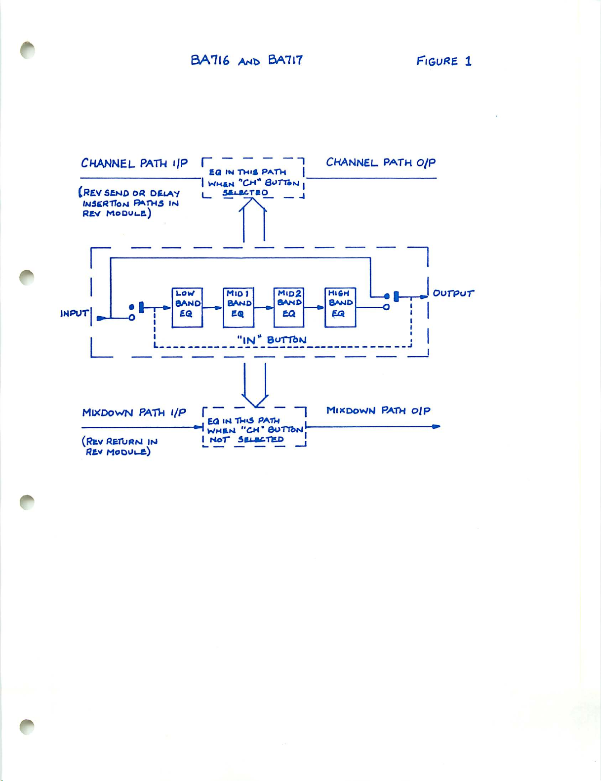
GENERAL - (SEE FIGURE l)
BA716 and 717 are fixed together to form a sandwich assembly mounted near
the centre of the channel or rev modules. A single l6 way flying flatcable
connector connects BA716 to a header on BA7^0.
BA716/717 form a four band fully variable (parametric) equaliser which may
be switched into the Channel or Mixdovn signal paths. The high frequency
and low frequency bands may be switched from a peaking to a shelving characteristic
When used in a Rev module the EQ may be switched into the Rev Send path (or
Delay Insertion path if "INS" button on BA752 is pressed) or the Rev Return path.
USER CONTROLS
Frequency controls : one per band, marked 30Hz - 300Hz ; 200Hz - 2kHz ;
0.8kHz -8kHz ; 1.5kHz - 15kHz. Set band centre frequencies.
Boost/Cut controls : one per band, marked LOW, MID 1, MID 2, HIGH. Set band
boost or cut over range +l8dB.
button : When out , low b and r esponse i s bell s hap ed. W hen in,
lowband response is shelving.
button : Whe n out, h igh band res ponse is bell sha ped. W hen in,
high band response is shelving.
"CH " b utto n : W h en out , E Q i s avail able in the M ixdow n path. W hen in,
EQ is available in the channel path.
"IN" butto n : When o u t , E Q i s b ypasse d . W h en in, EQ is inser t ed i n
the signal path.
NOTE ; As with all parametric equalisers, a certain amount of overlap of
frequency ranges is provided. Careless use can thus result in
ri diculously high gains at certain f requencies whi ch may cau se oscillat ion.
DETAIL
See ET10209 (circuit diagram), EB2036U (channel module block diagram), and
figure 1.
The BA716/717 parametric equaliser may be considered to consist of five
separate sections, each of which is physically split between the two printed
circ u it boards :
a) I n /O u t sw i t c h i n g a n d L E D i n d i c a t o r s w i tc h i n g
b ) L o w b a n d E Q s e c t i o n
c ) M i d 1 b a n d E Q s e c t i o n
d ) M i d 2 b a n d E Q s e c t i o n
All the EQ sections are connected in series.
e ) H i g h b a n d E Q s e c t i o n
INPUT/OUTPUT AND LED SWITCHING
Switch SI ("CH") on BA717 and S2 ("IN") on BA716 enable the equaliser to be
switched into either the Channel or the Mixdown signal paths, and to be either
in circuit or bypassed. One pole of each switch is used to switch LEDS mounted
remotely on BA7^o. IC1 on BA716 is a non-inverting buffer amplifier.
LOW BAND EQ SECTION
BA717 : IC1 amplifiers a, b, and c, form a Two-Integrator loop filter whose
frequency is tuned' by RV1 (30Hz - 300Hz). The filter has a fixed "Q" of 1
and its input is provided by IC2a on BA7l6. Two outputs are taken from the
fil ter to a summing amplifier ICld, one fi lter outp ut and ICl d output th en
going to the shelving switch (SI on BA716).
BA716 : IC2b is used as an inverting summing amplifier to combine the filter
output, selected by SI with the input signal from IC1 buffer. RV1 devices
a voltage which is somewhere between the full input signal (fully clockwise,
full boost) and the full inverted and summed output of IC2b (fully anticlockwise,
full cut). The output of RV1 is amplified by IC2a and is the input for the
filter on BA717. Low band EQ section output is taken from IC2b, and is the inp*
for the Mid 1 EQ section (lC2d etc).
MID 1 BAND EQ SECTION
BA717 : IC2a and d form a modified Two Integrator loop giving only a second
order bandpass output from IC2d. The "Q" of this filter is 2 and centre
frequency set by RV2 (200Hz - 2kHz). Filter input is received from IC2c on
BA7l6, and bandpass output sent to IC2d on BA716.
BA716 : IC2d is used to invert the Mid 1 EQ sections input signal, (from IC2b
the lowpass EQ sections output) and add to it the bandpass filter output received
from IC2d on BA717. RV2 derives a voltage which is somewhere between full input
sign al (full y c l ockwi se, full boos t ) a nd full filte r o u tput m i nus inpu t s ignal
(f ully anticlock wise, f ull cut). The output of RV2 is buffered by IC2c a nd
provides the input for the filter on BA717. Mid 1 band EQ section output is
taken from IC2d and is the input for the Mid 2 band EQ section (lC3a).
The signal at this point has passed through both Low and Mid 1 band EQ
sections in series, each of which operate without interacting.
MID 2 BAND EQ SECTION
The operation of this circuit is identical to that of the Mid 1 band section
described above. It use3 IC2b and c and RV3 (0.8kHz - 8kHz) on BA717, IC3 a
and b and RV3 (boost/cut) on BA716. Input is received frcm IC2c en BA716,
the Mid 1 sections output. Output is sent from IC3b on BA716 to the input of
the high band EQ section. At this point the signal has been operated on
non-interactively by the Low, Mid 1, and Mid 2 band EQ sections.
^ H I G H B A N D E Q SE C T I O N
The operation of this circuit is similar to that of the low band EQ section
described above except that different outputs from the Two Integrator loop
filter on_BA717 (IC3 a - d) are used in order to achieve high pass shelving
characteristics when selected by S2 on BA717. Amplifiers used on BA716 are
IC3c and d. Input is received from IC3b on BA716, the Mid 2 EQ sections
output. Output is sent from IC3c on BA716 back to the "IN" switch S2 on
BA7l6.^ At this point the signal has been operated on by all four EQ sections
in s e r ies, n o n - i n t e r a c t i v e l y.
LEVELS
The BA716/7 circuits are used at a nominal level of -lOdBu.
D.C. SUPPLIES
The BA716/717 EQ assembly runs from +18V regulated power which it receives
from the BA712/713 or BA752/753 assemblies via BA7U0.
TEST POINTS
Test points are provided as follows on BA716.
TPOV OV r efe ren ce
TP 1 Chann el p ath out put fro m EQ
TP2 Mixdown path output from EQ
TP3 EQ input, after p a t h s e l e ction and in/out
TPU Sig nal aft er low- band E Q s ecti on
TP 5 Signa l after M id 1 ba nd EQ section
TP 6 Signa l after M id 2 ba nd EQ section
TP7 S ignal aft er Hig h band E Q sect ion
0A716 an*> BAH7
Figure. 1
Channel path \\p
{RB.V SZ**D OR DfctAV
»W 3_Rl7o*J F KrH3 I H
R E V M o D U u t )
r
IMPUTl
I
MIXDOWN PATH l/P
(Rev RfcTuflM iisi
R f cv M oouuft)
I i
EQ in Thi« PATH
"I whim "CM* Bom* ,
____CT_0_
7\
LOW
BAWD
*iWHW "_>4"eoTT!>i4j
MI01
BAMD
£<*
"IN* BuTTbM
r--^-n
. Ed IM TMvS PATH
I r * © T 3_-_CT_ -»
m»d2
BAND
CHANNEL. PATH 0(P
~i
HifiH
8AKID
Mixdown Path o/p
J output
 Loading...