

Page 1
Power Integrated Processor for Digital Amplifier NTP3000
N
T
P
3
0
0
N
N
T
T
P
P
3
3
0
0
0
0
0
0
0
1 CHIP 2.1 CHANNEL FULL DIGITAL AMPLIFIER
Features
Stereo (30W ⅹ 2)
2.1 channel (15Wⅹ2 + 30W)
Wide Supply Voltage Range
(7V~30V)
Floating Point Operation
18 Programmable Biquad Filters
Speaker Compensation
DC cut, LPF, HPF
Parametric Equalizer
PWM Output for External Subwoofer
3D Surround
7 Band Graphic Equalizer
100 dB Dynamic Range
Adaptive Loudness Compensator
based on Psycho Acoustics
Applications
kHz. It delivers 2x30W in stereo mode or
2x15W + 1x30W in 2.1 channel mode without
heat sink.
Combining use of built-in mixer and biquad
filters can make additional preprocessing like
bass management, loudness control, loud-
speaker response compensation and preset
parametric equalizers possible.
All the functions of NTP3000 are set by I2C
register configuration.
Package
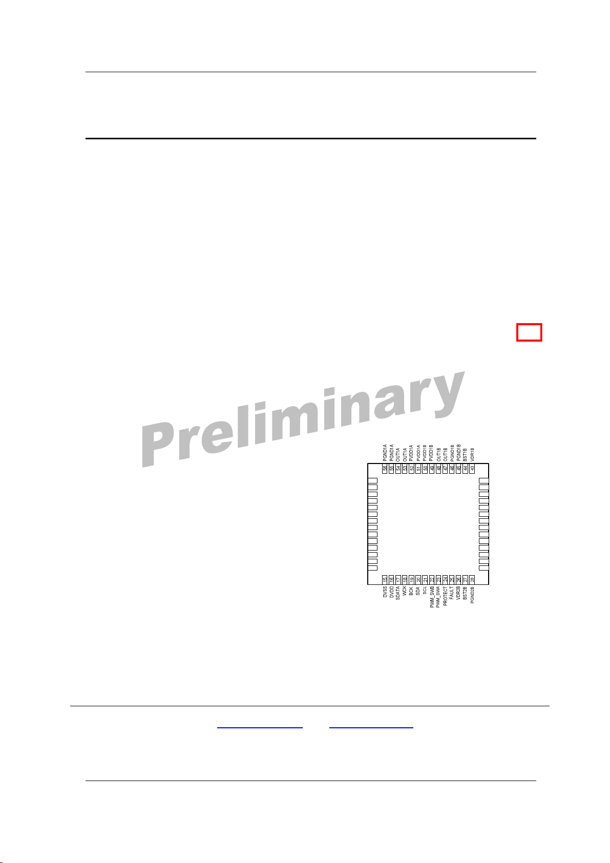
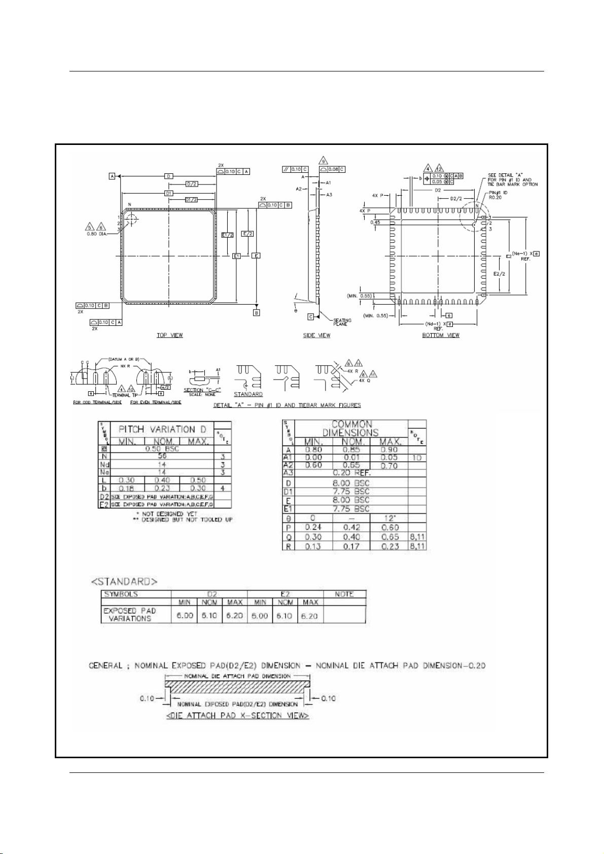
56 pin MLF 8mm by 8mm
Plasma TV, LCD TV
Docking Station
Mini-Component Audio
Description
NTP3000 is a single chip full digital audio
amplifier including power stage for stereo or
2.1 channel amplifier system. NTP3000 is
integrated with versatile digital audio signal
processing functions, high-fidelity fully digital
PWM modulator and two high-power full bridge
MOSFET stages.
NTP3000 receives 2-channel serial audio data
with sampling frequency from 8 kHz to 192
NeoFidelity, Inc. #1009, Ace Twin Tower 2, 212-30, Guro-dong, Guro-gu, Seoul 152-766 Korea, Phone +82-2-66751100, Fax +82-2-6675-1109, Email [email protected], Web www.neofidelity.com
Copyright © NeoFidelity, Inc. 2005 All rights Reserved. June, 2005
Disclaimer
NeoFidelity, Inc. reserves the right to make changes without notice in the product described in this datasheet
BST1A
1
VDR1A
2
/RESET
3
AD
4
VSS_IO
5
CLK_I
6
CLK_O
7
VDD_IO
DGND
PLL
AGND
PLL
LFM
AVDD
PLL
DVDD
PLL
NC
Figure 1 NTP3000 Pin Assignment
NTP3000
8
9
10
11
12
13
14
NC
42
41
VDR2A
BST2A
40
PGND2A
39
PGND2A
38
OUT2A
37
36
OUT2A
PVDD2A
35
34
PVDD2A
PVDD2B
33
PVDD2B
32
OUT2B
31
OUT2B
30
29
PGND2B
Copyright © NeoFidelity, Inc. 2005 1
Preliminary datasheet – NeoFidelity reserves the right to change specifications at any time without prior notice
R0.73-11.2006
Page 2

Power Integrated Processor for Digital Amplifier NTP3000
including circuits, software and ICs, described herein for the purpose of improvement of design and performance.
NeoFidelity, Inc. assumes no responsibilities and liabilities for the use of the product, conveys no license under any
patent or copyright, and makes no warranties that the product is free from patent or copyright infringement, unless
otherwise specified.
Copyright © NeoFidelity, Inc. 2005 2
Preliminary datasheet – NeoFidelity reserves the right to change specifications at any time without prior notice
R0.73-11.2006
Page 3
Power Integrated Processor for Digital Amplifier NTP3000
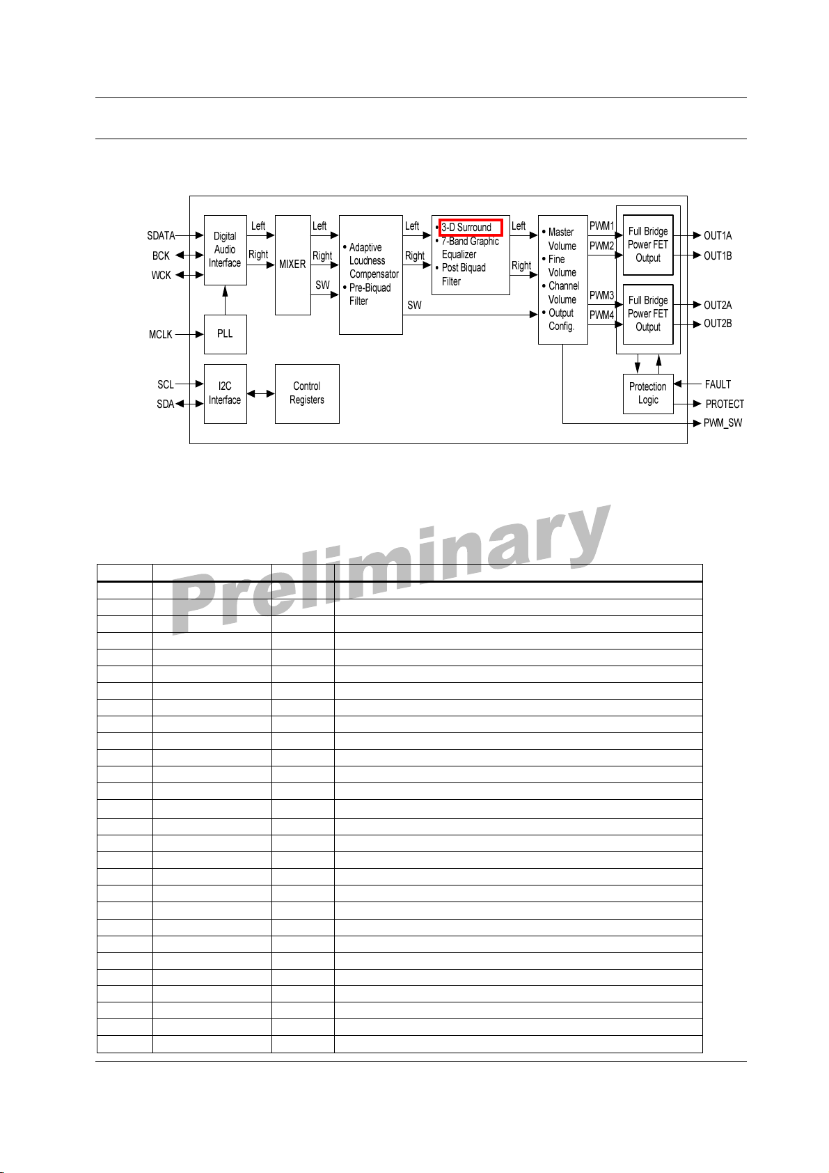
1. BLOCK DIAGRAM
Figure 2 NTP3000 Block Diagram
2. PIN DESCRIPTIONS
PIN NAME TYPE
1
2
3
4
5
6
7
8
9
10
11
12
13
14
15
16
17
18
19
20
21
22
23
24
25
26
27
28, 29
BST1A P
VDR1A P
/RESET I
AD I
VSS_IO -
CLK_I I
CLK_O O
VDD_IO P
DGND
AGND
-
PLL
-
PLL
LFM I
AVDD
DVDD
P
PLL
P
PLL
VSS
DVSS DVDD P
SDATA2) I
WCK2) I/O
BCK2) I/O
SDA2) I/O
SCL2) I
PWM_SWB O
PWM_SWA O
PROTECT O
FAULT I
VDR2B P
BST2B P
PGND2B -
1)
Bootstrap supply, external capacitor to OUT1A is required
Gate drive voltage regulator decoupling pin, capacitor to GND
Active Low to reset NTP3000, Schmitt trigger input
I2C device Address selection
Ground
System master clock input
System master clock output
voltage supply for I/O, 3.3V
Ground
Ground
External loop filter
voltage supply for PLL analog circuit, 1.8V
voltage supply for PLL digital circuit, 1.8V
Ground
-
Ground
voltage supply for core logic, 1.8V
I2S serial data input
I2S word clock
I2S bit clock
I2C data
I2C clock
PWM output for external subwoofer, negative
PWM output for external subwoofer, positive
External power stage on/off control to protect
input from external power stage
Gate drive voltage regulator decoupling pin, capacitor to GND
Bootstrap supply, external capacitor to OUT1A is required
Ground
DESCRIPTION
Copyright © NeoFidelity, Inc. 2005 3
Preliminary datasheet – NeoFidelity reserves the right to change specifications at any time without prior notice
R0.73-11.2006
Page 4

Power Integrated Processor for Digital Amplifier NTP3000
30, 31
32, 33
34, 35
36, 37
38, 39
40
41
42
43
44
45, 46
47, 48
49, 50
51, 52
53, 54
55, 56
OUT2B O
PVDD2B P
PVDD2A P
OUT2A O
PGND2A -
BST2A P
VDR2A P
NC -
VDR1B P
BST1B P
PGND1B -
OUT1B O
PVDD1B P
PVDD1A P
OUT1A O
PGND1A -
Power stage PWM output 2B
Voltage supply for power stage
Voltage supply for power stage
Power stage PWM output 2A
Ground
Bootstrap supply, external capacitor to OUT2A is required
Gate drive voltage regulator decoupling pin, capacitor to GND
No connection
Gate drive voltage regulator decoupling pin, capacitor to GND
Bootstrap supply, external capacitor to OUT2A is required
Ground
Power stage PWM output 1B
Voltage supply for power stage
Voltage supply for power stage
Power stage PWM output 1A
Ground
1) P = Power, I = Input, O = Output, I/O = Input/Output
2) 5V tolerant. Normal I/O pins are 3.3V tolerant if not specified.
3) TEST0 Pin should be connect Ground Pin.
3. CHRACTERISTICS AND SPECIFICATIONS
3.1. Absolute Maximum ratings
Parameter Reference Rating Unit
DVDD voltage DVSS -0.5 ~ 2.5 V
VDD_IO voltage VSS_IO -0.5 ~ 4.4 V
Logic Input voltage VSS_IO -0.5 ~ 5.5 V
Logic output voltage VSS_IO -0.5 ~ 4.4 V
PVDDXX voltage PGNDXX 32 V
OUTXX voltage PGNDXX -0.3 ~ PVDDXX V
BSTXX voltage PGNDXX 40 V
VDRXX voltage PGNDXX 8 V
Storage Temperature Tstg -65 ~ 150
°C
3.2. Recommended Operating Conditions
Parameter Reference Rating Unit
DVDD voltage DVSS 1.62 ~ 1.98 V
VDD_IO voltage VSS_IO 2.97 ~ 3.63 V
PVDDXX voltage PGNDXX 7 ~ 30 V
VDRXX voltage PGNDXX 6 V
Peak output current - 8 A
Ambient Operating
temperature
Tamb -10 ~ 85
3.3. DC Electrical Characteristics
Parameter Symbol Condition Min Typ
Max Unit
Input High Voltage Vih - 2.0 5.5 V
Input Low Voltage Vil - -0.3 0.8 V
Threshold point Vt - 1.45 1.58
Schmitt trig. Low to
High threshold point
Vt+ - 1.44 1.50
Schmitt trig. High to Vt- - 0.89 0.94
1.74 V
1.56 V
0.99 V
Copyright © NeoFidelity, Inc. 2005 4
Preliminary datasheet – NeoFidelity reserves the right to change specifications at any time without prior notice
°C
R0.73-11.2006
Page 5
Power Integrated Processor for Digital Amplifier NTP3000
Low threshold point
Input Leakage Current
Tri-State output
Leakage Current
Il -
Ioz -
±10
±10
Pull-up Resistor Rpu - 39k 65k 116k Ω
Pull-down Resistor Rpd - 40k 56k 108k Ω
Output Low Voltage Vol Iol=2,4,…24mA 0.4 V
Output High Voltage Voh Ioh=2,4,…24mA 2.4 V
Output Low Current Iol Vol=0.4V, 4mA 4.7 8.0 10 mA
Output High Current Ioh Voh=2.4V, 4mA 5.6 11.9
OUT On Resistance R
OUT Current Limit Sourcing and Sinking
Thermal Shutdown
Temperature
PVDDXX=7.5V 0.1 Ω
dson
8 A
160
19 mA
3.4. Performance Specification
Parameter Condition Min Typ Max
Unit
SNR AES17, A-weighting filter 100 dB
THD+N 1W, 1kHz 0.01 %
Output Power Unclip 2x30 W
Output Power Unclip 2x15+30
W
uA
uA
°C
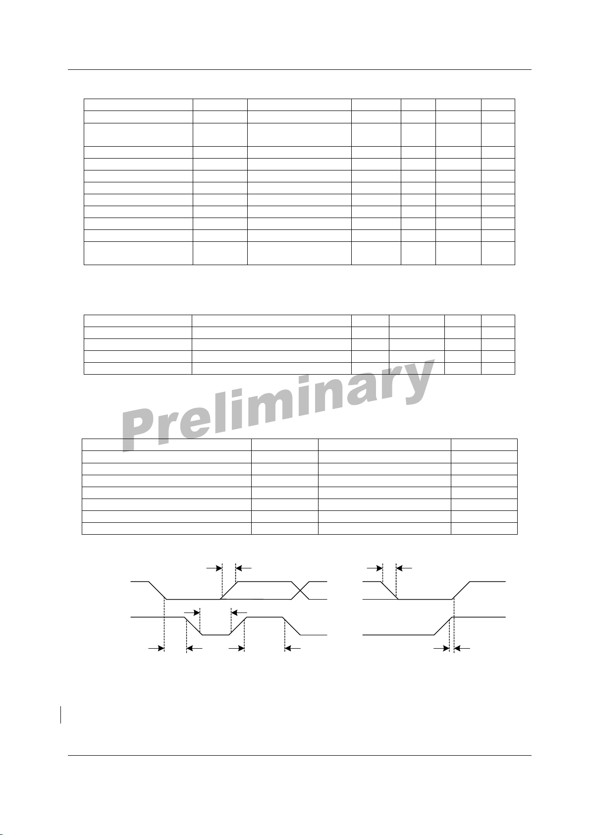
3.5. Switching Characteristics – I2C Control Port
Parameter Symbol Min Max Unit
SCL Clock Frequency f
Hold time for START Condition T
Low period of the SCL clock T
High period of the SCL clock T
Rise time of SDA and SCL signals T
Fall time of SDA and SCL signals T
Setup time for STOP Condition T
-
scl
4000 - ns
hdsta
4700 - ns
low
4000 - ns
high
- 1000 ns
rise
- 300 ns
fall
4000 - ns
susto
400
kHz
SDA
SCL
T
rise
...
T
low
T
fall
...
T
T
hdsta
high
Figure 3 I2C Mode timing
4. I2C Control of NTP3000
All the functions of NTP3000 are controlled by register setting through built-in I2C host interface.
T
susto
Copyright © NeoFidelity, Inc. 2005 5
Preliminary datasheet – NeoFidelity reserves the right to change specifications at any time without prior notice
R0.73-11.2006
Page 6
Power Integrated Processor for Digital Amplifier NTP3000
4.1. Start Condition and Stop Condition
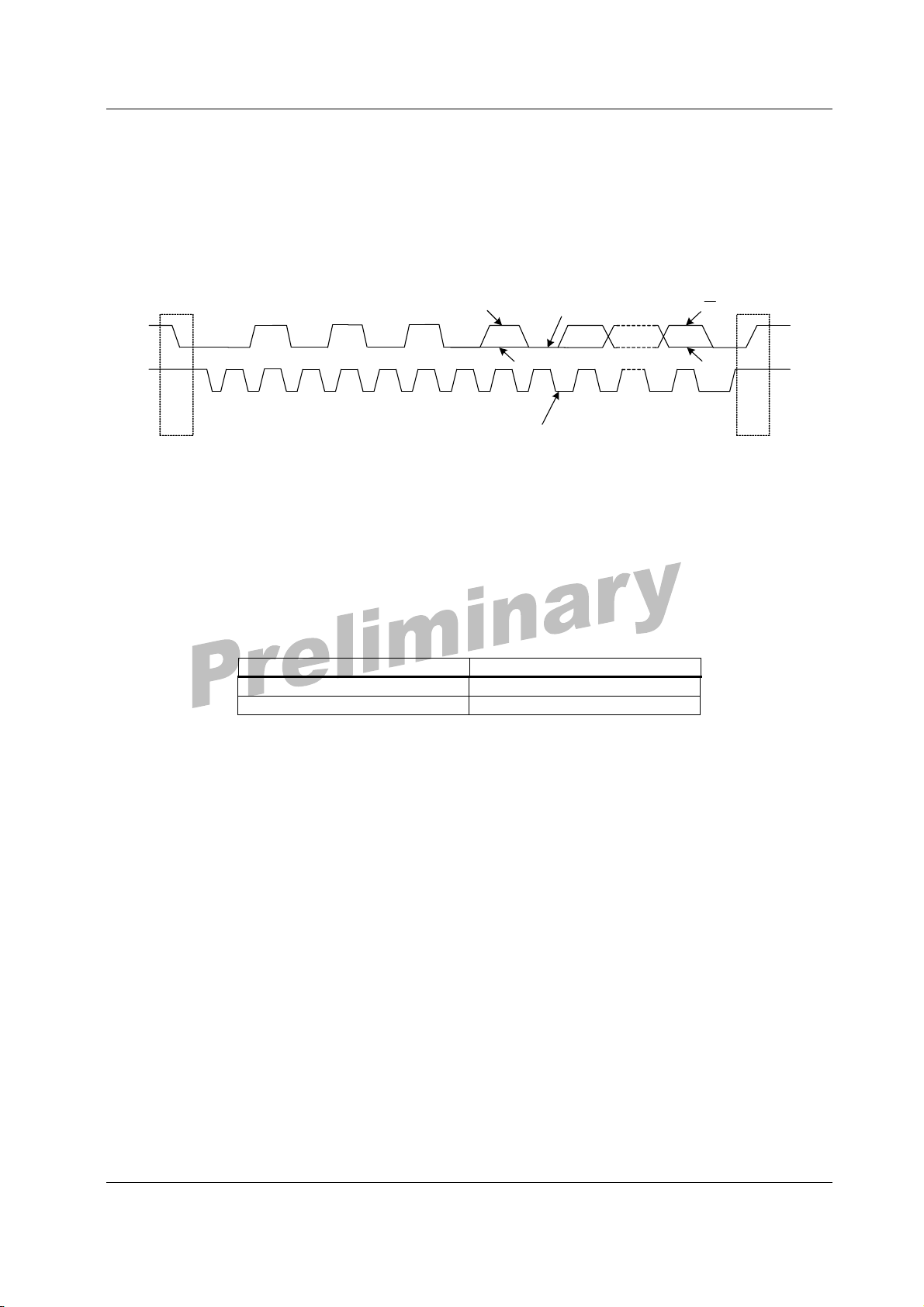
I2C bus of NTP3000 is composed of serial clock line (SCL) and serial data line (SDA). SDA can be
changed only when SCL is in low state with exceptions of start condition or stop condition. START
condition means that master is to start transferring data to slave. To make START condition, transit SDA
state from high to low when SCL is high. STOP condition means that master is to finish transferring data
to slave. To make STOP condition, transit SDA state from low to high when SCL is high.
acklowedgement
signal from NTP-3000
R
A
W
byte complete
MSB LSB
2-8
A
A
9
Sr
or
P
STOP or
repeated START
condition
SDA
SCL
S
or
Sr
START or
repeated START
condition
Slave address
1 000
MSB
1 2 1
1 0
3 4 5 6 7 8 9
1
LSB
Figure 4 START Condition and STOP Condition
4.2. I2C Address
The I2C Address of NTP3000 is composed of 7-bit except for Acknowledge bit with 7th bit depending on
AD pin input (Table 1). If AD is low or pulled down, the Address is 0x54 and if AD is high or pulled up it is
0x56.
AD I2C Address
0 0x54
1 0x56
Table 1 I2C Address
4.3. Write or Read
A bit after 7-bit slave Address means to WRITE (0) or to READ (1).
4.3.1. Writing to NTP3000
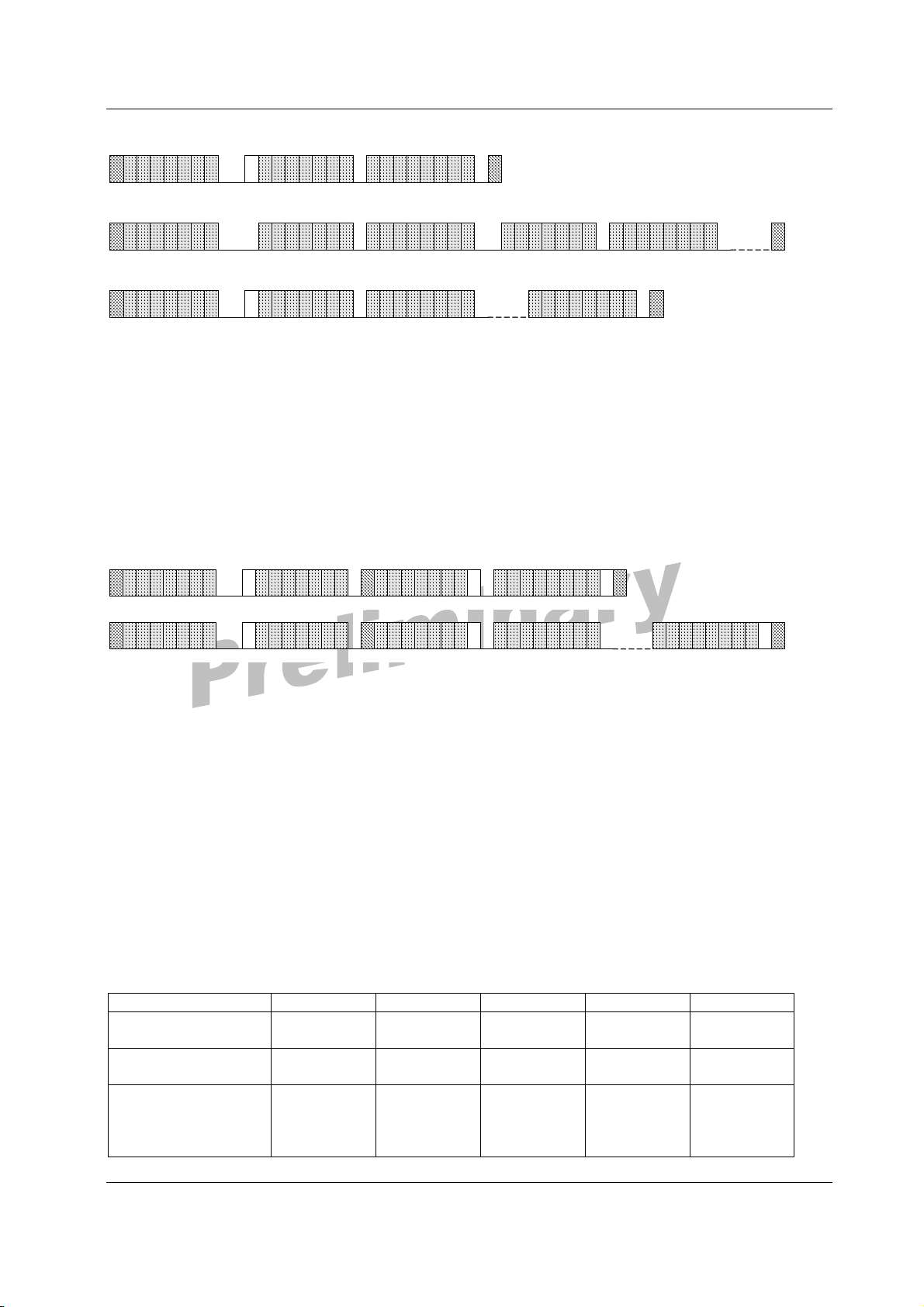
I2C data can be written on NTP3000 by using modified I2C write operation. Figure 5 (a) shows writing 1byte register data procedure. Followed by START condition, master notices the data transfer mode to
NTP3000 by sending slave Address with WRITE operation bit (W). NTP3000 sends acknowledgement
bit (ACK) to master when it receives the slave Address correctly and is ready for response. After
checking the ACK, master sends NTP3000 the sub-Address which means the register Address of
NTP3000. The sub-Address is composed of 7-bit register Address and 1-bit Auto Increment Flag (AIF).
When NTP3000 receives the sub-Address correctly, NTP3000 sends ACK to master. After checking the
ACK, master sends data which means the register value to NTP3000. Master checks ACK and 1-byte
register data writing procedure is finished by initiating the STOP condition.
Notice)
If the sub-Address is floating point coefficient register (0x40 ~ 0x5F), 4-byte register data should be
written.
AIF is used for writing multi-byte to NTP3000. Multi-byte register data writing procedure is shown in
Figure 5 (b), (c).
Copyright © NeoFidelity, Inc. 2005 6
Preliminary datasheet – NeoFidelity reserves the right to change specifications at any time without prior notice
R0.73-11.2006
Page 7
Power Integrated Processor for Digital Amplifier NTP3000
Sub-addressS AIFW A A A PSlave address Data
(a)
Sub-addressS AIFW A A ASlave address Data
(b)
Sub-addressS AIFW A A ASlave address Data AData P
(c)
Sub-addressAIF A AData P
Figure 5 Write Mode Sequence
If AIF=0, sub-Address and data can be repeatedly written after master sends NTP3000 the slave
Address with write operation bit (W) and checks ACK from NTP3000.
If AIF=1, data can be repeatedly written with auto-incremented Address.
4.3.2. Read Operation from NTP3000
Master can read data from NTP3000 by using combined format. Figure 6 shows all the possible
procedures of read operation in NTP3000.
DataSub-addressS AIFW A A ASlave address NAK PSr RSlave address
DataSub-addressS AIFW A A ASlave address Sr RSlave address Data NAK PA
Figure 6 Read Mode Sequence
Followed by START condition, master notices the data transfer mode by sending the slave Address with
write operation bit (W). After checking ACK, master sends NTP3000 the sub-Address with AIF=1 and
checks ACK from NTP3000. To change the operation from writing to reading, master sends the START
condition without STOP condition as repeated start condition (Sr). Followed by Sr, master resends the
slave Address with reading operation bit (R) and checks ACK. Then master can read 1-byte or multibytes from NTP3000. To finish the reading operation, master sends NAK data and STOP condition after
reading the last byte.
4.3.3. Downloading biquad filter coefficients and loudness gain
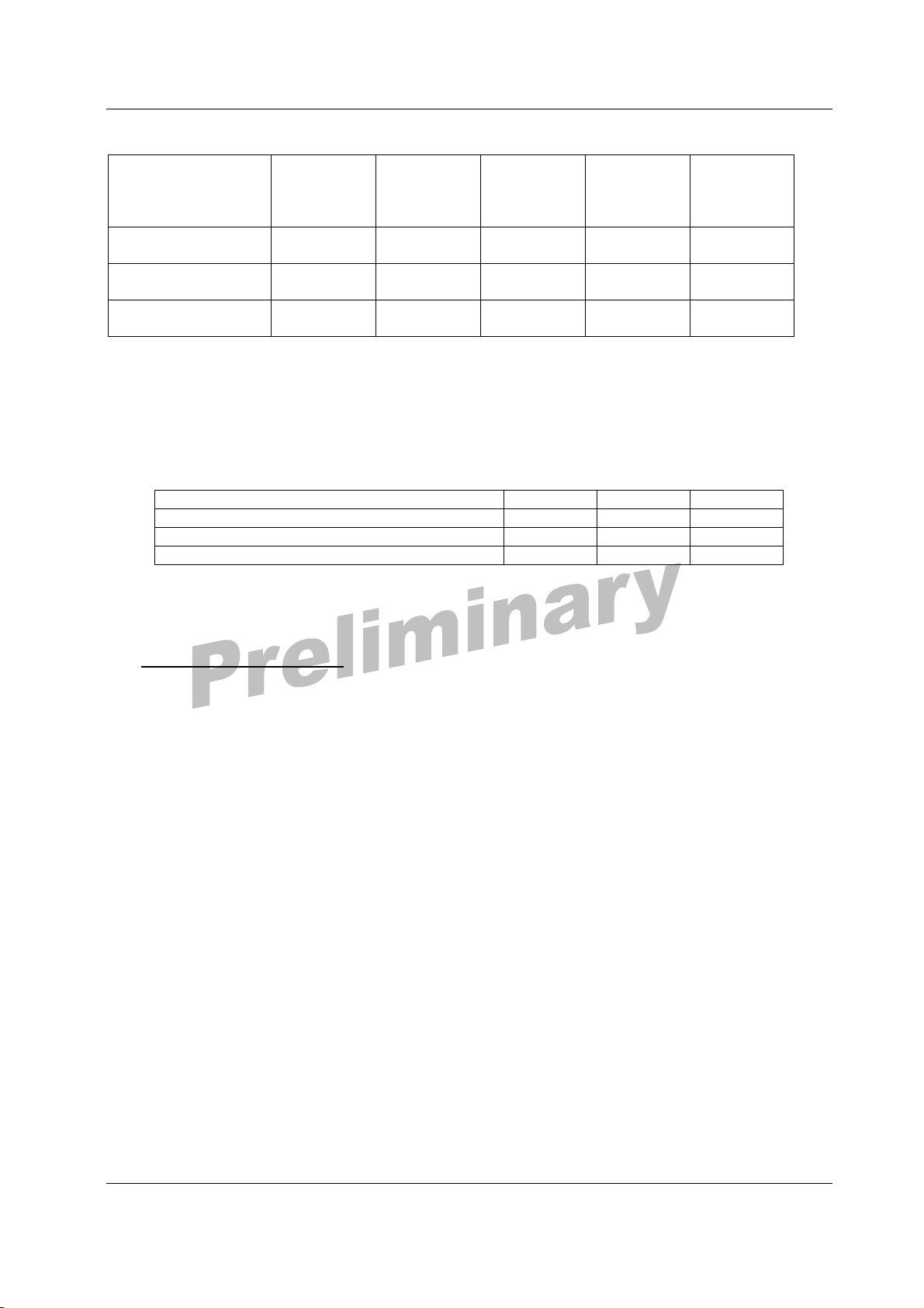
There are 33 programmable biquad filters. To download the filter coefficients of each biquad, the biquad
filter page flag should be set appropriate value.
The number of registers is shown in Table 2.
0x40 ~ 0x44
Post Biquad of CH1
(0x3F = 0x01 case)
Post Biquad of CH2
(0x3F = 0x02 case)
BQ1 BQ2 BQ3 BQ4 BQ5
BQ1 BQ2 BQ3 BQ4 BQ5
0x45 ~ 0x49 0x4A ~ 0x4E 0x4F ~ 0x53 0x54 ~ 0x58
GEQ of CH1
(GEQC flags of 0x06
register = 0b11 &
BQ1 BQ2 BQ3 BQ4 BQ5
0x3F = 0x04 case)
Copyright © NeoFidelity, Inc. 2005 7
Preliminary datasheet – NeoFidelity reserves the right to change specifications at any time without prior notice
R0.73-11.2006
Page 8
Power Integrated Processor for Digital Amplifier NTP3000
GEQ of CH2
(GEQC flags of 0x06
register = 0b11 &
BQ1 BQ2 BQ3 BQ4 BQ5
0x3F = 0x08 case)
3D filter
(0x3F = 0x10 case)
Various1
(0x3F = 0x20 case)
Various2
(0x3F = 0x40 case)
BQ1 of CH1
BQ of ALC
BQ1 of Ch3
Pre-biquad
BQ2 of CH1 BQ1 of CH2 BQ2 of CH2
BQ1 of Ch1
Pre-biquad
BQ2 of Ch3
Pre-biquad
Table 2 Biquad filters
BQ2 of Ch1
Pre-biquad
BQ8 in Post-
Biquad
BQ1 of Ch2
Pre-biquad
BQ9 in Post-
Biquad
X
BQ2 of Ch2
Pre-biquad
X
When the filter coefficients to download are same for, e.g. post biquad of ch1 and ch2 then set the
register 0x3F as 0x3.
There are 8 loudness gains in post-biquad chain. To download loudness gain of each biquad, page flag
register 0x3F should be set as in the case of downloading the filter coefficients.
0x59 0x5A 0x5B
loudness gains of CH1(0x3F = 0x01 case) L11 L12 L13
loudness gains of CH2(0x3F = 0x02 case) L21 L22 L23
loudness gains of CH3(0x3F = 0x80 case) L31 L32 X
Table 3 Loudness gain
5. Clock, Reset & Control
5.1. System Clock
The internal system clock of NTP3000 is generated from external master clock by PLL. NTP3000
supports external master clock frequency from 8.192 MHz to 24.576MHz. For proper operation, PLL
should be set correctly according to master frequency (Table ).
5.2. Reset
When hardware RESET pin is set to low state, NTP3000 is brought into the reset state to bring up the
actions as follow.
1) Each control register resets to the default value.
2) All the internal registers, multipliers, adders, counters, and etc. are cleared to zero.
3) All of the output pins keep low state as long as the RESET is active.
It takes about 7µs after reset pin is remained low for more than 0.1usec to finish the above operations as
shown in Figure 7.
Copyright © NeoFidelity, Inc. 2005 8
Preliminary datasheet – NeoFidelity reserves the right to change specifications at any time without prior notice
R0.73-11.2006
Page 9
Power Integrated Processor for Digital Amplifier NTP3000
>0.1usec
Reset Normal OperationInitialization
5.3. Fault and protect Control
~7us
Figure 7 Reset timing
Figure 8 Protection Logic connection Diagram
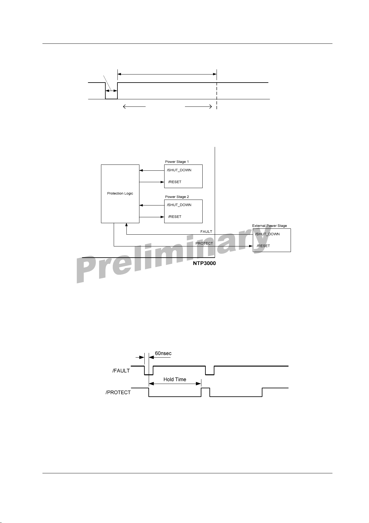
NTP3000 protects internal power stage circuit and external power device with feedback between power
stage and protection logic as shown in Figure 8. When a power stage falls in protection condition, it shuts
down by itself informing protection logic ‘fault’ as shown in Figure 9. As soon as protection logic receives
the information, the output of ‘PROTECT’ becomes low to turn off all the power stages for a ‘Hold Time’
which is configurable. After ‘Hold Time’ has passed, protection logic tries to turn on power stage circuits
again. If power stage circuit still suffers from protection problem, protection logic keeps on turning on and
off until the condition which is configured on control registers.
Figure 9 Fault, Protect pin Timing Diagram
When FAULT signal is changed from high to low, PROTECT signal changes from high to low after
0.06usec.
When this happens, PROTECT signal remains low even the FAULT signal changes to high.
Copyright © NeoFidelity, Inc. 2005 9
Preliminary datasheet – NeoFidelity reserves the right to change specifications at any time without prior notice
R0.73-11.2006
Page 10
Power Integrated Processor for Digital Amplifier NTP3000
PROTECT signal is changed to high by the FAULT signal after Hold Time and at the same time it
increases Auto PROTECT restore counter value by 1.
If the counter value reaches AVRCT (Auto PROTECT Restore Counter Threshold) in Auto PROTECT
restore interval, the PROTECT signal becomes low permanently.
Designers can detect this permanent
low state by reading PPM flag in register Address 0x75 and change the permanent low state to high by
setting Auto PROTECT restore counter value to 0 by using FPMLD flag in register Address 0x1E. Also,
designers can control the PROTECT signal directly by using PWMM flag in register Address 0x1E.
Auto PROTECT restore interval is defined by PHT, AVRCT, IRC flags in register Address 0x1D and the
default value is PHT * AVRCT * IRC = 4 * 5 * 2 = 40msec.
6. Audio Input
6.1. I2S and Serial Audio Interface
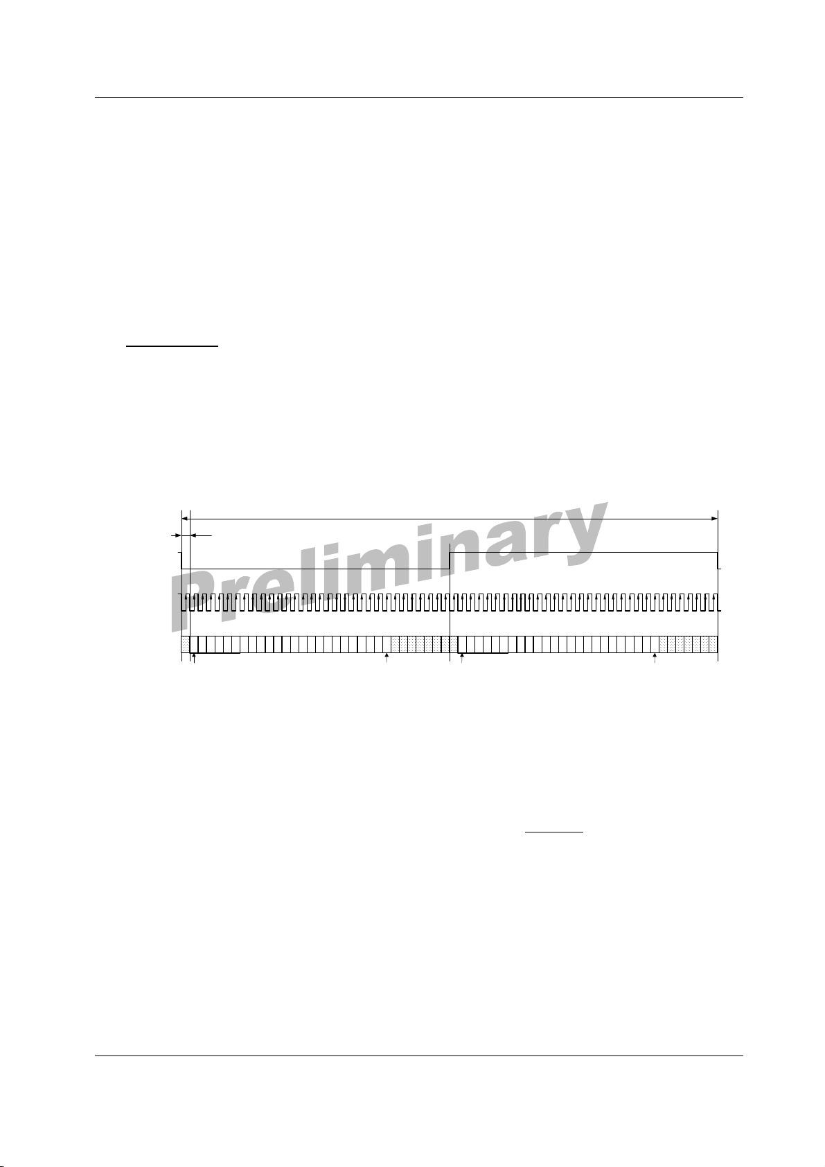
Serial audio port of NTP3000 can be configured as either the master or slave mode, and BCK(bit clock)
and WCK(word clock) are bi-directional pins depending on the clock mode setting. In the master mode,
WCK(fs) and BCK(configurable) are output signals from the NTP3000, and the external DSP receiver
delivers SDATA signal synchronized with them. NTP3000 accepts WCK and BCK signal along with
SDATA coming from external devices in the slave mode. INS flag determines clock mode between
master and slave mode.
1/fs
1/64fs
WCK
(output)
L channel R channel
BCK
(output)
SDATA
(input)
X X X X X X X X X
L23 L22 L21 L20 L19 L18
L17 L16 L15 L14 L13 L12 L11 L10 L9 L8 L7 L6 L5 L4 L3 L2 L1 L0
LSBMSB LSBMSB
L23 L22 L21 L20 L19 L18
X X X X X X XL17 L16 L15 L14 L13 L12 L11 L10 L9 L8 L7 L6 L5 L4 L3 L2 L1 L0
* WCK and BCK are output when master mode, and input when slave mode.
Figure 10 Serial audio interface format
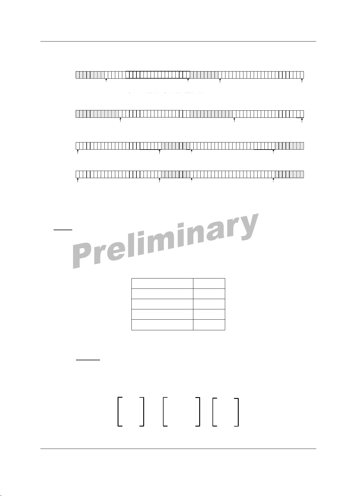
For general serial mode other than I2S, the format of data can be changed by LRJ(Left, Right Justify),
MLF(MSB, LSB First)and BS(Bit Size) flags of register Address 0x01. Figure 11
of general serial audio formats and their register settings.
shows some examples
Copyright © NeoFidelity, Inc. 2005 10
Preliminary datasheet – NeoFidelity reserves the right to change specifications at any time without prior notice
R0.73-11.2006
Page 11
Power Integrated Processor for Digital Amplifier NTP3000
SDATA
(input)
SDATA
(input)
SDATA
(input)
SDATA
(input)
X X X X X X X X X
MSB LSBMSB
X X X X X X X X
LSB
L23 L22 L21 L20 L19 L18
MSB
L17 L16 L15 L14 L13 L12 L11 L10 L9 L8 L7 L6 L5 L4 L3 L2 L1 L0
L17 L16 L15 L14 L13 L12 L11 L10 L9 L8 L7 L6 L5 L4 L3 L2 L1 L0L23 L22 L21 L20 L19 L18 X X X X X X X L17 L16 L15 L14 L13 L12 L11 L10 L9 L8 L7 L6 L5 L4 L3 L2 L1 L0
Register 1 = 00001101 : Right justified, MSB first, 24bit
Register 1 = 00000001 : Right justified, MSB first, 24bit
L17L16L15L14L13L12L11L10L9L8L7L6L5L4L3L2L1L0
LSB
Register 1 = 00000111 : Right justified, LSB first, 20bit
Register 1 = 00001011 : Right justified, LSB first, 20bit
L17L16L15L14L13L12L11L10L9L8L7L6L5L4L3L2L1L0 L23L22L21L20L19L18 X X X X X X X
Register 1 = 00000010 : Left justified, LSB first, 24bit
Register 1 = 00001110 : Left justified, LSB first, 24bit
Register 1 = 00000000 : Left justified, MSB first, 24bit
Register 1 = 00001100 : Left justified, MSB first, 24bit
X X X X X X X X
MSB
X X X X X X X
LSB
L23 L22 L21 L20 L19 L18
LSB
L19L18X X X X
X X X X X X X X
MSB
LSB MSB
X
L23 L22 L21 L20 L19 L18
MSB
L17 L16 L15 L14 L13 L12 L11 L10 L9 L8 L7 L6 L5 L4 L3 L2 L1 L0
LSB
L17L16L15L14L13L12L11L10L9L8L7L6L5L4L3L2L1L0 L23L22L21L20L19L18 X
X X X X X X X
LSB
L17L16L15L14L13L12L11L10L9L8L7L6L5L4L3L2L1L0 L19L18X X X X
MSB
X
Figure 11 General serial audio data formats
7. Mixer
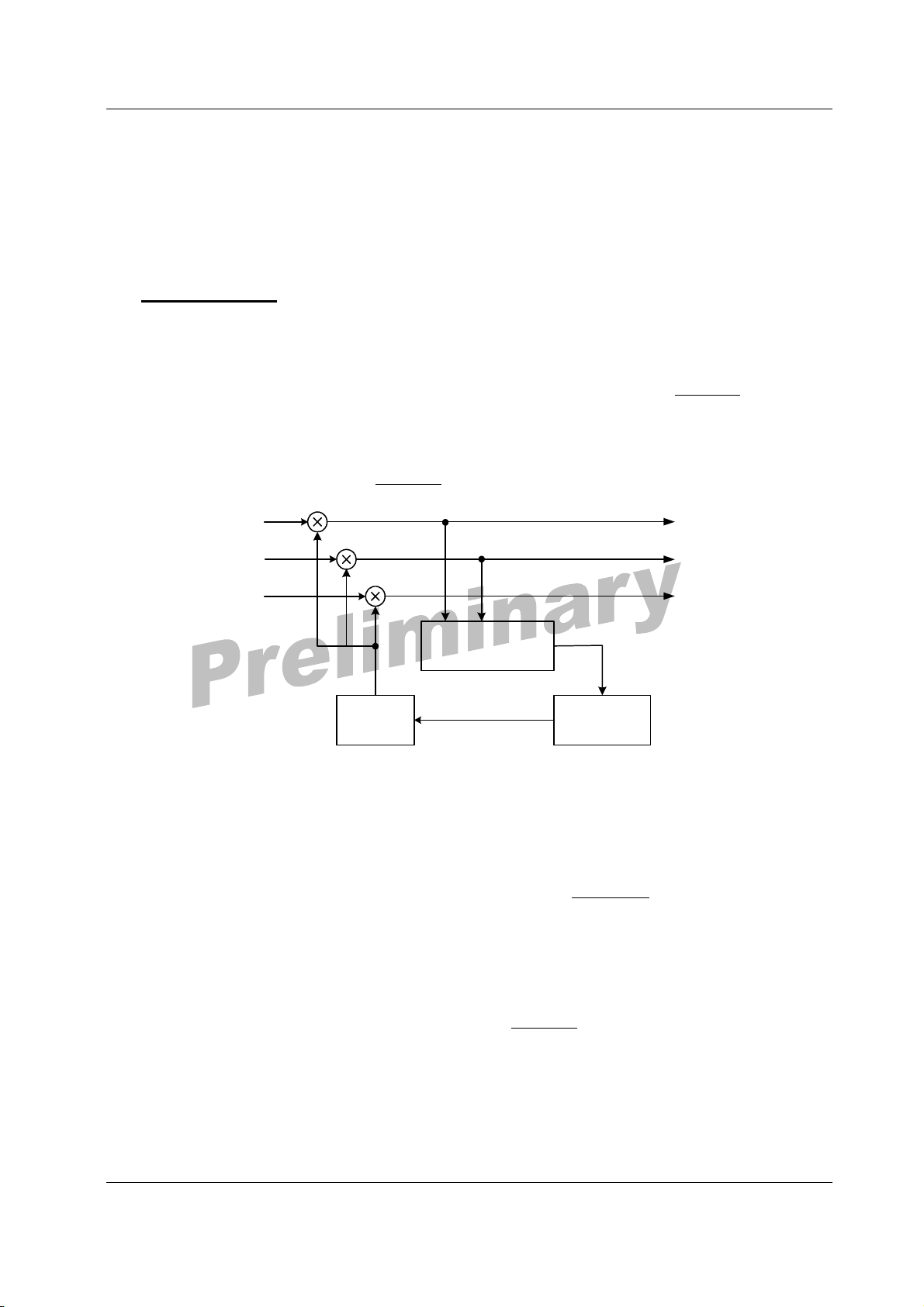
Channel mixer can be used in lots of application needs like bass management, subwoofer signal
generation, pseudo stereo, etc. Mixer cross-connects two input channels to three output channels. Mixer
can control both gain and polarity of each channel input. Step size of mixer gain change is also variable
according to the gain level as shown below.
Table 4 Variable step mixing gain
Volume Range(dB) Step(dB)
+18 ~ + 6 1
+5.5 ~ -5.5 0.5
-6 ~ -32 1
< -32
-∞
In total, 6 mixing gain coefficients denoted as M00, M01, M10,…, M21 are defined as shown in the
equation below. Each Mxx stores volume value in dB scale, and the number values versus gain in dB are
shown in the appendix
. There are some places in the mixing matrix that are considered as trivial
connections and thus predefined as -∞ dB.
[Output Channels] = [Mixer Matrix] x [Input Channels]
CH1 OUT
CH2 OUT
CH3 OUT
=
M00
M10
M20
M01
M11
M21
.
CH1 IN
CH2 IN
Figure 12 Mixer matrix
Copyright © NeoFidelity, Inc. 2005 11
Preliminary datasheet – NeoFidelity reserves the right to change specifications at any time without prior notice
R0.73-11.2006
Page 12
Power Integrated Processor for Digital Amplifier NTP3000
In order to load mixer coefficients into internal memory, send the coefficient value itself to the register
Address 0x37 ~ 0x3C. Total 6 registers are preserved and matched to M00, M01, M10, M11, M20, M21,
sequentially.
8. Pre-processing
8.1. Adaptive Loudness Compensation
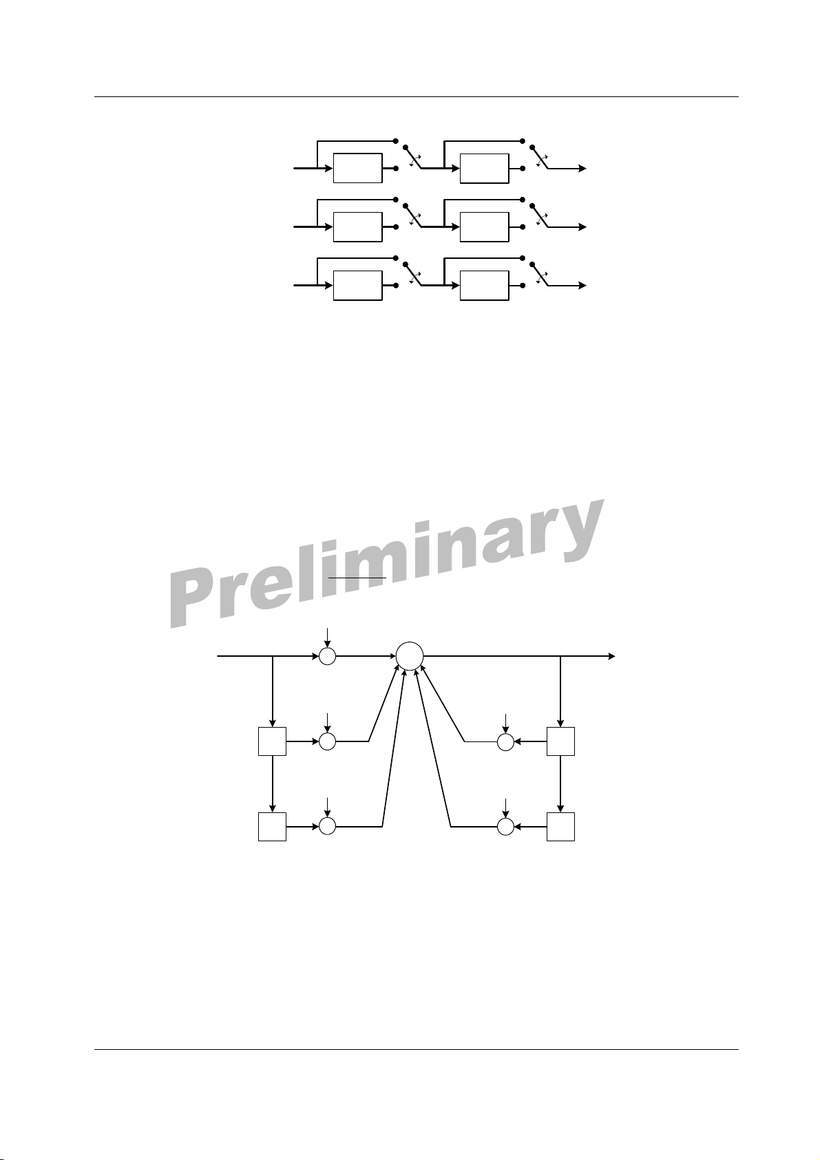
NTP3000 supports Adaptive Loudness Control (ALC) function. This function makes the identical input
signal level without sacrificing the dynamic range.
The difference with the Dynamic Range Compression (DRC) function described in Section 9
is as
follows; DRC sustains the signal level when volume is operating but ALC sustains the signal level when
volume is not operating – that means ALC sustains the signal level of the original input source.
Also, DRC operation is performed by peak detection scheme and ALC is performed by energy detection
scheme.
ALC structure of NTP3000 is shown in Figure 13
.
Ch 1
Ch 2
Ch 3
Psycho-Acoustic
Compensation
Gain
Controller
Level
Detector
Figure 13 Adaptive Loudness Compensation Diagram
ALC can be useful to compensate the signal level difference of different channels and different programs
in same channel in TV related product applications. There is a biquad filters in the Psycho-Acoustic
Compensation block. To download the filter coefficients of this biquad, the page flag register 0x3F should
be set to 0x20 and the five 32 bit coefficients should be downloaded to 0x40 ~ 0x44.
See the system register Addresses 0x07~09, 0x3F, 0x40~44 in the Appendix 1
. The downloading
method will be described in detail on the separate application note.
8.2. Pre Biquad Filter Chain
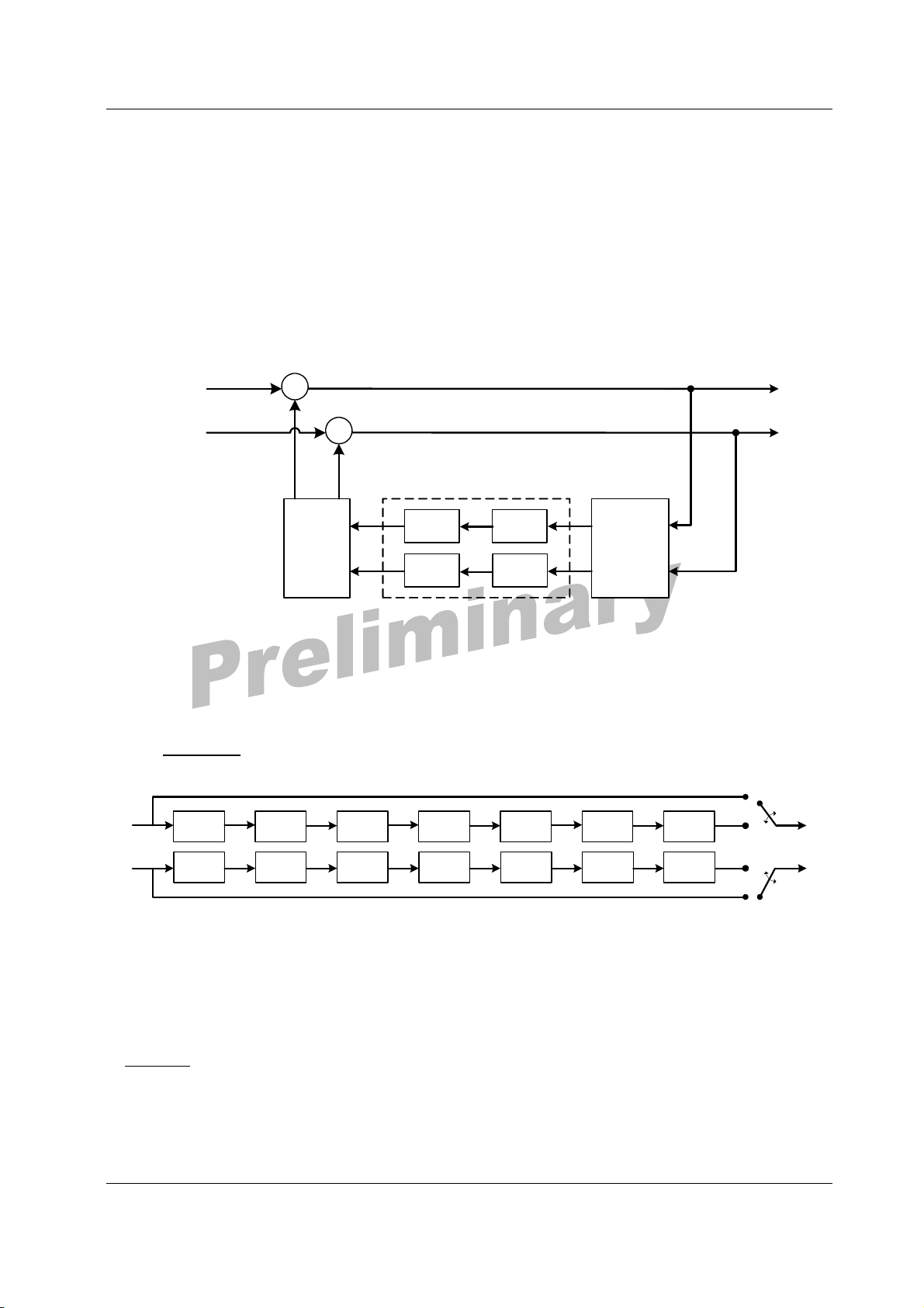
NTP3000 has two kinds of biquad filter chains. One is Pre biquad filter chain and the other is Post
Biquad filter chain for bass management, loudness control, loud-speaker EQ, etc.
The former is called pre-biquad filter chain and two 2nd order floating point biquad filters are connected
serially to all the three channels. The structure is shown in Figure 14
.
Copyright © NeoFidelity, Inc. 2005 12
Preliminary datasheet – NeoFidelity reserves the right to change specifications at any time without prior notice
R0.73-11.2006
Page 13
Power Integrated Processor for Digital Amplifier NTP3000
CH 1
CH 2
CH 3
BQ1
BQ1
BQ1
0
1
0
1
0
1
BQ2
BQ2
BQ2
0
1
0
1
0
1
Figure 14 Biquad Filter Structure
Filter coefficients are 32-bit floating point numbers and can be downloaded thru I2C interface. To
download the pre-biquad filter coefficients to internal memory of NTP3000, designer should change the
Various 1 for Channel 1&2 and Various 2 for Channel 3 flags of register Address 0x3F to ‘enable
coefficient write’ status. And then write the actual coefficient values to ten register Addresses, from 0x40
to 0x53.
When Various 1 Flag of Address 0x3F is set to 1, Address 0x40~44 designates coefficients of 1st prebiquad filter chain of channel 1 and indicates b0, b1, b2, a1, a2 respectively. Address 0x45~49
designates the coefficients of 2nd chain of channel 1, 0x4A~4E for 1st chain of channel 2, and 0x4F~53
for 2nd chain of channel 2.
When Various 2 Flag of Address 0x3F is set to 1, Address 0x40~44 designates coefficients of 1st prebiquad filter chain of channel 3 and Address 0x45~49 designates the coefficients of 2nd chain of channel
3,
The biquad filter structure is shown in Figure 15
.
b
0
x
b
1
-1
Z
-1
Z
x
b
2
x
+
a
1
-1
x
a
2
x
Z
-1
Z
Figure 15 Biquad Filter Structure
8.3. 3D Surround
3D surround expands the sound field of two channel stereo to the extent that is wider than the actual
speaker spacing. Because this feature is acoustically valid for two channel signal, no other channels
except channel 1/2 have this internal block.
Copyright © NeoFidelity, Inc. 2005 13
Preliminary datasheet – NeoFidelity reserves the right to change specifications at any time without prior notice
R0.73-11.2006
Page 14
Power Integrated Processor for Digital Amplifier NTP3000
NTP3000 realizes the 3D effect by combining delay and band-pass filter. At first, define the size of delay
by using register Address 0x60. Possible maximum delay is 40 samples delay and this is about 0.4msec
based on 96kHz signal input.
And then download the band-pass filter coefficients to internal memory of NTP3000(same with the
biquad filter coefficient download procedure). The BPF is two 2nd order IIR filter. Each channel can have
different BPF. Change the 3D flag status of register Address 0x3F to ‘enable coefficient write’ status and
write the actual coefficient values to twenty register Addresses 0x40~ 0x53. Also, internal 2x2 mixer
helps ease of design. For using 3D mixer, download the gain values to four register Addresses
0x5C~0x5F.
Ch 1
Ch 2
+
2x2
+
BQ1BQ2
Delay
Mixer
Figure 16 3D surround Diagram
8.4. Configurable Graphic Equalizer
NTP3000 provides 7 or 5 band graphic equalizer and tone control to 1/2 channel. EQ on/off can be
selected by GEQC flag of register Address 0x06.
The gains for each band can be controlled by writing the gain values (refer Graphic equalizer band gain
table in Appendix 2
In tone control mode the BQ1 ~ BQ5 can be used as programmable biquad filters.
BQ1 BQ2
BQ1 BQ2
) to register Addresses 0x32~36 respectively.
BQ3 BQ4
BQ3 BQ4
Figure 17 GEQ filter structure
BQ1BQ2
0
BQ5
BQ5
BQ6
BQ6
BQ7
BQ7
1
1
0
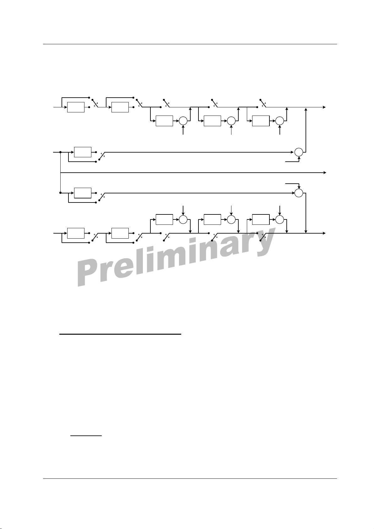
8.5. Post Biquad Filter Chain
The post biquad filter chains of NTP3000 can be used in various purposes - bass management, loudness
control, parametric EQ, loud-speaker EQ, etc.Independent filter design for 1, 2 channels are possible and
five 2nd order floating point parametric filters are linked serially. Especially for loudness control, as shown
in Figure 18
Filter coefficients are 32-bit floating point numbers and can be downloaded thru I2C interface. To
download post biquad filter coefficients to NTP3000, select download channel by using CH flag in
register Address 0x3F first. And then write actual coefficient values to 25 register Addresses, from 0x40
to 0x58.
Copyright © NeoFidelity, Inc. 2005 14
Preliminary datasheet – NeoFidelity reserves the right to change specifications at any time without prior notice
, last 3 filters are different from first 2 filters.
R0.73-11.2006
Page 15
Power Integrated Processor for Digital Amplifier NTP3000
Address 0x40~44 designates 1st chain coefficients and means b0, b1, b2, a1, a2 in sequence. Address
0x45~49designates 2nd chain, and so on.The enable/disable operation of these biquads can be made by
using BQF flag in register Addresses 0x3D~3E.
BQ1
0
1
BQ2
0
1
1
0
1
0
1
0
BQ8
BQ9
BQ1
BQ3 x
L
11
1
0
1
0
L
21
BQ3 x
1
BQ2
0
1
0
0
1
BQ4 x
L
BQ4 x
0
1
BQ5 x
12
L
13
x
L
31
L
32
x
L
22
L
23
BQ5 x
0
1
Figure 18 Post Biquad Filter Chain
For the enhancement of 3D effect or redirection of Bass signal back into Main channel, Ch3 fire back
structure is integrated like Figure 14.
8.6. Loudness
NTP3000 provides loudness control function using post biquad filter chains. Loudness control means the
compensation of frequency characteristics in low volume level to fit the human ear condition.
9. Volume & Dynamic Range Control
Master and channel volumes are independently controlled and softly changed. The system register
Address 0x2E is the master volume control that affects all 3 channels simultaneously and the Address
0x2F~31 correspond to the channel volume control register from 1 to 3 respectively.
The possible maximum of signal boost is +48.4375dB using master volume fine control because the
master volume varies the gain of input signal independent from a channel volume, and a clipping might
occur preventing overflow error if the input signal magnitude is large enough when the combined volume
setting is higher than 0dB at the same time.
9.1. Master Volume Control
By setting volume control registers, master volume is controlled between infinity and +24dB with
changing step size as follows. For details on the master volume setting, see the register value table
shown in Appendix 2
.
Copyright © NeoFidelity, Inc. 2005 15
Preliminary datasheet – NeoFidelity reserves the right to change specifications at any time without prior notice
R0.73-11.2006
Page 16

Power Integrated Processor for Digital Amplifier NTP3000
Table 5 Level dependent master volume steps
Step Range
0.5 dB +24 ~ -100 dB
10dB -100 ~ -150 dB
9.2. Channel Volume Control
By setting volume control registers, channel volumes are independently controlled between infinity and
+24dB with changing step size as described below, and in the Appendix 2
, exact values for channel
volume setting are described.
Table 6 Level dependent channel volume steps
Step Range
0.5 dB +24 ~ -100 dB
10dB -100 ~ -150 dB
9.3. Master Volume Fine Control
Fine control for master volume is possible (+0.0625dB step upto maximum +0.4375dB boost). Refer the
system register Address 0x2D in the Appendix 1
.
9.4. Master Volume Override
By setting the master volume override flag on each channel, the master volume is not applied to the
configured channels. See the system register Address 0x0A in the Appendix 1
.
9.5. Mute
NTP3000 enters mute state by setting soft mute flag of register Address 0x20. Soft mute is implemented
so that the volume gradually increases or decreases when mute is turned off or on respectively.
Also the soft mute speed and soft volume change speed rates are programmable. Designers can
minimize the pop noise by controlling the soft mute speed and volume change intervals. Refer SMC, SVI
flag of register Address 0x06.
9.6. Auto-mute
The chip mutes audio signal if the input signal level is below auto mute threshold during auto mute
inspection interval that are programmable by register setting. Also, the behavior when auto mute has
been entered is changeable between 50:50 switching on or off.
Auto-mute is supported for internal channels 1~3 after 2x3 mixer block. Refer register Addresses 0x04
and 0x05.
9.7. Dynamic Range Control
Dynamic range compression can be turned on or off with programmable compression threshold and
attack/release rates. The threshold parameters of DRC can be controlled separately for channel 1/2 and
channel 3. For detailed setting, please refer system register Addresses 0x0E~10.
Copyright © NeoFidelity, Inc. 2005 16
Preliminary datasheet – NeoFidelity reserves the right to change specifications at any time without prior notice
R0.73-11.2006
Page 17
Power Integrated Processor for Digital Amplifier NTP3000
10. Output Interface
10.1. Output mode configuration
The output mode of NTP3000 is 2.0 stereo reproduction mode and 2.1 reproduction mode. For this
configuration register 0x0B~0x0D should be set to appropriate values.
10.2. AM Interference relief mode
The NTP3000 has AM interference reduction mode. In this mode SNR performance of NTP3000 can be
degrade to 90 dB and the PWM switching frequency is spread to 384kHz ~ 768kHz.
10.3. PWM Output Mapper
Any internal channel from one through three that procedures PWM output can be assigned to any PWM
output hardware port(or pin) by mapping output port register. This feature is very helpful for the hardware
designer because it can relieve difficulties in the power stage signal routing and channel assignment if
the output channel order is fixed. See the system register address 0x0B~0x0D in the Appendix 1
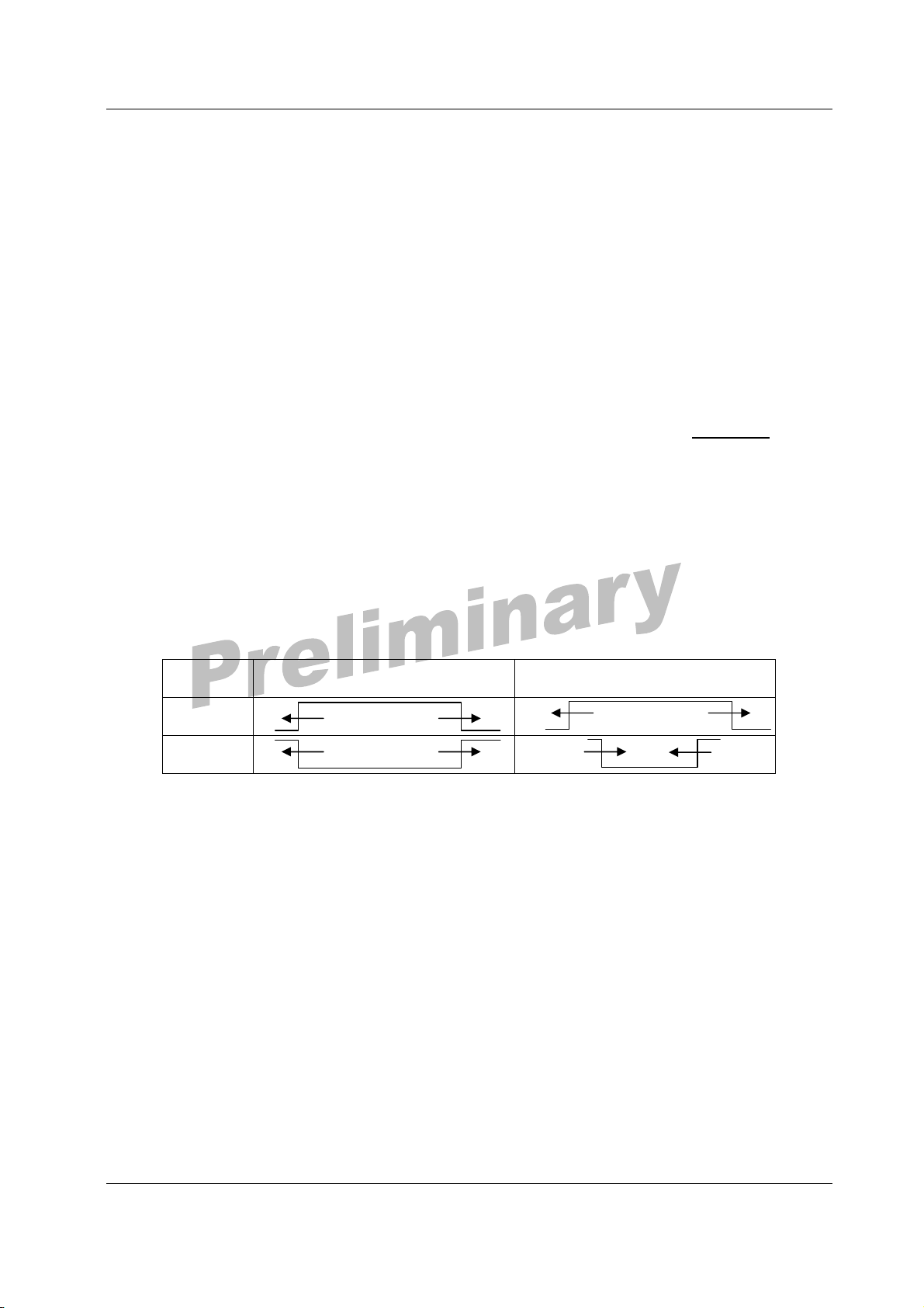
10.4. Switching Output Mode
There are three selectable switching signal output modes called AD and BD mode in NTP3000.
The difference among these output modes is the relative signal pattern relationship between PWM
OUTxA and PWM OUTxB for the channel x.
The selection of output mode is dependent upon the topology of the output stage within NTP3000, and
the design target and policy. AD mode can be applied to both half bridge and full bridge output stage.
BD mode can be used for full bridge output stage only. MD flag of register address 0x03 set the output
mode, then set the design stage.
Table 7 PWM Output Mode
.
Mode
Output A
Output B
AD BD
AD asynchronous pair means the normal AD mode PWM output. In other words, A output and B output
of each PWM output pair are mutually complement. In the case of AD asynchronous pair, A output and B
output is perfectly identical, not in complement relation. That is useful in some special case including
single-ended power stage design.
Copyright © NeoFidelity, Inc. 2005 17
Preliminary datasheet – NeoFidelity reserves the right to change specifications at any time without prior notice
R0.73-11.2006
Page 18
Power Integrated Processor for Digital Amplifier NTP3000
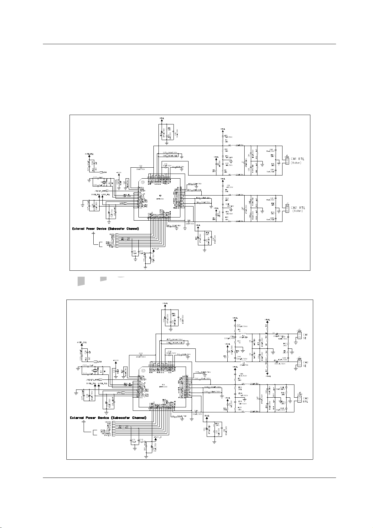
11. Typical Application Schematics
11.1. Schematics for 2 Full bridge reproduction mode
11.2. Schematics for 2 Half bridge and 1 Full bridge reproduction mode
Copyright © NeoFidelity, Inc. 2005 18
Preliminary datasheet – NeoFidelity reserves the right to change specifications at any time without prior notice
R0.73-11.2006
Page 19
Power Integrated Processor for Digital Amplifier NTP3000
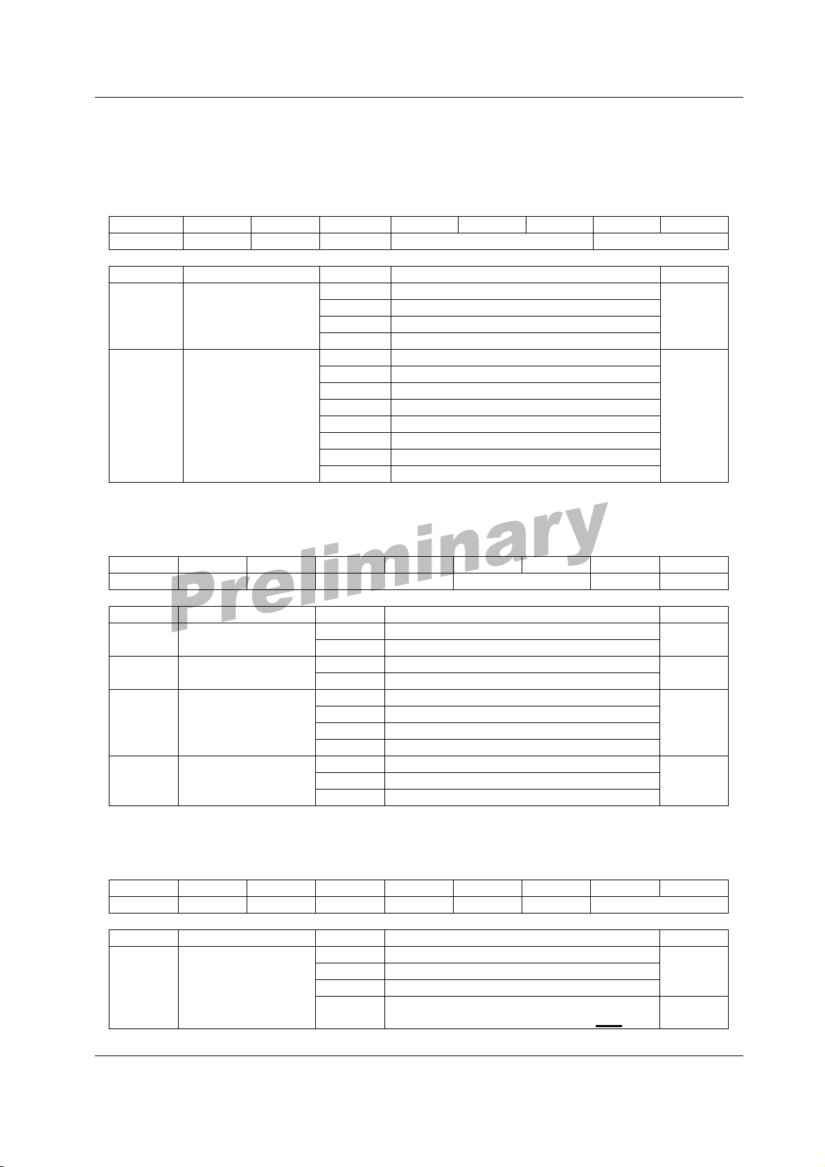
A1. Configuration Register Summary
Table 8 Address 0x00: Input Format
Bit 7 6 5 4 3 2 1 0
Name X X X FSM INS
Name Description Value Meaning Ref.
INS Input format
Sampling
FSM
Frequency
in Master mode IIS
00
01 I2S, master mode
10 General serial audio, slave mode
11 General serial audio, master mode
000
001 8 kHz
010 16 kHz
011 32 kHz
100 12 kHz
101 24 kHz
110 96 kHz
111 192 kHz
I2S, slave mode
48 kHz
Table 9 Address 0x01: General Serial Audio Format
Bit 7 6 5 4 3 2 1 0
Name X X BCKS BS MLF LRJ
Name Description Value Meaning Ref.
LRJ Serial data justify
MLF Serial bit order
BS Serial bit size
0
1 Right justify
0
1 LSB first
00
01 20 bit
10 18 bit
Left justify
MSB first
24 bit
11 16 bit
BCKS Bit clock size select
00
01 48 BCK/WCK
64 BCK/WCK
10 32 BCK/WCK
Table 10 Address 0x02: Master clock frequency control
Bit 7 6 5 4 3 2 1 0
Name X X X X X X MCF
Name Description Value Meaning Ref.
MCF
Master Clock
Frequency
00
01 24.576 MHz
10 18.432 MHz
11 User defined frequency. Required to set
12.288 MHz
address 0x7D and address 0x7E first
.
See
Table
Copyright © NeoFidelity, Inc. 2005 19
Preliminary datasheet – NeoFidelity reserves the right to change specifications at any time without prior notice
R0.73-11.2006
Page 20
Power Integrated Processor for Digital Amplifier NTP3000
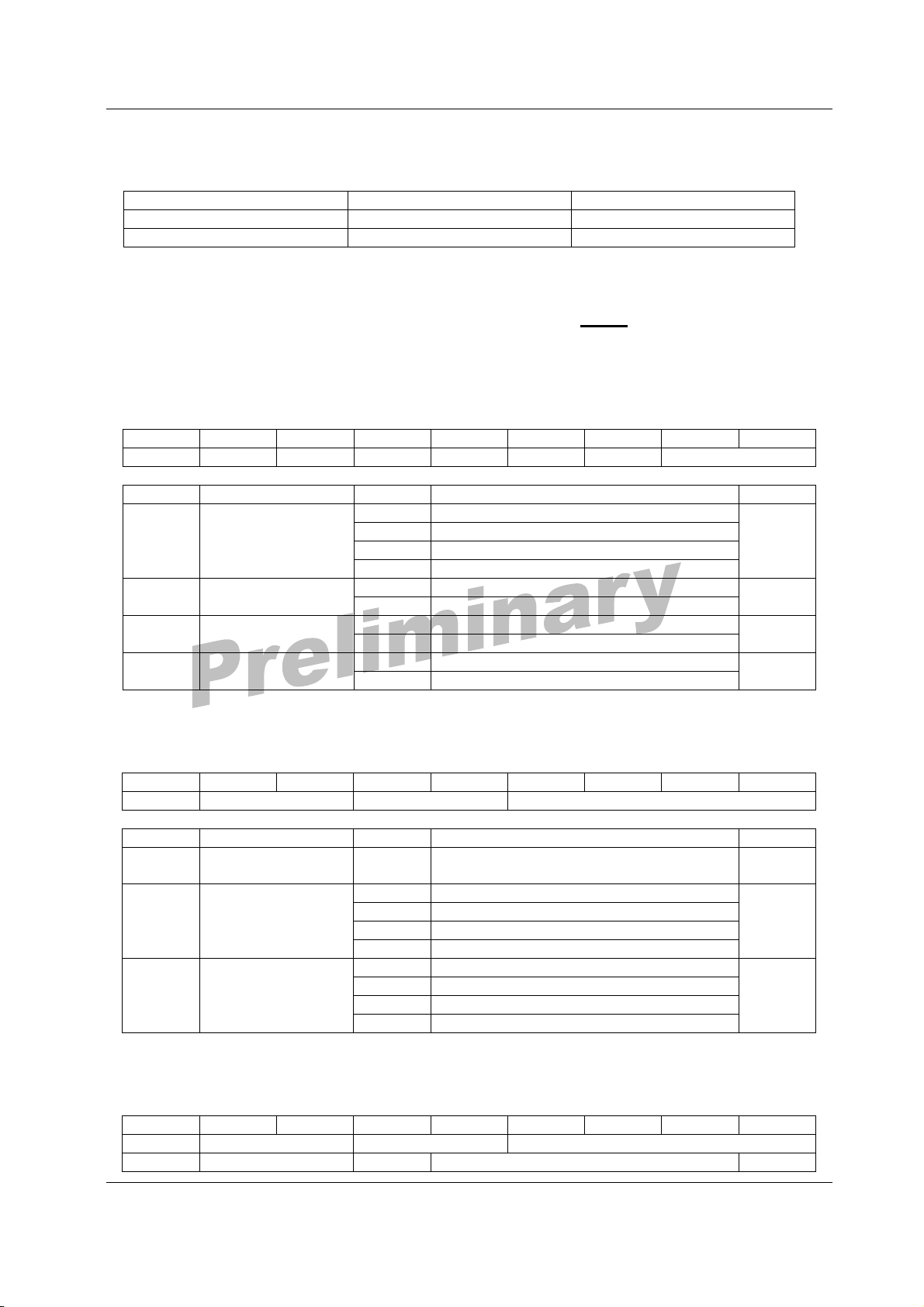
Table 11 User defined master clock frequency
Master Clock Frequency Address 0x7D Address 0x7E
8.192MHz 0xC0 0x16
16.384MHz 0xE1 0x16
Caution 1) Register values different from those on the table are forbidden.
Caution 2) Writing values on Address 0x7D and 0x7E with MCF user defined frequency mode can make
system unstable. Address 0x7D and 0x7E must be configured before
MCF is set as user defined
frequency.
Table 12 Address 0x03: Miscellaneous Control
Bit 7 6 5 4 3 2 1 0
Name X X BHL AHL X POL MD
Name Description Value Meaning Ref.
MD PWM output mode
00
01 AD mode with synchronous signal pair
10 BD mode
AD mode with asynchronous signal pair
11 AM Interference mode
POL
AHL
BHL
Ch. 3 polarity
Control
A-out state
When switching off
B-out state
when switching off
0
1 Inverse polarity
0
1 High
0
1 High
Normal
Low
Low
Table 13 Address 0x04: Front Auto-mute control for channel 1, 2
Bit 7 6 5 4 3 2 1 0
Name EAMC II AT
Name Description Value Meaning Ref.
AT
II
Auto-mute
detection threshold
Auto-mute
response time
00~0F
00
See Auto-mute detection threshold tables
5 msec
01 50 msec
10 500 sec
11 2 sec
EAMC
Effect of Auto-mute
condition
00
01 Channel SoftMute
10 50:50 switching if auto-mute
Auto mute disable(No-Effect)
11 Stop switching if auto-mute
Table 14 Address 0x05: Front Auto-mute control for channel 3
Bit 7 6 5 4 3 2 1 0
Name EAMC II AT
Name Description Value Meaning Ref.
Copyright © NeoFidelity, Inc. 2005 20
Preliminary datasheet – NeoFidelity reserves the right to change specifications at any time without prior notice
R0.73-11.2006
Page 21
Power Integrated Processor for Digital Amplifier NTP3000
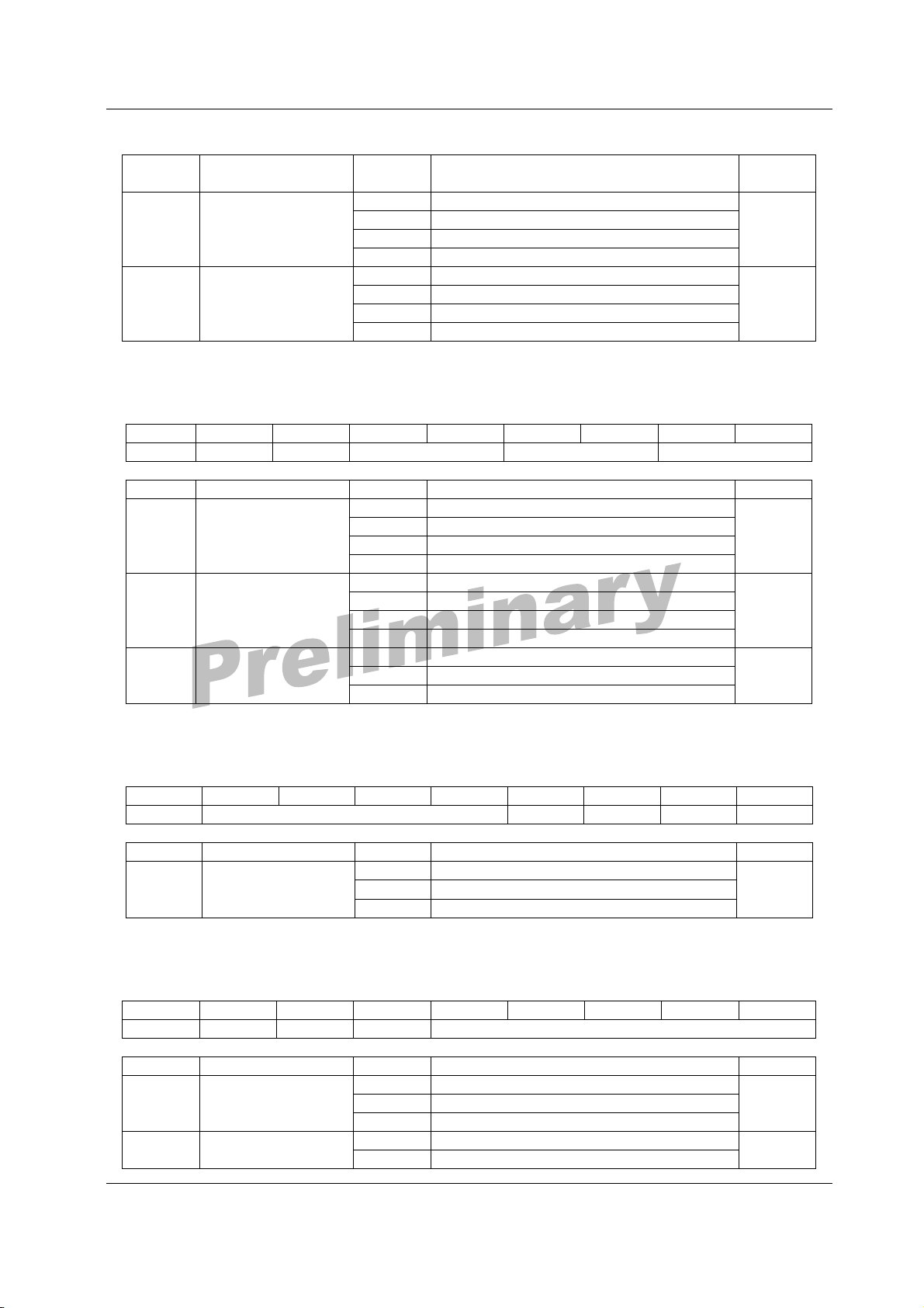
AT
II
Auto-mute
detection threshold
Auto-mute
response time
00~0F
00
See Auto-mute detection threshold tables
5 msec
01 50 msec
10 500 sec
11 2 sec
EAMC
Effect of Auto-mute
condition
00
01 Channel SoftMute
10 50:50 switching if auto-mute
Auto mute disable(No-Effect)
11 Stop switching if auto-mute
Table 15 Address 0x06 : Various configuration
Bit 7 6 5 4 3 2 1 0
Name
GEQC SVI SMC
Name
SMC
Description Value Meaning Ref.
Soft mute
Speed control
00
01 85 / 92 msec
10 21 / 23 msec
42 / 46 msec (at 96 / 88.2kHz)
11 0 msec (Hard change)
SVI Soft volume change
00
01 High speed
10 Low speed
Medium speed
11 Soft volume change disable
GEQC
Graphic EQ
configuration
00
10 Configuration 1
11 User defined
Bypass
Table 16 Address 0x07: ALC configuration 1
Bit 7 6 5 4 3 2 1 0
Name LB X X X X
Name Description Value Meaning Ref.
LB
Lower Bound
for Up condition
relative scale
0000
~
1101 -12 dB with 1 dB step
0 dB
Table 17 Address 0x08: ALC configuration 2
Bit 7 6 5 4 3 2 1 0
Name X X APR CC
Name Description Value Meaning Ref.
CC C control
00000
~
0 dB
11111 31 dB with 1 dB step
APR ALC enable
0 ALC off
1 ALC on
Copyright © NeoFidelity, Inc. 2005 21
Preliminary datasheet – NeoFidelity reserves the right to change specifications at any time without prior notice
R0.73-11.2006
Page 22

Power Integrated Processor for Digital Amplifier NTP3000
Table 18 Address 0x09: ALC configuration 3
Bit 7 6 5 4 3 2 1 0
Name X X C A
Name Description Value Meaning Ref.
A ALC attack rate Attack and release rate
B ALC release rate See attack and release rate tables.
Table 19 Address 0x0A: Master volume override
Bit 7 6 5 4 3 2 1 0
Name X X X X X MVO3 MVO2 MVO1
Name Description Value Meaning Ref.
MVOn
Master volume
override on/off
0 Master volume is effective for channel n
1 Master volume is ineffective for channel n
Table 20 Address 0x0B: PWM output port Control for PWM port 1A & 1B
Bit 7 6 5 4 3 2 1 0
Name X X OPM1B OPM1A
Name Description Value Meaning Ref.
OPM1A
Select source
channel for
PWM output port
1A
000
001 PWM1B is connected to PWM port 1A
010 PWM2A is connected to PWM port 1A
011 PWM2B is connected to PWM port 1A
100 PWM3A is connected to PWM port 1A
PWM1A is connected to PWM port 1A
101 PWM3B is connected to PWM port 1A
000 PWM1A is connected to PWM port 1B
OPM1B
Select source
channel for
PWM output port
1B
001
010 PWM2A is connected to PWM port 1B
011 PWM2B is connected to PWM port 1B
100 PWM3A is connected to PWM port 1B
PWM1B is connected to PWM port 1B
101 PWM3B is connected to PWM port 1B
Table 21 Address 0x0C: PWM output port Control for PWM port 2A & 2B
Bit 7 6 5 4 3 2 1 0
Name X X OPM2B OPM2A
Name Description Value Meaning Ref.
000 PWM1A is connected to PWM port 2A
001 PWM1B is connected to PWM port 2A
010
PWM2A is connected to PWM port 2A
011 PWM2B is connected to PWM port 2A
100 PWM3A is connected to PWM port 2A
OPM2A
Select source
channel for
PWM output port
2A
101 PWM3B is connected to PWM port 2A
OPM2B
Select source 000 PWM1A is connected to PWM port 2B
Copyright © NeoFidelity, Inc. 2005 22
Preliminary datasheet – NeoFidelity reserves the right to change specifications at any time without prior notice
R0.73-11.2006
Page 23
Power Integrated Processor for Digital Amplifier NTP3000
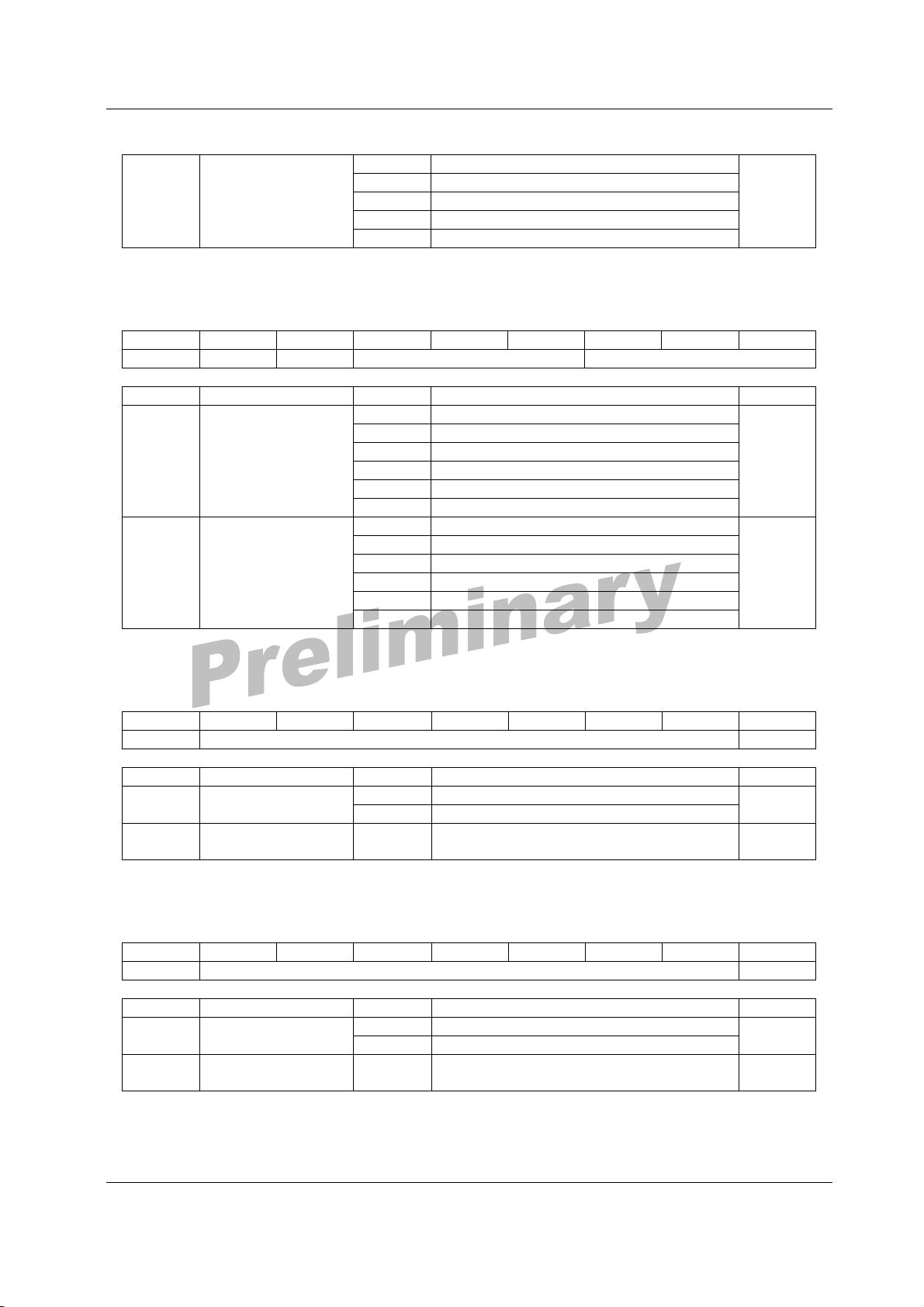
channel for
PWM output port
2B
001 PWM1B is connected to PWM port 2B
010 PWM2A is connected to PWM port 2B
011
PWM2B is connected to PWM port 2B
100 PWM3A is connected to PWM port 2B
101 PWM3B is connected to PWM port 2B
Table 22 Address 0x0D: PWM output port Control for PWM port 3A & 3B
Bit 7 6 5 4 3 2 1 0
Name X X OPM3B OPM3A
Name Description Value Meaning Ref.
000 PWM1A is connected to PWM port 3A
001 PWM1B is connected to PWM port 3A
010 PWM2A is connected to PWM port 3A
011 PWM2B is connected to PWM port 3A
100
PWM3A is connected to PWM port 3A
OPM3A
Select source
channel for
PWM output port
3A
101 PWM3B is connected to PWM port 3A
000 PWM1A is connected to PWM port 3B
001 PWM1B is connected to PWM port 3B
010 PWM2A is connected to PWM port 3B
011 PWM2B is connected to PWM port 3B
100 PWM3A is connected to PWM port 3B
101
PWM3B is connected to PWM port 3B
OPM3B
Select source
channel for
PWM output port
3B
Table 23 Address 0x0E: DRC control for channel 1&2
Bit 7 6 5 4 3 2 1 0
Name CTS CPR
Name Description Value Meaning Ref.
CPR DRC enable
0
1 Dynamic Range Compression on
CTS DRC threshold 57~12dB
Dynamic Range Compression off
Unsigned 6-bit DRC threshold
Refer to DRC threshold value table.
Table 24 Address 0x0F: DRC control for channel 3
Bit 7 6 5 4 3 2 1 0
Name CTS CPR
Name Description Value Meaning Ref.
CPR DRC enable
CTS DRC threshold 57~12dB
0 Dynamic Range Compression off
1 Dynamic Range Compression on
Unsigned 6-bit DRC threshold
Refer to DRC threshold value table.
Copyright © NeoFidelity, Inc. 2005 23
Preliminary datasheet – NeoFidelity reserves the right to change specifications at any time without prior notice
R0.73-11.2006
Page 24

Power Integrated Processor for Digital Amplifier NTP3000
Table 25 Address 0x10: DRC configuration control
Bit 7 6 5 4 3 2 1 0
Name X X C1C A1C
Name Description Value Meaning Ref.
A1C DRC attack rate Attack and release rate
C1C DRC release rate See attack and release rate tables.
Table 26 Address 0x11: Modulation Index & NS-Type Control
Bit 7 6 5 4 3 2 1 0
Name X M0 NT MD3 MD12
Name Description Value Meaning Ref.
MD12
MD3
NT
Modulation index
control by Minimum
pulse width
for Ch 1&2
Modulation index
control by Minimum
pulse width for Ch3
Noise shaping Type
for Ch 1&2 &3
11
10 Minimum pulse width = 4
01 Minimum pulse width = 6
00 Minimum pulse width = 8
11
10 Minimum pulse width = 4
01 Minimum pulse width = 6
00 Minimum pulse width = 8
0 Type 1 4
1
Minimum pulse width = 2
Minimum pulse width = 2
Type 2 5
00 No left shift on dither value = Dither off
M0
Dither Position
Selector
01
10 2bit left shift on dither value
1bit left shift on dither value
11 3bit left shift on dither value
Table 27 Address 0x12: Prescaler Control for Ch 1&2
Bit 7 6 5 4 3 2 1 0
Name PS
Name Description Value Meaning Ref.
PS Prescaler value unsigned 208 default
Table 28 Address 0x13: Prescaler Control for Ch 3
Bit 7 6 5 4 3 2 1 0
Name PS
Name Description Value Meaning Ref.
PS Prescaler value unsigned 208 default
Copyright © NeoFidelity, Inc. 2005 24
Preliminary datasheet – NeoFidelity reserves the right to change specifications at any time without prior notice
R0.73-11.2006
Page 25
Power Integrated Processor for Digital Amplifier NTP3000
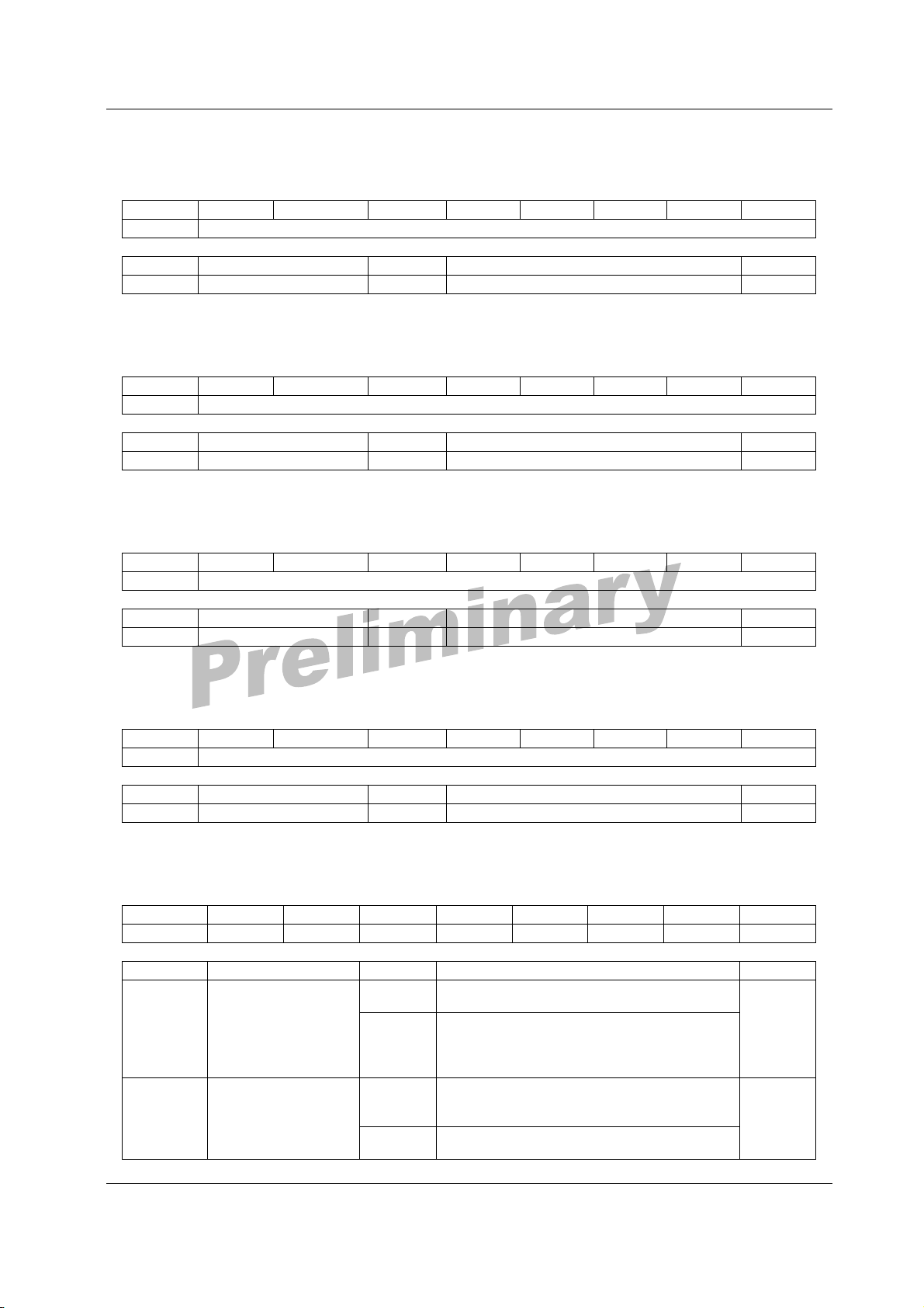
Table 29 Address 0x17: Aout Rising Edge Delay
Bit 7 6 5 4 3 2 1 0
Name ARED
Name Description Value Meaning Ref.
ARED
Aout Rising Edge Delay
unsigned 0 default
Table 30 Address 0x18: Aout Falling Edge Delay
Bit 7 6 5 4 3 2 1 0
Name AFED
Name Description Value Meaning Ref.
AFED
Aout Falling Edge Delay
unsigned 0 default
Table 31 Address 0x19: Bout Rising Edge Delay
Bit 7 6 5 4 3 2 1 0
Name BRED
Name Description Value Meaning Ref.
BRED
Bout Rising Edge Delay
unsigned 0 default
Table 32 Address 0x1A: Bout Falling Edge Delay
Bit 7 6 5 4 3 2 1 0
Name BFED
Name Description Value Meaning Ref.
BFED
Bout falling Edge Delay
unsigned 0 default
Table 33 Address 0x1B: PWM off & Auto PROTECT Control
Bit 7 6 5 4 3 2 1 0
Name 1 0 1 0 1 0 APM POF
Name Description Value Meaning Ref.
0
POF PWM off flag
1
0
APM PROTECT flag
1
Even if Auto PROTECT condition is met, the
PWM output of all channel is not affected.
When Auto PROTECT condition is met, the
PWM output of all channel goes to the defined
state which is set by the PWM off state control
register (Address 0x03 AHL, BHL).
Even if Auto PROTECT condition is met, the
PROTECT output of all channel is not
affected.
When Auto PROTECT condition is met, the
PROTECT output goes to Low state.
Copyright © NeoFidelity, Inc. 2005 25
Preliminary datasheet – NeoFidelity reserves the right to change specifications at any time without prior notice
R0.73-11.2006
Page 26

Power Integrated Processor for Digital Amplifier NTP3000
Table 34 Address 0x1C : Auto PROTECT condition Control Masking
Bit 7 6 5 4 3 2 1 0
Name VMSK3 VMSK2 VMSK1 VMSK0 PMSK3 PMSK2 PMSK1 PMSK0
Name Description Value Meaning Ref.
PMSK
VMSK
Masking bit of
PWM off control
Masking bit of
PROTECT signal
Table 35 Address 0x1D: PROTECT Control
Bit 7 6 5 4 3 2 1 0
Name IR AVRCT PHT
Name Description Value Meaning Ref.
000 0.5 msec Hold Time
001 1 msec Hold Time
PHT
PROTECT Low
Hold Time
010 2 msec Hold Time
011
4 msec Hold Time (Default)
100 8 msec Hold Time
101 16msec Hold Time
000 2
AVRCT
Auto PROTECT
Restore Counter
Threshold
001
010 10
011 15
100 20
101 25
5 (Default)
110 30
111 Infinity
00
2 (Default)
01 4
IRC
Auto PROTECT
Restore Interval
Ratio Control
Table 36 Address 0x1E: PROTECT Control
Bit 7 6 5 4 3 2 1 0
Name 0 0 0 0 SRD FPMLD
PWMM
Name Description Value Meaning Ref.
PWMM
PROTECT
register
Permanent
FPMLD
PROTECT
Low disable flag
SRD FAULT disable
10
otherwise
0
1
0
1 FAULT is ineffective for PROTECT
PROTECT output is low. (reset default)
PROTECT output is high.
No effect
Reset the auto PROTECT restore counter
to 0
FAULT is effect for PROTECT
Copyright © NeoFidelity, Inc. 2005 26
Preliminary datasheet – NeoFidelity reserves the right to change specifications at any time without prior notice
R0.73-11.2006
Page 27

Power Integrated Processor for Digital Amplifier NTP3000
Table 37 Address 0x1F: Switching Off Control
Bit 7 6 5 4 3 2 1 0
Name X X X X X POF3 POF2 POF1
Name Description Value Meaning Ref.
POFn
Switching output
On/off control
0 Channel n PWM switching on
1
Channel n PWM switching off
Table 38 Address 0x20: Softmute Control
Bit 7 6 5 4 3 2 1 0
Name X X X X X SM3 SM2 SM1
Name Description Value Meaning Ref.
SMn Softmute 0 increase for channel n
1
decrease for channel n
Table 39 Address 0x2C: FBQ_FLAG for Ch 1&2&3
Bit 7 6 5 4 3 2 1 0
Name X X FBQ32 FBQ31 FBQ22 FBQ21 FBQ12 FBQ11
Name Description Value Meaning Ref.
FBQ11
FBQ12
FBQ21
FBQ22
FBQ31
FBQ32
1st FBQ flag
for CH1
2nd FBQ flag
for CH1
1st FBQ flag
for CH2
2nd FBQ flag
for CH2
1st FBQ flag
for CH3
2nd FBQ flag
for CH3
0
1 Enable
0
1 Enable
0
1 Enable
0
1 Enable
0
1 Enable
0
1 Enable
Bypass
Bypass
Bypass
Bypass
Bypass
Bypass
Table 40 Address 0x2D: Master Fine volume
Bit 7 6 5 4 3 2 1 0
Name X X X X X MVFC
Name Description Value Meaning Ref.
MVFC
Master volume
fine control
000
~ ~
111 0.5 dB with 0.0625 dB step
0 dB
Copyright © NeoFidelity, Inc. 2005 27
Preliminary datasheet – NeoFidelity reserves the right to change specifications at any time without prior notice
R0.73-11.2006
Page 28

Power Integrated Processor for Digital Amplifier NTP3000
Table 41 Address 0x2E~0x31: Master volume & Channel 1~3 volume respectively
Bit 7 6 5 4 3 2 1 0
Name VOL
Name Description Value Meaning Ref.
See volume control register tables.
VOL Volume control
Reset default is 0 ( = −∞ dB)for Master
and 207 for Channel
Table 42 Address 0x32~0x36: GEQ Gain for Band 2~6
Bit 7 6 5 4 3 2 1 0
Name X X X BG
Name Description Value Meaning Ref.
BG Band Gain See register value table.
Name Address Band Frequency Ref
Band
0x32 Band 2
0x33 Band 3
0x36 Band 4
0x34 Band 5
0x35 Band 6
220Hz
470Hz
1kHz
2.2kHz
4.7kHz
Table 43 Address 0x69 & 0x6A: GEQ Gain for Band 1 & Band 7
Bit 7 6 5 4 3 2 1 0
Name X X X BG
Name Description Value Meaning Ref.
BG Band Gain See register value table.
Name Address Band Frequency Ref
Band
0x69 Band 1
0x6A Band 7
80Hz
12kHz
Table 44 Address 0x37~0x3C: Mixer Gain
Bit 7 6 5 4 3 2 1 0
Name X MG
Name Description Value Meaning Ref.
MG Mixer gain Mixer gain download register
Copyright © NeoFidelity, Inc. 2005 28
Preliminary datasheet – NeoFidelity reserves the right to change specifications at any time without prior notice
R0.73-11.2006
Page 29

Power Integrated Processor for Digital Amplifier NTP3000
Table 45 Address 0x3D~0x3E: Back Biquad Filter Configuration for Ch 1~2 respectively
Bit 7 6 5 4 3 2 1 0
Name BQF5n BQF4n BQF3n BQF2n BQF1n
Name Description Value Meaning Ref.
BQF1n
BQF2n
BQF3n
BQF4n
BQF5n
On/Off biquad 1
of CH n (= CH 1,2,3)
On/Off biquad 2
of CH n (= CH 1,2,3)
On/Off biquad 3
of CH n (= CH 1,2,3)
On/Off biquad 4
of CH n (= CH 1,2,3)
On/Off biquad 5
of CH n (= CH 1,2,3)
0
1 Enable biquad 1 of channel n
0
1 Enable biquad 2 of channel n
00
01 Enable biquad 3 of channel n
10 Enable biquad 3 as Loudness Filter
00
01 Enable biquad 4 of channel n
10 Enable biquad 4 as Loudness Filter
00
01 Enable biquad 5 of channel n
10 Enable biquad 5 as Loudness Filter
Bypass biquad 1 of channel n
Bypass biquad 2 of channel n
Bypass biquad 3 of channel n
Bypass biquad 4 of channel n
Bypass biquad 5 of channel n
Table 46 Address 0x3F: Biquad Filter Coefficient Page
Bit 7 6 5 4 3 2 1 0
Name CH3L Various2 Various1
3D GEQ2 GEQ1 CH2 CH1
Name Description Value Meaning Ref.
CHn Write enable
GEQ1
GEQ2
3D
Various1
Various2
CH3L
Write enable for
GEQ UD mode Ch1
Write enable for
GEQ UD mode CH2
Write enable for
3D filter
Write enable for
FBQ, ALC
Write enable for FBQ
and BBQ of CH3
Write enable for
CH3 Loudness gain
0
1 Enable Channel n coefficient write
0
1 Enable coefficient write
0
1 Enable coefficient write
0
1 Enable coefficient write
0
1 Enable coefficient write
0
1 Enable coefficient write
0
1 Enable coefficient write
Disable channel n coefficient write
Disable coefficient write
Disable coefficient write
Disable coefficient write
Disable coefficient write
Disable coefficient write
Disable coefficient write
Table 47 Address 0x40~0x58: Biquad Filter Coefficient
32-bit floating point
Table 48 Address 0x59~0x5B: Loudness Gain for BQ 3,4,5 of Ch 1& 2 &3
32-bit floating point
Table 49 Address 0x5C~0x5F: Mixer Gain value for 3D
32bit floating point
Copyright © NeoFidelity, Inc. 2005 29
Preliminary datasheet – NeoFidelity reserves the right to change specifications at any time without prior notice
R0.73-11.2006
Page 30
Power Integrated Processor for Digital Amplifier NTP3000
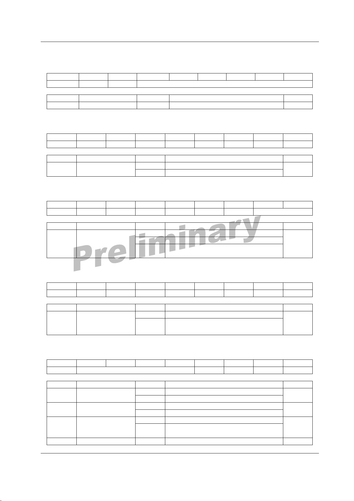
Table 50 Address 0x60: 3D delay amount
Bit 7 6 5 4 3 2 1 0
Name X X 3D_Delay
Name Description Value Meaning Ref.
3D_Delay
3D_Delay
unsigned
1 ~ 40
Table 51 Address 0x61 3D effect control configuration
Bit 7 6 5 4 3 2 1 0
Name X X X X X X X 3BF
Name Description Value Meaning Ref.
3BF 3D Bypass Flag
0
1 3D on
Bypass
Table 52 Address 0x62 PWM Mode Control Register
Bit 7 6 5 4 3 2 1 0
Name X X X X X X PM
Name Description Value Meaning Ref.
PM PWM Mode
00
01 1 chip, 2.1 channel mode
10
Forbidden. Must be set as below.
1 chip 2.0 channel mode or 2.1 channel
with external power stage
Table 52 Address 0x63 Stand-by in 2 Channel mode
Bit 7 6 5 4 3 2 1 0
Name X X X X X X X SB
Name Description Value Meaning Ref.
SB
stand-by in
2 Channel mode
0
1 Normal operation
Stand-by operation
Table 53 Address 0x75: System Status (Read-only)
Bit 7 6 5 4 3 2 1 0
Name FSI MPW LSRC ULCK PPM
Name Description Value Meaning Ref.
ULCK
MPW
PPM
sampled PLL
unlock error
MCK/WCK
ratio error
Permanent
PROTECT
Indication flag
0 PLL is locked state.
1 PLL is unlocked state.
0 Ratio is incorrect.
1 Ratio is correct.
0
1
Indicated that PROTECT is in Permanent LOW
state
LSRC ASRC lock status 0 ASRC is unlocked state.
Copyright © NeoFidelity, Inc. 2005 30
Preliminary datasheet – NeoFidelity reserves the right to change specifications at any time without prior notice
R0.73-11.2006
Page 31
Power Integrated Processor for Digital Amplifier NTP3000
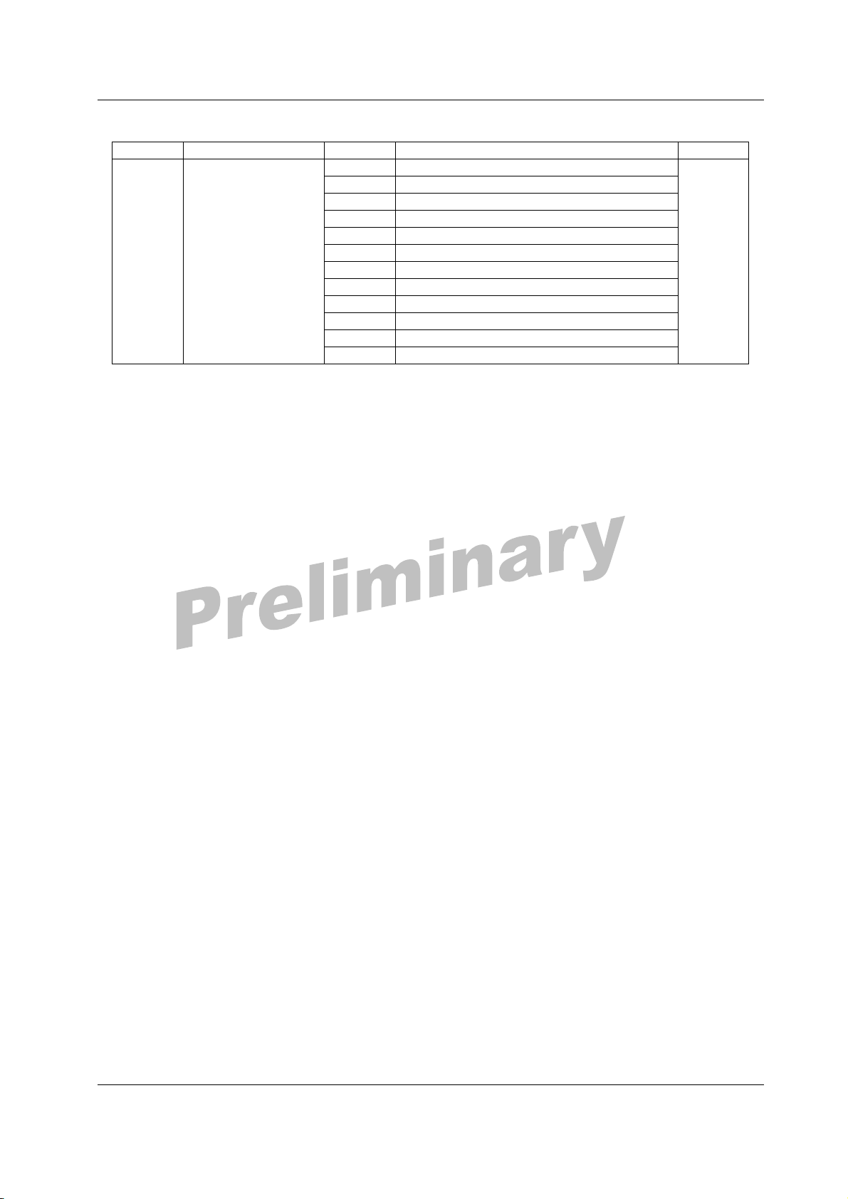
1 ASRC is locked state.
0000 8kHz
0001 11.025kHz
0010 12kHz
0011 16kHz
0100 24kHz
0101 24 kHz
0110 32 kHz
0111 44.1 kHz
FSI
Sampling
Frequency
Information
1000 48 kHz
1001 88.2 kHz
1010 96 kHz
1011 192 kHz
Copyright © NeoFidelity, Inc. 2005 31
Preliminary datasheet – NeoFidelity reserves the right to change specifications at any time without prior notice
R0.73-11.2006
Page 32

Power Integrated Processor for Digital Amplifier NTP3000
FE
FA
F9
F6
F5
F4
F3
F2
EE
ED
EA
E9
E8
E7
E6
E2
E1
DE
DD
DC
DB
DA
D6
A2. Configuration Register Value Reference
Master & Channel Volume
Index
dB Index dB Index dB Index dB Index dB Index dB
FF 24.0
23.5
FD 23.0
FC 22.5
FB 22.0
21.5
21.0
F8 20.5
F7 20.0
19.5
19.0
18.5
18.0
17.5
F1 17.0
F0 16.5
EF 16.0
15.5
15.0
EC 14.5
EB 14.0
13.5
13.0
12.5
12.0
11.5
E5 11.0
E4 10.5
E3 10.0
9.5
9.0
E0 8.5
DF 8.0
7.5
7.0
6.5
6.0
5.5
D9 5.0
D8 4.5
D7 4.0
3.5
D5 3.0
D4 2.5
D3 2.0
D2 1.5
D1 1.0
D0 0.5
CF 0.0
CE -0.5
CD -1.0
CC -1.5
CB -2.0
CA -2.5
C9 -3.0
C8 -3.5
C7 -4.0
C6 -4.5
C5 -5.0
C4 -5.5
C3 -6.0
C2 -6.5
C1 -7.0
C0 -7.5
BF -8.0
BE -8.5
BD -9.0
BC -9.5
BB -10.0
BA -10.5
B9 -11.0
B8 -11.5
B7 -12.0
B6 -12.5
B5 -13.0
B4 -13.5
B3 -14.0
B2 -14.5
B1 -15.0
B0 -15.5
AF -16.0
AE -16.5
AD -17.0
AC -17.5
AB -18.0
AA -18.5
A9 -19.0
A8 -19.5
A7 -20.0
A6 -20.5
A5 -21.0
A4 -21.5
A3 -22.0
A2 -22.5
A1 -23.0
A0 -23.5
9F -24.0
9E -24.5
9D -25.0
9C -25.5
9B -26.0
9A -26.5
99 -27.0
98 -27.5
97 -28.0
96 -28.5
95 -29.0
94 -29.5
93 -30.0
92 -30.5
91 -31.0
90 -31.5
8F -32.0
8E -32.5
8D -33.0
8C -33.5
8B -34.0
8A -34.5
89 -35.0
88 -35.5
87 -36.0
86 -36.5
85 -37.0
84 -37.5
83 -38.0
82 -38.5
81 -39.0
80 -39.5
7F -40.0
7E -40.5
7D -41.0
7C -41.5
7B -42.0
7A -42.5
79 -43.0
78 -43.5
77 -44.0
76 -44.5
75 -45.0
74 -45.5
73 -46.0
72 -46.5
71 -47.0
70 -47.5
6F -48.0
6E -48.5
6D -49.0
6C -49.5
6B -50.0
6A -50.5
69 -51.0
68 -51.5
67 -52.0
66 -52.5
65 -53.0
64 -53.5
63 -54.0
62 -54.5
61 -55.0
60 -55.5
5F -56.0
5E -56.5
5D -57.0
5C -57.5
5B -58.0
5A -58.5
59 -59.0
58 -59.5
57 -60.0
56 -60.5
55 -61.0
54 -61.5
53 -62.0
52 -62.5
51 -63.0
50 -63.5
4F -64.0
4E -64.5
4D -65.0
4C -65.5
4B -66.0
4A -66.5
49 -67.0
48 -67.5
47 -68.0
46 -68.5
45 -69.0
44 -69.5
43 -70.0
42 -70.5
41 -71.0
40 -71.5
3F -72.0
3E -72.5
3D -73.0
3C -73.5
3B -74.0
3A -74.5
39 -75.0
38 -75.5
37 -76.0
36 -76.5
35 -77.0
34 -77.5
33 -78.0
32 -78.5
31 -79.0
30 -79.5
2F -80.0
2E -80.5
2D -81.0
2C -81.5
2B -82.0
2A -82.5
29 -83.0
28 -83.5
27 -84.0
26 -84.5
25 -85.0
24 -85.5
23 -86.0
22 -86.5
21 -87.0
20 -87.5
1F -88.0
1E -88.5
1D -89.0
1C -89.5
1B -90.0
1A -90.5
19 -91.0
18 -91.5
17 -92.0
16 -92.5
15 -93.0
14 -93.5
13 -94.0
12 -94.5
11 -95.0
10 -95.5
0F -96.0
0E -96.5
0D -97.0
0C -97.5
0B -98.0
0A -98.5
09 -99.0
08 -99.5
07 -100
06 -110
05 -120
04 -130
03 -140
02 -150
01 -150
00 -150
Copyright © NeoFidelity, Inc. 2005 32
Preliminary datasheet – NeoFidelity reserves the right to change specifications at any time without prior notice
R0.73-11.2006
Page 33
Power Integrated Processor for Digital Amplifier NTP3000
6C
66
64
62
60
5A
58
56
50
4E
4C
4A
44
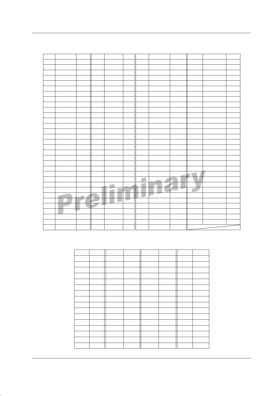
Mixer Gain & Polarity
Index
Polarity dB Index Polarity dB
7E
7C
7A
78
76
74
72
70
6E
6A
68
5E
5C
54
52
48
46
42
40
+ 18 7D - 18
+ 17 7B - 17
+ 16 79 - 16
+ 15 77 - 15
+ 14 75 - 14
+ 13 73 - 13
+ 12 71 - 12
+ 11 6F - 11
+ 10 6D - 10
+ 9 6B - 9 2C + -11 2B - -11
+ 8 69 - 8 2A + -12 29 - -12
+ 7 67 - 7 28 + -13 27 - -13
+ 6 65 - 6 26 + -14 25 - -14
+ 5.5
+ 5 61 - 5 22 + -16 21 - -16
+ 4.5
+ 4 5D - 4 1E + -18 1D - -18
+ 3.5
+ 3 59 - 3 1A + -20 19 - -20
+ 2.5
+ 2 55 - 2 16 + -22 15 - -22
+ 1.5
+ 1 51 - 1 12 + -24 11 - -24
+ 0.5
+ 0 4D - 0 0E + -26 0D - -26
+ -0.5
+ -1 49 - -1
+ -1.5
+ -2 45 - -2
+ -2.5
+ -3 41 - -3
+ -3.5
63 - 5.5
5F - 4.5
5B - 3.5
57 - 2.5
53 - 1.5
4F - 0.5
4B - -0.5
47 - -1.5
43 - -2.5
3F - -3.5
Index Polarity dB Index Polarity dB
3E + -4
3C + -4.5
3A + -5
38 + -5.5
36 + -6
34 + -7
32 + -8
30 + -9
2E + -10 2D - -10
24 + -15 23 - -15
20 + -17 1F - -17
1C + -19 1B - -19
18 + -21 17 - -21
14 + -23 13 - -23
10 + -25 0F - -25
0C + -27 0B - -27
0A + -28 09 - -28
08 + -29 07 - -29
06 + -30 05 - -30
04 + -31 03 - -31
02 + -32 01 - -32
00 + -150
3D - -4
3B - -4.5
39 - -5
37 - -5.5
35 - -6
33 - -7
31 - -8
2F - -9
Dynamic Range Compression Threshold
Index
3F -57.0
3E -54.0
3D -51.0
3C -48.0
3B -45.0
3A -42.0
39 -39.0
38 -36.0
37 -33.0
36 -30.0
35 -27.0
34 -24.0
33 -21.0
32 -18.0
31 -15.0
30 -12.0
dB Index
2F -11.5
2E -11.0
2D -10.5
2C -10.0
2B -9.5
2A -9.0
29 -8.5
28 -8.0
27 -7.5
26 -7.0
25 -6.5
24 -6.0
23 -5.5
22 -5.0
21 -4.5
20 -4.0
dB Index
1F -3.5
1E -3.0
1D -2.5
1C -2.0
1B -1.5
1A -1.0
19 -0.5
18 0
17 0.5
16 1.0
15 1.5
14 2.0
13 2.5
12 3.0
11 3.5
10 4.0
dB Index dB
0F 4.5
0E 5.0
0D 5.5
0C 6.0
0B 6.5
0A 7.0
09 7.5
08 8.0
07 8.5
06 9.0
05 9.5
04 10.0
03 10.5
02 11.0
01 11.5
00 12.0
Copyright © NeoFidelity, Inc. 2005 33
Preliminary datasheet – NeoFidelity reserves the right to change specifications at any time without prior notice
R0.73-11.2006
Page 34
Power Integrated Processor for Digital Amplifier NTP3000
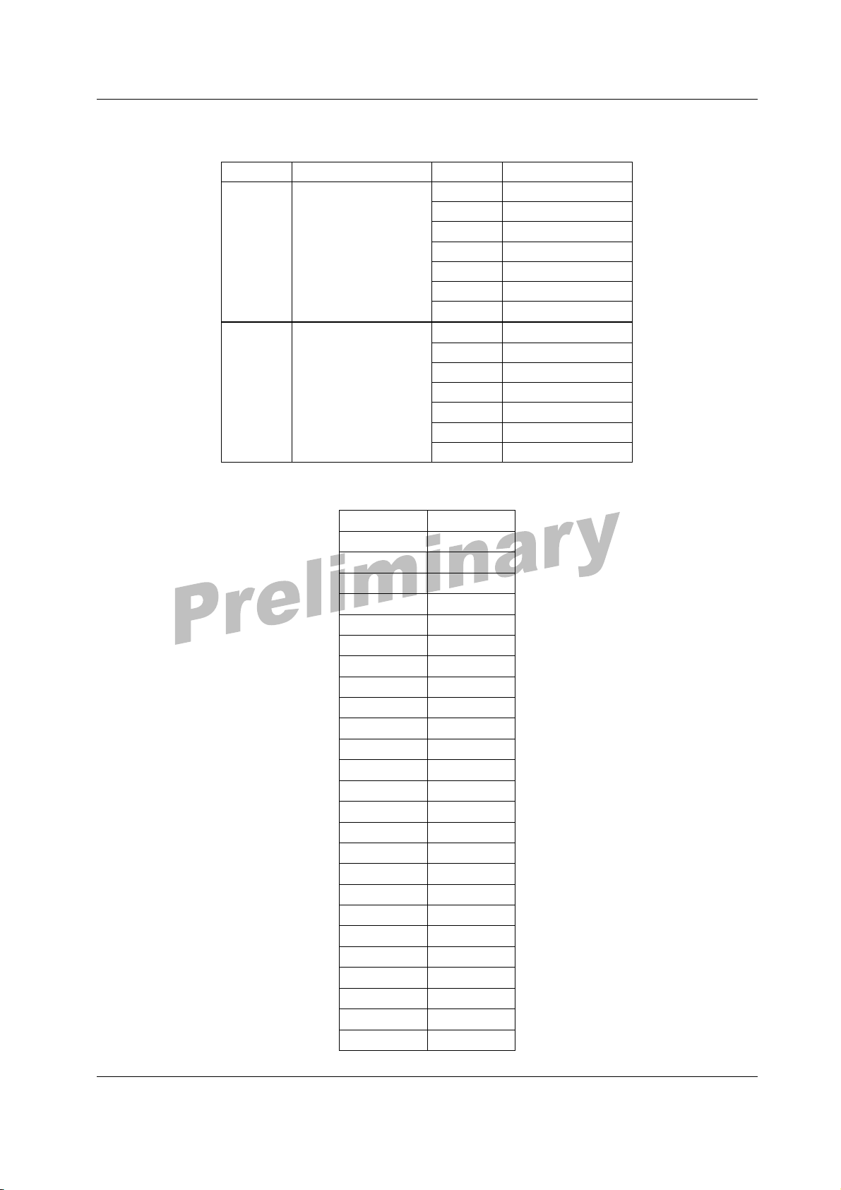
DRC Attack Rate & Release Rate Table
Name Description value rate
011 14.458 (slowest)
010 7.292
001 3.646
000 1.823 (default)
111 0.906
110 0.448
101 0.219 (fastest)
011 7.3
010 5.5
001 4.4
000 3.6
111 2.7
110 1.8
101 0.9
A1C
C1C
DRC attack rate
(msec/3dB down)
DRC release rate
(sec/6dB up)
Graphic Equalizer Band Gain
Value(HEX)
14 -12
15 -11
16 -10
17 -9
18 -8
19 -7
1A -6
1B -5
1C -4
1D -3
1E -2
1F -1
00 0
01 1
02 2
03 3
04 4
05 5
06 6
07 7
08 8
09 9
0A 10
0B 11
0C 12
dB
Copyright © NeoFidelity, Inc. 2005 34
Preliminary datasheet – NeoFidelity reserves the right to change specifications at any time without prior notice
R0.73-11.2006
Page 35

Power Integrated Processor for Digital Amplifier NTP3000
Auto-mute detection threshold Table
Name Description value
0000
0001
0010
0011
0100
0101
0110
AT
Auto-mute
Detection
threshold
0111
1000
1001
1010
1011
1100
1101
1110
1111 Auto-mute
㏈
-126 ㏈
-120 ㏈
-114 ㏈
-108 ㏈
-102 ㏈
-96 ㏈
-90 ㏈
-84 ㏈
-78 ㏈
-72 ㏈
-66 ㏈
-60 ㏈
-54 ㏈
-48 ㏈
-42 ㏈
※※※※ Do not use value 1111.
Copyright © NeoFidelity, Inc. 2005 35
Preliminary datasheet – NeoFidelity reserves the right to change specifications at any time without prior notice
R0.73-11.2006
Page 36
Power Integrated Processor for Digital Amplifier NTP3000
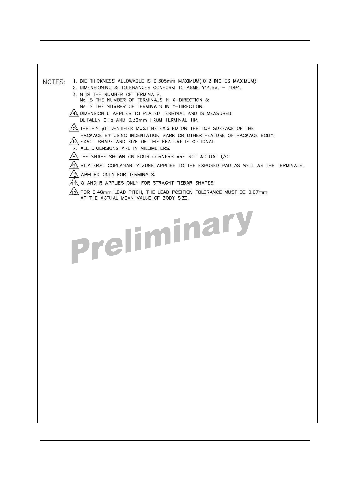
A3. Outline and Mechanical Data
Copyright © NeoFidelity, Inc. 2005 36
Preliminary datasheet – NeoFidelity reserves the right to change specifications at any time without prior notice
R0.73-11.2006
Page 37
Power Integrated Processor for Digital Amplifier NTP3000
Copyright © NeoFidelity, Inc. 2005 37
Preliminary datasheet – NeoFidelity reserves the right to change specifications at any time without prior notice
R0.73-11.2006
 Loading...