


NEL SR-A29B0 User Manual
查询SR-A29B1-FREQ供应商
Differential Positive ECL (DPECL)
SR-A29B0
Series
Size, mm
9 x 14
I/O
8 pad
Supply Voltage
3.3V / 2.5V
• Patent Pending, harmonic
multiplication for
extremely low jitter
• High frequency output
eliminates the need for
PLL multiplication
• Stabilities over
temperatures as low as
±20ppm eliminates SAW
oscillator temperature
problems
SR-A29B0 Series Rev G
Frequency Range: 250.0 MHz-1.7 GHz
Description
The SR-A29B0 Series of quartz crystal oscillators provide DPECL Fast Edge compatible
signals. This device is to operate using positive voltage and uses multiple ground pins for
improved signal integrity. This device is intended to operate on positive voltage for PECL
applications.
Features
• Wide frequency range – 250.0MHz to
1.7GHz
• User specified tolerance available
• Will withstand SMD reflow temperatures of
183°C for 4 minutes maximum
• High shock resistance, to 1000g
Creating a Part Number
SR - A29BX - FREQ
Package Code
SR 8 pad 9x14 mm SMD
Input Voltage
Code Specification
A 3.3 V
B 2.5 V
Drawing Specifications
• High Reliability - NEL HALT/HASS
qualified for crystal oscillator start-up
conditions
• Cover connected to ground
• 3.3V and 2.5V versions available
Tolerance/Performance
0 ±100 ppm 0-70°C
1 ±50 ppm 0-70°C
7 ±25 ppm 0-70°C
9 Customer Specific
A ±20 ppm 0-70°C
B ±50 ppm -40 to +85°C
C ±100 ppm -40 to +85°C
For the most up to date
specifications on each NEL
product, log on to our
website—www.nelfc.com
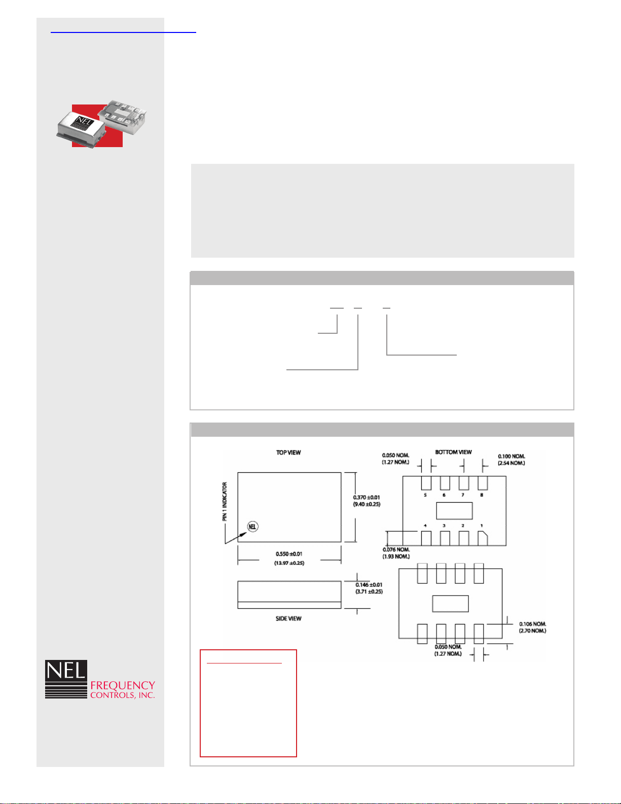
Electrical Connections
Pin Connection
1 V
2 Ground
3 NC or Ground
4 Q Output
5 /Q Output
6 Ground
7 Ground
8 Enable
357 Beloit Street, P.O. Box 457, Burlington, WI 53105-0457 U.S.A.
Phone: 262-763-3591 Fax: 262-763-2881 Email: nelsales@nelfc.com www.nelfc.com
CC
Recommended Board Layout
Dimensions shown in inches (mm).
The metallic center pad was designed for
mechanical support. Grounding of this pad is
optional. It measures 0.088 x 0.190 NOM
(2.24 x 4.83 NOM).

Differential Positive ECL (DPECL)
SR-A29B0 Series Rev G
Frequency Range: 250.0 MHz-1.7 GHz
Operating Conditions and Output Characteristics
Electrical Characteristics
Parameter Symbol Conditions Min Typical Max
Frequency — — 250.0MHz — 1.7GHz
Duty Cycle — @ 50% points 45/55% — 55/45%
Logic 0
Logic 1
Rise & Fall Time
RMS Random Jitter
Enable Voltage
Disable Voltage — with VEE=0V 3.0V — V
Frequency Stability
voltage, calibration, temp.,
10 yr aging, shock, vibration
Phase Noise
— @1kHz — — -115 dBc/Hz
— @10kHz — — -130 dBc/Hz
— @100kHz — — -130 dBc/Hz
— @1MHz — — -135 dBc/Hz
— @10MHz — — -135 dBc/Hz
(1)
VOL — V
(1)
VOH — V
(5)
— — — — 1 psec
(2)
— with VEE=0V 0V — 1.0V
(3)
dF/F Overall conditions including: -100ppm — +100ppm
(4)
— @100Hz — — -80 dBc/Hz
t
r, tf 20-80%VO with 50 ohm load to V
CC
-1.810V — V
CC
-1.025V — V
CC
-2V — 350 psec 600 psec
-1.620V
CC
-0.880V
CC
CC
General Characteristics
Parameter Symbol Conditions Min Typical Max
Supply Voltage VCC — 3.135 V 3.3 V 3.465 V
Supply Current ICC 50 ohm termination 0.0 mA — 120 mA
to 2.00V below V
CC
Output Current IO Low level Output Current 0.0 mA — ±50.0 mA
Operating Temperature TA — 0ºC — 70ºC
Storage Temperature TS — -55ºC — 125ºC
Input: Logic High (ECL) - Disables
VEE or Open - Enables
Lead Temperature TL Soldering, 10 sec. — — 300ºC
Load 50 ohm to V
-2V or Thevenin Equivalent, Bias Required
CC
Start-up Time tS — — 2 ms 10 ms
Environmental and Mechanical Characteristics
Mechanical Shock Per MIL-STD-202, Method 213, Condition E
Thermal Shock Per MIL-STD-833, Method 1011, Condition A
Vibration 0.060" double amplitude 10 Hz to 55 Hz, 35g’s 55 Hz to 2000 Hz
Soldering Condition 300ºC for 10 seconds
Footnotes:
1) VOL, VOH, referenced to ground.
2) Open to enable pin also enables the output.
3) Standard frequency stability (others available).
4) Phase Noise characterization available. Phase Noise is frequency dependent,
phase noise specification references a 1.0GHz part.
5) RMS jitter bandwidth of 12kHz to 20MHz.