

NEL PJ-A3670 User Manual
查询PJ-A3679-70.0供应商
VCXO Series (PECL)
PJ-A3670
Series
Size, mm
9 x 14
I/O
6 J Lead
Supply Voltage
3.3V
PJ-A3670 Series R
requency Range: 70.0 MHz to 200.0 MHz
F
ev J
Description
The PJ-A3670 Series of voltage controlled quartz crystal oscillators provide frequency control by applying a
voltage to Pin 1. This unit supplies ECLiPS compatible outputs which are enabled when Pin 2 is set to a logic
ow or left open.
l
Features
• High Reliability - NEL HALT/HASS qualified for
crystal oscillator start-up conditions
• Low jitter - Wavecrest jitter characterization available
• Frequency range—70.0 MHz to
200.0 MHz
• Will withstand vapor phase temperatures of 253
for 4 minutes maximum
• Space-saving alternative to discrete component
oscillators
• Wide Absolute Pull Range
• High shock resistance, to 3000g
• 3.3 Volt operation
• Metal lid electrically connected to ground to
reduce EMI
• High Q crystal actively tuned oscillator circuit
• Power supply decoupling internal
• No internal PLL
°C
• High frequencies due to proprietary design
• Gold plated leads—Solder dipped leads available
upon request
• RoHS Compliant, Lead Free Construction
(unless solder dipped leads are supplied)
avoids cascading PLL problems
Creating a Part Number
PJ - A367X - FREQ
Package Code
PJ 6 J Lead 9x14 SMD
APR/Performance
Input Voltage
Code Specification
A 3.3 V
0 ±100 ppm 0-70°C
9 Customer Specific
C ±100 ppm -40 to +85°C
For the most up to date specifications on each NEL product, log on to our website—
www.nelfc.com
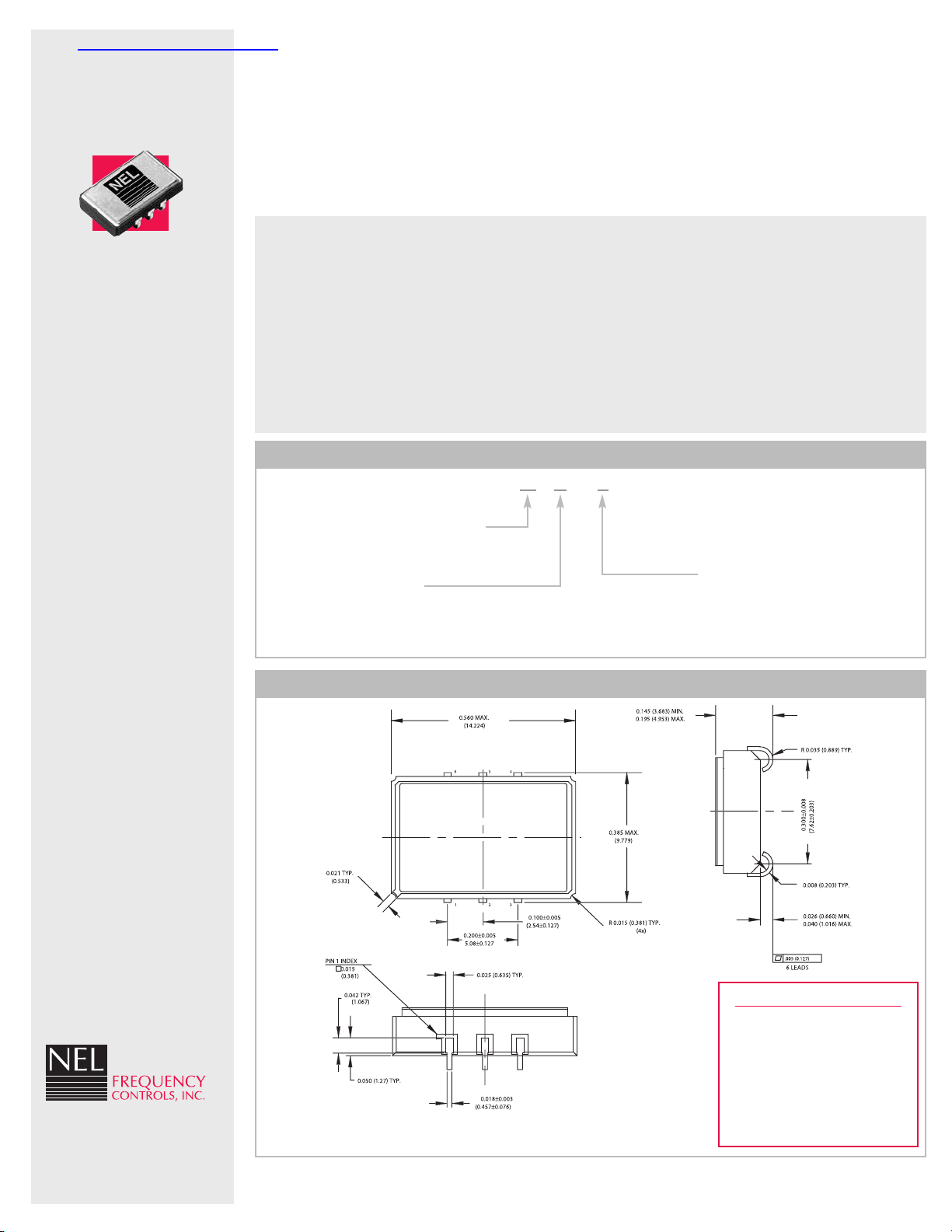
Dimensions shown in inches and millimeters.
urlington,
x 457, B
.O. Bo
eet, P
tr
eloit S
357 B
ax: 262-763-2881 E
F
mail: nelsales@nelfc.com www
Drawing Specifications
WI 53105-0457 U.S.A. P
.nelfc.com
hone: 262-763-3591
Electrical Connection
Pin Connection
1V
2 Output Enable
3
4 Output
5 Output Complement
6
CO
V
EE
V
CC

VCXO Series (PECL)
PJ-A3670 Series
Rev J
Frequency Range: 70.0 MHz to 200.0 MHz
Operating Conditions and Output Characteristics
Electrical Characteristics
Parameter Symbol Conditions Min Typical Max
Frequency — — 70.0 MHz — 200.0 MHz
Duty Cycle — @VO/2 45/55% — 55/45%
Logic 0 V
Logic 1 V
Rise & Fall Time tr, t
Jitter, RMS
(1)
L
O
H
O
f
— — — 3 psec —
Absolute Pull Range APR V
—V
—V
20-80% V
=0.3 to 3.0 V ±100 ppm — —
O
C
O
-1.810 V
C
C
-1.200 V
C
C
C
D
C
D
—V
—V
— — 600 ps
-1.620 V
C
C
-0.880 V
C
C
VCOInput Impedance — 50 na dc current max 100K ohm — —
V
Linearity — V
O
C
Transfer Function
(2)
—V
=0.3 to 3.0 V — — 10%
O
C
=0.3 to 3.0 V — Positive —
O
C
General Characteristics
Parameter Symbol Conditions Min Typical Max
Supply Voltage V
Supply Current I
Output Current I
Operating Temperature T
Storage Temperature T
Power Dissipation P
Lead Temperature T
Load 50 ohm to VCC-2 V or Thevenin Equivalent, Bias Required — — —
-V
C
E
C
E
CC
O
A
S
D
L
Nominal 3.135 V 3.3 V 3.465 V
— — — 60 mA
— 0.0 mA — ±50.0 mA
—0
º
C—70
º
C
— -55ºC — 125ºC
— — — 208 mW
Soldering, 10 sec. — — 300ºC
C
D
C
D
Environmental and Mechanical Characteristics
Mechanical Shock Per MIL-STD-202, Method 213, Condition E
Thermal Shock Per MIL-STD-833, Method 1011, Condition A
Vibration 0.060" double amplitude 10 Hz to 55 Hz, 35g’s 55 Hz to 2000 Hz
Soldering Condition 300ºC for 10 seconds
Hermetic Seal Leak rate less than 1 x 10
Footnotes:
1) Jitter performance is frequency dependent. Please contact factory for full Wavecrest characterization.
RMS jitter bandwidth of 12kHz to 20MHz.
2) Frequency increase with increase in control voltage and is monotonic.
-8
atm.cc/sec of helium
 Loading...