

Page 1
User’s Manual
Line Scan Camera
Type: XCM4085TLCT6
NIPPON ELECTRO-SENSORY DEVICES CORPORATION
Page 2

2 NED
For Customers in the U.S.A.
This equipment has been tested and found to comply with the limits for a Class A
digital device, in accordance with Part 15 of the FCC Rules. These limits are designed
to provide reasonable protection against harmful interference when the equipment is
operated in a commercial environment. This equipment generates, uses, and can
radiate radio frequency energy and, if not installed and used in accordance with the
instruction manual, may cause harmful interference to radio communications.
Operation of this equipment in a residential area is likely to cause harmful interference,
in which case the user will be required to correct the interference at his or her own
expense.
For Customers in the EU
This equipment has been tested and found to comply with the essential
requirements of the EMC Directive 2004/108/EC, based on the following
specifications applied:
EU Harmonized Standards
EN55022:2010 Class A
EN61000-6-2:2005
Warning
This is a class A product. In a domestic environment this product may cause radio
interference in which case the user may be required to take adequate measures.
Directive on Waste Electrical and Electronic Equipment (WEEE)
Please return all End of Life NED products to the distributor from whom the product
was purchased for adequate recycling and / or disposal. All costs of returning the
Product to NED are borne by the shipper.
XCM4085TLCT6 UME-0062-01
Page 3
3 NED
Warning
If the product is not handled properly, this may result
in serious injury or possible death.
Caution
If the product is not handled properly, this may result
in physical injury or cause property damage.
Warning
Introduction
Thank you for purchasing NED’s Line Scan Camera. We look forward to your
continued custom in the future.
For safety use
For your protection, please read these safety instructions completely before
operating the product and keep this manual for future reference.
The following symbols appear next to important information regarding safe
product handling.
Safety precaution
Never disassemble or modify this product, unless otherwise specified to do so in
this manual.
When hands are wet, avoid handling this product and do not touch any of the
connection cable pins or other metallic components.
Do not operate this product in an environment that is exposed to rain or other
severe external elements, hazardous gases or chemicals.
If the product is not to be used for an extended period of time, as a safety
precaution, always unplug the connection cable from the camera unit.
If the product installation or inspection must be executed in an overhead location,
please take the necessary measures to prevent the camera unit and its
components from accidentally falling to the ground.
If smoke, an abnormal odor or strange noise is emitted from the camera unit, first
turn OFF power, then unplug the cable from the camera unit.
This product is not intended for use in a system configuration built for critical
applications.
XCM4085TLCT6 UME-0062-01
Page 4

4 NED
Instructions before use
Only operate this product within the recommended environmental temperature
range.
Use only the specified power source and voltage rating.
Do not drop this product. Avoid exposure to strong impact and vibrations.
Install the camera unit in a well-ventilated environment, in order to prevent the
camera from overheating.
If the camera must be installed in an environment containing dust or other
particles, take required measures to protect the camera unit from dust adhesion.
Do not unplug the cable while power is being supplied to the camera unit. To
prevent product damage, always shut down the power supply before unplugging
the power cable.
When the surface of the camera window becomes dirty due to dust or grime, black
smudges appear in the displayed image. Use an air blower to remove the dust
particles. Dip a cotton swab into ethanol alcohol and clean the camera window. Be
careful not to scratch the glass.
Use of non-infrared lighting such as a fluorescent lamp is recommended. If
halogen lighting is employed, always install an infrared filter into your system
configuration.
Please note that exposure to long wavelength light outside of the sensors visible
optical range can affect the image.
Sensitivity may fluctuate depending on the spectral response level of the light
source. In cases like this, changing the light source to one with a different spectral
response level may reduce this problem.
Do not expose the sensor to excessive amount of light. The exposure of
excessive amount of light causes a saturated output and other harmful unwanted
characteristics.
Suitable measures should be taken to protect the colour filter on sensor from
bright light when it is not in use.
If the sensor is continually exposed to excessive amount of light over time, the
colour filter may become faded.
For stabilized image capturing, turn ON the power supply and execute aging for
ten to twenty minutes before actually using the camera unit.
Do not share the power supply with motor units or other devices that generate
noise interference.
The signal ground (SG) and the frame ground (FG) are connected inside the
camera unit. Design the system configuration so that a loop will not be formed by
the ground potential differential.
Do not disconnect the camera while rewriting an embedded memory.
When you change exposure mode that is set at NED factory, input control signal
(CC1) from the capture board.
XCM4085TLCT6 UME-0062-01
Page 5

5 NED
Product Warranty
Warranty Period
The product warranty period, as a general rule, is two years from purchase;
however for detailed conditions please contact the sales representative for your
region/country.
However, in some cases due to the usage environment, usage conditions and/or
frequency of use, this warranty period may not be applicable.
Warranty Scope
Product repair will be performed on a Return To Manufacturer basis. On-site
maintenance will incur additional charges.
If defects in material or workmanship occur during the warranty period, the faulty
part will be replaced or repaired by us free of charge. Return shipping charges
must be paid by the sender. However, the following cases fall outside of the scope
of this warranty:
Exclusions from Warranty Coverage
We will under no circumstances assume responsibility for the following cases:
damage caused by fire, earthquake, other acts of a third party, other accidents,
negligent or intentional misuse by the user, or other usage under extraordinary
circumstances.
Damages (e.g. loss of business profits, business interruption, etc.) resulting from
use or non-use.
Damages caused by use other than as described in this document.
Damages resulting from malfunction due to a connected device.
Damages resulting from repairs or modifications performed by the customer.
Fault Diagnosis
As a general rule, in the first instance fault diagnosis should take the form of a
telephone call or an email to enable us to assess the circumstances of the
malfunction.
However, depending on the customer’s requests, we, or our agent, may require
an additional fee for this service.
Exclusion of Liability for Compensation for Missed Opportunities
Regardless of whether within the warranty period or not, our warranty does not
cover compensation for missed opportunities for our customers, or our customers’
customers, caused by a fault of our products, nor for damage to products other
than our own, or related business.
XCM4085TLCT6 UME-0062-01
Page 6

6 NED
Note about Product Usage
This product has been designed and manufactured as a general-purpose product
for general industry. In applications expected to be life-critical or safety-critical, the
installer or user is requested to install double or triple failsafe systems.
Repair Service Outline
The cost of dispatching engineers etc. for repair service is not included in the price
of purchased and supplied goods. On request, arrangements can be made
separately.
Scope of Repair Service
The above assumes business dealings and usage to take place in the customer’s
region / country. In cases of business dealings and/or usage outside the
customer’s region/country, separate consultation is required.
XCM4085TLCT6 UME-0062-01
Page 7

7 NED
Table of Contents
1. Product Outline ................................................................... 10
1.1 Features(XCM4085TLCT6) ................................................................................................... 10
1.2 Application ................................................................................................................................ 10
1.3 Image Sensor ............................................................................................................................ 11
1.4 Performance Specifications .................................................................................................... 11
2. Camera Setting and Optical Interface ............................... 13
2.1 Setting the Camera ................................................................................................................... 13
2.2 Fixing the Camera..................................................................................................................... 13
2.3 Optical Interface ........................................................................................................................ 14
3. Hardware .............................................................................. 15
3.1 Camera Connection .................................................................................................................. 15
3.2 Input / Output Connectors and Indicator ............................................................................... 17
3.3 Connectors・Pin Assignments・Cables ................................................................................... 18
3.4 Power Supply ............................................................................................................................ 22
4 Camera Control .................................................................... 23
4.1 Flow of Camera Control ........................................................................................................... 23
4.1.1 Command Overview ..........................................................................................................23
4.1.2 Camera Receiving Message (PC Sending Command) ...................................................23
4.1.3 Camera Sending Message (PC Receiving Message) .....................................................24
4.1.4 Camera Control Commands .............................................................................................25
4.1.5 Memory Setup Values (Factory Settings) ........................................................................27
4.2 Details on Commands .............................................................................................................. 28
4.2.1 Setting Analog Gain ...........................................................................................................28
4.2.2 Setting Digital Gain (1) ......................................................................................................28
4.2.3 Setting Digital Gain (2) ......................................................................................................29
4.2.4 Setting Digital Gain (3) ......................................................................................................29
4.2.5 Setting Digital Offset..........................................................................................................29
4.2.6 Setting Exposure Mode .....................................................................................................29
4.2.7 Setting Exposure Time ......................................................................................................30
4.2.8 Setting Data Output Clock Frequency .............................................................................30
4.2.9 Setting Data Output Tap Number .....................................................................................30
4.2.10 Setting Data Output Bit Number .....................................................................................31
4.2.11 Setting Delay Line Number .............................................................................................31
4.2.12 Setting Line Fine Adjusting Correction Between Output Datas .................................31
XCM4085TLCT6 UME-0062-01
Page 8

8 NED
4.2.13 Setting Scanning Direction .............................................................................................31
4.2.14 Saving Pixel Correction Data ..........................................................................................32
4.2.15 Setting Pixel Correction (1) .............................................................................................32
4.2.16 Setting Pixel Correction (2) .............................................................................................32
4.2.17 Generating Test Pattern ..................................................................................................32
4.2.18 Setting Gamma correction ..............................................................................................33
4.2.19 Memory Initializing (Initializing Camera Settings) ........................................................33
4.2.20 Memory Load ....................................................................................................................33
4.2.21 Memory Save ....................................................................................................................34
4.2.22 Returning the Camera Settings to its original status...................................................34
4.3 Digital Processing flow in FPGA ............................................................................................. 35
4.4 Startup ........................................................................................................................................ 35
4.5 Saving and Loading Camera Settings .................................................................................... 35
4.6 Serial Communication Settings .............................................................................................. 36
4.7 Video Output Format ................................................................................................................ 37
4.8 Exposure Mode and Timing Chart .......................................................................................... 38
4.8.1 Free Run Exposure Mode (Programming time setting) .................................................38
4.8.2 External Trigger Exposure Mode (External trigger edge) ..............................................40
4.8.3 External Trigger Exposure Mode (Trigger Level) ...........................................................41
4.9 Digital Gain / Offset Settings ................................................................................................... 42
4.9.1 Setting Digital Gain (1) ......................................................................................................42
4.9.2 Setting Digital Gain (2) Automatic White Balance ..........................................................42
4.9.3 Setting Digital Offset..........................................................................................................42
4.10 Setting Analog Gain ............................................................................................................... 43
4.11 Pixel Correction ...................................................................................................................... 44
4.11.1 Operating Procedure .......................................................................................................45
4.12 Adjusting White Balance........................................................................................................ 45
4.12.1 Pixel (Bit) Correction Function .......................................................................................45
4.12.2 Digital Gain Function .......................................................................................................45
4.13 Test Pattern ............................................................................................................................. 46
4.14 Line Delay Correction Setting ............................................................................................... 49
4.15 Line Fine Adjusting Correction Setting ................................................................................ 50
4.16 Gamma Correction Setting .................................................................................................... 50
4.17 Camera Scan Readout Direction Setting ............................................................................. 51
5 Confirming Camera Settings ............................................... 52
5.1 Before Power-on ....................................................................................................................... 52
5.2 After Power-on .......................................................................................................................... 53
5.3 In Operation ............................................................................................................................... 54
XCM4085TLCT6 UME-0062-01
Page 9

9 NED
6 Sensor Handling Instructions ............................................. 55
6.1 Electrostatic Discharge and the Sensor ................................................................................ 55
6.2 Protecting Against Dust, Oil and Scratches .......................................................................... 55
6.3 Cleaning the Sensor Window .................................................................................................. 55
7 Troubleshooting ................................................................... 56
7.1 When there is no Image ........................................................................................................... 56
7.2 When Noise is present in the Image ....................................................................................... 58
7.3 When the Camera becomes hot .............................................................................................. 60
8 CLISBeeCtrl .......................................................................... 61
8.1 Overview .................................................................................................................................... 61
8.2 System Requirements .............................................................................................................. 61
8.3 Install .......................................................................................................................................... 61
8.4 Uninstall ..................................................................................................................................... 61
8.5 Operation ................................................................................................................................... 62
8.5.1 Start Program .....................................................................................................................62
8.5.2 Selecting interface and Timeout setting .........................................................................63
8.5.3. Connect ..............................................................................................................................66
8.5.4. Disconnect and end program ..........................................................................................67
8.5.5. Check of the contents of communication ......................................................................67
8.6 Control ....................................................................................................................................... 68
8.6.1 Gains and Offsets ..............................................................................................................68
8.6.2 Clock & Integration ............................................................................................................69
8.6.3 Exposure mode (Trigger Mode) & Video output mode ..................................................70
8.6.4 Intelligence .........................................................................................................................71
8.6.5 Memory in camera .............................................................................................................71
8.7 Upgrade ..................................................................................................................................... 72
8.8 How to Program ........................................................................................................................ 72
8.9 Attention on use........................................................................................................................ 72
9 Others .................................................................................... 73
9.1 Notice ......................................................................................................................................... 73
9.2 Contact for support .................................................................................................................. 73
9.3 Product Support ....................................................................................................................... 74
XCM4085TLCT6 UME-0062-01
Page 10
10 NED
1. Product Outline
1.1 Features(XCM4085TLCT6)
High speed readout 85MHz(6 taps for R,G,B x 2 of odd/even)
Easy control of gain / offset / video output with external software.
Easy connection with a variety of frame grabber boards via Camera Link
interface
Single power source DC 12V to 15V for operation
Auto white balance function
Exposure time control mode function
1.2 Application
Inspection of PCBs
Visual inspection of colour printed materials
Colour identification and inspection of foreign material.
Inspection of sheet film
Wood surface inspection
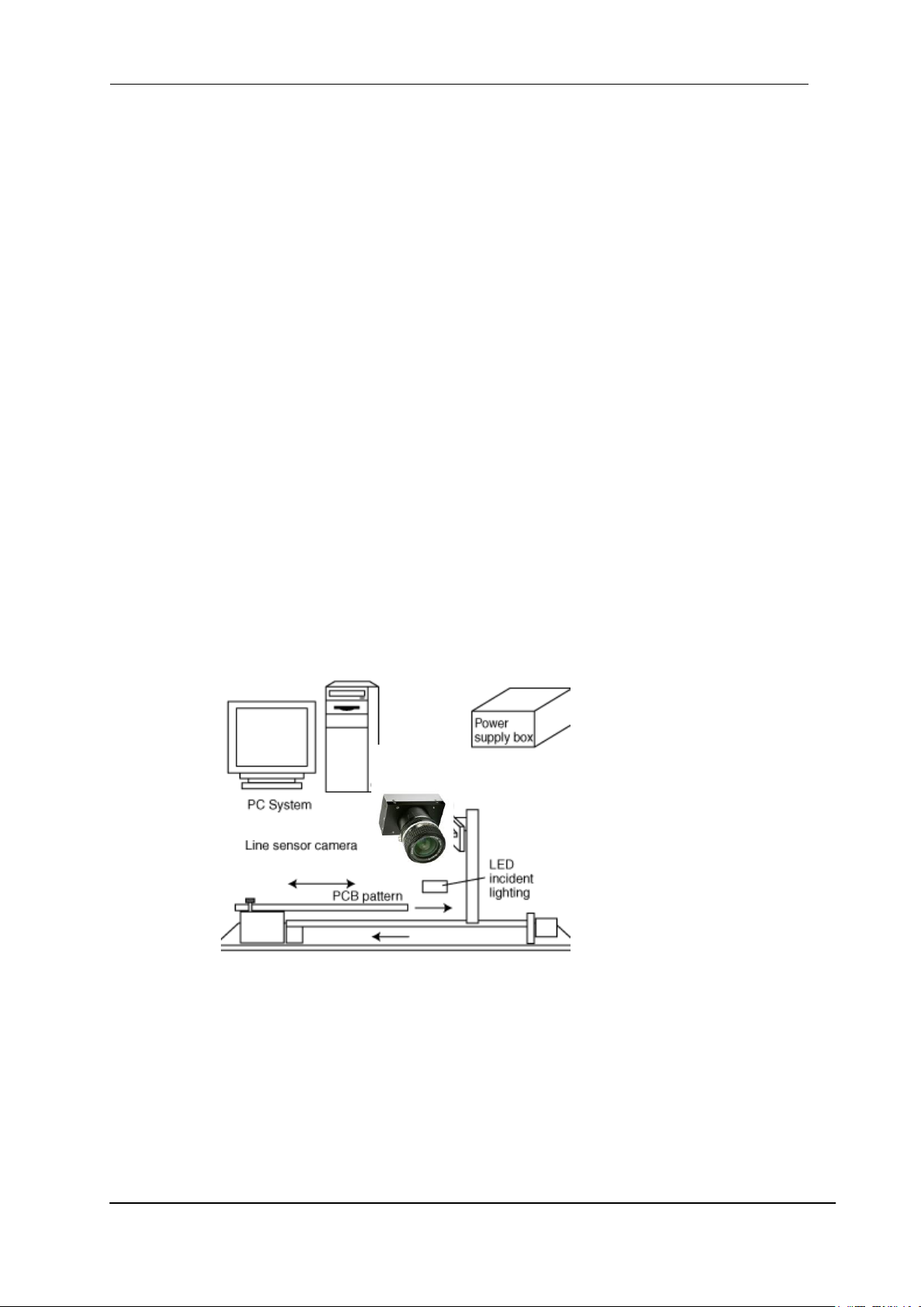
An example of Visual Inspection is shown below.
Figure 1-2-1 Visual Inspection of PCBs
Object of inspection (example) ・printed circuit boards
Device specification 1. Camera: Colour Line scan camera
2. Controller: Dedicated software for PC system
XCM4085TLCT6 UME-0062-01
Page 11
11 NED
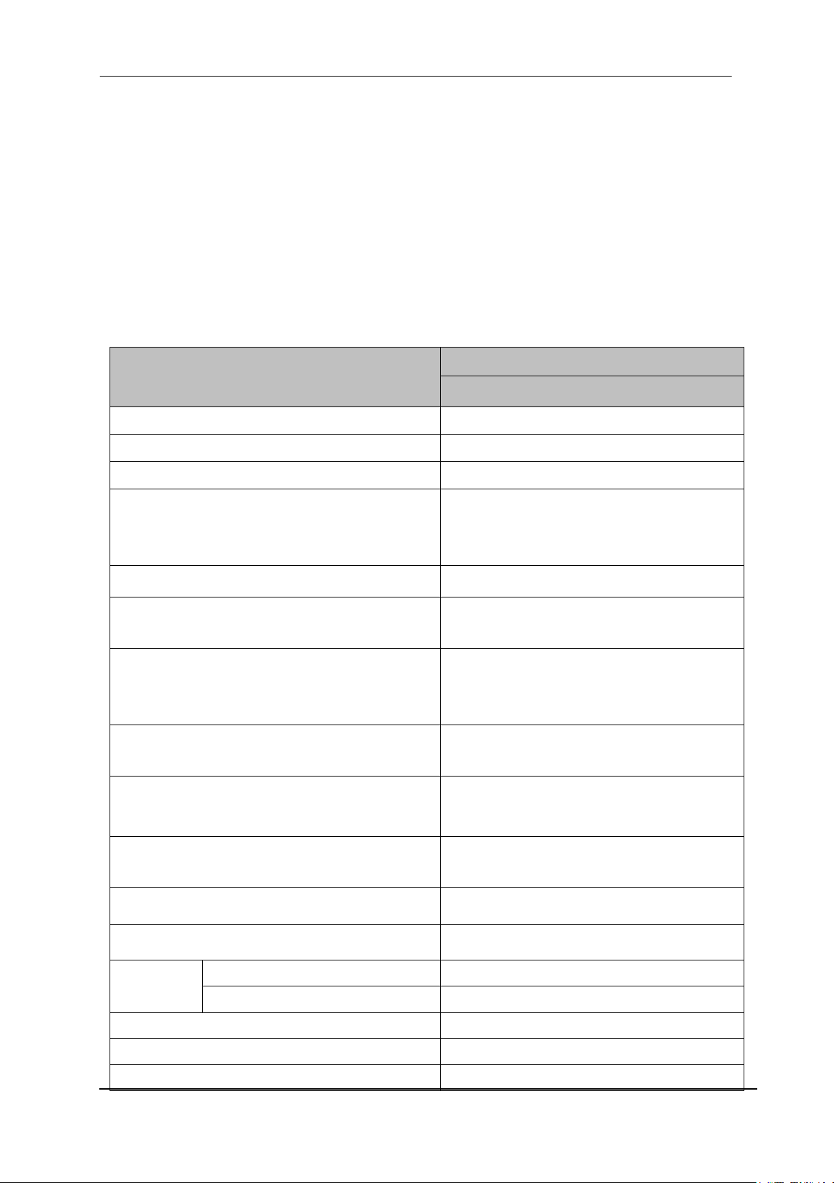
Items
Specifications
XCM4085TLCT6
Number of Pixels
4096x3 Lines
Pixel Size H x V (μm)
10x10
Sensor Length (mm)
40.96
Distance between two lines(μm)
*between G and R, between R and B
(Line positions from the top: G-R-B)
20 (equivalent to 2 lines width)
Data Rate (MHz)
170(each colour)
Min. Scan Period (μs) /
Max. Scan Rate [kHz]
25/[40]
* Data output 85MHz 2taps at each color
Saturation Exposure (lx・s) (typically)
[Minimum Gain, Pixel Correction Initial Value,
Daylight Fluorescent Light]
0.05*Visible Area (400~700nm)
Responsivity (V/ [lx・s]) (typically)
[Minimum Gain, Pixel Correction Initial Value, ]
100 *Visible Area (400~700nm)
*Analog 5V Conversion Sensitivity
Gain Adjustable Range
*Analog Amplifier +Digital (RGB Shared)
Analog Amplifier:x1 to x5.5 (6 Steps)
Digital :x1 to x2 (512 Steps)
Digital Offset Adjustable Range
(RGB shared)
-40 to 40 DN (161Steps): 8bit
-160 to 160 DN (161 Steps): 10bit
Video output Camera Link
Camera Link Medium/Base/Full
Configuration
Control Input
CC1: External Trigger Signal,
CC2-4: Not in use
Connectors
Data/Controller
3M: SDR26 [Mini Camera Link]
Power Supply
Hirose: HR10A (6Pin)
Lens Mount
Nikon F Mount
Operating Temperature (˚C)
0 to 50 *No Condensation
Power Supply Voltage (V)
DC 12 to 15 [+/-5%]
1.3 Image Sensor
The camera uses a CMOS sensor to acquire high quality images with high
sensitivity. The pixel size is 10μm x 10μm. The camera uses RGB with 4096 pixels
each.
1.4 Performance Specifications
The Performance Specifications are shown in Table 1-4-1. It shows the data when
the camera is operating at maximum scan rate, unless otherwise specified.
Table 1-4-1 Performance Specifications
XCM4085TLCT6 UME-0062-01
Page 12
12 NED
1.0
0
0.2
0.4
0.6
0.8
400 500 600 700
R
G
B
Consumption Current (mA) (typically)
800
Size W x H x D (mm)
62x100x72(F Mount)
Mass (g) (Camera only)
400(F Mount)
Additional Functions
1 Shading Correction
2 Gain/Offset/Video Output Adjustable
3 Programmable Exposure Control
4 Scan Direction Switching
5 Line delay function
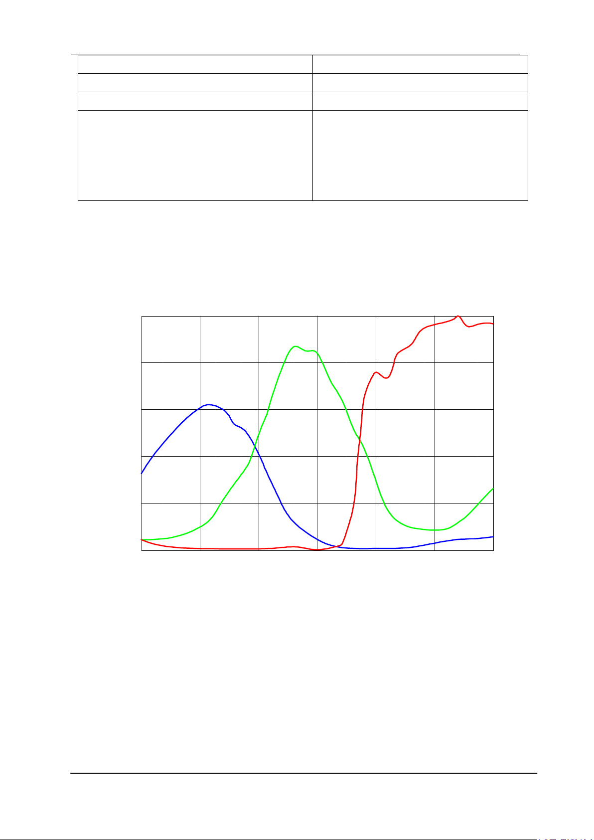
Figure 1-4-1 Spectral Responsivity
Relative Responsivity (%)
Note :
*1) DN : Digital Number (8bit : 0-255 / 10bit : 0-1023)
*2) Measurements were made at room temperature, daylight fluorescent light.
The spectral responsivity is shown below.
Wavelength (nm)
XCM4085TLCT6 UME-0062-01
Page 13
13 NED
1st Pixel
4-M4 Deep 6
2. Camera Setting and Optical Interface
2.1 Setting the Camera
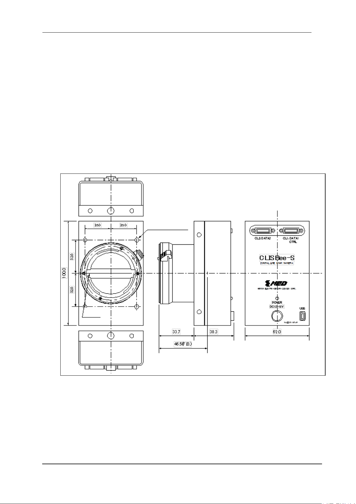
Use the M4 screw holes or the tripod screw hole to set the camera.
2.2 Fixing the Camera
Use the M4 screw holes (4 at the front) to set the camera.
The screw length for fixing the camera should be less than 6mm.
No X-, Y-axis orientation and tilt adjustment mechanism is available. Please
prepare an adjustment mechanism if required.
The dimensions of the camera are shown below.
XCM4085TLCT6 UME-0062-01
Unit: mm
Figure 2-2-1 Dimensions of the Camera (F Mount)
Page 14

14 NED
2.3 Optical Interface
Nikon F mount is provided as standard.
Notes:
1) The amount and wavelengths of light required to capture useful images depend
on the intended use. Factors include the physical properties, speed, the object’s
spectral characteristics, exposure time, the light source characteristics, the
specifications of the acquisition system and so on.
The exposure amount (exposure time x light amount) is the most important factor
in getting desirable images. Please determine the exposure amount after studying
what is most important to your system.
2) Keep these guidelines in mind when setting up your light source:
LED light sources are relatively inexpensive, provide a uniform field and longer life span
compared to other light sources. However, they also require a camera with excellent
sensitivity.
Halogen light sources generally provide very little blue light but have high infrared light
(IR) proportions.
Fiber-optic light distribution systems generally transmit very little blue light relative to IR.
Metal halide light sources are very bright but have a shorter life span compared to other
light sources.
3) Generally speaking, the brighter the light sources, the shorter the life span.
CMOS image sensors are sensitive to infrared (IR). We recommend using
daylight colour fluorescent lamps that have low IR emissions. If you use a halogen
light source, to prevent infrared from distorting the images use an IR cutoff filter
that does not transmit wavelengths.
XCM4085TLCT6 UME-0062-01
Page 15
15 NED
PC
Camera Link
Base or Medium or Full 対応
フレームグラバボード
カラーラインスキャンカメラ
XCM4085TLCT6
Camera Linkケーブル(SDR-MDR)
3M製 1MF26-L560-00C-xxx
電源ケーブル
DGPSH-10
カメラ用電源
DC+12V 30W
CL2
CL1
CL2
CL1
Colour Line Scan Camera
Camera Link Cable (SDR-MDR)
3M:1MF26-L560-00C-xxx
Camera Link
Base, Medium or Full
Configuration
Frame Grabber Board
Power Cable
Camera Power Supply
3. Hardware
3.1 Camera Connection
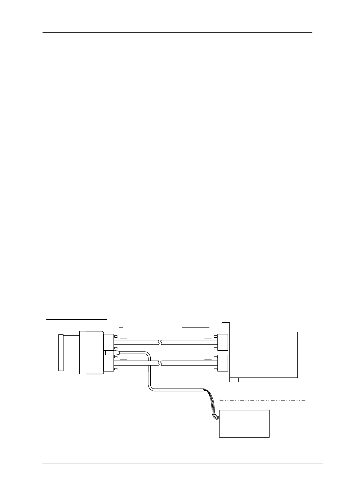
Use the camera in the following way:
① Camera Link cables must be used to connect the camera unit with the frame
grabber board.
Notes:
1) When using 2 taps at each colour or 10-bit, two Camera Link cables are
required. The cables should be of the same length and from the same
manufacturer.
2) When using 1 tap at each colour with 8-bit, one Camera Link cable is used.
Connect the cable to the CL1 connector (CL2 is unused).
3) Use asymmetric Camera Link cables and connect the camera with the
connector labeled as ”Camera side”.
4) A Medium and Full Configuration-compatible frame grabber has 2 connectors.
② Connect the camera with the designated power supply.
Notes:
Use the designated power cable to connect the camera with the power source for
the camera. Insert the plug end of the cable into the camera. Attach the opposite
end (loose wires) to the power unit. Other than those above, a personal
computer, a frame grabber board, a compatible lens, a lens mount, a light source
and an encoder are necessary, depending on the situation.
Check the specification of your frame grabber before connecting.
Figure 3-1-1 Connections between Camera and Frame Grabber Board and Power Supply
XCM4085TLCT6 UME-0062-01
Page 16
16 NED
Solios model
clock speed (MHz)
maximum cable length (m)
SOL 6M CL E*
(20~66MHz)
40
9.8
66
8.0
SOL 6M FC E*
(20~85MHz)
75
7.6
85
5.8
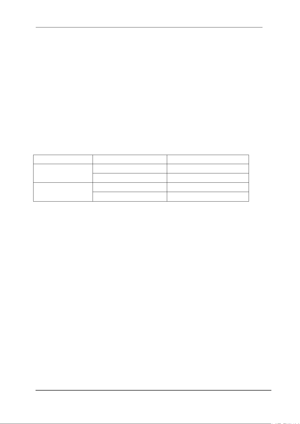
<Note: Choosing the appropriate Camera Link cable length >
According to the Camera Link Specification, the maximum cable length is 10m. But
the maximum cable length to be able to transfer data depends on the type of cable
performance and clock speed. The actual maximum transmission distance becomes
less than 10m at faster clock speeds, though the transmission distance of 10m is
feasible at slower clock speeds.
The following table shows values being calculated in accordance with the Camera
Link Specification 2007.Version1.2, using a typical cable (14B26-SZLB-xxx-0LC from
3M) and frame grabber board (Solios from Matrox). Please choose the appropriate
Camera Link cable type and length for your application. We recommend you perform
a connection test in advance.
Table 3-1-1 calculated value of maximum cable length
XCM4085TLCT6 UME-0062-01
Page 17
17 NED
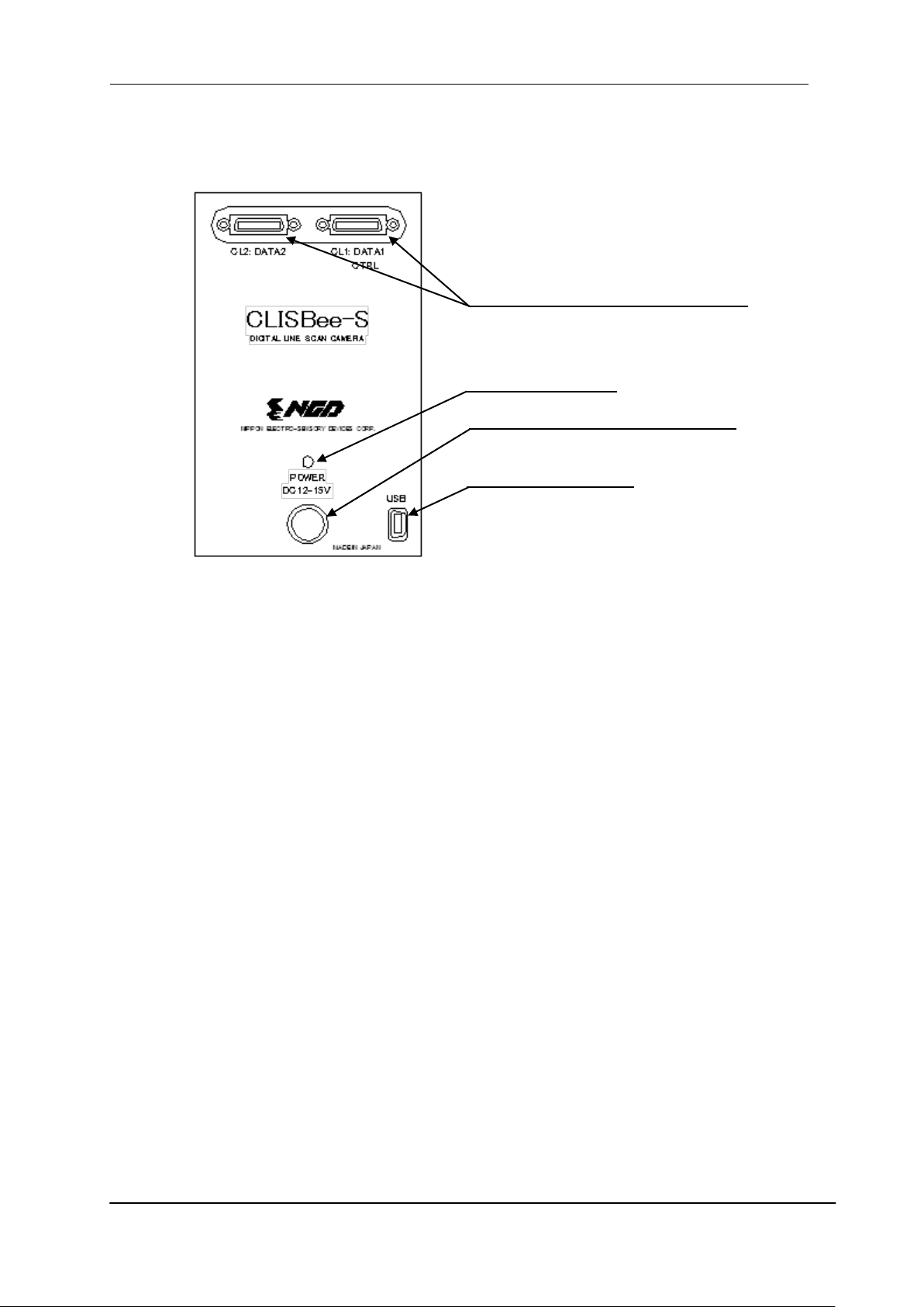
Power Connector(HIROSE HR10A 6P)
Indicator(Green)
Mini Camera Link Connector(SDR26)
Mini-USB Connector
※Used for maintenance.
3.2 Input / Output Connectors and Indicator
The layout of input /output connectors and the LED indicator are as follows.
Figure 3-2-1 Input / Output connectors and Power connector
XCM4085TLCT6 UME-0062-01
Page 18
18 NED
28 28
Frame Grabber BoardCamera
MDR26 Connector CL1
CC1(control input)
Cable
SerTC
SerTFG
CLK80MHz
Chanel Link Bus
LVAL,FVAL
DVAL,SP
Port A,B,C
CC2
CC3
CC4
X1±
X0±
X2±
X3±
XClk±
100Ω
100Ω
100Ω
100Ω
100Ω
100Ω
100Ω
100Ω
100Ω
100Ω
100Ω
SerTFG±
SerTC±
CC1±
CC2±
CC3±
CC4±
MDR26 Connector
X1±
X0±
X2±
X3±
XClk±
SerTFG±
SerTC±
CC1±
CC2±
CC3±
CC4±
LVDS_DRIVER(NS)
DS90CR287MTD
equivalent
LVDS_DRIVER/
RECIVER(NS)
DS90LV019TM
equivalent
LVDS_RECIVER(NS)
DS90LV048AT
equivalent
LVDS_RECIVER(NS)
DS90CR288AMTD
recommended
LVDS_DRIVER/
RECIVER(NS)
DS90LV019TM
recommended
LVDS_DRIVER(NS)
DS90LV047AT
recommended
28 28
MDR 26 Connector CL2
Cable
CLK80MHz
Chanel Link Bus
LVAL,FVAL
DVAL,SP
Port D,E,F
Y1±
Y0±
Y2±
Y3±
YClk±
100Ω
100Ω
100Ω
100Ω
100Ω
MDR 26 Connector
Y1±
Y0±
Y2±
Y3±
YClk±
LVDS_DRIVER(NS)
DS90CR287MTD
equivalent
LVDS_RECIVER(NS)
DS90CR288AMTD
recommended
28 28
CLK80MHz
Chanel Link Bus
LVAL,FVAL
DVAL,SP
Port G,H
Z1±
Z0±
Z2±
Z3±
ZClk±
100Ω
100Ω
100Ω
100Ω
100Ω
Z1±
Z0±
Z2±
Z3±
ZClk±
LVDS_DRIVER(NS)
DS90CR287MTD
equivalent
LVDS_RECIVER(NS)
DS90CR288AMTD
recommended
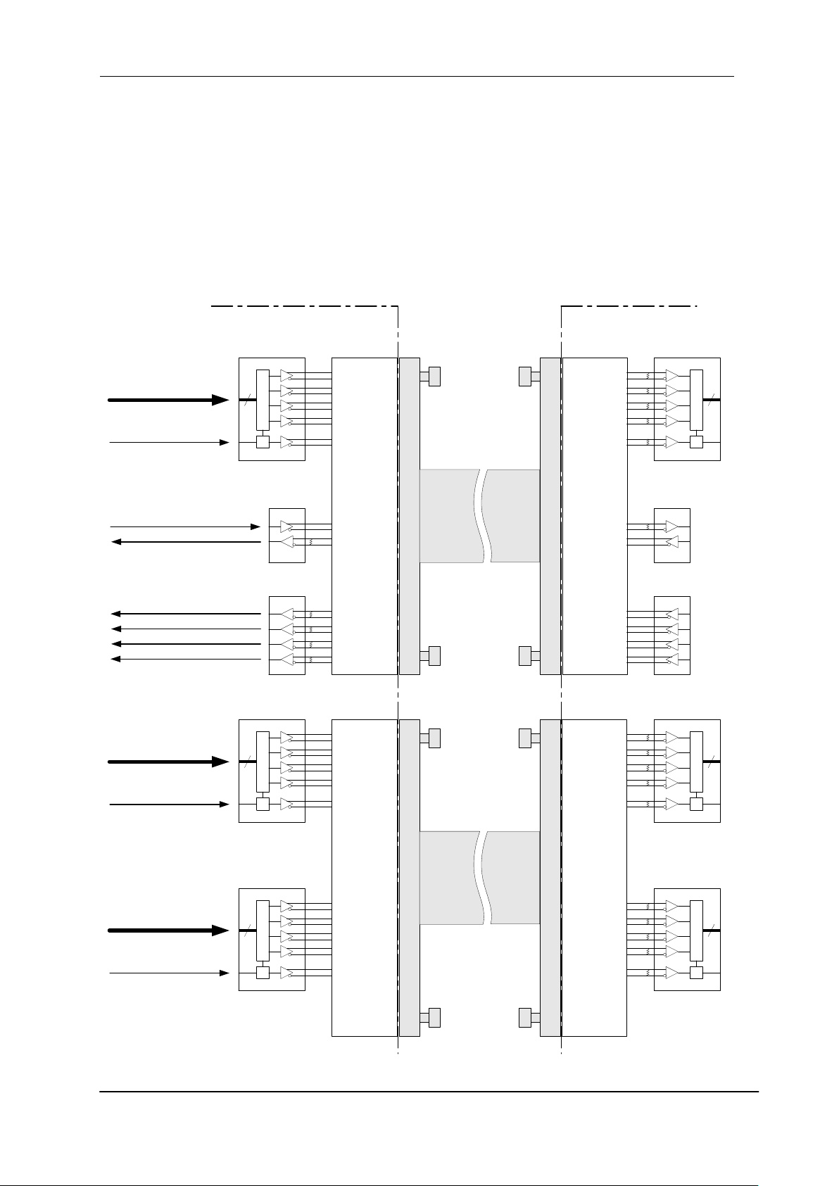
3.3 Connectors・Pin Assignments・Cables
This camera adopts Configurations of Camera Link interface standards.
-Base Configuration for output of 1 tap at each colour with 8 bits,
-Medium Configuration for output of 2 taps at each colour with 8 bits, output of 2 taps at
each colour or output 1 tap at each colour with 10 bits
-Full Configuration for output of 2 taps at each colour with 10bits
Figure 3-3-1 shows the interface for the camera and a typical implementation for
the frame grabber interface. (Example of Medium Configuration)
Figure 3-3-1 Camera / Frame Grabber Interface
XCM4085TLCT6 UME-0062-01
Page 19
19 NED
8bit RGB o/e
10bit RGB o/e
8bit RGB o/e
10bit RGB o/e
Medium
Configuration
Full
Configuration
Medium
Configuration
Full
Configuration
Port A0
Ro0
Ro0
Port E0
Ge0
Bo0
Port A1
Ro1
Ro1
Port E1
Ge1
Bo1
Port A2
Ro2
Ro2
Port E2
Ge2
Bo2
Port A3
Ro3
Ro3
Port E3
Ge3
Bo3
Port A4
Ro4
Ro4
Port E4
Ge4
Bo4
Port A5
Ro5
Ro5
Port E5
Ge5
Bo5
Port A6
Ro6
Ro6
Port E6
Ge6
Bo6
Port A7
Ro7
Ro7
Port E7
Ge7
Bo7
Port B0
Go0
Ro8
Port F0
Be0
Bo8
Port B1
Go1
Ro9
Port F1
Be1
Bo9
Port B2
Go2
-
Port F2
Be2
Be1
Port B3
Go3
-
Port F3
Be3
Be0
Port B4
Go4
Go8
Port F4
Be4
Re8
Port B5
Go5
Go9
Port F5
Be5
Re9
Port B6
Go6
-
Port F6
Be6
Be8
Port B7
Go7
-
Port F7
Be7
Be9
Port C0
Bo0
Go0
Port G0 - Ge0
Port C1
Bo1
Go1
Port G1 - Ge1
Port C2
Bo2
Go2
Port G2 - Ge2
Port C3
Bo3
Go3
Port G3 - Ge3
Port C4
Bo4
Go4
Port G4 - Ge4
Port C5
Bo5
Go5
Port G5 - Ge5
Port C6
Bo6
Go6
Port G6 - Ge6
Port C7
Bo7
Go7
Port G7 - Ge7
Port D0
Re0
Re0
Port H0 - Ge8
Port D1
Re1
Re1
Port H1 - Ge9
Port D2
Re2
Re2
Port H2 - Be2
Port D3
Re3
Re3
Port H3 - Be3
Port D4
Re4
Re4
Port H4 - Be4
Port D5
Re5
Re5
Port H5 - Be5
Port D6
Re6
Re6
Port H6 - Be6
Port D7
Re7
Re7
Port H7 - Be7
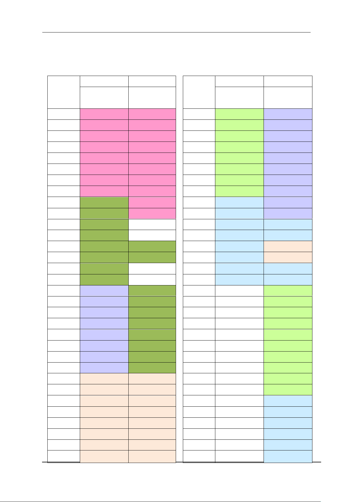
The camera link port assignment is shown in the table below in case of output of 2 taps at
each colour with 8 bits and output of 2 taps at each colour with 10 bits.
Table 3-3-1 Port Assignment of Output
XCM4085TLCT6 UME-0062-01
Page 20
20 NED
1142153
16
1124122513
26
M2x0.4
100Ω
(DRIVER)
(RECEIVER)
H or L
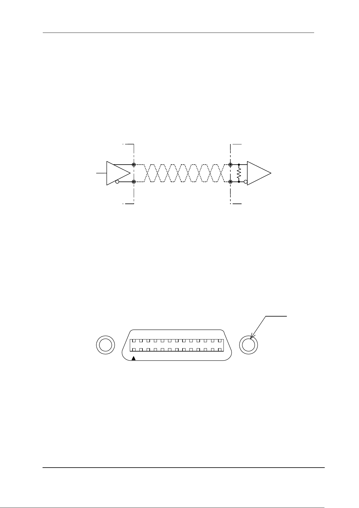
Notes:
1) In 24-bit colour, Base Configuration is used, so it is not necessary to connect a
cable to CL2.
2) Do not make the driver side of LVDS open but set the logic to H or L, even if not
used.
3) Set the LVDS, Channel Link receiver side to 100-ohm termination.
Figure 3-3-2 Circuit of LVDS
The camera has 26-pin SDR connectors for control signals of Camera Link, data
signals and serial communications.
Figure 3-3-3 Camera Link Connector
XCM4085TLCT6 UME-0062-01
Page 21
21 NED
No
NAME
No
NAME
I/O No
NAME
No
NAME
I/O 1 Inner Shield
14
Inner Shield
- 1 Inner Shield
14
Inner Shield
- 2 X0 -
15
X0 +
OUT
2
Y0 -
15
Y0 +
OUT
3
X1 -
16
X1 +
OUT
3
Y1 -
16
Y1 +
OUT
4
X2 -
17
X2 +
OUT
4
Y2 -
17
Y2 +
OUT
5
Xclk -
18
Xclk+
OUT
5
Yclk -
18
Yclk +
OUT
6
X3 -
19
X3 +
OUT
6
Y3 -
19
Y3 +
OUT
7
SerTC +
20
SerTC -
IN 7 100Ωterminated
20
100Ωterminated
- 8 SerTFG -
21
SerTFG +
OUT
8
Z0 -
21
Z0 +
OUT
9
CC1 -
22
CC1 +
IN 9 Z1 -
22
Z1 +
OUT
10
CC2 +
23
CC2 -
IN
10
Z2 -
23
Z2 +
OUT
11
CC3 -
24
CC3 +
IN
11
Zclk -
24
Zclk +
OUT
12
CC4 +
25
CC4 -
IN
12
Z3 -
25
Z3 +
OUT
13
Inner Shield
26
Inner Shield
-
13
Inner Shield
26
Inner Shield
-
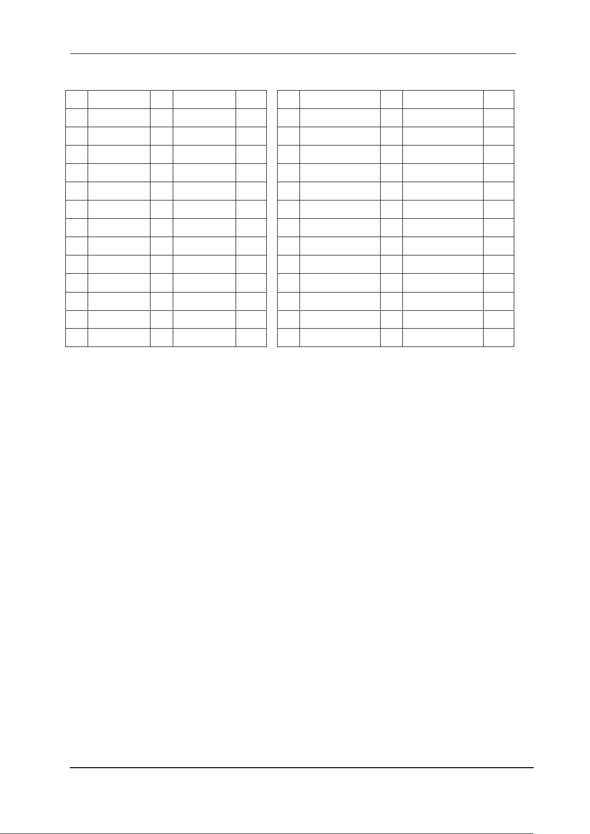
Table 3-3-1 Camera Link Connector (26-pin SDR Connector) pin assignments
CL1(Base/Medium Configuration) CL2(Medium/Full Configuration)
Explanation of Signals
Inner Shield: Shield cable (GND)
X0+, X0-…X3+, X3-: Data output (Channel Link)
Xclk+, Xclk-: Clock output for above data output synchronization
(Channel Link)
Y0+,Y0-・・・Y3+,Y3-: Data output (Channel Link)
Yclk+,Yclk-: Clock output for above data output synchronization
(Channel Link)
Z0+,Z0-・・・Z3+,Z3-:Data output (Channel Link)
Zclk+,Zclk -:Clock output for above data output synchronization (Channel Link)
SerTC+, SerTC- : Serial data input (LVDS)
SerTFG+, SerTFG-: Serial data output (LVDS)
CC1+, CC1- : External synchronous signal input (LVDS)
CC2+, CC2-, CC3+, CC3-, CC4+, CC4-: Not in use (LVDS)
Camera Link compatible cable
XCM4085TLCT6 UME-0062-01
3M: 1MF26-L560-00C-xxx by or equivalent
Notes:
1) To avoid uncoupling of the cable connectors during power on, make sure to
clamp them with the locking screws.
2) Do not unplug the cables while power is being supplied to the camera.
Page 22
22 NED
1
2
3
6
5
4
No
NAME
Colour of Cable
1
DC12 –15V
White
2
DC12 –15V
Red
3
DC12 –15V
-
4
GND
Green
5
GND
Black
6
GND
-
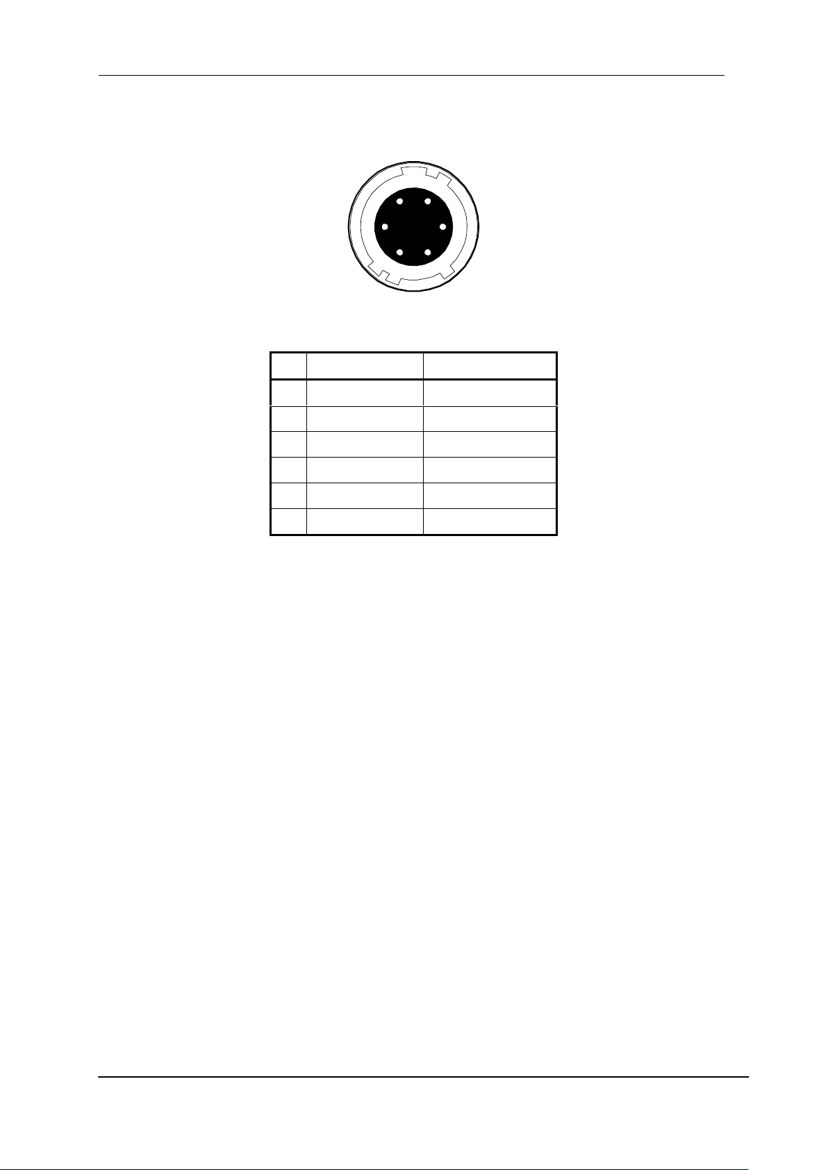
This camera uses 6-pin round shape push-pull lock type connector for the Power
Supply
Figure 3-3-4 Power Supply Connector (HIROSE: HR10G-7R-6PB)
Table 3-3-2 Pin Assignment of Power Supply Connector
Note: The cable colour in the table describes the compatible cable DGPSH-10.
3.4 Power Supply
The camera requires a single power supply (DC+12 to +15V).
The indicator (LED green) blinks when power is supplied. After a short period, it
changes to a constant light, indicating that the camera is operational.
Notes:
1) When selecting a power source, choose one with the capacity to allow for
inrush current. (30 W or more recommended)
2) Insert the cable plug securely until it locks into position. This is to prevent the
connector from coming loose during power transmission.
3) If the lamp fails to illuminate even after power is switched on, turn OFF power
immediately. Inspect wiring. Check the voltage and capacity of the supplied
power source.
4) It is recommended that the shield processing of the power cable to be
connected with GND on the power supply side.
Compatible Cable (Compatible plug): DGPSH10 (HIROSE:HR10A-7P –6S)
Power supply voltage: DC+12 –15V (+/-5%)
Consumption Current (rated): DC+12V: 800mA
XCM4085TLCT6 UME-0062-01
Page 23

23 NED
4 Camera Control
The camera can be controlled through the serial communication. Two methods
can be used to change the camera’s parameters. The first approach is to change
parameters using CLISBeeCtrl (Camera control software). (See “8 CLISBeeCtrl”.)
Or you can also change the parameters directly from your application by using
serial communication commands to set values in the camera register.
Once the camera has been set up according to your requirements, the camera
can be used to read data without need of controlling it via the serial interface.
4.1 Flow of Camera Control
4.1.1 Command Overview
The serial interface uses a simple ASCII-based command.
Communication begins when the computer sends control commands to the
camera.
The camera receives and interprets the computer commands and then
executes control operations accordingly.
Transmission ends when the camera returns the analyzed results of the
control commands to the computer.
Always allow the previous transmission to end before starting the next
transmission. (Only one command can be sent per transmission.)
4.1.2 Camera Receiving Message (PC Sending Command)
Format S1 CMD CR
Format S2 CMD □ VAL 1 CR
Format S3 CMD □ VAL 1 □ VAL2 CR
CMD: Control text (3 Bytes) Use 3~5 lowercase letters only. No numerals allowed.
CR: Carriage Return (0x0D)
□: Space (0x20) or Comma (0x2C)
VAL1: Setting value (decimal), numerical values only
VAL2: Setting value (decimal), numerical values only
XCM4085TLCT6 UME-0062-01
Page 24
24 NED
Camera Response
Meaning
OK
Camera executed command
CMD ERR!
Command is not valid
CMD OVR ERR!
Command text line is too long
When the control character exceeds 254 characters
CMD FAIL!
When trying to perform acquisition of pixel correction data, but
pixel correction mode is set to any mode other than User
Setting.
VAL ERR!
Parameter accepted was outside of specified
MEM ERR!
Camera memory error
TRG ERR!
When the scanning interval becomes more than a few seconds
when arbitrary pixel correction data is acquired.
ADJ ERR!
When automatic white balance cannot be performed
4.1.3 Camera Sending Message (PC Receiving Message)
Format R 1 >R CR >[SB] CR EOT
Format R 2 >R CR >[MEM] CR >[SB] CR EOT
> : Results start text (0 x 3E)
R: Camera receive command analyzed results (See table 4-1-3-1)
[SB] : Camera receive command send back
[MEM] : Memory data readout value
CR: Separated text (0 x 0D)
EOT: Send command all text end text (0 x 04)
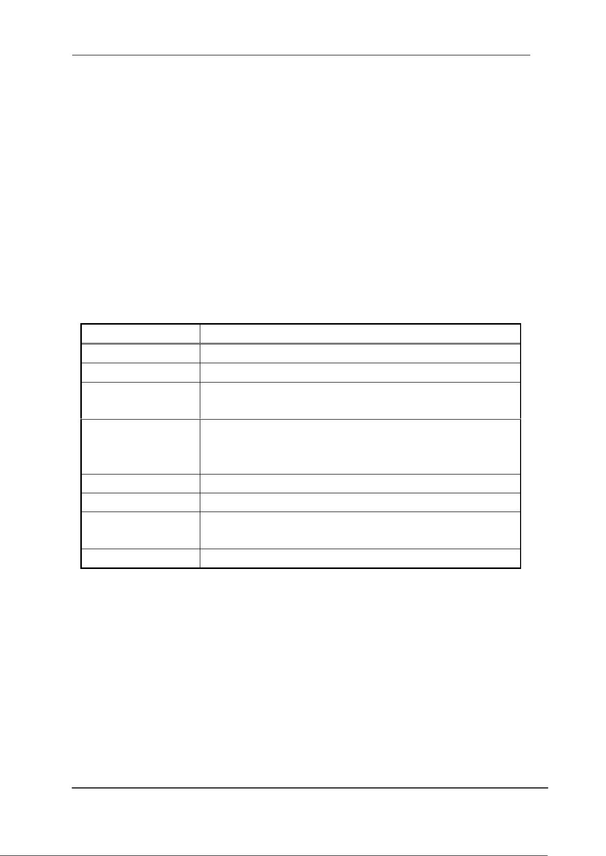
Table 4-1-3-1 Error Messages
XCM4085TLCT6 UME-0062-01
Page 25
25 NED
Control Item
CMD
VAL1
VAL2
Control Description
Analog Gain
(RGB Shared)
gax
0 to 5
x1,x1.5,x2,x3,x4,x5.5
(x1-x3 recommended)
Digital Gain (RGB
Shared)
gdx
0 to 511
x1… x2 (1+VAL1/511)
Digital Gain R
gdxr
0 to 1022
x1~x3 (1+VAL1/511)
Digital Gain G
gdxg
0 to 1022
x1~x3 (1+VAL1/511)
Digital Gain B
gdxb
0 to 1022
x1~x3 (1+VAL1/511)
Auto white balance
Setting
awb
Run gdxr,gdxg,gdxb auto balance
function
Auto white balance reset
rwb
Set gdxr,gdxg,gdxb to x1
Digital Offset (RGB
Shared)
odx
-80 to 80
-40~+40DN(0.5DN/step at 8bit)
-160~+160DN(2.0DN/step at 10bit)
Digital Offset R
odxr
-40 to 40
-20~+ 20DN(0.5DN/step at 8bit)
-80~+80DN(2.0DN/step at 10bit)
Digital Offset G
odxrg
-40 to 40
- 20~+ 20DN(0.5DN/step at 8bit)
-80~+80DN(2.0DN/step at 10bit)
Digital Offset B
odxb
-40 to 40
- 20~+ 20DN(0.5DN/step at 8bit)
-80~+80DN(2.0DN/step at 10bit)
Exposure Mode
inm
0 /1/2
Free Run / Ext Edge / Ext Level
Programmable Exposure
Time
int
64
31 to
32767
22.12~23373.17 μs
*See 4.8 for more information
Data Output Clock
clkcl
85/40
85MHz/40MHz
Output Tap Setting
tap
1/2
Number of taps at each RGB for output
Output Bit Setting
dep
8/10
Number of bits at each RGB for output
Line Delay Setting
ldly
-8~8
Numbers of delay lines between output
datas at each RGB
Line Fine Adjusting
Correction
ldlys
-5~5
Line fine adjusting correction for output
datas at each RGB
Test Pattern
tpn
0/1/2
Off/Gray/Gray XY/Color Bar
Pixel Correction Setting
shc
0/1/2/3
0:Correction Off
1:Factory correction On
2:User arbitrary correction 1 On
3:User arbitrary correction 2 On
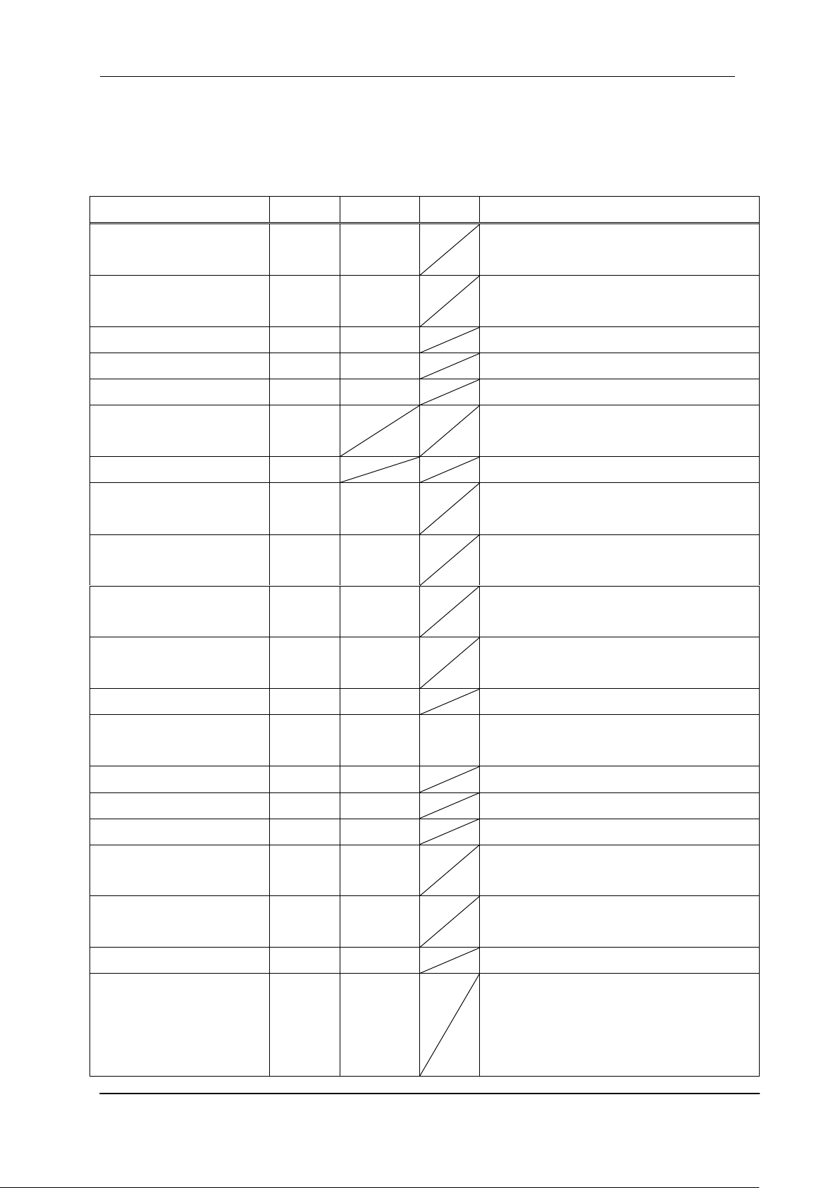
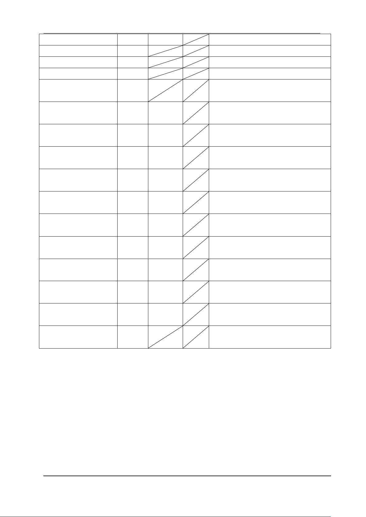
4.1.4 Camera Control Commands
Table 4-1-4-1 shows the list of Camera Control Commands.
Table 4-1-4-1 Lists of Camera Control Commands
XCM4085TLCT6 UME-0062-01
Page 26
26 NED
Scanning Direction
rev
0 /1
0: Forward / 1: Reverse
Memory Initializing
rst
Reset to factory settings
Memory Load
rfd
Readout setup data in memory
Memory Save
sav
Store present setup data in memory
Pixel Correction Data
Save [gray]
wht
Arbitrary user’s correction data is
acquired and stored in the memory.
Pixel Correction target
value (factory settings) R
MFr
0 to 1023
Factory correction data
R target value(10bit DN)
Pixel Correction target
value (factory settings) G
MFg
0 to 1023
Factory correction data
G target value(10bit DN)
Pixel Correction target
value (factory settings) B
MFb
0 to 1023
Factory correction data
B target value(10bit DN)
Pixel Correction target
value (user settings 1) R
MUr
0 to 1023
User arbitrary correction data 1
R target value(10bit DN)
Pixel Correction target
value (user settings 1) G
MUg
0 to 1023
User arbitrary correction data 1
G target value(10bit DN)
Pixel Correction target
value (user settings 1) B
MUb
0 to 1023
User arbitrary correction data 1
B target value(10bit DN)
Pixel Correction target
value (user settings 2) R
MVr
0 to 1023
User arbitrary correction data 2
R target value(10bit DN)
Pixel Correction target
value (user settings 2) G
MVg
0 to 1023
User arbitrary correction data 2
G target value(10bit DN)
Pixel Correction target
value (user settings 2) B
MVb
0 to 1023
User arbitrary correction data 2
B target value(10bit DN)
Gamma Correction
setting
gamma
0/1/2/3
Off(1.0)/0.45/0.56/Negative-Positive
Operation Status
Readout
sta
Readout the current camera settings
XCM4085TLCT6 UME-0062-01
Page 27
27 NED
Control Item
CMD
VAL1
VAL2
Control Description
Analog Gain
gax 0
x1 (0 dB)
Digital Gain (RGB Shared)
gdx 0
x1 (0 dB)
Digital Gain R
gdxr 0
x1 (0 dB)
Digital Gain G
gdxg 0
x1 (0 dB)
Digital Gain B
gdxb 0
x1 (0 dB)
Digital Offset (RGB Shared)
odx 0
±0DN
Digital Offset R
odxr 0
±0DN
Digital Offset G
odxg 0
±0DN
Digital Offset B
odxb 0
±0DN
Exposure Mode
inm 0
Free Run
Programmable Exposure Time
int
64
200
142.7μs
Data Output Clock
clkcl
85
85MHz
Output Tap Setting
tap 2
2 taps at each RGB for output
Output Bit Setting
dep 8
8 bits at each RGB for output
Line Delay Setting
ldly
2
2 delay lines between output
datas at each RGB
Line Fine Adjusting
Correction
ldlys
0
No fine adjusting correction for
output line at each RGB
Test Pattern
tpn 0
Off
Pixel Correction Setting
shc 1
Factory correction data On,
(Daylight Fluorescent Light)
Scanning Direction
rev 0
Forward
Pixel Correction target value
(factory settings) R
MFr
768
Factory correction data
R target value(768 DN)
Pixel Correction target value
(factory settings) G
MFg
768
Factory correction data
G target value(768 DN)
Pixel Correction target value
(factory settings) B
MFb
768
Factory correction data
B target value(768 DN)
Pixel Correction target value
(user settings 1) R
MUr
768
User arbitrary correction data 1
R target value(768 DN)
Pixel Correction target value
(user settings 1) G
MUg
768
User arbitrary correction data 1
G target value(768 DN)
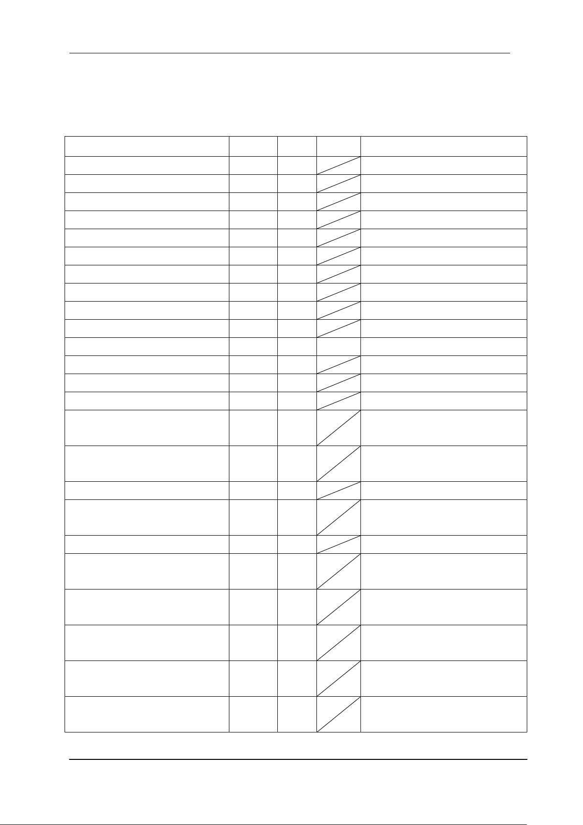
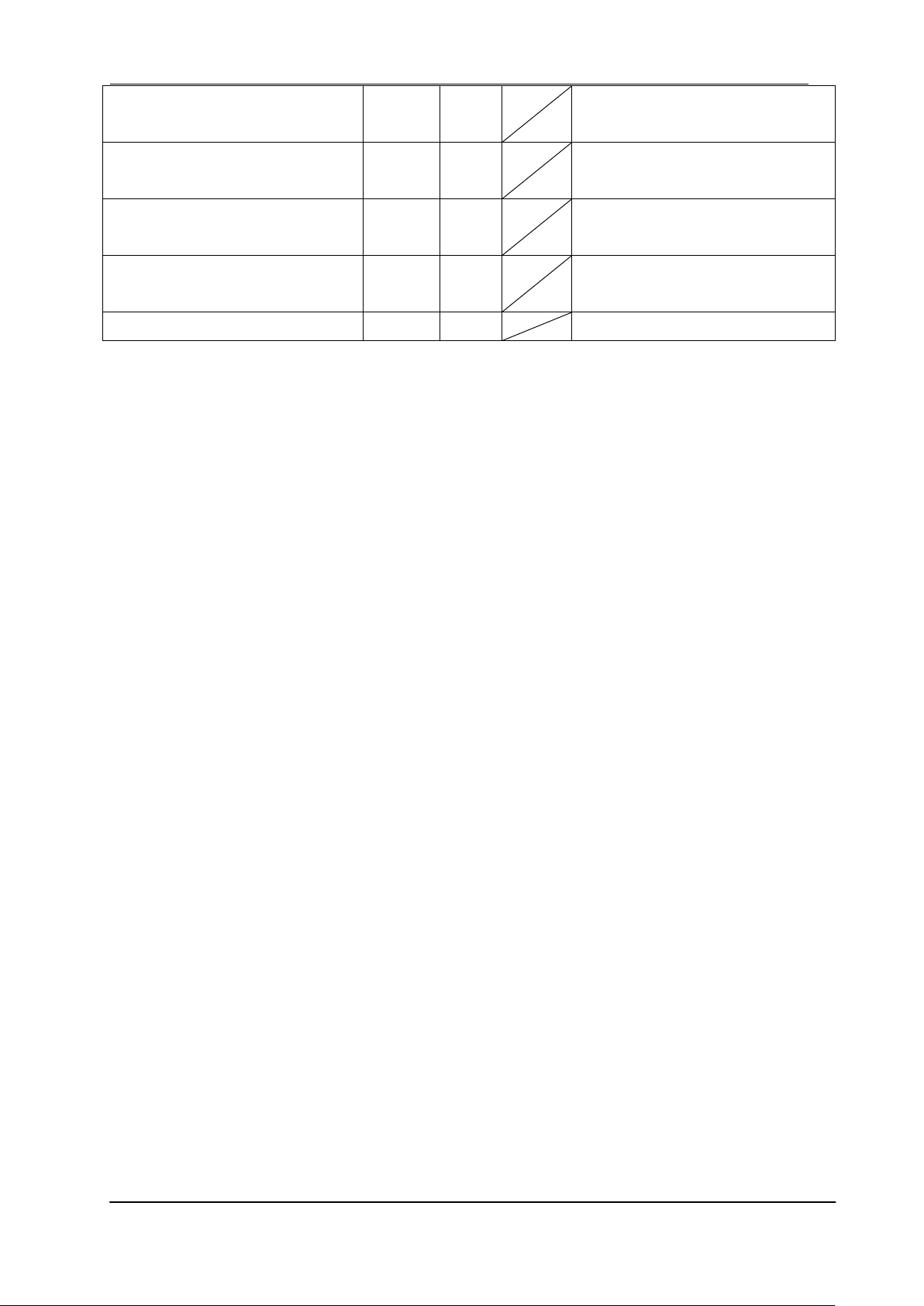
4.1.5 Memory Setup Values (Factory Settings)
The memory setup values (factory settings) are shown in Table 4-1-5-1.
Table 4-1-5-1 Memory Setup Values (Factory Settings)
XCM4085TLCT6 UME-0062-01
Page 28
28 NED
Pixel Correction target value
(user settings 1) B
MUb
768
User arbitrary correction data 1
B target value(768 DN)
Pixel Correction target value
(user settings 2) R
MVr
768
User arbitrary correction data 2
R target value(768 DN)
Pixel Correction target value
(user settings 2) G
MVg
768
User arbitrary correction data 2
G target value(768 DN)
Pixel Correction target value
(user settings 2) B
MVb
768
User arbitrary correction data 2
B target value(768 DN)
Gamma Correction Setting
gamma
0
Off (1.0)
4.2 Details on Commands
4.2.1 Setting Analog Gain
Sets analog gain in 6 steps between x 1 to x 5.5.
Format S2 CMD □ VAL1 CR Format R1 >R CR >[SB] CR EOT
CMD gax
VAL 0 (x1) to 5 (x5.5)
<Example>
Send: gax □ 2 CR (Setting analog gain 2(x2))
Receive: >OK CR>gax □ 2 CR EOT
4.2.2 Setting Digital Gain (1)
Sets the camera digital gain.
RGB Shared (gdx): Sets digital gain in 512 steps between x1 and x2.
R, G, B individual (gdxr, gdxg, gdxb): Sets digital gain in 1023 steps between x1 and
x3.
Format S2 CMD □ VAL1 CR, Format R1 >R CR >[SB] CR EOT
CMD gdx, gdxr, gdxg, gdxb
VAL Shared:0 (x 1) to 511 (x 2) R,G,B individual: 0 (×1)~ 1022(×3)
<Example>
Send:gdxb □ 256 CR (Setting digital gain B 256 (1+256/511) =x1. 50))
XCM4085TLCT6 UME-0062-01
Receive::>OK CR > gdxb □ 256 CR EOT
Page 29

29 NED
4.2.3 Setting Digital Gain (2)
Set individual R, G, B gain (gdxr, gdxg, gdxb), “automatically”.
Format S1 CMD CR Format R2 >R CR >[MEM] CR >[SB] CR EOT
CMD awb
<Example>
Send:awb CR
Receive::>OK CR > awb CR EOT
4.2.4 Setting Digital Gain (3)
Set R,G,B individual digital gain settings (gdxr, gdxg, gdxb) to initial value of “0”
Format S1 CMD CR Format R2 >R CR >[MEM] CR >[SB] CR EOT
CMD rwb
<Example>
Send:rwb CR
Receive::>OK CR > rwb CR EOT
4.2.5 Setting Digital Offset
Sets digital offset -60 to 60(0.5DN/step at 8bit), -240 to 240(2.0DN/step at 10bit)
Format S2 CMD □ VAL1 CR, Format R1 >R CR >[SB] CR EOT
CMD odx,odxr, odxg, odxb
VAL -80 to 80 (odx) ,-40 to 40(odxr, odxg, odxb)
<Example>
Send:odxg □ 5 CR (Sets Digital Offset G to +10DN at 10bit)
Receive::>OK CR >odxg □ 5 CR EOT
4.2.6 Setting Exposure Mode
Sets the exposure mode.
Format S2 CMD □ VAL1 CR , Format R1 >R CR >[SB] CR EOT
CMD inm
VAL 0,1,2
<Example>
Send:inm □ 0 CR (Sets the exposure mode to free run)
Receive::>OK CR >inm □ 0 CR EOT
XCM4085TLCT6 UME-0062-01
Page 30

30 NED
4.2.7 Setting Exposure Time
Sets the exposure time. Only operates at Free Run/Ext Edge.
Format S3 CMD □ VAL1 □ VAL2 CR, Format R1 >R CR >[SB] CR EOT
CMD int
VAL1 64 (Fixed Dividing setting)
VAL2 *31~32767 (Setting Counter value)
Note: *The ranges of these counter values vary according to Output data
formats as follows.
31~32767 (at 85MHz 2taps )
65~32767(at 85MHz 1tap)
70~32767(at 40MHz 2taps)
141~32767(at 40MHz 1tap)
<Example>
Send:int □ 64 □ 140 CR (Setting exposure time 100μs)
Receive::>OK CR >int □ 64 □ 140 CR EOT
Note:
See 4.8.1.1 for the calculation of the exposure time.
4.2.8 Setting Data Output Clock Frequency
Sets the clock frequency of the camera data output.
Format S3 CMD □ VAL1 CR , Format R1 >R CR >[SB] CR EOT
CMD clkcl
VAL1 85,40(85:85MHz,40:40MHz)
<Example> Clock Frequency of Data output, 40MHz
Send:clkcl □ 40 □ CR
Receive::>OK CR >clkcl □ 40 □ CR EOT
4.2.9 Setting Data Output Tap Number
Sets the tap numbers of the camera data output.
Format S3 CMD □ VAL1 CR , Format R1 >R CR >[SB] CR EOT
CMD tap
VAL1 1,2(1:1 tap at each RGB、2:2 taps at each RGB)
<Example> Tap numbers of the data output, 1
Send:tap □ 1 □ CR
Receive::>OK CR >tap □ 1 □ CR EOT
XCM4085TLCT6 UME-0062-01
Page 31

31 NED
4.2.10 Setting Data Output Bit Number
Sets the bit numbers of the data output.
Format S3 CMD □ VAL1 CR , Format R1 >R CR >[SB] CR EOT
CMD dep
VAL1 8,10(8: 8bits output at each RGB, 10: 10bits output at each RGB)
<Example> Bit numbers of the data output, 10bit
Send:dep □ 10 □ CR
Receive::>OK CR >dep □ 10 □ CR EOT
4.2.11 Setting Delay Line Number
Sets the delay line numbers between the output datas at each RGB
Format S3 CMD □ VAL1 CR , Format R1 >R CR >[SB] CR EOT
CMD ldly
VAL1 -8~8(delay line numbers between the datas at each RGB)
<Example> Reverse movement direction, 1:1 of reduced scale ratio of length
and width at image acquisition
Send:ldly □ -2 □ CR
Receive::>OK CR >ldly □ -2 □ CR EOT
4.2.12 Setting Line Fine Adjusting Correction Between Output Datas
Sets the line fine adjusting correction between the output datas at each RGB
Format S3 CMD □ VAL1 CR , Format R1 >R CR >[SB] CR EOT
CMD ldlys
VAL1 -5~5(line fine adjusting correction value between the output datas
at each RGB)
<Example> 0.5 line correction in the movement direction
Send:ldlys □ 5 □ CR
Receive::>OK CR >ldlys □ 5 □ CR EOT
4.2.13 Setting Scanning Direction
Switch scanning direction.
Format S2 CMD □ VAL1 CR, Format R1 >R CR >[SB] CR EOT
CMD rev
VAL1 0,1 (0:Forward, 1:Reverse)
<Example>
Send:rev □ 1 CR (Reverse output)
Receive::>OK CR >rev □ 1 CR EOT
XCM4085TLCT6 UME-0062-01
Page 32

32 NED
4.2.14 Saving Pixel Correction Data
Acquires the current pixel correction data (gray) and saves it in the flash memory.
One set of correction data can be saved for each step of analog gain.
Format S1 CMD CR, Format R1 >R CR >[SB] CR EOT
CMD wht
<Example>
Send:wht CR
Receive::>OK CR >wht CR EOT
4.2.15 Setting Pixel Correction (1)
Switches between pixel correction data settings.
Format S2 CMD □ VAL1 CR, Format R1 >R CR >[SB] CR EOT
CMD shc
VAL1 0,1,2,3 (0:Correction Off
1: Factory correction data On
2: User arbitrary correction data 1 On
3: User arbitrary correction data 2 On)
<Example>
Send:shc □ 2 CR (User arbitrary correction data 1)
Receive::>OK CR >shc □ 2 CR EOT
4.2.16 Setting Pixel Correction (2)
Manually sets the pixel correction target value.
Format S2 CMD □ VAL1 CR, Format R1 >R CR >[SB] CR EOT
CMD MFr、MFg、MFb、MUr、MUg、MUb、MVr、MVg、MVb
VAL1 0~1023
<Example>Sets the Blue target value to 900DN while using User arbitrary correction
data 1
Send:MUb □ 900 CR
Receive::>OK CR > MUb □ 900 CR EOT
4.2.17 Generating Test Pattern
Switches between test pattern displays.
Format S2 CMD □ VAL1 CR , Format R1 >R CR >[SB] CR EOT
CMD tpn
VAL 0,1,2,3 (0:Image data, 1:x direction Gray test pattern, 2:xy direction
Gray test pattern,3:Colour bar test pattern)
<Example>
Send:tpn □ 1 CR (Generating x direction gray test pattern)
Receive::>OK CR >tpn □ 1 CR EOT
XCM4085TLCT6 UME-0062-01
Page 33

33 NED
4.2.18 Setting Gamma correction
Switches Gamma correction value.
● Format S2 CMD □ VAL1 CR,Format R1 >R CR >[SB] CR EOT
● CMD gamma
● VAL 0,1,2,3(0:Off(1.0),1:0.45, 2:0.56 3: Reverse Negative-Positive)
<Example> Set the gamma adjustment to 0.45
Send:gamma □ 1 CR
Receive:>OK CR > bin □ 1 CR EOT
4.2.19 Memory Initializing (Initializing Camera Settings)
Reset the flash memory to the factory default.
Format S1 CMD CR, Format R2 >R CR >[MEM] CR >[SB] CR EOT
CMD rst
<Example>
Send:rst CR
Receive::>OK CR >Type=XCM4085TLCT6 CR >Ver.= 1.10_0xff14 CR
>Serial=0 CR
>gax 0 CR >gdxr 0 CR >gdxg 0 CR >gdxb 0 CR
>odx 0 CR >odxr 0 CR >odxg 0 CR >odxb 0 CR
>inm 0 CR >int 64,200 CR >dep 8 CR >tap 2 CR
>tpn 0 CR >ldly 2 CR >ldlys 0 CR >shc 1,0 CR
>MFr 768 CR >MFg 768 CR >MFb 768 CR
>MUr 768 CR >MUg 768 CR >MUb 768 CR
>MVr 768 CR >MVg 768 CR >MVb 768 CR
>rev 0 CR >clkcl 85 CR >gamma 0 CR >rst CR EOT
4.2.20 Memory Load
Reads out the camera settings from the flash memory.
Format S1 CMD CR, Format R2 >R CR >[MEM] CR >[SB] CR EOT
CMD rfd
<Example>
Send:rfd CR
Receive::>OK CR >Type=XCM4085TLCT6 CR >Ver.= 1.10_0xff14 CR
>Serial=0 CR
>gax 0 CR >gdxr 0 CR >gdxg 0 CR >gdxb 0 CR
>odx 0 CR >odxr 0 CR >odxg 0 CR >odxb 0 CR
>inm 0 CR >int 64,200 CR >dep 8 CR >tap 2 CR
>tpn 0 CR >ldly 2 CR >ldlys 0 CR >shc 1,0 CR
XCM4085TLCT6 UME-0062-01
Page 34

34 NED
>MFr 768 CR >MFg 768 CR >MFb 768 CR
>MUr 768 CR >MUg 768 CR >MUb 768 CR
>MVr 768 CR >MVg 768 CR >MVb 768 CR
>rev 0 CR >clkcl 85 CR >gamma 0 CR >rfd 4 CR EOT
4.2.21 Memory Save
Stores the current camera settings in the flash memory.
Format S1 CMD CR, Format R1 >R CR >[SB] CR EOT
CMD sav
<Example>
Send:sav CR
Receive::>OK CR >sav CR EOT
4.2.22 Returning the Camera Settings to its original status
Returns the current camera settings.
Format S1 CMD CR, Format R2 >R CR >[MEM] CR >[SB] CR EOT
CMD sta
<Example>
Send:sta CR
Receive::>OK CR >Type=XCM4085TLCT6 CR >Ver.=1.10_0xff14 CR
>Serial=0 CR
>gax 0 CR >gdxr 0 CR>gdxg 0 CR>gdxb 0 CR
>odx 0 CR >odxr 0 CR>odxg 0 CR>odxb 0 CR
>inm 0 CR >int 64,200 CR >dep 8 CR >tap 2 CR
>tpn 0 CR >ldly 2 CR >ldlys 0 CR >shc 1,0 CR
>MFr 768 CR >MFg 768 CR >MFb 768 CR
>MUr 768 CR >MUg 768 CR >MUb 768 CR
>MVr 768 CR >MVg 768 CR >MVb 768 CR
>rev 0 CR >clkcl 85 CR >gamma 0 CR >sta CR EOT
XCM4085TLCT6 UME-0062-01
Page 35
35 NED
Video Data
From Sensor
- x
Bright image reference
multiplication
Dark image reference
subtract
x
Digital Gain
Value Set
+/-
Digital Offset
Value Set
8 or 10bit select &
1 or 2tap select
Flat Field Correction
Digital Gain & Offset
Output Format
Video(8 or 10bit)
To Channel Link Driver
Delay line number
Set
Line Delay
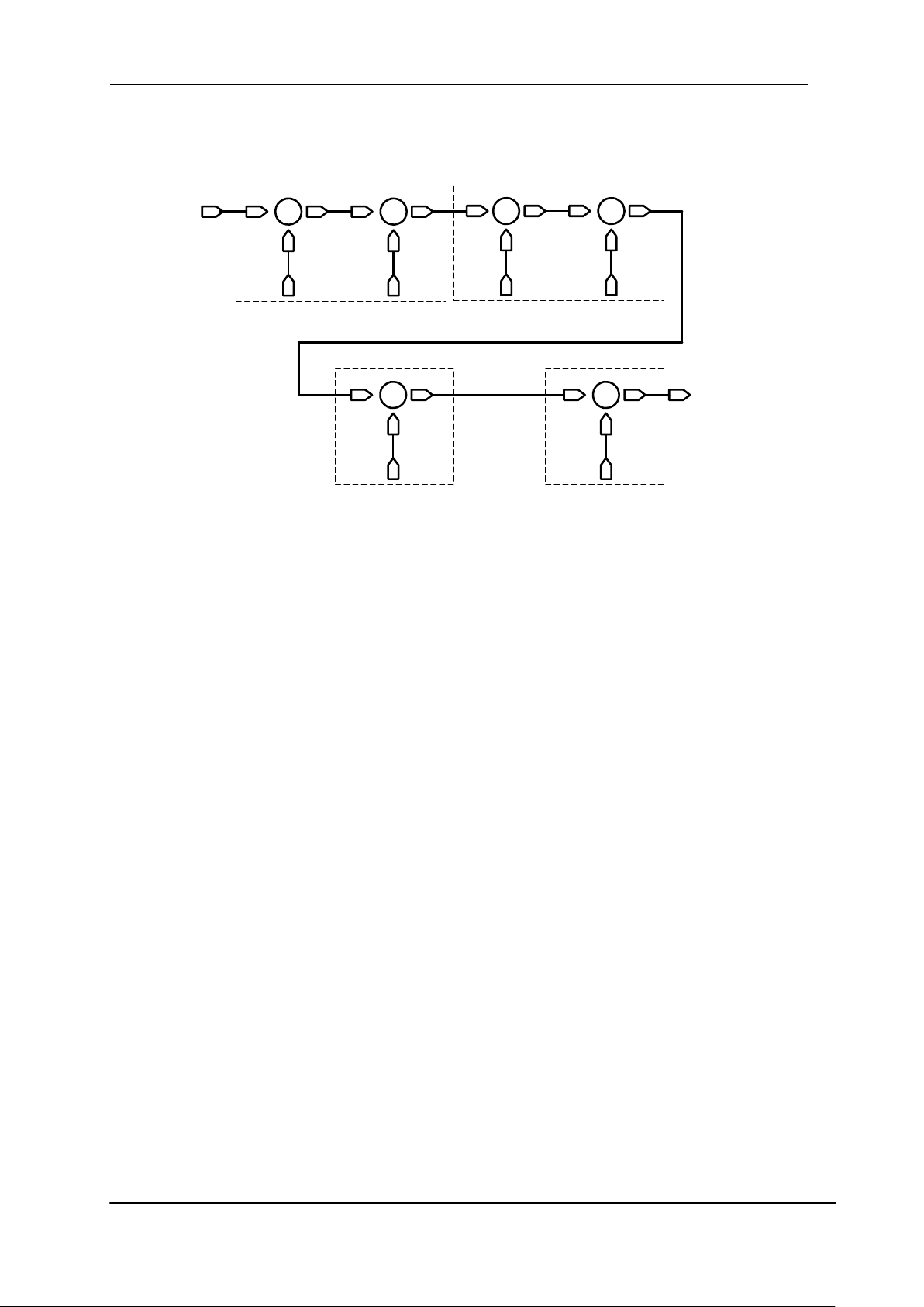
4.3 Digital Processing flow in FPGA
The digital processing flow in FPGA is shown below.
Figure 4-3-1 FPGA Processing Block Diagram
4.4 Startup
After turning on, the camera runs a startup procedure before it starts getting
images and outputting data. It takes about 15 seconds.
The startup procedure is as follows:
.
(1) The camera hardware initializes. The indicator (LED green) blinks.
(2) Reads out the latest camera settings from the flash memory. (User settings if
any or factory default settings)
(3) Set up the camera with the setting value from the flash memory.
The indicator (LED green) changes from blinking into lighting.
After those sequences, the camera is ready to get images and output data.
4.5 Saving and Loading Camera Settings
The camera settings data is saved in the internal memory (flash memory) and is
loaded from the memory when turning on the power supply or loading (sending the
“rfd” command).
Commands for rewriting the memory are as follows.
Reset to factory settings (rst)
Store present setup data in memory (sav)
Store pixel correction data in memory (wht)
XCM4085TLCT6 UME-0062-01
Page 36
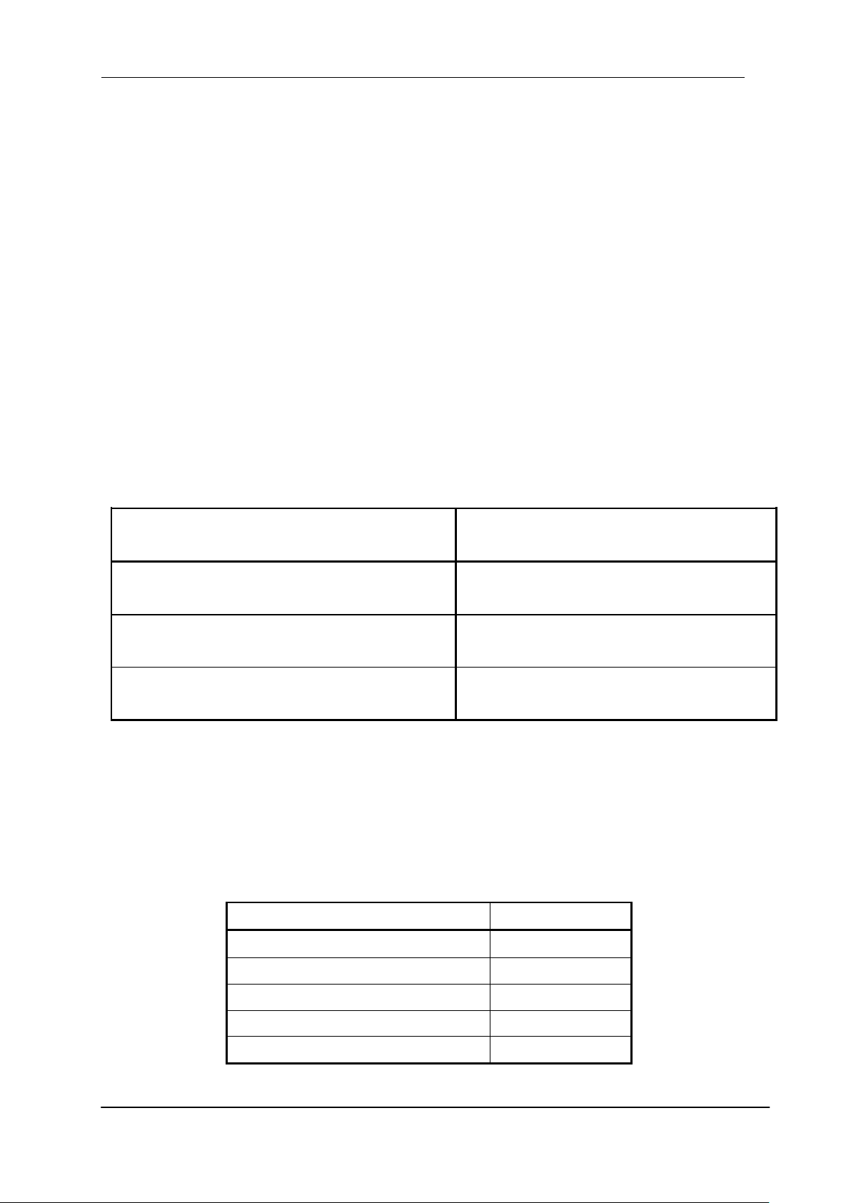
36 NED
Camera operation mode
(Exposure mode)
Control input
(From frame grabber board)
Free Run
(Programmable time setting) (Factory Setting)
Not in use
Ext Edge
(External trigger edge + Programmable time setting)
External trigger (CC1) is required
Ext Level
(External trigger level time setting)
External trigger (CC1) is required
Parameter Items
Setup Value
Communication Speed (Baud rate)
115200bps
Data Length
8bit
Parity Bit
None
Stop bit
1bit
Flow Control
None
Notes:
1) The number of times the flash memory can be rewritten will vary depending on
actual operational conditions.
2) After turning on the power supply, the camera always checks the memory status.
If the data is not within the designated range due to a malfunction or other type of
trouble, the memory will be automatically reset to the factory settings.
3) If the camera power is disconnected while rewriting the memory, the whole data
saved in the memory will be deleted.
4) As it takes several seconds to rewrite the memory, do not disconnect power
supply before receiving the answer from the camera.
5) When changing the factory setting exposure mode, be sure to send the control
input signal (CC1). If you do not send CC1 or sending control input signals are out
of the designated range, you cannot get images and cannot change the settings.
See 4.8.2 and 4.8.3.
Table 4-5-1 Camera Operation Mode and Control Input
4.6 Serial Communication Settings
Serial communication is performed through the Camera Link Interface
Table 4-6-1 shows serial communication settings.
Table 4-6-1 Serial Communication Settings
XCM4085TLCT6 UME-0062-01
Page 37
37 NED
LSB
MSB
10bit8bit
LSB
MSBbit9
bit8
bit7
bit6
bit5
bit4
bit3
bit2
bit1
bit0
8-bit(Default)
ADC
ADC
10-bit
bit9
bit8
bit7
bit6
bit5
bit4
bit3
bit2
bit1
bit0
2 4 6 8 4090 4092 4094 4096
2 4 6 8 4090 4092 4094 4096
1 3 5 7 4089 4091 4093 4095
無効 無効 無効無効無効 無効 無効無効
無効 無効 無効無効無効 無効 無効無効
無効 無効 無効無効無効 無効 無効無効
XCLK
DVAL
LVAL
1 2 3 4 2045 2046 2047 2048
1
1
1
無効 無効
無効 無効
無効 無効
1
2125CLK(25usec)min.
2125
1 3 5 7 4089 4091 4093 4095
1 3 5 7 4089 4091 4093 4095
2 4 6 8 4090 4092 4094 4096
無効 無効 無効無効無効 無効 無効無効
無効 無効 無効無効無効 無効 無効無効
無効 無効 無効無効無効 無効 無効無効 1
1
1
無効 無効
無効 無効
無効 無効
R_odd
R_even
G_odd
G_even
B_odd
B_even
2048CLK(24.1usec)
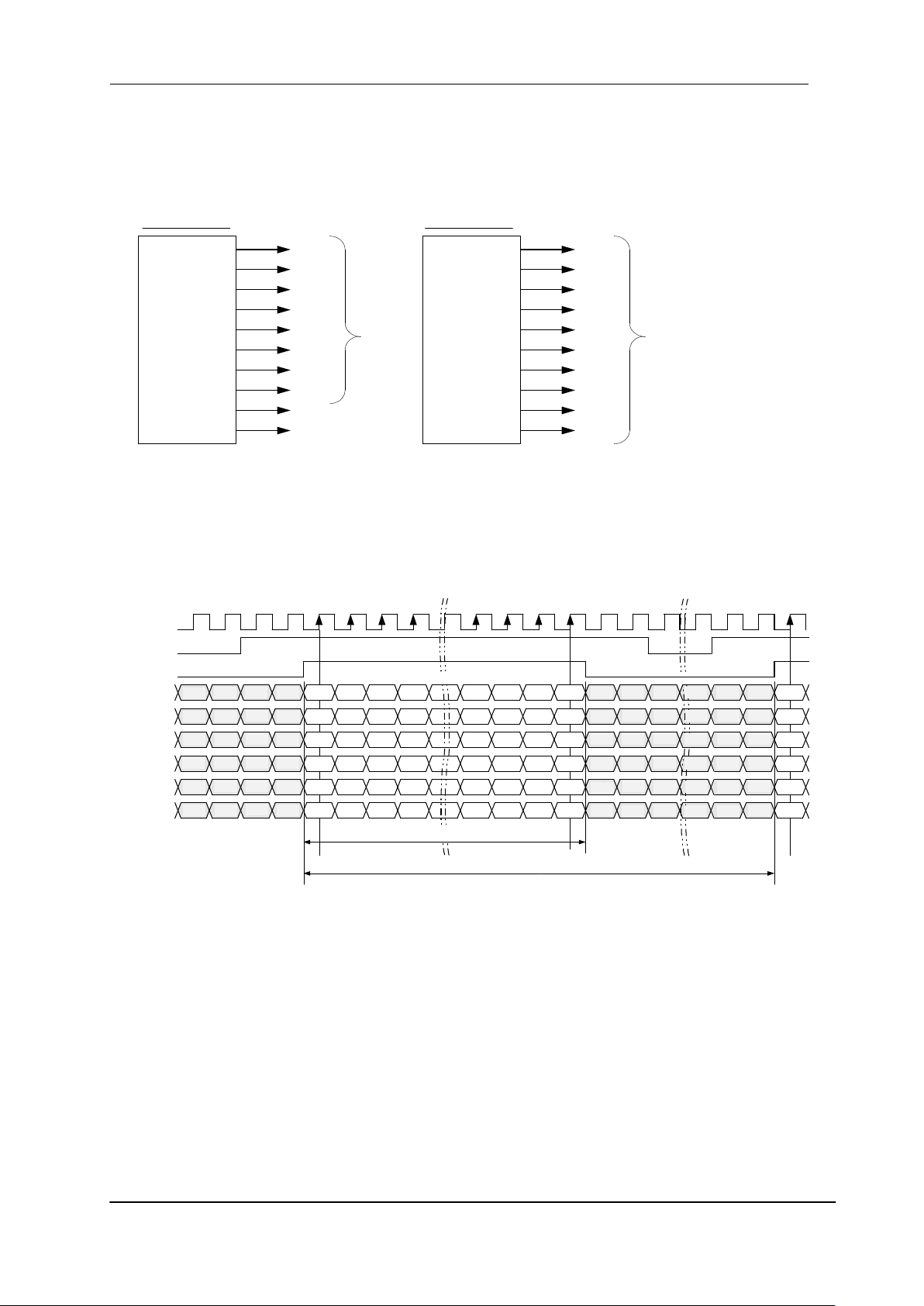
4.7 Video Output Format
The camera outputs 8-bit or 10-bit digital data.
The A/D converter of the camera has a 10-bit resolution. For 8-bit output, the
upper 8-bits of the signal can be output as video data.
Figure 4-7-1 Pin Assignments of Digital Data
Video output phase of the camera is shown below.
Figure 4-7-2 Video Output Phase of the Camera (with 85MHz 2taps at each R,G,B for data output)
XCM4085TLCT6 UME-0062-01
Page 38
38 NED
Item
symbol
XCM4085TLCT6
Programmable exposure time
P
Data output at each colour
at 85MHz 2taps:22.12~23373.17
at 85MHz 1tap:46.37~23373.17
at 40MHz 2taps:49.94~23373.17
at 40MHz 1tap:100.58~23373.17
1 2 3 4 4093 4094 4095 4096
1 2 3 4 4093 4094 4095 4096
1 2 3 4 4093 4094 4095 4096
無効 無効 無効無効無効 無効 無効無効
無効 無効 無効無効無効 無効 無効無効
無効 無効 無効無効無効 無効 無効無効
XCLK
DVAL
LVAL
R
G
B
1 2 3 4 4093 4094 4095 4096
1
1
1
無効 無効
無効 無効
無効 無効
1
4190CLK(49.3usec)min.
4190
4096CLK(48.2usec)
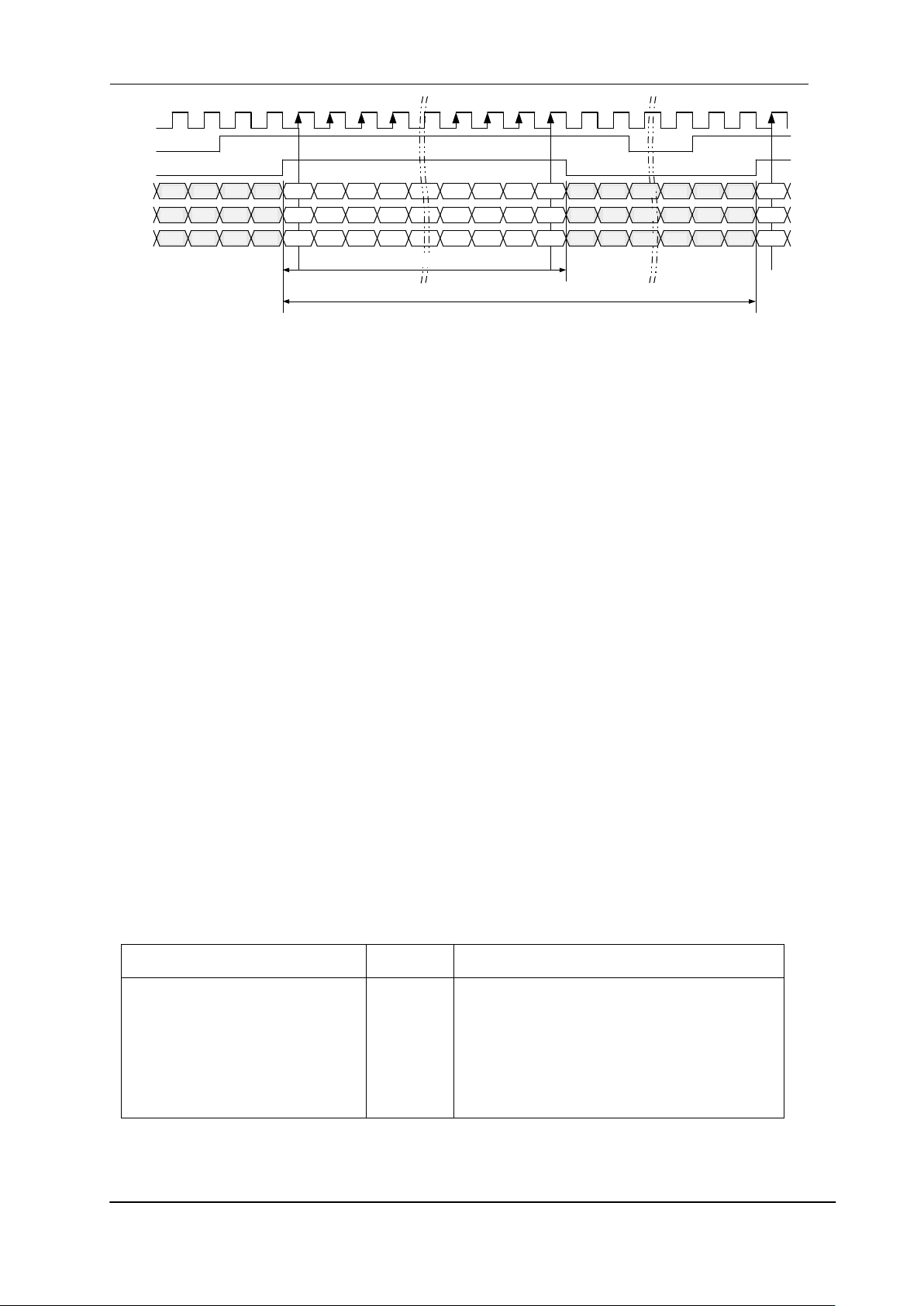
Figure 4-7-3 Video Output Phase of the Camera (with 85MHz 1tap at each R,G,B for data output)
Note:
1) FVAL = 0 (low level) fixed
2) The configurations of Camera Link interface are shown below when the following
outputs are used.
Output of 1 tap at each colour with 24 bits: Camera Link Base Configuration
Output of 1 tap at each colour with 30 bits: Camera Link Medium Configuration
Output of 2 taps at each colour with 24 bits: Camera Link Medium Configuration
Output of 2 taps at each colour with 30 bits: Camera Link Full Configuration
4.8 Exposure Mode and Timing Chart
The camera has three exposure modes. The overview of each mode and the
timing are as follows.
4.8.1 Free Run Exposure Mode (Programming time setting)
In free-run exposure mode, the camera generates its own internal control signal
based on two programmable parameters, exposure time and readout time.
Table 4-8-1-1 Programmable Exposure Time
XCM4085TLCT6 UME-0062-01
Page 39
39 NED
Readout time
R
Data output at each colour
at 85MHz 2taps:24.10
at 85MHz 1tap:48.19
at 40MHz 2taps:50.73
at 40MHz 1tap:101.45
Scan Rate
S
Data output at each colour
at 85MHz 2taps:24.97~23376.02
at 85MHz 1tap:49.22~23376.02
at 40MHz 2taps:52.79~23376.02
at 40MHz 1tap:103.44~23376.02
P
Programmable exposure time (μs)
S
Scan rate (μs)
Clock
89.722 (MHz)
Padding
4(fixed)
Dividing
64(fixed)
Counter
31~32767
露光
読み出し
LVAL
R
P
S
Exposure
Readout
LVAL
(unit:μs)
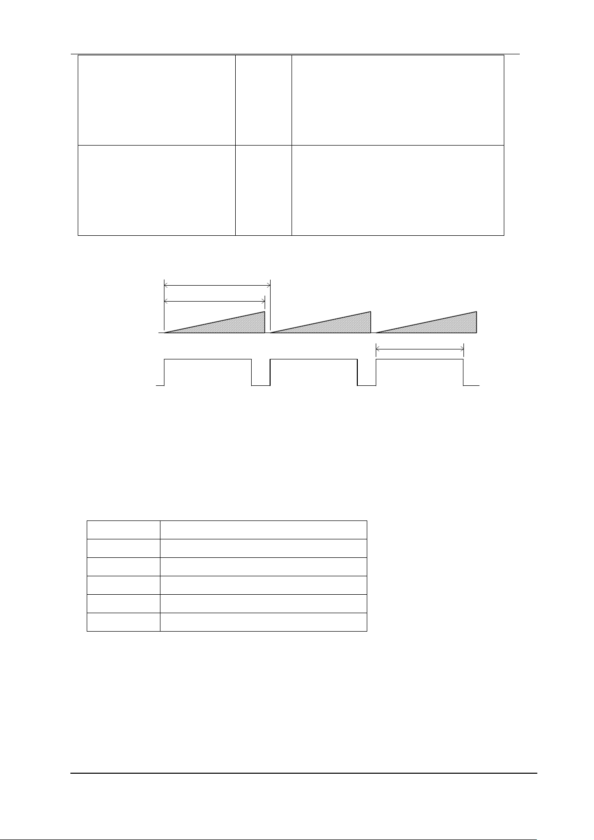
Figure 4-8-1-1 Free Run Exposure Mode
4.8.1.1 Programmable exposure setting time and calculation of scan rate
Calculation 1) P = Counter ÷ {Clock ÷ Dividing}
Calculation 2) S = P + [Padding ÷ {Clock ÷ Dividing}]
(Example)
In case of the camera is ”XCM4085TLCT6” and the command is ”int □ 64 □ 100”
Clock = 89.722,Dividing = 64,Counter = 100
Programmable exposure time (μs) = 100 ÷ {89.722 ÷ 64} =71.33
Scan rate (μs) = 71.33 + [4 ÷ {89.722 ÷ 64}]= 74.18
XCM4085TLCT6 UME-0062-01
Page 40
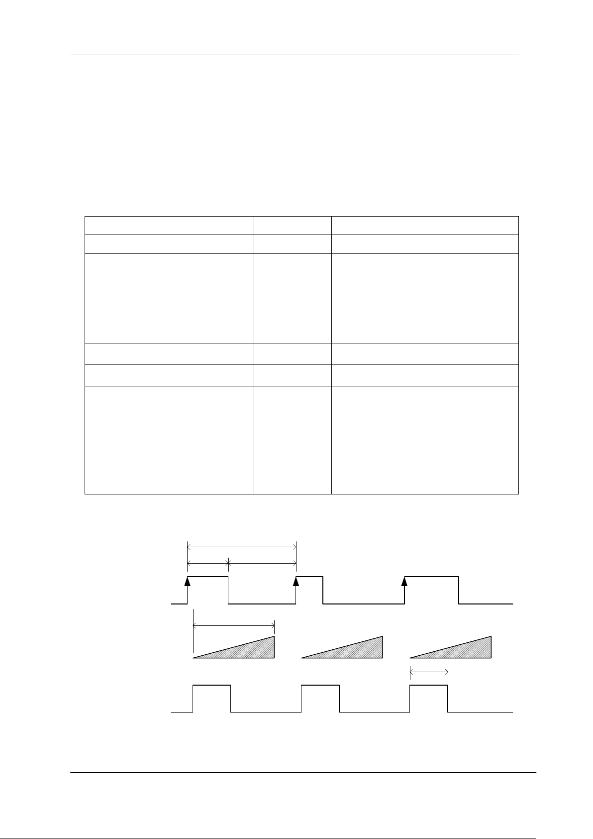
40 NED
Item
symbol
XCM4085TLCT6
Programmable exposure time
P
22.12 ~ 23373.17
Readout time
R
Data output at each colour
at 85MHz 2taps:24.10
at 85MHz 1tap:48.19
at 40MHz 2taps:50.73
at 40MHz 1tap:101.45
Trigger pulse H time
T1
≧1.50
Trigger pulse L time
T2
≧2.86
Trigger pulse cycle(Scan rate)
T3
≧P + 2.86
But the scan rate must be as follows.
Data output at each colour
at 85MHz 1tap:≧49.22
at 40MHz 2taps:≧52.79
at 40MHz 1tap:≧103.44
外部トリガ信号
入力(CC1)
T1 T2
T3
露光
読み出し
LVAL
R
P
Exposure
Readout
LVAL
External
Trigger Signal
Input(CC1)
4.8.2 External Trigger Exposure Mode (External trigger edge)
In external trigger exposure mode (Trigger Edge), the exposure time is
determined by the setting through the serial communication, each exposure starts
with the rising edge and the line period is determined by the time from rising edge
to rising edge of the trigger pulse. The range of programmable exposure time, the
timing chart of the exposure and the readout are shown below.
Table 4-8-2-1 Programmable Exposure Time
(unit:μs)
Figure 4-8-2-1 External Trigger (Trigger Edge) Exposure Mode
XCM4085TLCT6 UME-0062-01
Page 41
41 NED
Item
Symbol
XCM4085TLCT6
Readout time
R
Data output at each colour
at 85MHz 2taps:24.10
at 85MHz 1tap:48.19
at 40MHz 2taps:50.73
at 40MHz 1tap:101.45
Trigger pulse H time (Exposure Time)
T1
≧22.12
Trigger pulse L time
T2
≧2.86
Trigger pulse cycle (Scan Rate)
T3
The value of trigger pulse cycle
must be as follows.
Data output at each colour
at 85MHz 2taps:≧24.98
at 85MHz 1tap:≧49.22
at 40MHz 2taps:≧52.79
at 40MHz 1tap:≧103.44
T1 T2
T3
R
T1
外部トリガ信号
入力(CC1)
露光
読み出し
LVAL
Exposure
Readout
LVAL
External
Trigger Signal
Input(CC1)
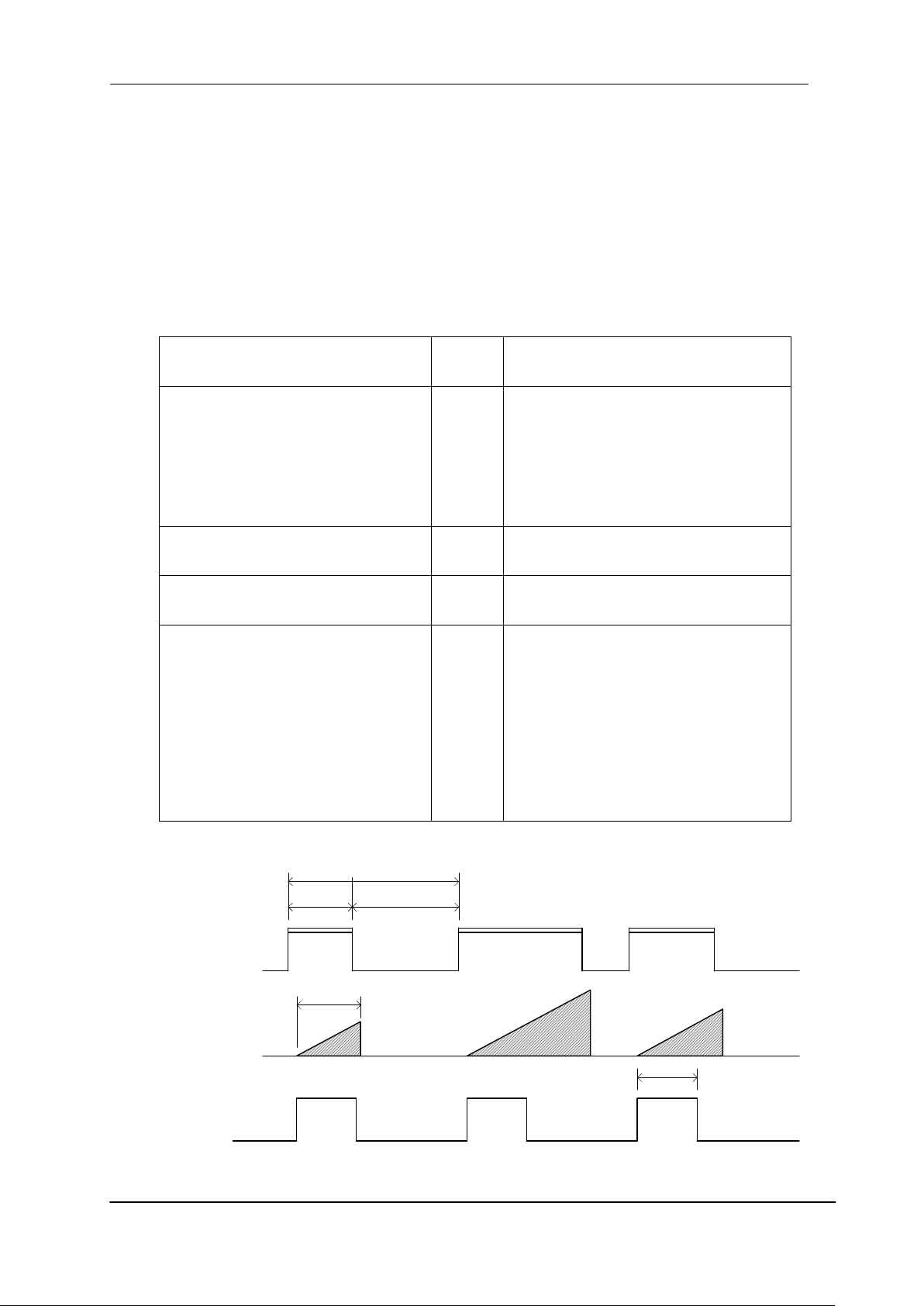
4.8.3 External Trigger Exposure Mode (Trigger Level)
In external trigger exposure mode (Trigger Level), the exposure time is
determined by the high trigger pulse time, each exposure starts with the rising edge
and the line period is determined by the time rising edge to rising edge of trigger
pulse. The range of programmable exposure time, the timing chart of the exposure
and the readout are shown below.
Table 4-8-3-1 Programmable Exposure Time (Trigger Level)
Figure 4-8-3-1 External Trigger (Trigger Level) Exposure Mode
XCM4085TLCT6 UME-0062-01
(unit:μs)
Page 42
42 NED
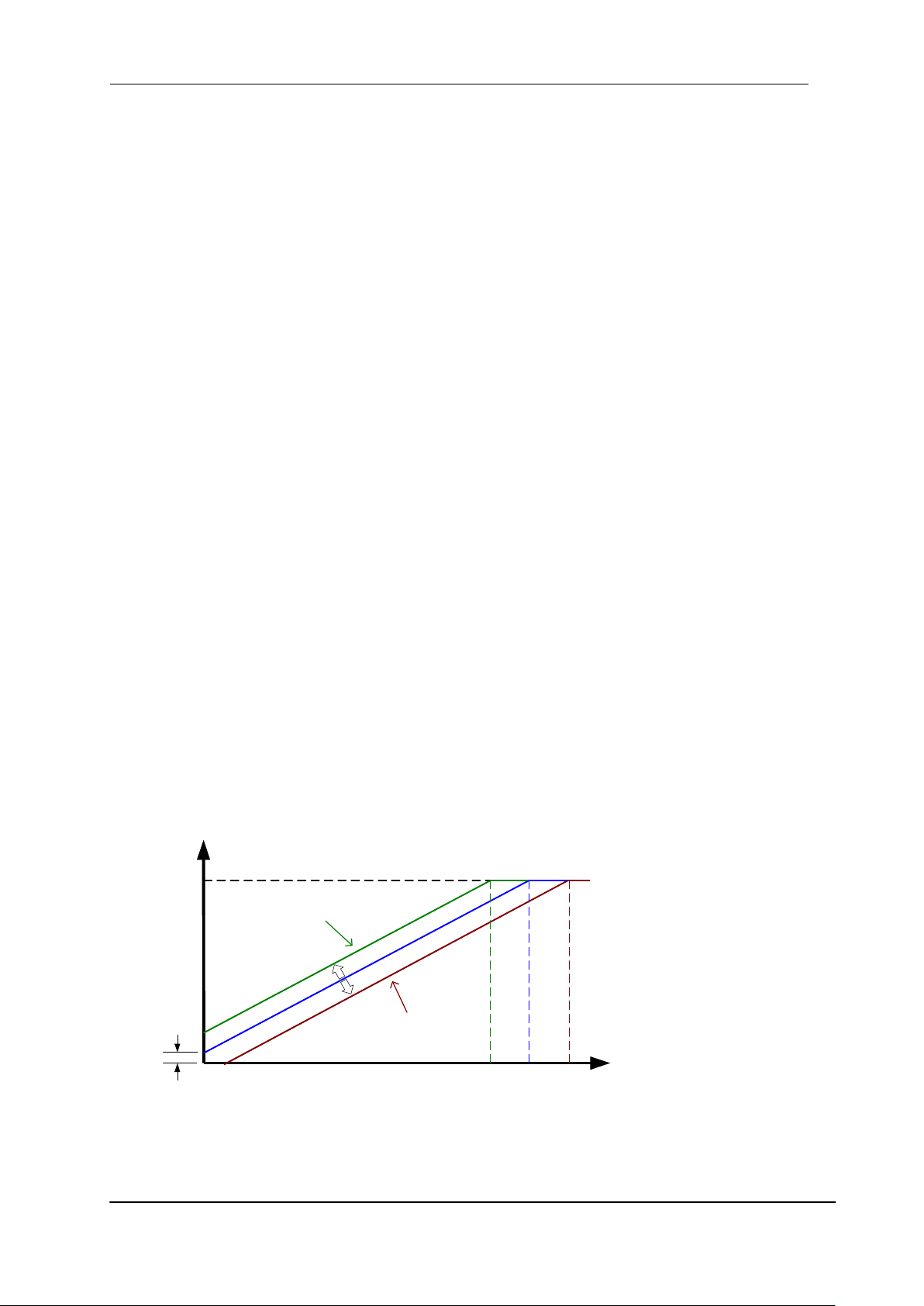
Se
Volume of Light(lx・s)
Output(DN)
Fs
:Saturation Output (DN)
Df
:Dark Current (DN)
Se
:Saturation Exposure (DN)
Fs
0
Minus offset
Plus offset
Df
4.9 Digital Gain / Offset Settings
4.9.1 Setting Digital Gain (1)
Digital gain is set with the following commands: Digital Gain (Common) “gdx”; digital
gain (R) “gdxr”; digital gain (G) “gdxg”; digital gain (B) “gdxb”. RGB (Common)
digital gain setting should be used when making small adjustments to multiple
cameras. Individual colours’ digital gain should be used for adjusting white balance
etc.
Note : Gain and noise are proportionally related. Adjust the amount of gain in
accordance with the requirements of your camera system.
4.9.2 Setting Digital Gain (2) Automatic White Balance
By automatically adjusting R, G, B gain, white balance can be adjusted. Setting is
done by sending the command “awb”. The camera calculates the average value of
the central 256 pixels, then adjusts the other 2 colours to the level of the brightest
colour. To return to the previous value, send the command “rwb” to reset each gain
level to x1.
Note : If the data change is too large, the image is saturated, or the maximum level
is exceeded, an error will occur and adjustment will be cancelled.。
4.9.3 Setting Digital Offset
Through the RGB (Common) setting, offset can be set within the range of -40 ~ +40
(DN) for 8-bit, or -160 ~ +160 (DN) for 10-bit output. Through the individual R, G, B
settings, offset can be set within the range of -20 ~ +20 (DN) for 8-bit or -80 ~ +80
(DN) for 10-bit output. Offset is set with the following commands: Offset RGB
(Common) “odx”; Offset R “odxr”; Offset G “odxg”; Offset B “odxb”.
XCM4085TLCT6 UME-0062-01
Figure 4-9-3 Saturation Exposure and Dark Current Output
Page 43
43 NED
Analog gain
Sensitivity V/ (lx・s)
1
X1
100 2 X1.5
150 3 X2
200
4
X3
300 5 X4
400 6 X5.5
550
Fs:Saturation Output(DN)
Se:Saturation Exposure(DN)
Se
Volume of Light(lx・s)
Output data(DN)
Df:Dark Current(DN)
Fs
Df
0
Minus gain
Plus gain
Note : Adjust amount of offset in accordance with the requirements of your camera
system. The gradients of lines do not change.
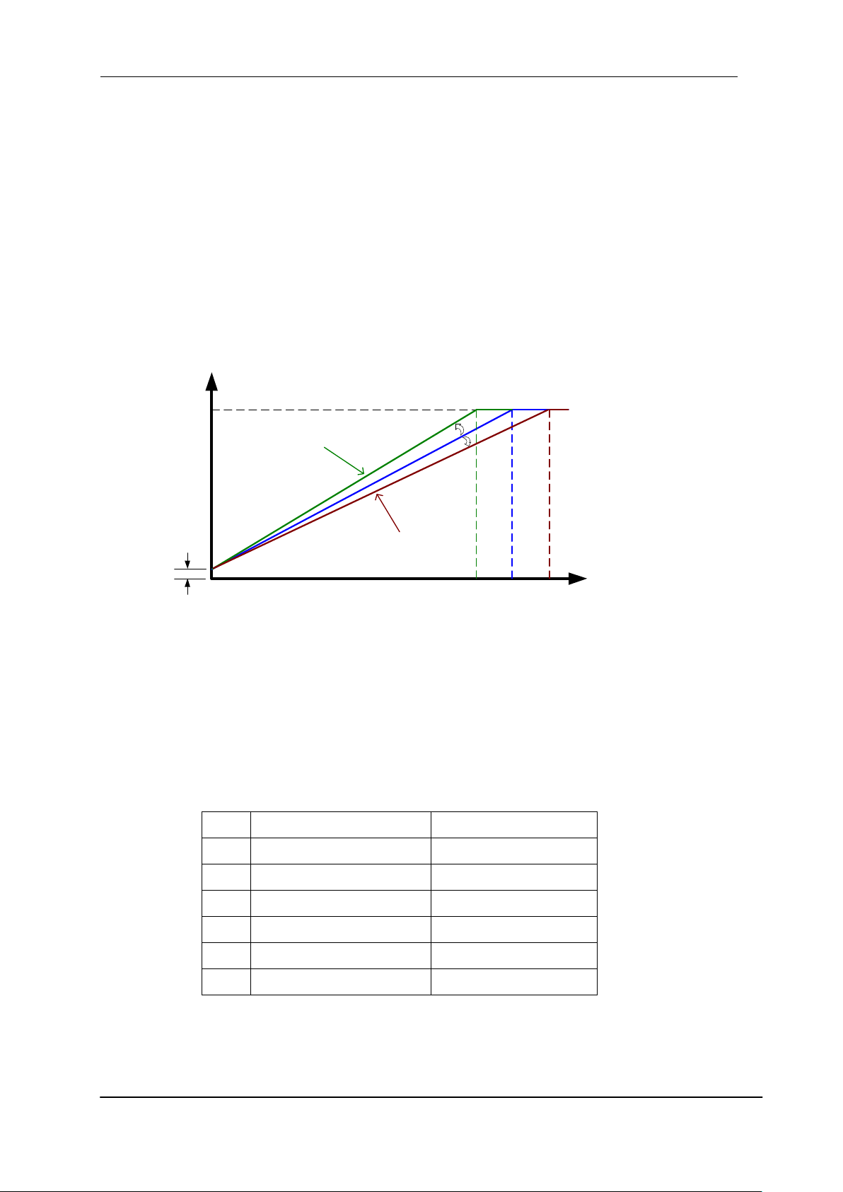
4.10 Setting Analog Gain
Gain can be adjusted by setting analog gain (6 steps, x1~x5.5) or digital gain (512
steps, x1~x2). In both cases, increasing the gain setting increases the slope of the
camera’s response curve, so that the output saturates at a lower level of light.
Conversely, with less light, a higher output can be obtained; that is to say, the
cameras sensitivity has been increased. Analog gain can be adjusted with the “gax”
command.
Gain-Sensitivity at digital gain x1, pixel correction: default, factory white correction
data is shown below.
Table 4-10-1 Gain-Sensitivity
Note:
Gain and noise values are proportionally related. Adjust amount of gain in accordance
Figure 4-10-1 Gain Adjustment
with the requirements of your camera system. We recommend using gain from x1 to
x3.
XCM4085TLCT6 UME-0062-01
Page 44
44 NED
4.11 Pixel Correction
Generally speaking, image sensors (CCD, CMOS and so on) have fixed pattern
noise and photo response non-uniformity. When you use a lens, lens shadings and
light sources also can cause non-uniformity. The camera is factory set to the
optimal correction before shipping in order to provide images of high grade. The
camera also has a user white correction function in order to cope with lens shading
and non-uniform illumination.
Cal_bl : Output data of each pixel in perfect dark (factory correction)
Cal_wh : Output data of each pixel in uniform illumination (factory correction)
or when viewing a subject for correction (user white correction)
Target_Val : Target value for user correction (10bit output conversion value)
Fix_bl : Fixed value 32DN (10bit output conversion value)
Vin: Input data (Before correction) Vout :Output data (After correction)
The corrected data is expressed by the following equation.
Vout=[(Vin-Cal_bl) x (Target_val-Fix_bl) / (Cal_wh-Cal_bl)] + Fix_bl
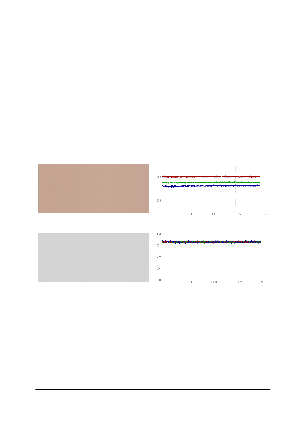
Image “before” user arbitrary pixel is corrected. Luminance Profile of left image
Image “after” user arbitrary pixel is corrected Luminance Profile of left image
Figure 4-11-1 Waveform and image before and after bit correction
XCM4085TLCT6 UME-0062-01
Page 45

45 NED
4.11.1 Operating Procedure
Pixel Correction settings are done for either User Arbitrary Correction Data 1 or 2.
Send the command “shc2 CR” or “shc3 CR” via the COM port; User Arbitrary
Correction Data will be made active.
Place a uniformly white object fully in the camera view. Now we can acquire User
Arbitrary Correction Data (gray). When this is done with the lens attached, lens and
illumination shading will also be corrected at the same time. However, dark and light
details of the white object will be picked out, so the lens should be defocused. Next,
send the command “wht CR” over the COM port. The camera should return “>OK”
“>wht”. Now the User Arbitrary Correction Data (gray) has been written to the
camera’s flash memory.
To set the pixel correction target value, proceed as below:
Send the command “MurVal CR” via the COM port. The camera should return
“>OK” “>Mur” “>Val”. With this, the pixel correction target value R is set.
Send the command “MugVal CR” via the COM port. The camera should return
“>OK” “>Mug” “>Val”. With this, the pixel correction target value G is set.
Send the command “MubVal CR” via the COM port. The camera should return
“>OK” “>Mub” “>Val”. With this, the pixel correction target value B is set.
Notes:
1) For “Val” above, substitute the target value, 0~1023 (10-bit).
2) The pixel correction target value should be set slightly higher than the obtained
image brightness in order to attain the full range of output.
4.12 Adjusting White Balance
The white balance on this camera has been adjusted without lens and mount, and
using a daylight fluorescent light. Depending on the lens and light source you use, it
may be necessary to adjust the white balance in one of the two ways described
below.
Note: In the following cases, please use the pixel (bit) correction function:
If a variable responsivity pattern appears across the image when using a light source
that does not have a broad wavelength, such as a 3-wavelength fluorescent lamp.
The difference between the colour levels is large, and exceeds the maximum value of
digital gain.
4.12.1 Pixel (Bit) Correction Function
Correct the white balance using the User White Correction function(see 4.11)
4.12.2 Digital Gain Function
Adjust the white balance by adjusting the digital gain of each RGB colour.(see
4.9.1)Adjust automatically using the automatic white balance function(see 4.9.2)
XCM4085TLCT6 UME-0062-01
Page 46
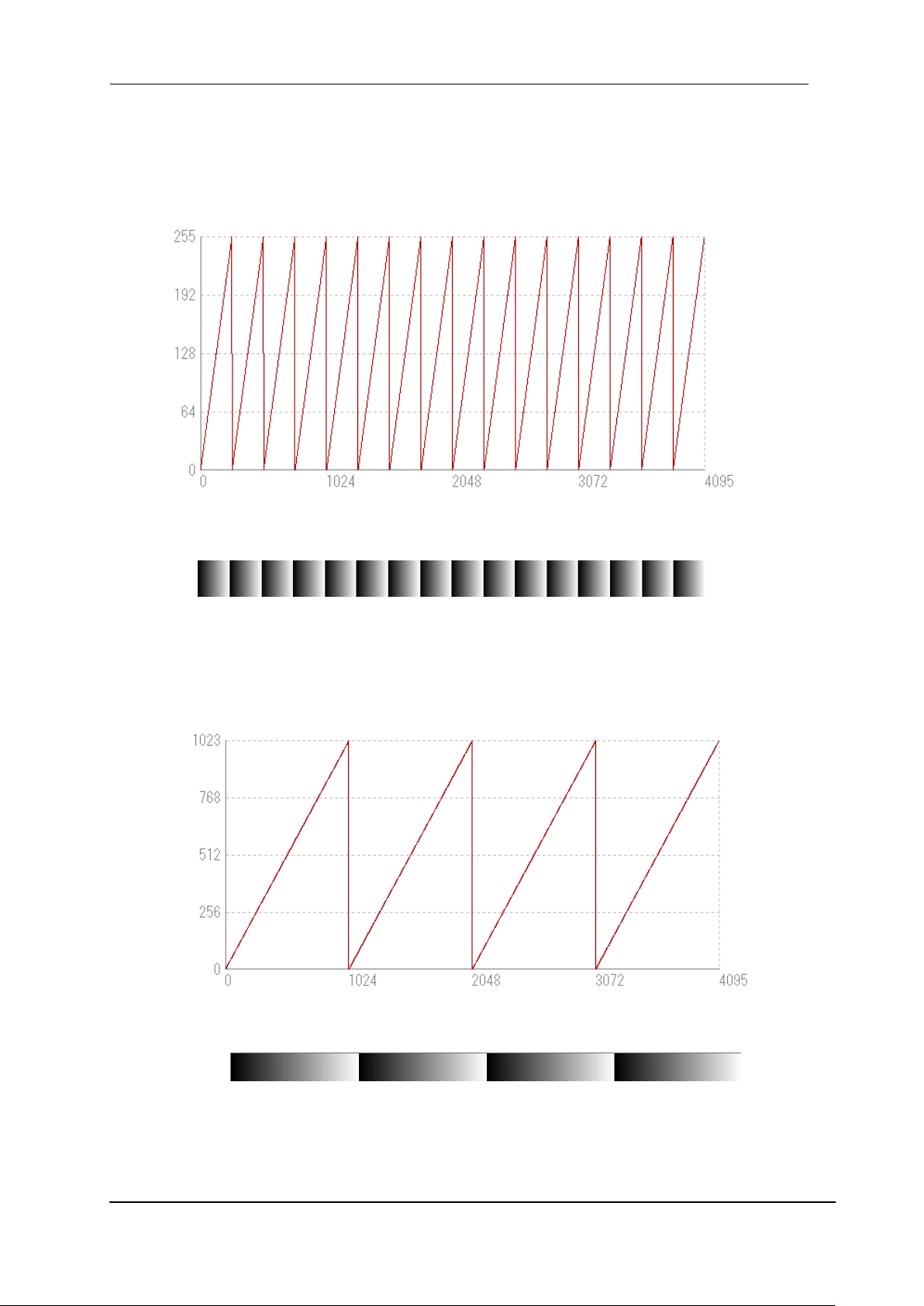
46 NED
4.13 Test Pattern
The test pattern can be used to check whether your system is correctly receiving
the camera data.
The gray test patterns for 24 and 30-bit colour are shown below.
Figure 4-13-1 24-bit Colour Gray Test Pattern
Figure 4-13-2 24-bit Colour Gray Test Image
Where pixel 0 has the value 0DN, the value increases by 1DN each pixel, up to
255DN, then the pattern repeats.
Figure 4-13-3 30-bit Colour Gray Test Pattern
Figure 4-13-4 30-bit Colour Gray Test Image
Where pixel 0 has the value 0DN, the value increases by 1DN each pixel, up to
1023DN, then the pattern repeats.
XCM4085TLCT6 UME-0062-01
Page 47
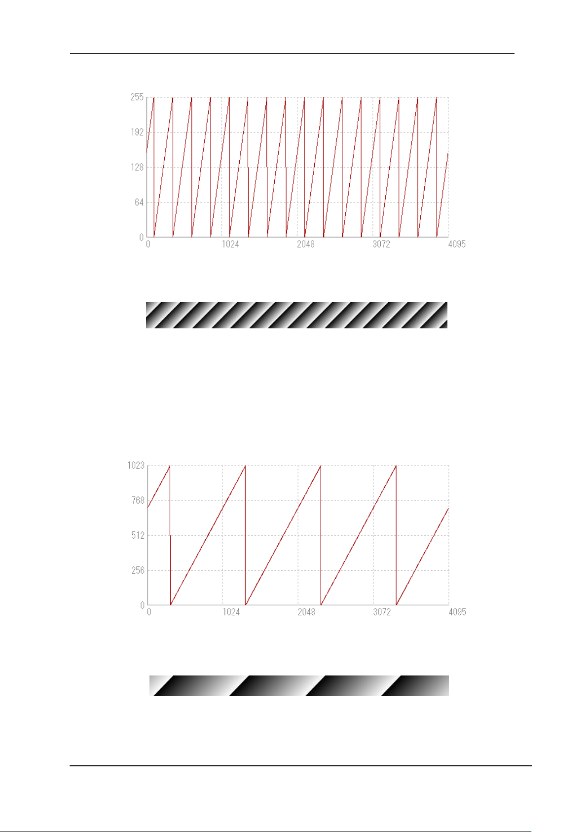
47 NED
The gray XY test pattern for 24 and 30-bit colour are shown below.
Figure 4-13-5 24-bit Colour Gray XY Test Pattern
Figure 4-13-6 24-bit Colour Gray XY Test Image
The value increases by 1DN each pixel, up to 255DN in both X-direction and
Y-direction(downward), then the pattern repeats.
Figure 4-13-7 30-bit Colour Gray XY Test Pattern
Figure 4-13-8 30-bit Colour Gray XY Test Image
The value increases by 1DN each pixel, up to 1023DN in both X-direction and
Y-direction(downward), then the pattern repeats.
XCM4085TLCT6 UME-0062-01
Page 48
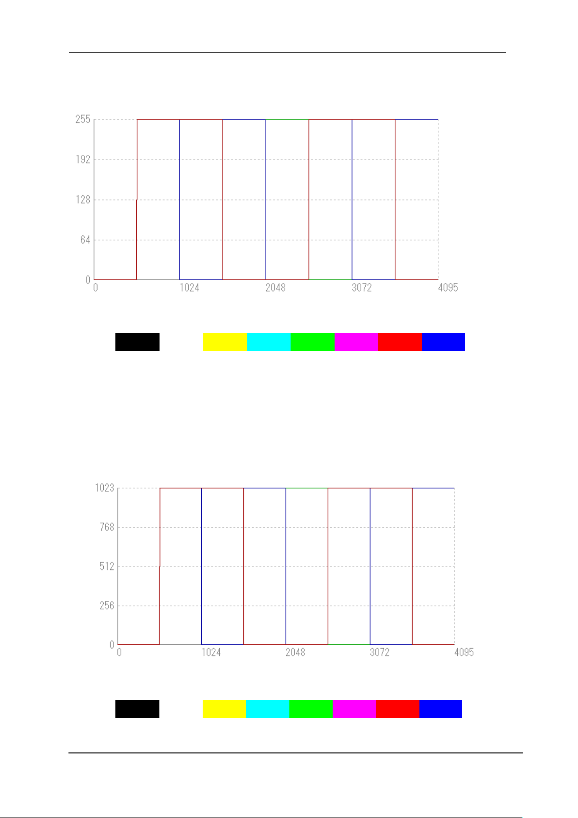
48 NED
The Colour 24-/30-bit colour bar test pattern is shown below.
Figure 4-13-9 24-bit Colour Bar Test Pattern
Figure 4-13-10 24-bit Colour Bar Test Image
From the first pixel, the image is a sequence of blocks of 512 pixels: Black (R:0 G:0
B:0), White (R;255, G:255, B:255), Yellow (R:255 G:255 B:0), Aqua (R:0 G:255 B:255),
Green (R:0 G:255 B:0) Pink: (R:255 G:0 B: 255), Red (R:255 G:0 B:0), Blue (R:0 G: 0
B:255)
Figure 4-13-11 30-bit Colour Bar Test Pattern
Figure 4-13-12 30-Bit Colour Bar Test Image
XCM4085TLCT6 UME-0062-01
Page 49
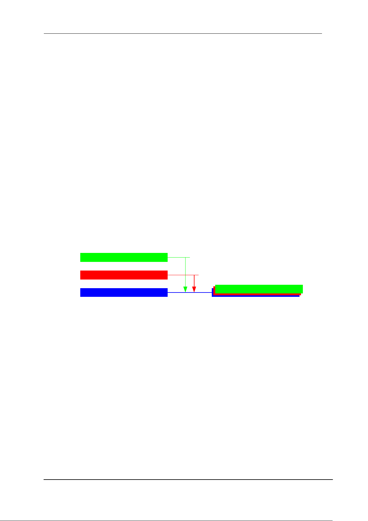
49 NED
From the first pixel, the image is a sequence of blocks of 512 pixels: Black (R:0 G:0
B:0), White (R;1023, G:1023, B:1023), Yellow (R:1023 G:1023 B:0), Aqua (R:0
G:1023 B:1023), Green (R:0 G:1023 B:0) Pink: (R:1023 G:0 B: 1023), Red (R:1023
G:0 B:0), Blue (R:0 G: 0 B:1023)
4.14 Line Delay Correction Setting
Three (3) line sensors of this camera are located laterally at one line interval.
Therefore, each RGB output data produces the image which is delayed for two pixels
in movement direction in case of an image of 1:1 reduced scale ratio of length and
width.
This can be used for correcting the deviation of delay between output datas of each
colour at the unit of one line.
For example, when an imaging object moves from the bottom to the upper direction
for a camera in case of an image of 1:1 reduced scale ratio of length and width and
“ldly □ 2” of command is sent, the image can be corrected on the deviation of delay.
When an imaging object moves from the top to the lower direction, “ldly □ -2” as of
command should be sent.
ldly□0 ldly□2
4 line output delay
2 line output delay
Figure 4-14-1 Line Delay Correction
XCM4085TLCT6 UME-0062-01
Page 50
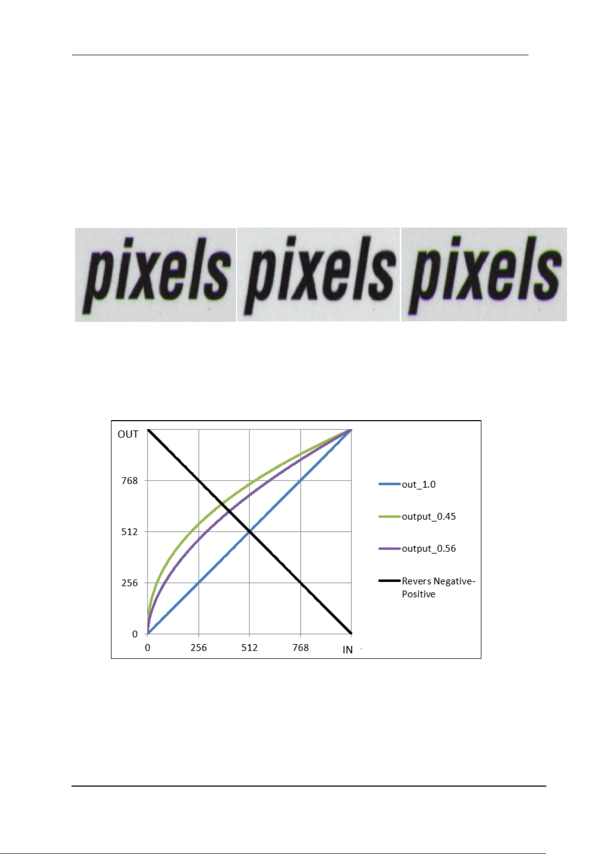
50 NED
4.15 Line Fine Adjusting Correction Setting
The Line delay correction setting on 4.14 can be used for correcting the deviation of
delay between output datas of each colour at the unit of one line.
This line fine adjusting correction can be used at the unit of a half of line by the
corrective calculation.
For example, when the colour shift still generates even if “ldly□2” and “ldly□3” of
commands are sent, “ldlys □ 5” of command may improve the colour shift.
When the value of the command is minus (-), the correction value of “Idly” becomes smaller.
ldly□2 ldly□2 and ldlys□5 ldly□3
Figure 4-15-1 Line Fine Adjusting Correction
4.16 Gamma Correction Setting
Switches Gamma correction value.
Figure 4-16-1 Gamma Correction Characteristics
XCM4085TLCT6 UME-0062-01
Page 51
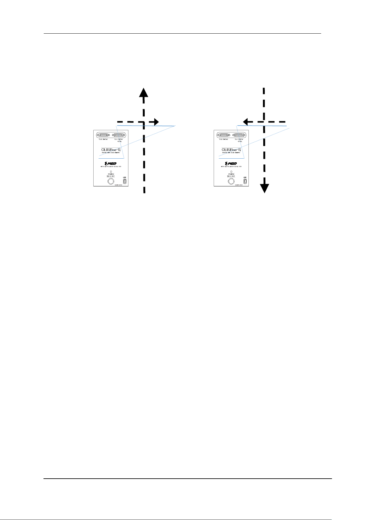
51 NED
4096
1
4096
1
Forward
Web Direction
Movement
Reverse
Web
Direction
4.17 Camera Scan Readout Direction Setting
The camera scan readout direction can be changed from forward to reverse, or vice
versa.The correlation between the camera scan readout direction and web (object
movement) direction is shown below.
① Forward Camera Scan ②Reverse Camera Scan
Readout Direction Readout Direction
Figure 4-17-1 Correlation of Camera Scan Readout Direction and Object Movement Direction
XCM4085TLCT6 UME-0062-01
Page 52
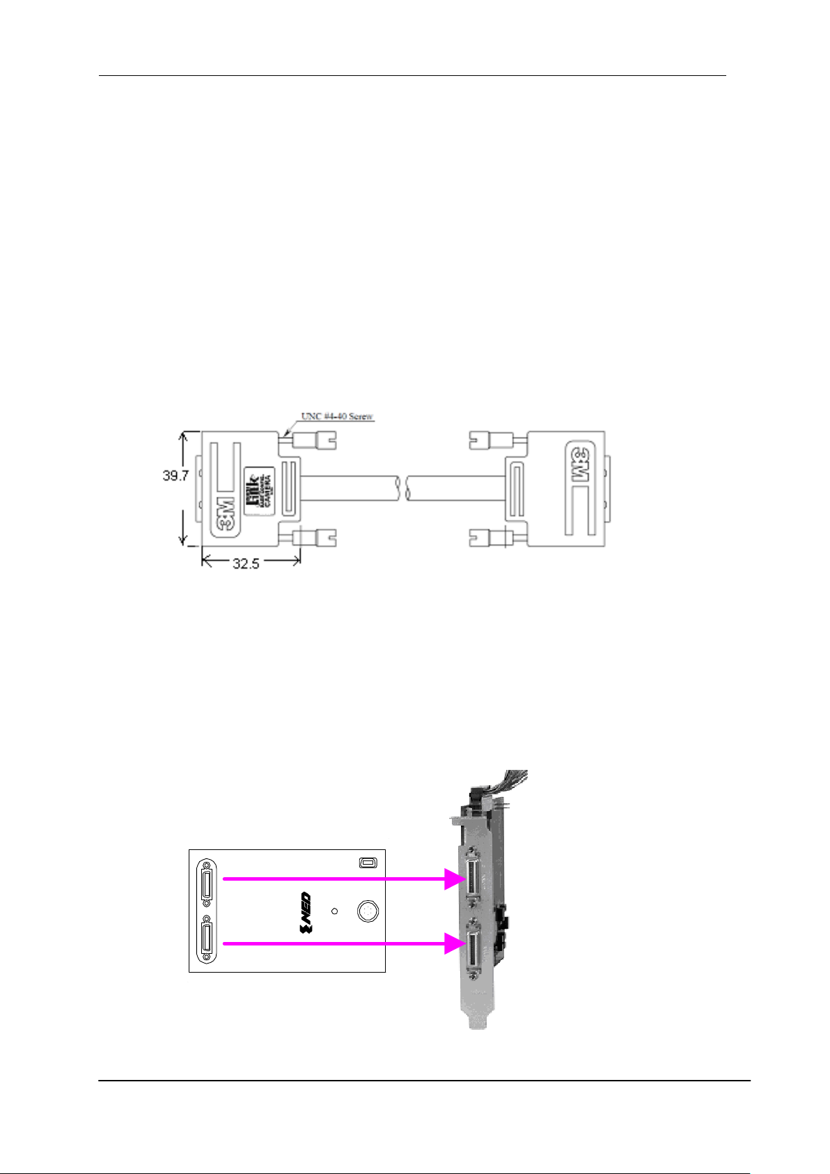
52 NED
CHANNEL #0
CHANNEL #1
CL1
CL2
POWER
DC12-15V
MADE IN JAP AN
CLISBee-S
DIGITAL LINE SCAN CAMERA
NIPPON ELECTR O-SENSOR Y DEV ICES C ORP.
CL1: DATA1
CTRL
CL2: DATA2
USB
Camera side
Frame grabber side
5 Confirming Camera Settings
5.1 Before Power-on
Please check the exterior for any damages that may have been caused during
transportation or handling etc.
① Confirm the pin assignment of the power cable. (See table 3-3-2 and Figure 3-3-4)
② Confirm the direction and the channel of the cables. Some Camera Link cables are
directional.
Note:
There is something that the connection direction is specified in the Camera Link cable.
If one of the connectors says “Camera side”, connect it to the camera.
Figure 5-1-1 Connection Direction of Camera Cable
③ Confirm the connection with the Camera Link cable and frame grabber.
The connection channel of in case of “Solios”
Camera side connector CL1 and frame grabber side connector CHANNEL#0 are
connected. Camera side connector CL 2 and frame grabber side connector
CHANNEL#1 are connected.
Figure 5-1-2 Channel of Camera Link Cables
XCM4085TLCT6 UME-0062-01
Page 53
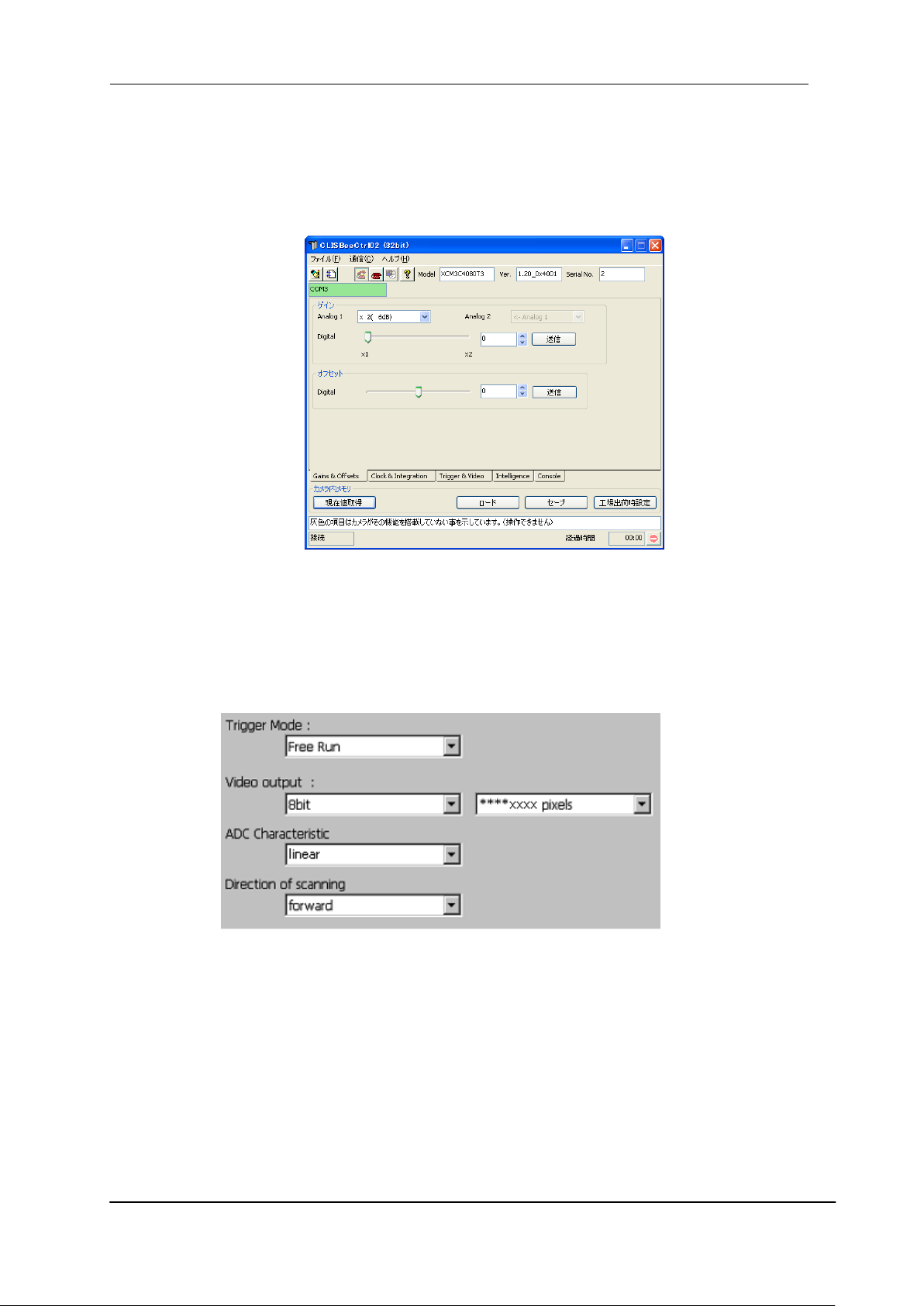
53 NED
5.2 After Power-on
(1) Confirm sent and received commands using the camera control utility. Launch
CLISBeeCtrl, set COM port and connect. Click “Memory Dump” and wait for the
response.
Figure 5-2-1 Confirmation of Connection
(2) Set a trigger mode and a video output mode with the camera control utility.
Figure 5-2-2 Setting of Exposure Mode and Video Output Mode
XCM4085TLCT6 UME-0062-01
Page 54
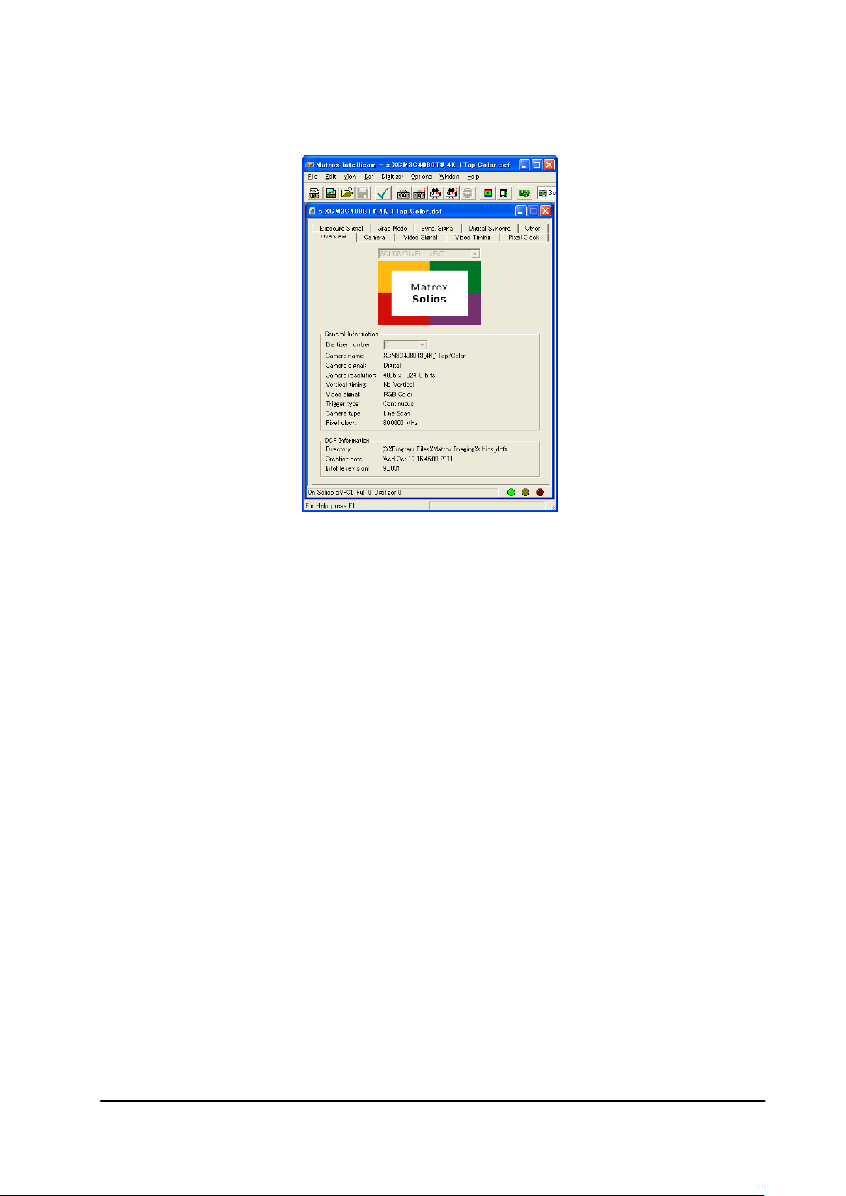
54 NED
(3) Capture images using a camera interface board utility. In case of Matrox’s Solios, it
is convenient to use Intellicam.
Figure 5-2-3 Solios Intellicam dcf Window
5.3 In Operation
(1) Does acquisition time out error occur?
<Cause>
①Captured images are too heavy.
Note: If there are many filtering processes, the assignments to the driver may be
insufficient.
②The cables are detached from the connector.
Note: that the power cable and Camera Link cables are connected to the
camera correctly.
③ Camera Link cables come under the influence of noise when the cables are
laid near a light source inverter line or a power line.
Note: The personal computer in use may be reset.
(2) Are there dark lines in the direction of vertical scanning on the image?
<Cause>
Dust on the sensor window.
Note: Dust may come on the sensor window from the inside or the outside of the
camera. Remove the dust with air or a lens cleaner.
XCM4085TLCT6 UME-0062-01
Page 55

55 NED
6 Sensor Handling Instructions
6.1 Electrostatic Discharge and the Sensor
CMOS sensors are susceptible to damage from electrostatic discharge and can
become defective.
6.2 Protecting Against Dust, Oil and Scratches
The CMOS sensor window is part of the optical path and should be handled like
other optical components with care. If you use the camera in a dusty area, prepare
a dust-proof enclosure. Dust can obscure pixels, producing dark lines on the
image.
6.3 Cleaning the Sensor Window
Dust: Can usually be removed by blowing the window surface using a
compressed air blower.
Oil: Wipe the window with a lint-free cloth wiper moistened with ethyl alcohol
carefully and slowly.
XCM4085TLCT6 UME-0062-01
Page 56
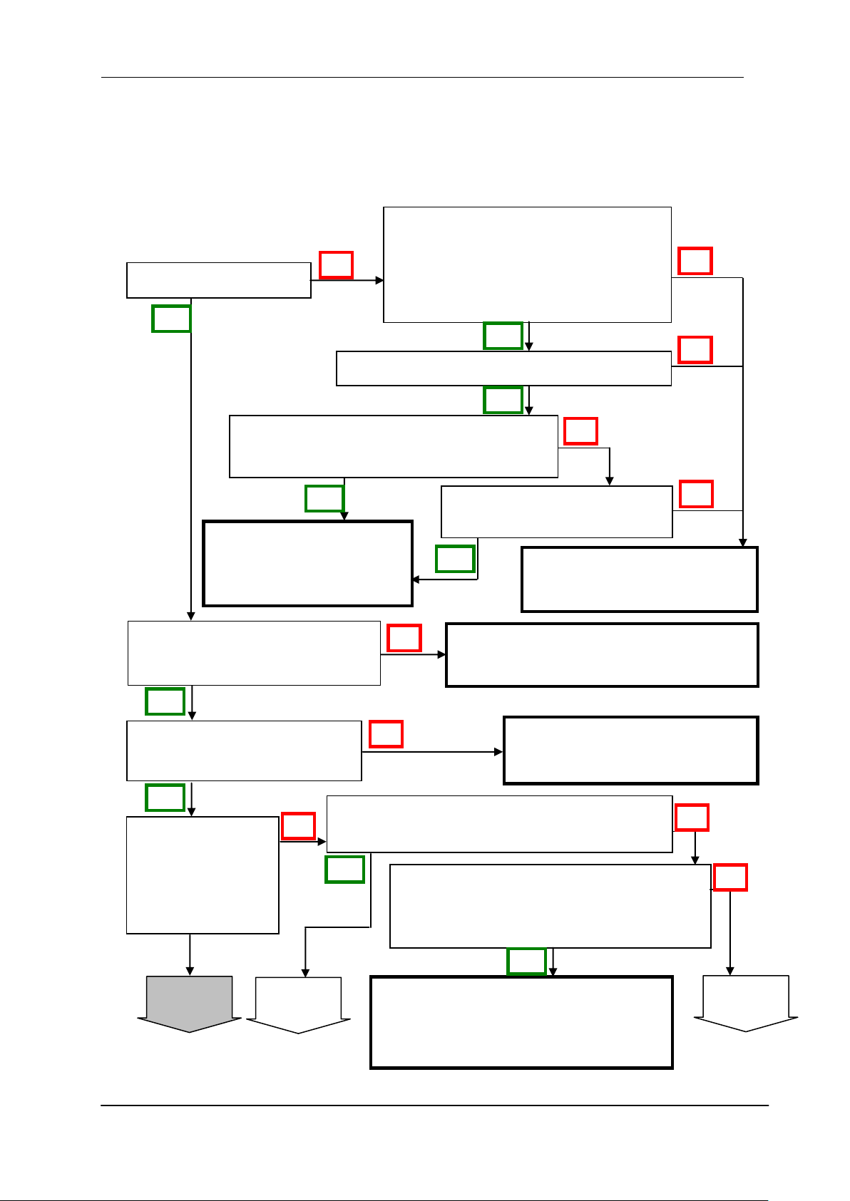
56 NED
The indicator is glowing.
Are the correct connectors being used
between the camera and the power
supply, and are they properly
connected?
Arrange a power source that
meets the specifications.
The camera has the correct
connection with the frame grabber.
The camera could be
faulty. Please contact us
for assistance.
When switched on, the power source meets
the specified voltage.
The capacity of the power
source is enough.
Connect the camera and the frame
grabber board with camera cables.
After being energized, set up the
frame grabber board suitably.
Is the sample software program being used to
control the camera.
The sample software program is used to
control the camera and is communicating
with the camera successfully.
Confirm the communication software,
the control protocol for the camera and
commands.
The power source meets the specified voltage.
The frame grabber board is
switched on and set up.
Yes
The frame grabber
is communicating
with the camera
successfully.
Yes
Yes
No
No
Yes
No
No
No
Yes
No
No
No
No
No
Yes
Yes
Yes
Yes
To next page
B
To next page
A
To next page
B
7 Troubleshooting
The following pages contain several troubleshooting charts that can help you find the
cause of problems users sometimes encounter.
7.1 When there is no Image
XCM4085TLCT6 UME-0062-01
Page 57
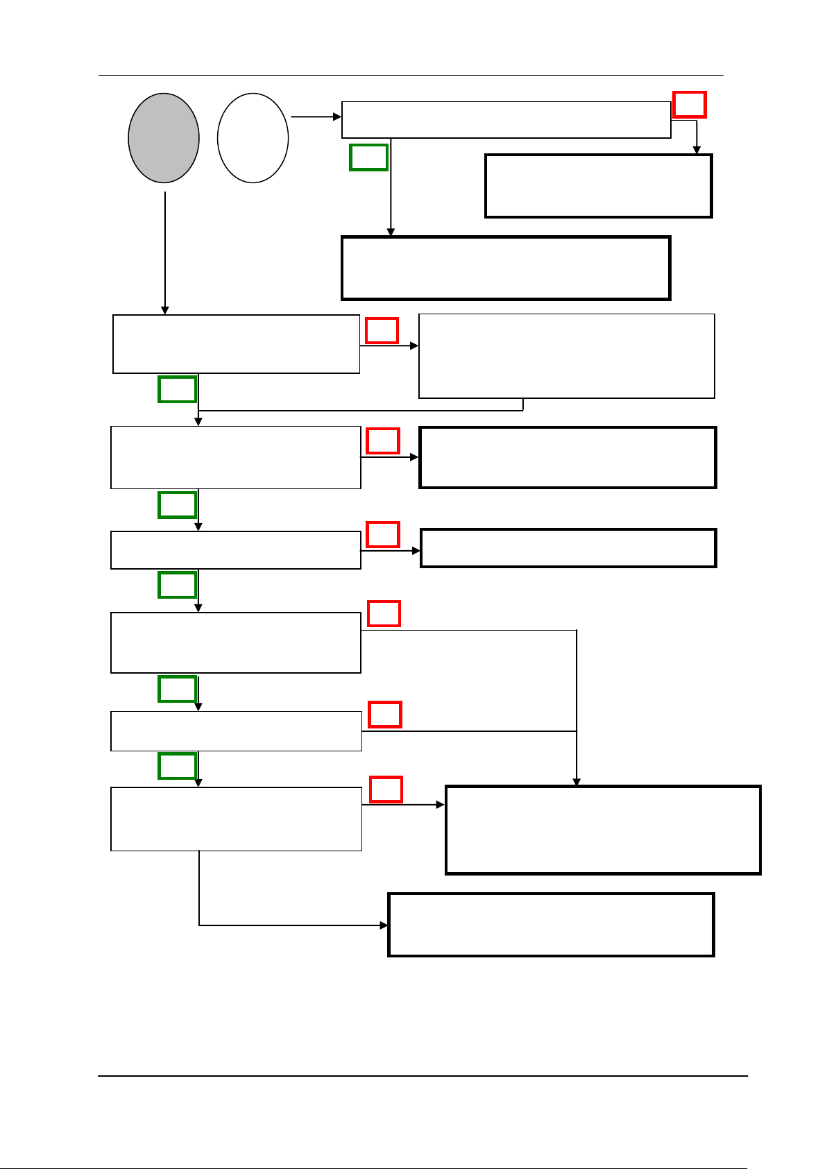
57 NED
The capturing software program is
custom made.
No image is captured with the
sample software program provided.
The communication port is set correctly.
Nothing blocks off the light.
If a lens cap is on, take it off.
The amount of the illumination is
enough.
Check the light source. If the images are
too dark, try to increase the light intensity,
and vice versa.
No image at the full aperture.
The optical axes of the camera and
the image sensor are aligned.
Check the compatibility between the
camera and the frame grabber board.
The capturing software program is
provided with the board as a sample
program.
Set the communication port
correctly.
The camera could be faulty. Please contact
us for assistance.
The camera could be faulty. Please contact
us for assistance.
No
Yes
No
Yes
No
No
Yes
Yes
Yes
Yes
No
No
No
B
A
XCM4085TLCT6 UME-0062-01
Page 58
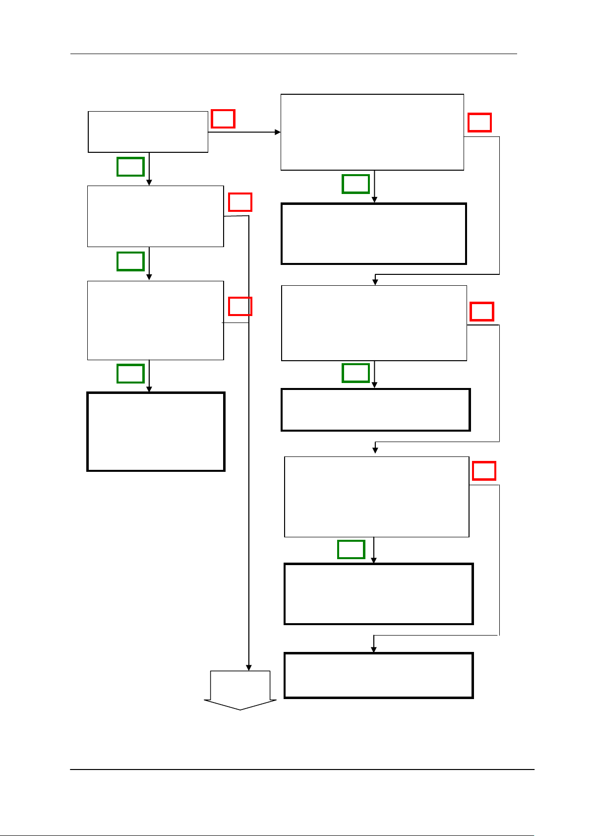
58 NED
Noise is present at the
point of first use.
A servomotor or a
magnetic valve is placed
near the camera.
The camera has been used for 3 or
more years, or the ambient
temperature is higher than room
temperature.
There are some degradable parts
in the camera. Please contact us
for assistance.
The power supply has been used for
3 or more years, or the ambient
temperature is higher than room
temperature.
Check the condition of the power
supply.
The camera and or cables are used
in a moving environment (attached
to a machine which applies stress to
the cables).
Check the condition of the camera
cables and the power supply
cable.
The camera could be faulty. Please
contact us for assistance.
Turning on a servomotor
or a magnetic valve
generates an electric
noise.
Prevent the noise
source from disturbing
the camera cables and
the power cable.
Yes
No
Yes
No
No
No
Yes
Yes
Yes
No
No
Yes
To next page
C
7.2 When Noise is present in the Image
XCM4085TLCT6 UME-0062-01
Page 59
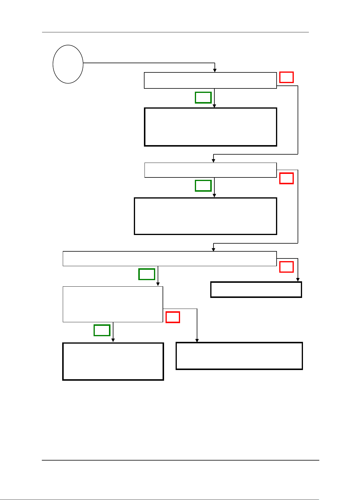
59 NED
Cables are asymmetric such as thin cables.
One of the connectors of an asymmetric
camera cable is to be connected with a
camera. (Labeled as “Camera side”)
The camera cables are too long.
Use camera cables in accordance with the
transmission rate. The cables should not be
too long to avoid the noise disturbance.
The power source has no fluctuation in voltage and is not deteriorated.
Use a stable power supply.
The camera could be faulty. Please
contact us for assistance.
When the camera gain is on a
high level, bright spots occur
without incident light.
Secondary radiation (rays)
could cause bright spots, but
this is not malfunction.
C
No
Yes
Yes
No
No
Yes
Yes
No
XCM4085TLCT6 UME-0062-01
Page 60
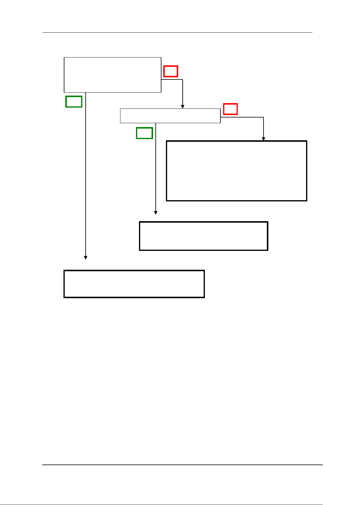
60 NED
The camera is too hot to touch.
The consumption current of the
power supply is larger than the
rating.
The camera will become hotter than the
ambient temperature while in operation
because of self-heating. Allow sufficient
air circulation around the camera to give it
the longer life.
Keep the ambient temperature within
the range of the specifications.
The camera could be faulty. Please contact
us for assistance.
Yes
No
No
Yes
7.3 When the Camera becomes hot
XCM4085TLCT6 UME-0062-01
Page 61

61 NED
8 CLISBeeCtrl
8.1 Overview
The CLISBeeCtrl is the remote control software for “CLISBee*” camera using “NED
Camera Control Protocol” (NCCP) from a PC.
Connectable interfaces are following.
1)Camera Link API
2)Communication Port (Including a virtual COM port provided by the Frame
grabber)
8.2 System Requirements
PC: PC/AT compatible
Operating System: Microsoft Windows XP or 7.
Free disk space: 1-2MB (It may fluctuate with the number of camera parameter
files.)
Connection: Camera Link frame grabber board, Camera Link cables
8.3 Install
Copy the CLISBeeCtrl folder in the media (CD-ROM, etc.) which our company
provides, to your hard disk.
8.4 Uninstall
Remove the CLISBeeCtrl folder and all files in CLISBeeCtrl folder.
XCM4085TLCT6 UME-0062-01
Page 62
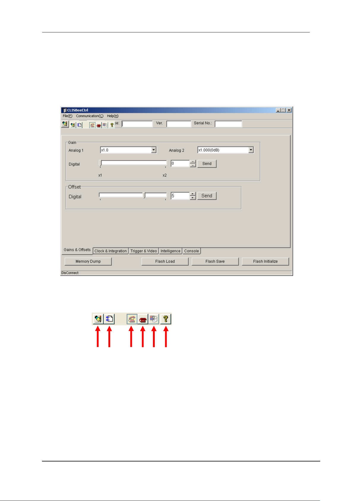
62 NED
A B C D F
E
8.5 Operation
8.5.1 Start Program
Open Windows Explorer and Double-click the “CLISBeeCtrl.exe”.
It is possible to switch the page by clicking each tab under the window.
Buttons in the tool-bar have the following functions.
A: Exporting parameters in the text file format.
B: Load the parameters from a text file (*.txt file)
C: Connection with the camera.
D: Disconnection.
E: Setting Communication.
F: Version Information.
XCM4085TLCT6 UME-0062-01
Page 63
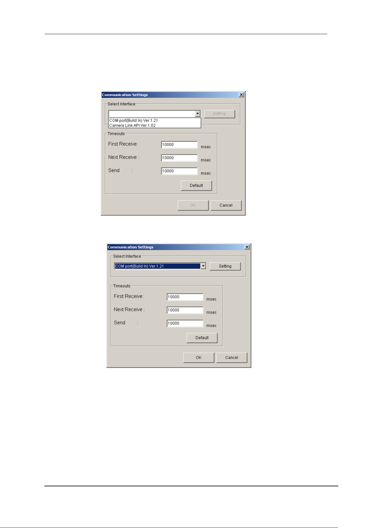
63 NED
8.5.2 Selecting interface and Timeout setting
8.5.2.1 Selecting interface
1) Click button E.
2) Select the interface in Drop-down-list-box.
3) Click “Setting” button to set the interface. (See 8.5.2.2. and 8.5.2.3.)
4) Click “OK” button.
Click “Cancel” button when stopping setup.
Note: The camera can be used without this operation after it has been set up
correctly.
XCM4085TLCT6 UME-0062-01
Page 64
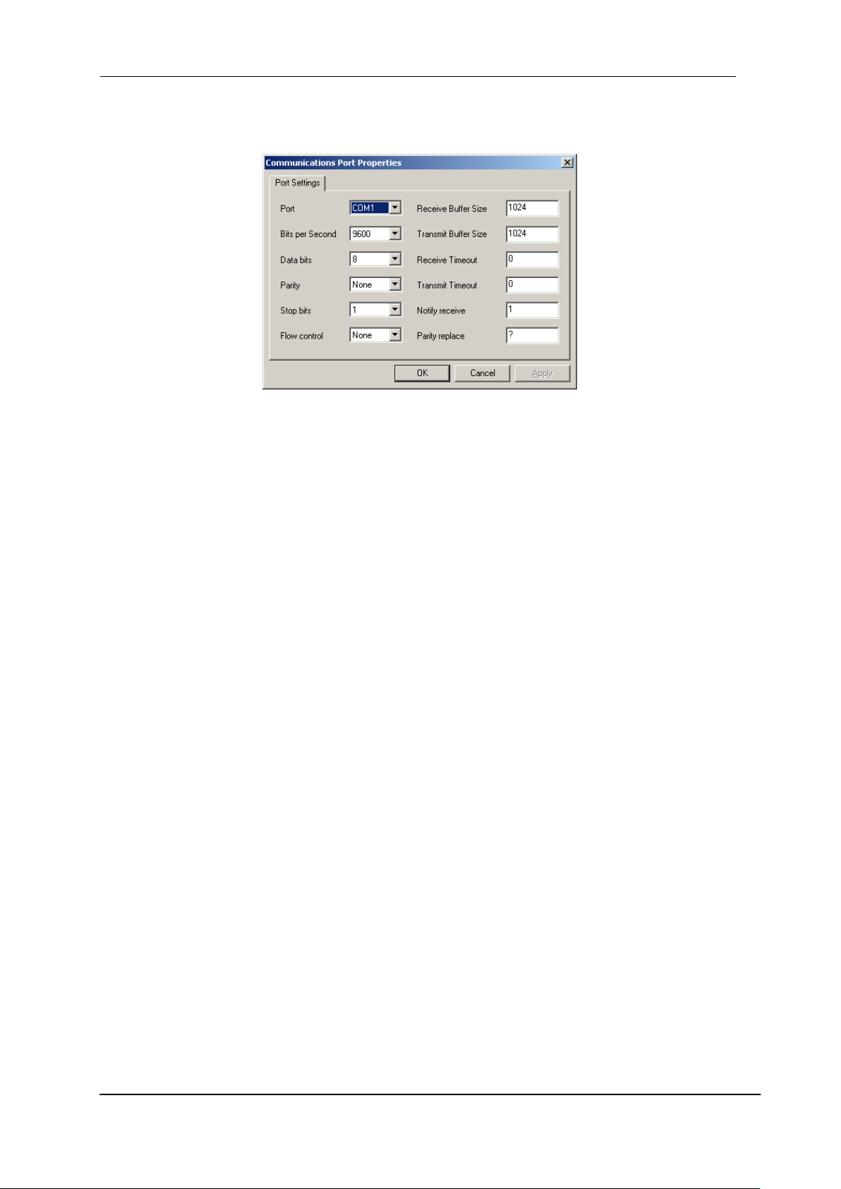
64 NED
8.5.2.2 Setting Communication port
1) Set up each item as follows. (NED standard)
However, when the setup which differs to the camera to connect is shown, follow
there.
(1) Port: Select connecting port.
(2) Bits per Second: 115200
(3) Data bits: 8
(4) Parity: None
(5) Stop bits: 1
(6) Flow control: None
Note: Other parameters are not used.
Click “OK” button.
Click “Cancel” button when stopping setup.
Note:
The camera can be used without this operation after it has been set up correctly.
XCM4085TLCT6 UME-0062-01
Page 65
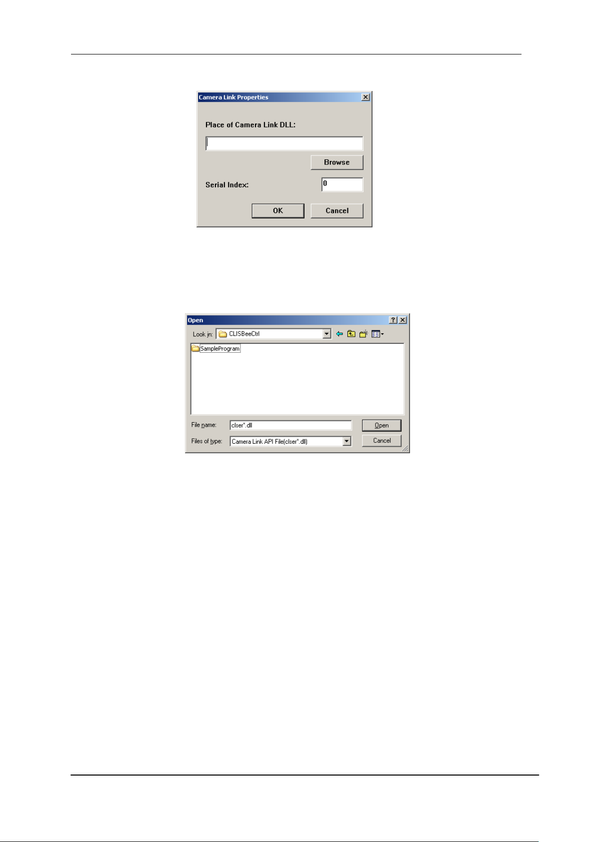
65 NED
8.5.2.3 Setting Camera Link API
Input the DLL file name for Camera Link API by edit-box,
Or click “Browse” button and select this file.
Input value corresponding to the position of Camera Link cable to connect, into
“Serial Index” column.
Click “OK” button.
Click “Cancel” button when stopping setup.
Note: The camera can be used without this operation after it has been set up
correctly.
Note: DLL for Camera Link API is provided by the manufacturer of the grabber
board.
Some frame grabber boards are connected directly to the PC’s COM port, in
this case, select interface to COM port (RS232C). Please contact the
manufacturer of the grabber board for detail.
XCM4085TLCT6 UME-0062-01
Page 66
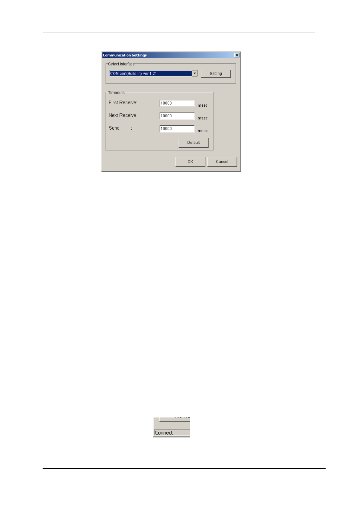
66 NED
8.5.2.4 Setting Timeout
Input each timeout value in the edit-box.(unit :ms)
When you will click on the “Default” button, the value will be reset to the cameras
default values.
The meanings of each timeout are as follows.
First Receive: The maximum time from sending a command to receiving the
first data.
Next Receive: The maximum time between a letter and the next one.
Send: The maximum time until finishing sending a command.
Click “OK” button.
Click “Cancel” button when stopping setup.
Note: The camera can be used without this operation after it has been set up
correctly.
8.5.3. Connect
Click button C. Then you can control the camera. (See “8.6.Control”)
Click the “Memory Dump” button to acquire the current data of the camera.
XCM4085TLCT6 UME-0062-01
Page 67
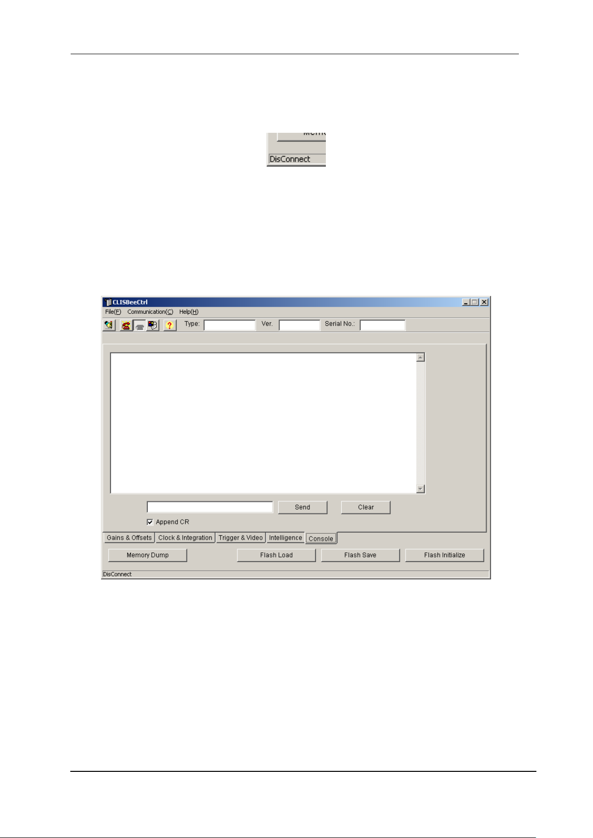
67 NED
8.5.4. Disconnect and end program
Click button D. Then click “X” button in the upper right of the window.
8.5.5. Check of the contents of communication
Click “Console” tag near the bottom window.
XCM4085TLCT6 UME-0062-01
Page 68
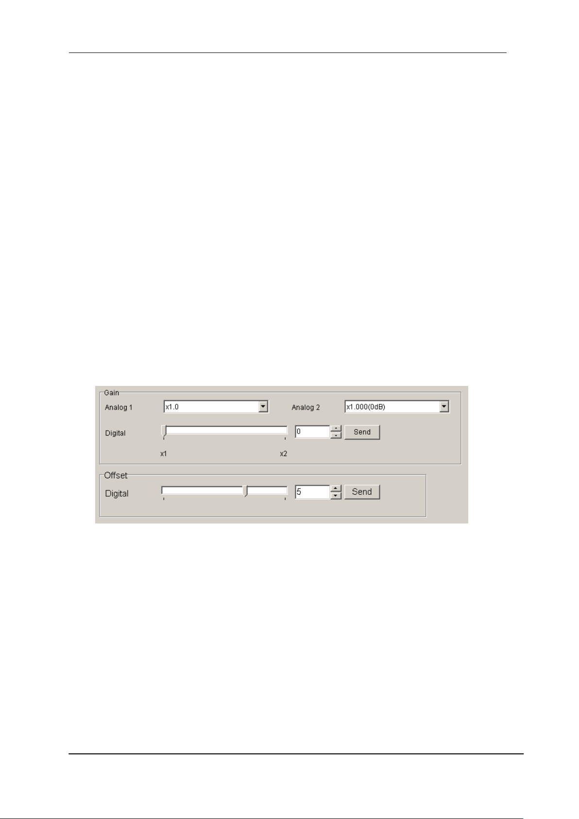
68 NED
8.6 Control
8.6.1 Gains and Offsets
Operating it in『Gains & Offsets』tab.
< Gain >
Analog 1 :
The signal will be sent to the camera every time you make a selection from the
menu in the drop-down-list-box.
Note:
This camera does not use ‘Analog 2’
Digital :
Set a value with the slider, the edit-box or the spin-button. Then, click “Send”
button.
< Offset >
Digital :
Set a value with the slider, the edit-box or the spin-button. Then, click “Send”
button.
XCM4085TLCT6 UME-0062-01
Page 69
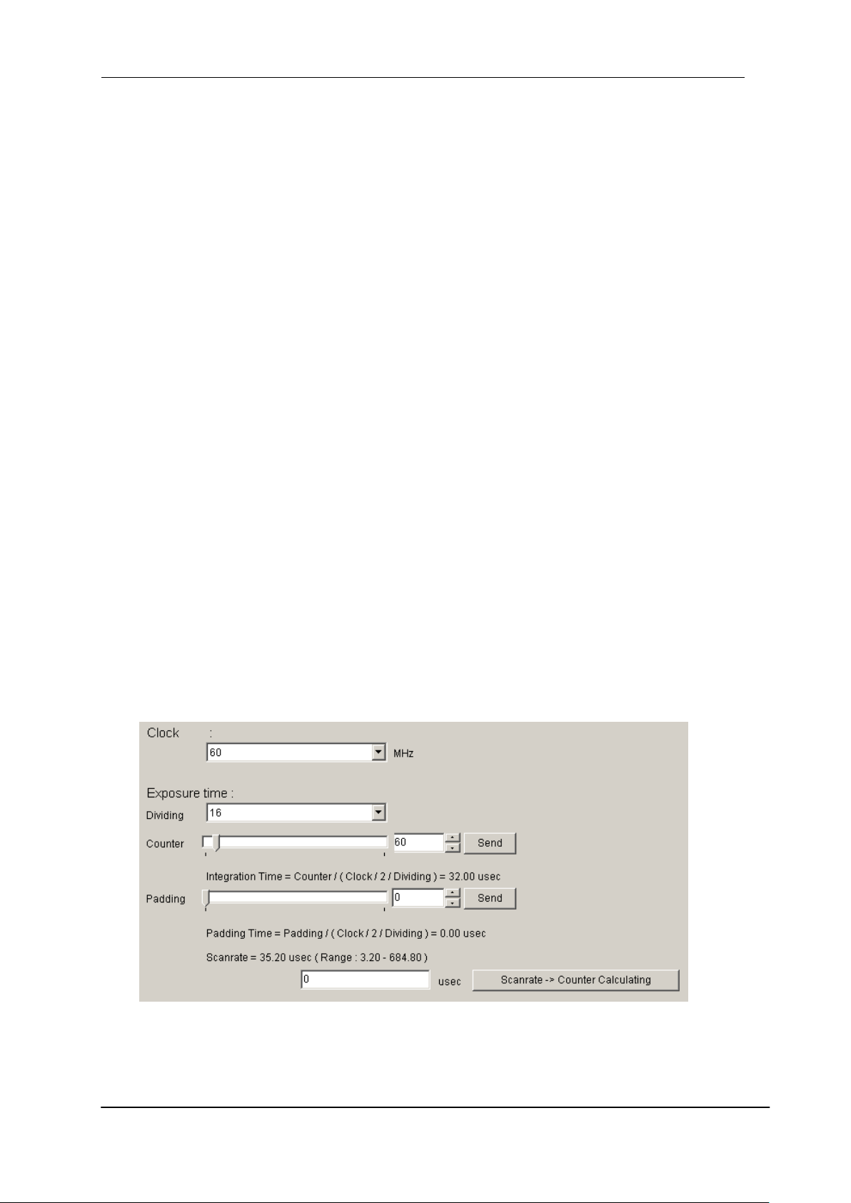
69 NED
8.6.2 Clock & Integration
Operating it in『Clock & Integration』tab.
Clock :
Shows the camera internal clock frequency.
Note: Read Only
Integration Time :
Setting integration time. (Unit: μs) When the trigger mode is Free Run, and Ext
Edge
Dividing / Counter :
First, choose a dividing clock from the drop-down-list-box.
Next, set a counter value with the slider, edit-box or the spin-button. Then, click
“Send” button.
Padding : Read Only
Scanrate -> Counter automatic setting:
The Counter value of Clock, Diving, and Padding is calculated and set from the
present value when the scanning cycle to be set to the edit-box is input and it then
click on the scanrate->counter calculating button.
Note:
The calculating formula and the value at exposure time (Integration Time) are
displayed by the unit of μs.
The calculating formula and the value of PaddingTime are displayed by the unit of
μs.
The calculation value at scanning cycle (Scanrate) is displayed by the unit of μs.
XCM4085TLCT6 UME-0062-01
Page 70
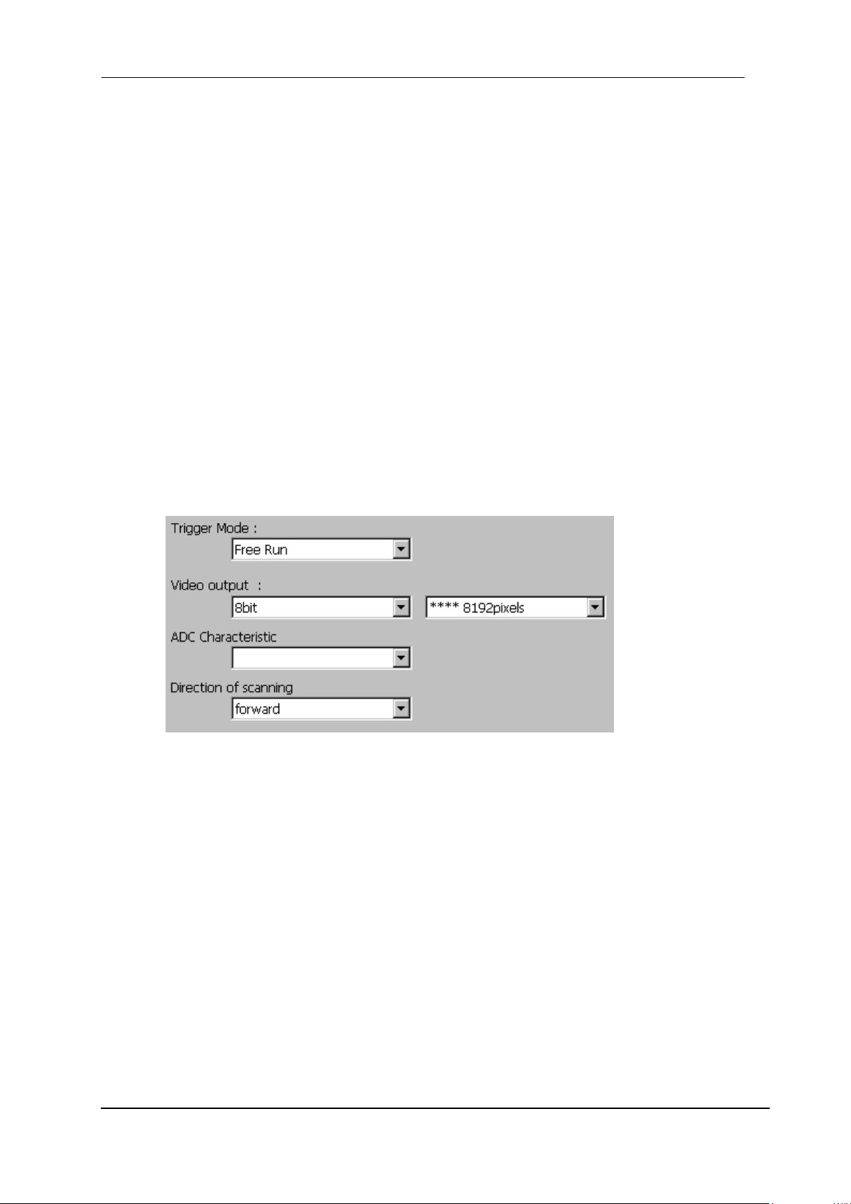
70 NED
l
inear
8.6.3 Exposure mode (Trigger Mode) & Video output mode
Operating it in the『Trigger & Video』tab.
Exposure mode (Trigger Mode) :
Select Free Run Exposure mode, External Trigger Exposure mode and External
Trigger level. The signal will be sent to the camera every time you make a
selection from the menu in the drop-down-list-box.
Video output:
Select the number of the output block. The signal will be sent to the camera every
time you choose make a selection from the menu in the drop-down-list-box.
Direction of scanning:
The order of outputting data from the camera is switched in positive direction
(forward) or opposite direction (reverse).
XCM4085TLCT6 UME-0062-01
Page 71
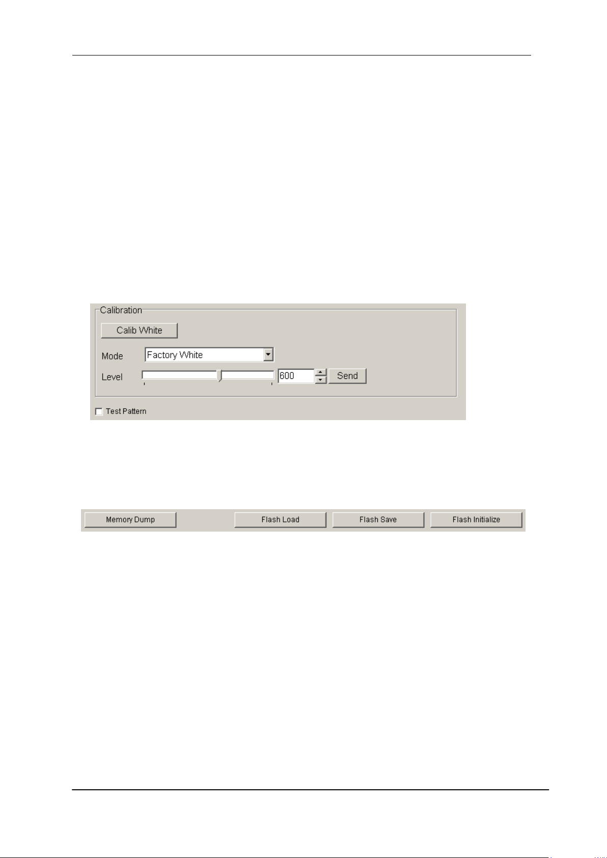
71 NED
8.6.4 Intelligence
Operating it in the『Intelligence』tab.
< Calibration >
Calib White:
Acquisition of white data and saving the calibration data to camera’s flash
memory.
Mode / Level:
First, choose the mode from the drop-down-list-box.
Next, set a value with the slider, the edit-box or the spin-button. Then, click
“Send” button.
Test Pattern:
On/Off of the test pattern output is switched clicking the check box.
8.6.5 Memory in camera
Memory Dump :
Read the data from the camera’s work memory.
Flash Load :
Loading the data from the camera’s flash memory.
Flash Save :
Saving the data in the camera’s flash memory.
Flash Initialize :
Initializing the camera’s flash memory with the factory standard data.
Note:
It takes a while to save and initialize.
XCM4085TLCT6 UME-0062-01
Page 72

72 NED
8.7 Upgrade
When installing a newer / updated software version from our company,
Please perform in the following procedure.
Check the CLISBeeCtrl has not started.
Uninstall the old version software. (See “8.4.Uninstall”)
Install new version software. (See “8.3.Install”)
8.8 How to Program
Please refer sample programs in CLISBeeCtrl¥SampleProgram folder.
8.9 Attention on use
Reproducing and distributing without notice the part or all of this software and this
book is prohibited.
Reverse engineering, decompiling, disassembling and modifying without notice the
part or all of this software is prohibited.
The specification of this software and the contents of this book may be changed
without announcement in future.
XCM4085TLCT6 UME-0062-01
Page 73

73 NED
9 Others
9.1 Notice
No part of this document may be reproduced in any form, in whole or in part,
without the expressed written consent of NED.
Contents of this document are subject to change without prior notice.
Every care has been taken in the preparation of this User’s Manual. If you should
discover any errors or omissions, please notify your nearest NED representative.
9.2 Contact for support
Nippon Electro-Sensory Devices Corporation
Head Office
2-5-12, Itachibori, Nishi-ku, Osaka 550-0012, Japan
Phone +81-6-6534-5300
Fax +81-6-6534-6080
Tokyo Branch
Gibraltar Oi BLDG., Room No.402
1-45-2, Oi, Shinagawa-ku, Tokyo 140-0014, Japan
Phone +81-3-5718-3181
Fax +81-3-5718-0331
Nishi-Nippon Branch
Twin Square 1-8-28 Enokida, Hakata-ku, Fukuoka, 812-0004, Japan
Phone +81-92-451-9333
Fax +81-92-451-9335
URL
http://ned-sensor.co.jp/en/
E-Mail
[email protected]
XCM4085TLCT6 UME-0062-01
Page 74

74 NED
9.3 Product Support
If there is still a problem with your camera after checking it in accordance with the
troubleshooting guide, turn off the power and call your NED representative.
In such case, please inform us of the status of the camera. You can get the status
on console by
(1) executing the “sta” command, or
(2) clicking “Memory Dump” button when using CLISBeeCtrl.
XCM4085TLCT6 UME-0062-01
Page 75
75 NED
Revision
Number
Date
Changes
01
22 October 2015
Initial release
XCM4085TLCT6 UME-0062-01
 Loading...