


DATA SHEET
MOS INTEGRATED CIRCUIT
PD72862
µµµµ
IEEE1394 OHCI HOST CONTROLLER
The µPD72862 is IEEE1394 OHCI-Link controller. The µPD72862 complies with the P1394a draft 2.0
specifications and works up to 400 Mbps.
It supports both of the Cardbus interface and the PCI bus interface.
FEATURES
• Compliant with Link Layer Services as defined in 1394 Open Host Controller Interface specification release 1.0
• Compliant with protocol enhancement as defined in P1394a draft 2.0
• Modular 32-bit host interface compliant to PCI Specification release 2.1
• Supports PCI-Bus Power Management Interface Specification release 1.0
• Supports Cardbus
• Equipped CIS register
• Cycle Master and Isochronous Resource Manager capable
• Compatible to PHY Layer implementation of 100/200/400 Mbps via 2/4/8-bit data interface
• Built-in FIFOs for isochronous transmit (1024 bytes), asynchronous transmit (1024 bytes), and receive (2048
bytes)
• 32-bit CRC generation and checking for receive/transmit packets
• 4-isochronous transmit DMAs and 4-isochronous receive DMAs supported
• Support both IEEE1394-1995 compliant PHY and P1394a compliant PHY
• Internal control and operational registers direct-mapped to PCI configuration space
• 2-wire Serial EEPROMTM interface supported
ORDERING INFORMATION
Part number Package
µ
PD72862GC-9EU 100-pin plastic TQFP (Fine pi tch) (14 x 14)
The information in this document is subject to change without notice. Before using this document, please
confirm that this is the latest version.
Not all devices/types available in every country. Please check with local NEC representative for
availability and additional information.
Document No. S14265EJ2V0DS00 (2nd edition)
Date Published December 1999 NS CP (K)
Printed in Japan
The mark
★★★★
shows major revised points.
1999
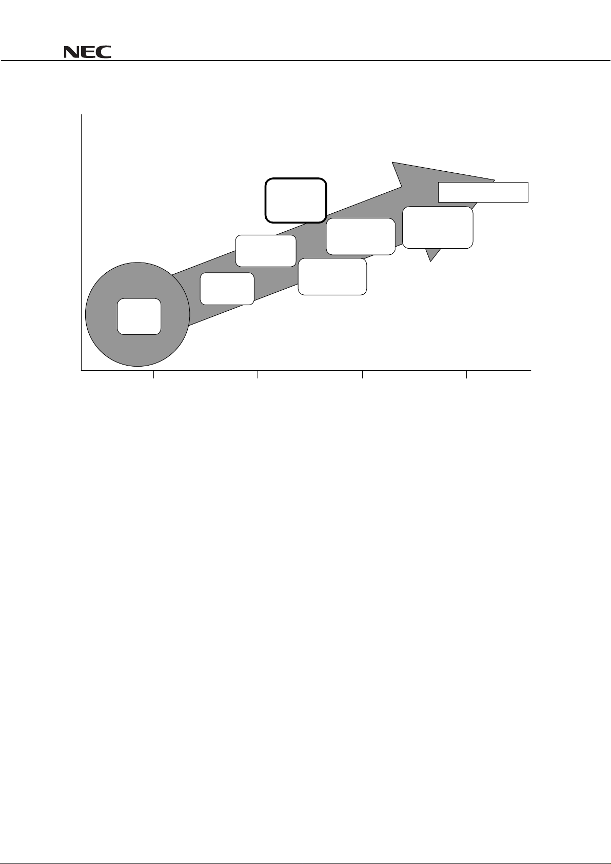
Firewarden™ ROADMAP
µµµµ
Firewarden Series
PD72862
IEEE1394-1995
Core Development
Hotline
Link
1997
OHCI Link
µ
1998
PD72860
OHCI Link
µ
PD72862
OHCI Link
µ
PD72861
1 Chip
OHCI+PHY
µ
PD72870A
1 Chip
OHCI+PHY
µ
PD72870
800M/1.6G
p1394.b Link
µ
PD7286x
1999 2000
PC Application
2001
2
Data Sheet S14265EJ2V0DS00
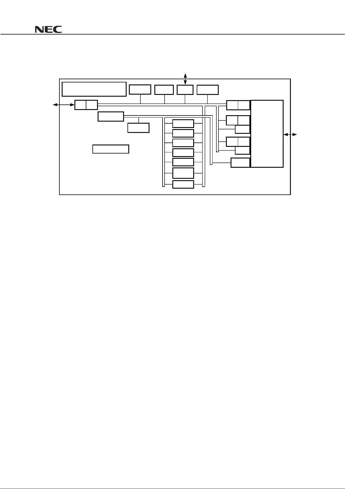
BLOCK DIAGRAM
(
)
Serial ROM Interface
µµµµ
PD72862
PCI Controller Interface
(Master, Parity Check & Generator)
Byte
Buf
Swap
Cardbus Interface
PCI Bus /
OPCIBUS_AR B
PCIS_CNT
PCI-DMA
OPCI Internal Bus
PCIS Bus
PCICFG
IOREG
PCI Slave Bus
IRDMA0-
ATDMA : Asynchronous Transmit DMA
ATF : Asynchronous Transmit FIFO
CIS : CIS Register
CSR : Control and Status Registers
IOREG : IO Registers
IRDMA : Isochronous Receive DMA
ITCF : Isochronous Transmit Control FIFO
ITDMA : Isochronous Transmit DMA
ITF : Isochronous Transmit FIFO
OPCIBUS_ARB : OPCI Internal Bus Arbitration
PAU : Physical Response and Request Unit
PCICFG : PCI Configuration Registers
PCIS_CNT : PHY Control Isochronous Control
PFCOMM : Pre Fetch Command FIFO
RCF : Receive Control FIFO
RF : Receive FIFO
SFIDU : Self-ID DMA
CSR
(CIS)
ATDMA
PAU
GRSU
GRQU
ITDMA
IRDMA3
SFIDU
PFCOMM
Byte
Swap
Byte
Swap
RF
ATF
ITF
ITCF
Byte
Swap
RCF
IOREG
Link Layer
Core
PHY/Link Interface
Data Sheet S14265EJ2V0DS00
3
µµµµ
PD72862
PIN CONFIGURATION (Top View)
Though the current implementation of the µPD72862 includes signal pins for debugging and testing purpose, the
package remains a cost efficient 100-pin TQFP package.
• 100-pin plastic TQFP (Fine pitch) (14 x 14)
DD
3.3V V
AD21
AD20
AD19
AD18
SS
V
AD17
AD16
CBE2
FRAME
DD
PCI V
IRDY
TRDY
DEVSEL
STOP
PERR
SERR
PAR
SS
V
CBE1
AD15
AD14
AD13
AD12
DD
3.3V V
1
2
3
4
5
6
7
8
9
10
11
12
13
14
15
16
17
18
19
20
21
22
23
24
25
SS
V
100
26
AD22
99
28
27
AD23
98
29
DD
IDSEL
3.3V V
96
97
30
CBE3
95
32
31
AD24
94
33
DD
PCI V
AD25
92
93
34
AD26
91
35
AD28
AD27
89
90
37
36
AD29
88
38
AD30
87
39
86
40
VSSAD31
41
85
REQ
84
42
GNT
83
43
PCLK
82
44
INTA
PRST
80
81
46
45
PME
79
47
CLKRUN
77
78
485049
VSSLINKON
76
75
74
73
72
71
70
69
68
67
66
65
64
63
62
61
60
59
58
57
56
55
54
53
52
51
DD
3.3V V
LPS
LREQ
SCLK
SS
V
CTL0
CTL1
DIRECT
D0
D1
D2
D3
SS
V
D4
D5
D6
D7
NC
GROM_EN
GROM_SCL
GROM_SDA
CARD_ON
NC
NC
DD
3.3V V
SS
V
AD10
AD11
4
AD9
AD8
SS
V
AD5
AD6
AD7
CBE0
Data Sheet S14265EJ2V0DS00
AD4
SS
DD
V
PCI V
AD3
AD2
AD1
AD0
IC(H)
PIN_EN
IC(L)
CIS_ON
IC(L)
NC
NC
SS
V

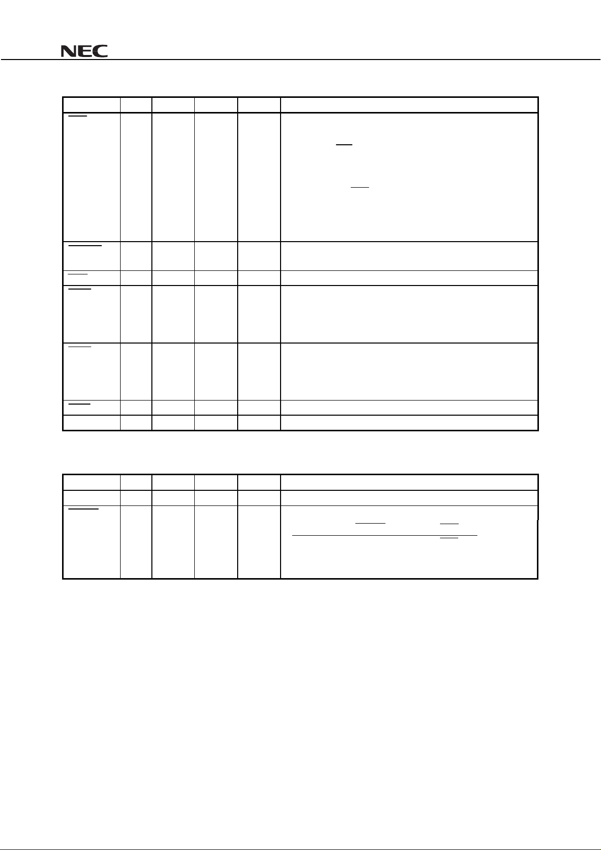
PIN NAME
AD0-AD31 : PCI Multiplexed Address and Data
CARD_ON : PCI/Card Select
CBE0-CBE3 : Command/Byte Enables
CIS_ON : CIS Register ON
CLKRUN : PCICLK Running
CTL0, CTL1 : PHY/Link Bi-directional Control
DEVSEL : Device Select
DIRECT : Auxiliary PHY/Link Signal
D0-D7 : PHY/Link Bi-directional Data
FRAME : Cycle Frame
GNT : Bus_master Grant
GROM_EN : Serial EEPROM Enable
GROM_SCL : Serial EEPROM Clock Output
GROM_SDA : Serial EEPROM Data Input / Output
IC (H) : Internally Connected (High Clamped)
IC (L) : Internally Connected (Low Clamped)
IDSEL : ID Select
INTA : Interrupt
IRDY : Initiator Ready
LINKON : Link-On Request
LPS : Link Power Status
LREQ : PHY/Link Request
NC : Non-Connection
PAR : Parity
PCLK : PCI Clock
PERR : Parity Error
PIN_EN : Pin Enable Input
PME : PME Output
PRST : Reset
REQ : Bus_master Request
SCLK : PHY Clock
SERR : System Error
STOP : PCI Stop
TRDY : Target Ready
V
DD
V
SS
: Supply Voltage
: Ground
µµµµ
PD72862
Data Sheet S14265EJ2V0DS00
5

µµµµ
PD72862
CONTENTS
1. PIN FUNCTIONS.....................................................................................................................................8
1.1 PCI Bus Interface Signals: (52 pins) ..............................................................................................8
1.2 PCI/Cardbus Select Signals: (2 pins).............................................................................................9
1.3 PHY/Link Interface Signals: (15 pins) ..........................................................................................10
1.4 Serial ROM Interface Signals: (3 pins).........................................................................................10
1.5 Miscellaneous Signal: (1 pin) .......................................................................................................10
1.6 IC: (3 pins) ......................................................................................................................................10
1.7 NC: (5 pins).....................................................................................................................................10
DD
1.8 V
1.9 V
: (8 pins)....................................................................................................................................10
SS
: (11 pins).................................................................................................................................. 10
2. REGISTER DESCRIPTIONS.................................................................................................................11
2.1 PCI Bus Mode Configuration Register ( CARD_ON=Low )........................................................ 11
2.1.1 Offset_00 VendorID Register.............................................................................................................12
2.1.2 Offset_02 DeviceID Register..............................................................................................................12
2.1.3 Offset_04 Command Register............................................................................................................12
2.1.4 Offset_06 Status Register..................................................................................................................13
2.1.5 Offset_08 Revision ID Register..........................................................................................................14
2.1.6 Offset_09 Class Code Register..........................................................................................................14
2.1.7 Offset_0C Cache Line Size Register..................................................................................................14
2.1.8 Offset_0D Latency Timer Register.....................................................................................................14
2.1.9 Offset_0E Header Type Register.......................................................................................................14
2.1.10 Offset_0F BIST Register...................................................................................................................14
2.1.11 Offset_10 Base Address 0 Register.................................................................................................15
2.1.12 Offset_2C Subsystem Vendor ID Register.......................................................................................15
2.1.13 Offset_2E Subsystem ID Register....................................................................................................15
2.1.14 Offset_30 Expansion Rom Base Address Register..........................................................................15
2.1.15 Offset_34 Cap_Ptr Register.............................................................................................................15
2.1.16 Offset_3C Interrupt Line Register.....................................................................................................16
2.1.17 Offset_3D Interrupt Pin Register......................................................................................................16
2.1.18 Offset_3E Min_Grant Register.........................................................................................................16
2.1.19 Offset_3F Max Lat Register .............................................................................................................16
2.1.20 Offset_40 PCI_OHCI_Control Register............................................................................................16
2.1.21 Offset_60 Cap_ID & Next_Item_Ptr Register...................................................................................17
2.1.22 Offset_62 Power Management Capabilities Register.......................................................................17
2.1.23 Offset_64 Power Management Control/Status Register...................................................................17
2.2 CardBus Mode Configuration Register ( CARD_ON=High )...................................................... 18
2.2.1 Offset_14/18 Base_Address_1/2 Register (CardBus Status Registers)............................................19
2.2.2 Offset_28 Cardbus CIS Pointer..........................................................................................................20
2.2.3 Offset_80 CIS Area............................................................................................................................20
3. SERIAL ROM INTERFACE.................................................................................................................. 21
3.1 Serial EEPROM Register ............................................................................................................... 21
3.2 Serial EEPROM Register Description ..........................................................................................21
3.3 Load Control................................................................................................................................... 25
3.4 Programming Sequence Example................................................................................................25
6
Data Sheet S14265EJ2V0DS00

µµµµ
PD72862
4. ELECTRICAL SPECIFICATIONS.........................................................................................................27
5. APPLICATION CIRCUIT EXAMPLE....................................................................................................30
6. PACKAGE DRAWING .......................................................................................................................... 31
7. RECOMMENDED SOLDERING CONDITIONS...................................................................................32
Data Sheet S14265EJ2V0DS00
7
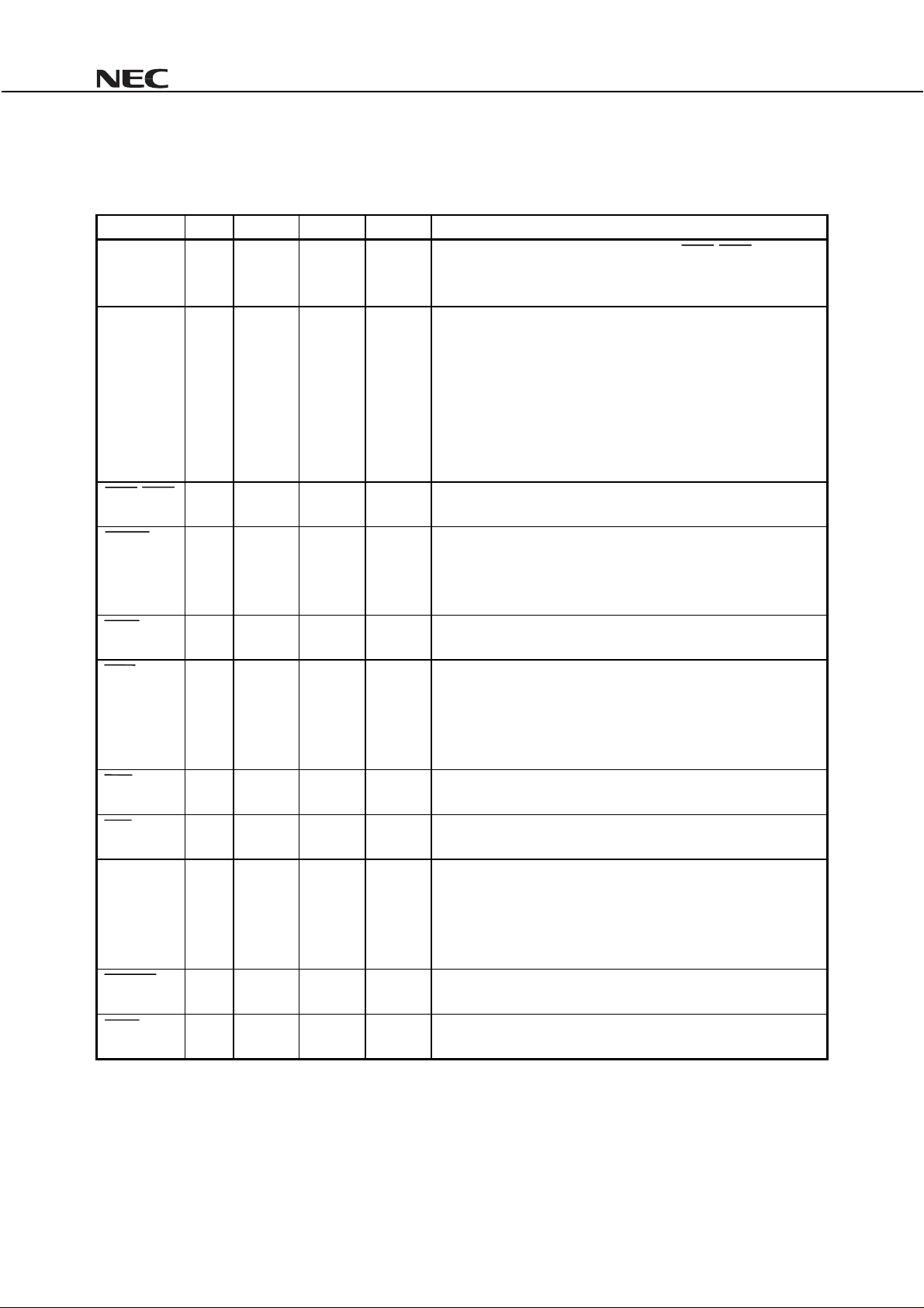
1. PIN FUNCTIONS
1.1 PCI Bus Interface Signals: (52 pins)
Name I/O Pin No. I
PAR I/O 18
AD0-AD31 I/O 2-5, 7, 8,
21-24,
27-30,
33-36,
39-42,
86-91,
93, 94,
98, 99
CBE0-CBE3 I 9, 20,
32, 95
FRAME I/O 10
PCI/Cardbus
PCI/Cardbus
PCI/Cardbus
★★★★
TRDY I/O 13
IRDY I/O 12
REQ O 84
GNT I 83 - 5/3.3
IDSEL I 96 - 5/3.3
PCI/Cardbus
PCI/Cardbus
PCI/Cardbus
★★★★
DEVSEL I/O 14
STOP I/O 15
PCI/Cardbus
PCI/Cardbus
OL
Volts(V) Function
5/3.3
5/3.3
- 5/3.3
5/3.3
5/3.3
5/3.3
5/3.3
5/3.3
5/3.3
µµµµ
PD72862
(1/2)
Parity
is even parity across AD0-AD31 and CBE0-CBE3. It is an
input when AD0-AD31 is an input; it is an output when AD0-AD31 is
an output.
PCI Multiplexed Address and Data
Command/Byte Enabl es
enables.
Cycle Frame
beginning and is kept asserted duri ng the burst cycle.
If Cardbus mode (CARD_ON = 1), this pi n i s should be pulled up to
DD
V
.
Target Ready
transaction is ready t o be completed.
Initiator Ready
complete the current data phas e. During a write, its assertion
indicates that the ini tiator is driving valid dat a onto the data bus.
During a read, its assertion i ndi cates that the initiator is ready to
accept data from the currently-addressed target.
Bus_master Request
wants to become a bus mast er.
Bus_master Grant
has been granted.
ID Select
selected for configurat i on read/write transaction during the phas e of
device initialization.
If Cardbus mode (CARD_ON = 1), this pi n i s should be pulled up to
DD
V
.
Device Select
has decoded its address as the target of the current acc ess.
PCI Stop
requesting the current bus mas ter to stop the transacti on.
is asserted by the initiator to indicate the cycle
indicates that the c urrent data phase of the
indicates that the c urrent bus master is ready to
when actively driven, i ndi cates that the IUHC is chip-
when actively driven, i ndi cates that the driving dev i ce
when actively driven, i ndi cates that the target is
are multiplexed Bus Commands & Byte
indicates to the bus arbiter that this device
indicates to this device that access to the bus
8
Data Sheet S14265EJ2V0DS00
Name I/O Pin No. I
PME O 79
OL
PCI/Cardbus
Volts(V) Function
5/3.3
PME Output
for power management enable.
µµµµ
PD72862
(2/2)
★★★★
CLKRUN I/O 78
INTA O 80
PERR I/O 16
SERR O 17
PRST I 81 - 5/3.3
PCLK I 82 - 5/3.3
PCI/Cardbus
PCI/Cardbus
PCI/Cardbus
PCI/Cardbus
5/3.3
5/3.3
5/3.3
5/3.3
Caution
PCICLK Running
output, to request starting or speeding up clock.
Interrupt
Parity Error
transactions, except a Special Cycle. It is an output when AD0AD31 and PAR are both inputs. It is an input when AD0-AD31 and
PAR are both outputs.
System Error
errors during the Special Cycle, or any other system error where the
effect can be catas t rophi c. When reporting address parity errors , it
is an output.
Reset
PCI Clock
The PME pin is not an N- c ha nne l open drain str uc t ure pin.
Therefore, when using S3, S4, S5 state in ACPI, a
circuit that can separate between the power supply
and the PME pin externally is needed.
ACPI: Advanced Configuration and Power Interface.
Please refer to ACPI Specification.
as input, to determine the status of PCLK; as
the PCI interrupt request A .
is used for reporting data parity errors during all PCI
is used for reporting address parity errors, data parity
PCI reset
33 MHz system bus clock.
1.2 PCI/Cardbus Select Signals: (2 pins)
Name I/O Pin No. I
CARD_ON I 54 - 3.3
CIS_ON I 45 - 3.3
OL
Volts(V) Function
PCI/Card Select
CIS Register ON
CARD_ON CIS_ON CIS PME
(1:Cardbus, 0:PCI bus)
0
0
1
1
0
X
off
on
on
PME
CSTSCHG
CSTSCHG
Data Sheet S14265EJ2V0DS00
9
1.3 PHY/Link Interface Signals: (15 pins)
µµµµ
PD72862
Name I/O Pin No. I
D0-D7 I/O 59-62,
64-67
CTL0,CTL1 I/O 69, 70 9mA 3.3
LREQ O 73 9mA 3.3
LINKON I 77 - 3.3
LPS O 74 9mA 3.3
SCLK I 72 - 3.3
DIRECT I 68 - 3.3
OL
9mA 3.3
Volts(V) Function
1.4 Serial ROM Interface Signals: (3 pins)
Name I/O Pin No. I
GROM_SDA I/O 55 6mA 3.3
GROM_SCL O 56 6mA 3.3
GROM_EN I 57 - 3.3
OL
Volts(V) Function
PHY/Link Bi-directional Data
PHY/Link Bi-directional Control
PHY/Link Request
Link-On Request
Link Power Status
PHY Clock
Auxiliary PHY/Link Signal
interconnection between Link and PHY has isolation (‘low’: I SObarrier; ‘high’: no ISO-barrier).
Serial EEPROM Data Input / Output
Serial EEPROM Clock Output
Serial EEPROM Enable
Load disabled)
(ISO-barrier supported)
(ISO-barrier supported)
(ISO-barrier supported)
49.152 MHz (ISO-barrier supported)
(ISO-barrier supported)
(ISO-barrier supported)
is used to determine whether the
(‘high’: GUID Load enabled; ‘low’: GUID
1.5 Miscellaneous Signal: (1 pin)
Name I/O Pin No. I
PIN_EN I 43 - 5/3.3
OL
Volts(V) Function
1.6 IC: (3 pins)
Name I/O Pin No. I
IC(H) I 44 - 3.3
IC(L) I 46, 47 - 3.3
OL
Volts(V) Function
1.7 NC: (5 pins)
Name I/O Pin No. I
NC - 48, 49,
52, 53,
58
OL
Volts(V) Function
--
1.8 VDD: (8 pins)
VDD (5 V PCI or 3.3 V PCI) for PCI I/Os: 11, 37, 92
VDD 3 V for digital core & PHY/Link I/Os: 1, 25, 51, 75, 97
Pin Enable Input
Internally Connected
Internally Connected
Non- Connection
Leave them unconnected.
(High clamped)
(High clamped)
(Low clamped)
(Open)
1.9 VSS: (11 pins)
VSS : 6, 19, 26, 31, 38, 50, 63, 71, 76, 85, 100
10
Data Sheet S14265EJ2V0DS00
2. REGISTER DESCRIPTIONS
2.1 PCI Bus Mode Configuration Register ( CARD_ON=Low )
µµµµ
PD72862
31 24 23 16 15 08 07 00
DeviceID VendorID
Status Command
Class Code Revision ID
BIST Header Type Latency Timer Cache Line Size
Base Address 0 (OHCI Regis ters)
Base Address 1
Base Address 2
Base Address 3
Base Address 4
Base Address 5
CardBus CIS Pointer
Subsystem ID Subsystem Vendor ID
Expansion Rom Base Addres s Register
000000H Cap_Ptr
00000000H
Max_Lat Min_Gnt Interrupt Pin Interrupt Line
PCI_OHCI_Control
00000000H
00000000H
00000000H
Diagnostic register0
Diagnostic register1
Diagnostic register2
Diagnostic register3
Power Management Capabilities Next_It em_P t r Cap_ID
Data PMCSR_BSE Power Management Control/Status
00000000H
00000000H
User Area (GENERAL_RegisterA)
User Area (GENERAL_RegisterB)
User Area (GENERAL_RegisterC)
User Area (GENERAL_RegisterD)
00000000H
00H
04H
08H
0CH
10H
14H
18H
1CH
20H
24H
28H
2CH
30H
34H
38H
3CH
40H
44H
48H
4CH
50H
54H
58H
5CH
60H
64H
68H
6CH
70H
74H
78H
7CH
80H
FCH
Data Sheet S14265EJ2V0DS00
11

2.1.1 Offset_00 VendorID Register
This register identifies the manufacturer of the
Bits R/W Description
15-0 R Constant value of 1033H.
PD72862. The ID is assigned by the PCI_SIG committee.
µ
2.1.2 Offset_02 DeviceID Register
This register identifies the type of the device for the
Bits R/W Description
15-0 R Constant value of 0063H.
PD72862. The ID is assigned by NEC Corporation.
µ
2.1.3 Offset_04 Command Register
The register provides control over the device’s ability to generate and respond to PCI cycles.
Bits R/W Description
µµµµ
PD72862
0R
1R/W
2R/W
3R
4R/W
5R
6R/W
7R
8R/W
9R
15-10 R
I/O enable
Memory enable
accesses. This bi t should be set to one upon power-up reset.
Master enable
Special cycle monitor enable
disabled.
Memory write and invalidate enable
Command generation.
VGA color palette invalidate enable
always disabled.
Parity error response
Stepping enable
System error enable
Fast back-to-back enable
allowed to the same agent.
Reserved
Constant value of 0. The µPD72862 does not respond to PCI I/ O accesses.
µ
0: The
1: The
0: The
1: The
0: Memory write must be used
1: The
0: Ignore parity error
1: Respond to parity error
0: Disable system error checking
1: Enable system error checking
PD72862 does not respond to PCI memory cycles
µ
PD72862 responds to PCI memory cycles
µ
PD72862 cannot generate PCI acces ses by being a bus-master
µ
PD72862 is capable of acting as a bus-master
µ
PD72862, when acts as PCI m aster, can generate the command
Constant value of 000000.
Default value of 1. It def i nes if the µPD72862 responds to PCI memory
Default value of 1. It enabl es the µPD72862 as bus-master on the PCI -bus .
Constant value of 0. The special cycle monitor is always
Default value of 0. It enabl es Memory Write and Invalid
Constant value of 0. VGA color palette invalidate is
Default value of 0. It def i nes if the µPD72862 responds to PERR.
Constant value of 0. St eppi ng i s always disabled.
Default value of 0. It def i nes if the µPD72862 responds to SERR.
Constant value of 0. Fast back-to-back transactions are only
12
Data Sheet S14265EJ2V0DS00

2.1.4 Offset_06 Status Register
This register tracks the status information of PCI-bus related events which are relevant to the
and “Write” are handled somewhat differently.
Bits R/W Description
µµµµ
PD72862
PD72862. “Read”
µ
3-0 R
4R
6,5 R
7R
8R/W
10,9 R
11 R/W
12 R/W
13 R/W
14 R/W
15 R/W
Reserved
New capabilities
Reserved
Fast back-to-back capable
cannot accept fast back-to-back transacti ons when the transactions are not to the same agent.
Signaled parity error
DEVSEL timing
Signaled target abort
terminates a transact i on wi th “Target Abort”.
Received target abort
transaction is termi nated with a “Target Abort”.
Received master abort
transaction is termi nated with “Master Abort”. The
transaction response exceeds the time allocated i n t he l atency timer field.
Signaled system error
µ
PD72862.
Received parity error
Constant value of 0000.
Constant value of 00.
0: No parity detected (defaul t )
1: Parity detected
0: Fast (1 cycles)
1: Medium (2 cycles)
2: Slow (3 cycles)
3: undefined
µ
0: The
1: The
0: The
1: The
0: Transaction was not term i nated with a Master Abort
1: Transaction has been terminated with a Master Abort
0: System error was not signaled
1: System error was si gnal ed
0: No parity error was detected
1: Parity error was detect ed
PD72862 did not terminate a transac tion with Target Abort
µ
PD72862 has terminated a transaction with Target Abort
µ
PD72862 has not received a Target Abort
µ
PD72862 has received a Target Abort f rom a bus-master
Constant value of 1. It indic at es the existence of the Capabilities Lis t.
Constant value of 1. It i ndi cates that the µPD72862, as a target,
Default value of 0. It i ndi c ates the occurrence of any “Dat a Parity”.
Constant value of 01. These bits define the decode timing for DEVSEL.
Default value of 0. This bi t is set by a target devi ce whenever it
Default value of 0. This bi t is set by a master dev i ce whenever its
Default value of 0. This bi t is set by a master dev i ce whenever its
µ
PD72862 asserts “Master A bort” when a
Default value of 0. It i ndi c ates that the assertion of SERR by the
Default value of 0. It i ndi c ates the occurrence of any P E RR.
Data Sheet S14265EJ2V0DS00
13

µµµµ
PD72862
2.1.5 Offset_08 Revision ID Register
This register specifies a revision number assigned by NEC Corporation for the
Bits R/W Description
7-0 R Default value of 02H. It spec if ies the silicon revision. It will be incremented for subsequent
silicon revisions.
PD72862.
µ
2.1.6 Offset_09 Class Code Register
This register identifies the class code, sub-class code, and programming interface of the
Bits R/W Description
7-0 R Constant value of 10H. It specifies an I E EE1394 OpenHCI-compliant Host Controller.
15-8 R Constant value of 00H. It specifies an “IEEE 1394” t ype.
23-16 R Constant value of 0CH. It specifies a “Serial B us Controller”.
PD72862.
µ
2.1.7 Offset_0C Cache Line Size Register
This register specifies the system cache line size, which is PC-host system dependent, in units of 32-bit words.
The following cache line sizes are supported: 2, 4, 8, 16, 32, 64, and 128. All other values will be recognized as 0,
i.e. cache disabled.
Bits R/W Description
7-0 R/W Default value of 00H.
2.1.8 Offset_0D Latency Timer Register
This register defines the maximum amount of time that the
PD72862 is permitted to retain ownership of the bus
µ
after it has acquired bus ownership and initiated a subsequent transaction.
Bits R/W Description
7-0 R/W Default value of 00H. It specifies the number of PCI-bus clocks that the µPD72862 may hold
the PCI bus as a bus-mast er.
2.1.9 Offset_0E Header Type Register
Bits R/W Description
7-0 R Constant value of 00H.
It specifies a s i ngl e function device.
2.1.10 Offset_0F BIST Register
Bits R/W Description
7-0 R Constant value of 00H. It specifies whet her the device is capable of Bui l t-in Self Test.
14
Data Sheet S14265EJ2V0DS00

µµµµ
PD72862
2.1.11 Offset_10 Base Address 0 Register
This register specifies the base memory address for accessing all the “Operation registers” (i.e. control,
configuration, and status registers) of the
PD72862, while the BIOS is expected to set this value during power-up
µ
reset.
Bits R/W Description
11-0 R Constant value of 000H. These bi ts are “read-only”.
31-12 R/W -
2.1.12 Offset_2C Subsystem Vendor ID Register
This register identifies the subsystem that contains the NEC’s
PD72862 function. While the ID is assigned by the
µ
PCI_SIG committee, the value should be loaded into the register from the external serial EEPROM after power-up
reset. Access to this register through PCI-bus is prohibited.
Bits R/W Description
15-0 R
Default value of 1033H.
2.1.13 Offset_2E Subsystem ID Register
This register identifies the type of the subsystem that contains the NEC’s
PD72862 function. While the ID is
µ
assigned by the manufacturer, the value should be loaded into the register from the external serial EEPROM after
power-up reset. Access to this register through PCI-bus is prohibited.
Bits R/W Description
15-0 R
Default value of 0063H.
2.1.14 Offset_30 Expansion Rom Base Address Register
This register is not supported by the current implementation of the
Bits R/W Description
31-0 R
Reserved
Constant value of 0.
PD72862.
µ
2.1.15 Offset_34 Cap_Ptr Register
This register points to a linked list of additional capabilities specific to the
PD72862, the NEC’s implementation of
µ
the 1394 OpenHCI specification.
Bits R/W Description
7-0 R Constant value of 60H. The val ue represents an offset into the µPD72862’s PCI Configuration
Space for the location of the f i rs t item in the New Capabilities Linked List.
Data Sheet S14265EJ2V0DS00
15

µµµµ
PD72862
2.1.16 Offset_3C Interrupt Line Register
This register provides the interrupt line routing information specific to the
PD72862, the NEC’s implementation of
µ
the 1394 OpenHCI specification.
Bits R/W Description
7-0 R/W Default value of 00H. It specif i es which input of the host system interrupt controller the
interrupt pin of the
µ
PD72862 is connected to.
2.1.17 Offset_3D Interrupt Pin Register
This register provides the interrupt line routing information specific to the
PD72862, the NEC’s implementation of
µ
the 1394 OpenHCI specification.
Bits R/W Description
7-0 R Constant value of 01H. It specifies PCI INTA is used for interrupting the host system.
2.1.18 Offset_3E Min_Grant Register
This register specifies how long of a burst period the
PD72862 needs, assuming a clock rate of 33MHz.
µ
Resolution is in units of ¼ µs. The value should be loaded into the register from the external serial EEPROM upon
power-up reset, and access to this register through PCI-bus is prohibited.
Bits R/W Description
7-0 R Default value of 00H. Its v al ue contributes to the desired s et ting for Latency Timer value.
2.1.19 Offset_3F Max Lat Register
This register specifies how often the
PD72862 needs to gain access to the PCI-bus, assuming a clock rate of
µ
33MHz. Resolution is in units of ¼ µs. The value should be loaded into the register from the external serial
EEPROM after hardware reset, and access to this register through PCI-bus is prohibited.
Bits R/W Description
7-0 R Default value of 00H. Its v al ue contributes to the desired s et ting for Latency Timer value.
2.1.20 Offset_40 PCI_OHCI_Control Register
This register specifies the control bits that are IEEE1394 OpenHCI specific. Vendor options are not allowed in this
register. It is reserved for OpenHCI use only.
Bits R/W Description
0R/W
31-1 R
PCI global SWAP
the PCI Interface are byte swapped, thus a “PCI Global Swap”. PCI addresses for expansion
ROM and PCI Configuration regist ers , are, however, unaffected by t hi s bit. This bit is not
required for motherboard implementati ons.
Reserved
Default value of 0. When this bit is 1, all quadrates read f rom and wri tten to
Constant value of all 0.
16
Data Sheet S14265EJ2V0DS00

µµµµ
PD72862
2.1.21 Offset_60 Cap_ID & Next_Item_Ptr Register
The Cap_ID signals that this item in the Linked List is the registers defined for PCI Power Management, while the
Next_Item_Ptr describes the location of the next item in the
Bits R/W Description
PD72862’s Capability List.
µ
7-0 R
15-8 R
Cap_ID
Constant value of 01H. The defaul t value identified the Link List item as being the PCI
Power Management registers, whi l e the ID value is assigned by the PCI SIG.
Next_Item_Ptr
List.
Constant value of 00H. It i ndi cated that there are no more items i n t he Li nk
2.1.22 Offset_62 Power Management Capabilities Register
This is a 16-bit read-only register that provides information on the power management capabilities of the
PD72862.
µ
Bits R/W Description
2-0 R
3R
4R
5R
8,6 R
9R
10 R
15-11 R
version
Constant value of 001. The power management registers are implemented as defined
in revision 1.0 of PCI B us Power Management Interface S pec i fication.
PME clock
Auxiliary power source
DIS
Reserved
D1_support
Management state.
D2_support
PME_support
Constant value of 0.
Constant value of 0. The alt ernat i ve power source is not supported.
Constant value of 0.
Constant value of 000.
Constant value of 0. The µPD72862 does not support the D1 Power
Constant value of 1. The µPD72862 supports the D2 Power Management state.
Constant value of 01100.
2.1.23 Offset_64 Power Management Control/Status Register
This is a 16-bit read-only register that provides control status information of the
Bits R/W Description
1,0 R/W
7-2 R
8R/W
12-9 R
14,13 R
15 R/W
PowerState
state of the
supported in the current implem ent ation of the
00: D0 (DMA contexts: ON, Link Layer: ON)
01: Reserved (D1 state not s upport ed)
10: D2 (DMA contexts: OFF, Link Lay er: OFF, LPS: OFF, PME will be asserted upon
11: D3 (DMA contexts: OFF, Link Lay er: OFF, LPS: OFF, PME will be asserted upon
Reserved
PME_En
features of the
Data_Select
Data_Scale
PME_Status
ignored.
Default value is undefined. Thi s field is used both to determ i ne the current power
µ
PD72862 and to set the µPD72862 into a new power state. As D1 i s not
µ
PD72862, writing of ‘01’ will be ignored.
LinkON being active)
LinkON being active, Power can be removed)
Constant value of 000000.
Default value of 0. This field is used to enable the spec i fic power management
µ
PD72862.
Constant value of 0000.
Constant value of 00.
Default value is undefined. A write of ‘1’ clears this bit, while a write of ‘0’ is
PD72862.
µ
Data Sheet S14265EJ2V0DS00
17

2.2 CardBus Mode Configuration Register ( CARD_ON=High )
µµµµ
PD72862
31 24 23 16 15 08 07 00
DeviceID VendorID
Status Command
Class Code Revision ID
BIST Header Type Latency Tim er Cache Line Size
Base Address 0 (OHCI Regis ters)
Base Address 1 (CardBus Status Reg)
Base Address 2 (CardBus Status Reg)
Base Address 3
Base Address 4
Base Address 5
CardBus CIS Pointer
Subsystem ID Subsystem Vendor ID
Expansion Rom Base Addres s Register
000000H Cap_Ptr
Max_Lat Min_Gnt Interrupt Pin Interrupt Line
PCI_OHCI_Control
Diagnostic register0
Diagnostic register1
Diagnostic register2
Diagnostic register3
Power Management Capabilities Next_It em_P t r Cap_ID
Data PMCSR_BSE Power Management Control/Status
User Area (GENERAL_RegisterA)
User Area (GENERAL_RegisterB)
User Area (GENERAL_RegisterC)
User Area (GENERAL_RegisterD)
CIS Area
Different from PCI Bus Mode Configuration Register.
Note
Note
00000000H
00000000H
00000000H
00000000H
00000000H
00000000H
Note
Note
Note
00H
04H
08H
0CH
10H
14H
18H
1CH
20H
24H
28H
2CH
30H
34H
38H
3CH
40H
44H
48H
4CH
50H
54H
58H
5CH
60H
64H
68H
6CH
70H
74H
78H
7CH
80H
FCH
18
Data Sheet S14265EJ2V0DS00

2.2.1 Offset_14/18 Base_Address_1/2 Register (CardBus Status Registers)
Bits R/W Description
7-0 R Constant value of 00.
31-8 R/W -
(1) Function Event Register (FER) ( Base Address 1 ( 2 )+ 0H )
Bits R/W Description
0 R Wri te Protect (No Use).
Read only as ‘0’
1 R Ready Status (No Use).
Read only as ‘0’
2 R B attery Voltage Detect 2 (No Use).
Read only as ‘0’
3 R B attery Voltage Detect 1 (No Use).
Read only as ‘0’
4 R/W General Wakeup
14-5 R Reserved. Read only as ‘0’
15 R/W Interrupt
31-16 R Reserved. Read only as ‘0’
µµµµ
PD72862
(2) Function Event Mask Register (FEMR) ( Base Address 1 ( 2 )+ 4H )
Bits R/W Description
0 R Wri te Protect (No Use).
Read only as ‘0’
1 R Ready Status (No Use).
Read only as ‘0’
2 R B attery Voltage Detect 2 (No Use).
Read only as ‘0’
3 R B attery Voltage Detect 1 (No Use).
Read only as ‘0’
4 R/W General Wakeup Mask
5 R B A M . Read only as ‘0’
6 R P WM . Read only as ‘0’
13-7 R Reserved. Read only as ‘0’
14 R/W Wak eup M ask
15 R/W Interrupt
31-16 R Reserved. Read only as ‘0’
Data Sheet S14265EJ2V0DS00
19

(3) Function Reset Status Register (FRSR) ( Base Address 1 ( 2 )+ 8H )
Bits R/W Description
0 R Wri te Protect (No Use).
Read only as ‘0’
1 R Ready Status (No Use).
Read only as ‘0’
2 R B attery Voltage Detect 2 (No Use).
Read only as ‘0’
3 R B attery Voltage Detect 1 (No Use).
Read only as ‘0’
4 R/W General Wakeup Mask
14-5 R Reserved. Read only as ‘0’
15 R/W Interrupt
31-16 R Reserved. Read only as ‘0’
(4) Function Force Event Register (FFER) ( Base Address 1 ( 2 )+ CH )
µµµµ
PD72862
Bits R/W Description
0 R Wri te Protect (No Use).
Read only as ‘0’
1 R Ready Status (No Use).
Read only as ‘0’
2 R B attery Voltage Detect 2 (No Use).
Read only as ‘0’
3 R B attery Voltage Detect 1 (No Use).
Read only as ‘0’
4 R/W General Wakeup Mask
14-5 - No Use
15 R/W Interrupt
31-16 R Reserved. Read only as ‘0’
2.2.2 Offset_28 Cardbus CIS Pointer
This register specifies start memory address of the Cardbus CIS Area.
Bits R/W Description
31-0 R Starting Pointer of CIS Area.
Constant value of 00000080H.
2.2.3 Offset_80 CIS Area
PD72862 supports external Serial ROM(AT24C02 compatible) interface.
The
µ
CIS Area Register can be loaded from external Serial ROM in the CIS area when CARD_ON are HIGH.
CARD_ON CIS_ON Bus CIS FUNCTION
0 1 PCI OFF PME
0 0 PCI ON CSTSCHG
1 X Cardbus ON CSTSCHG
20
Data Sheet S14265EJ2V0DS00

µµµµ
PD72862
3. SERIAL ROM INTERFACE
The µPD72862 provides a serial ROM interface to initialize the 1394 Global Unique ID Register and the
PCI/Cardbus Mode Configuration registers from a serial EEPROM.
3.1 Serial EEPROM Register
Register Address Register Name R/W
Base address + 0x930 SUBID register R/W
Base address + 0x934 LATVAL register R/W
Base address + 0x938 W_GUIDHi register R/W
Base address + 0x93C W_GUIDLo register R/W
Base address + 0x940 Parameters Write regist er R/W
Base address + 0x95C W_GENERAL register R/W
Base address + 0x960 W_PHYS register R/W
Base address + 0x984 W_CIS register R/W
Remark
Base address : Base Address 0 in Configuration register
3.2 Serial EEPROM Register Description
(1) SUBID register (Base address + 0x930)
31 16 15 0
W_SUBSYSID W_SUBVNDID
Field Bits R/ W Default value Description
W_SUBSYSID 31-16 R/W 0063H Subsystem ID value. The value is loaded into Subsystem ID register in
Configuration register (offset+2CH bit 31-16).
W_SUBVNDID 15-0 R/W 1033H Sub system Vendor ID v al ue. The value is loaded into Subsystem Vendor ID
register in Configuration register (Offset+2CH bit 15-0).
(2) LATVAL register (Base address + 0x934)
31 24 23 16 15 12 11 10 4 3 0
W_MAXLAT W_MINGNT - 0 - 1 - 0 - W_MAX_REC
Field Bits R/ W Default value Description
W_MAXLAT 31-24 R/W 00H Max Latenc y value. The value is loaded into M ax Latency register in
Configuration register (Offset+3CH bit 31-24).
W_MINGNT 23-16 R/W 00H Min Grant value. The value is loaded into Min Grant register in Configurati on
register (Offset+3CH bit 23-16).
-
W_MAX_REC 3-0 R/W 9H MAX__REC value. The value is loaded i nt o the max_rec field of OHCI
15-12 - - Reserved. Writ e 0 to these bits.
11 - - Reserved. Write 1 to this bit.
10-4 - - Reserved. Writ e 0 to these bits.
BusOption register in OHCI regi ster (Offset+020H bit 15-12).
Data Sheet S14265EJ2V0DS00
21

µµµµ
PD72862
(3) W_GUIDHi register (Base address + 0x938)
31 0
W_GUIDHi
Field Bits R/ W Default value Description
W_GUIDHi 31-0 R/W Undefined GlobalUniqueIDHi value. The value is loaded int o OHCI Gl obal Uni queIDHi
register in OHCI register (Offset+024H bit 31-0).
Please refer to the 1394 Open Host Cont rol l er Interface Specific at i on/Release
1.0 [5.5.5].
(4) W_GUIDLo register (Base address + 0x93C)
31 0
W_GUIDLo
Field Bits R/ W Default value Description
W_GUIDLo 31-0 R/ W Undefined Gl obal Uni queI DLo value. The value is loaded into Global Uni queIDLo register
in OHCI register (Offset +028H bi t 31-0).
Please refer to the 1394 Open Host Cont rol l er Interface Specific at i on/Release
1.0 [5.5.5].
(5) Parameters Write register (Base address + 0x940)
31 76 43 10
- 0 - PAGE_S - 0 -
Field Bits R/ W Default value Description
- 31-7 - - Reserved. Writ e 0 to these bits.
PAGE_S 6-4 R/W 000 Write register select page. The bit field returns zero when read.
000: Select SUBID register and LATVAL register.
001: Select W_GUIDHi register and W_GUIDLo register.
010: Select W_GENERAL regis ter (W_GENERAL_0 and W_GENERAL_1).
011: Select W_GENERAL regis ter (W_GENERAL_2 and W_GENERAL_3).
100: Select W_PHYS register (W_ programPhyEnable,
W_aPhyEnhanceEnable).
101: Select W_CIS register (W_CIS_EVEN - W_CIS_ODD).
- 3-1 - - Reserved. Write 0 to these bit s.
PAR_W 0 R/W 0 Writ e control signal. The bit fi el d ret urns zeros when read.
1: Write the value of select page defined PAGE_S. One write transaction is
the units of 8 byte.
0: Ignored.
PAR
_W
22
Data Sheet S14265EJ2V0DS00

µµµµ
PD72862
(6) W_GENERAL register (Base address + 0x950 - 0x95C)
31 0
W_GENERAL_0 (Base address + 0x950) - W_GE NE RA L_3 (Base address + 0x95C)
Field Bits R/ W Default value Description
W_GENERAL_0 W_GENERAL_3
31-0 R/W Undefined User define value. The value is l oaded i nto GENERAL_registerA - D in
Configuration register (Offset+70H - 7BH).
(7) W_PHYS register (Base address + 0x960)
31 10 9 8 7 3 2 0
- 0 - - 0 - - 1 W_aPhyEnhanceEnable
W_programPhyEnable
Field Bits R/ W Default value Description
- 31-10 - - Reserved. Write 0 to these bits.
W_programPhyEnable
W_aPhyEnhanceEnable
9 R/W 1 programPhyEnabl e bi t. The bit is loaded into HCControl regi sters in OHCI
register ((Offset+50H bit 23) and (54H bi t 23)).
Please refer to the 1394 Open Host Cont rol l er Interface Specific at i on/Release
1.0 [5.7].
1: P1394a enhancement is support ed.
0. P1394a enhancement is not s upported.
8 R/W 0 aPhyEnhanc eE nabl e bi t. The bit is loaded into HCControl regi sters in OHCI
register ((Offset+50H bit 23) and (54H bi t 23)).
7-3 - - Reserved. Write 0 to these bits.2-0 - - Reserved. Write 1 to these bits.
(8) W_CIS register (Base address + 0x980 - 0x984)
31 0
W_CIS_EVEN (Base address + 0x980) - W_CIS_ODD (Base addres s + 0x984)
Field Bits R/ W Default value Description
W_CIS_EVEN W_CIS_ODD
31-0 R/W Undefined CIS Area value. The value is l oaded i nto CIS Area in Configuration register
(Offset+80H - FCH).
Data Sheet S14265EJ2V0DS00
23

Table 3-1. Serial EEPROM Memory Map
µµµµ
PD72862
Byte
address
0 W_SUBSYSID(31 : 24)
1 W_SUBSYSID(23 : 16)
2 W_SUBVNDID(15 : 8)
3 W_SUBVNDID( 7 : 0)
4 W_MAXLAT(31 : 24)
5 W_MINGNT(23 : 16)
600001000
7 0 0 0 0 W_MAX_REC( 3 : 0)
8 W_GUIDHi(31 : 24)
9 W_GUIDHi(23 : 16)
A W_GUIDHi(15 : 8)
B W_GUIDHi( 7 : 0)
C W_GUIDLo(31 : 24)
D W_GUIDLo(23 : 16)
E W_GUIDLo(15 : 8)
F W_GUIDLo( 7 : 0)
10 W_GENERAL_0(31 : 24)
11 W_GENERAL_0(23 : 16)
12 W_GENERAL_0(15 : 8)
13 W_GENERAL_0( 7 : 0)
::
::
1C W_GENERAL_3(31 : 24)
1D W_GENERAL_3(23 : 16)
1E W_GENERAL_3(15 : 8)
1F W_GENERAL_3( 7 : 0)
2000000000
2100000000
22000000WPEWPEE
2300000111
::
::
28 W_CIS_0(31 : 24)
29 W_CIS_0(23 : 16)
2A W_CIS_0(15 : 8)
2B W_CIS_0( 7 : 0)
::
::
A4 W_CIS_31(31 : 24)
A5 W_CIS_31(23 : 16)
A6 W_CIS_31(15 : 8)
A7 W_CIS_31( 7 : 0)
76543210
Bit
WPE: W_programPhyEnable, WPEE: W_aPhyEnhanceEnable
24
Data Sheet S14265EJ2V0DS00

µµµµ
PD72862
3.3 Load Control
GROM_EN CARD_ON CIS_ON Description
0 X X No loadi ng.
1 0 1 W_SUBSYSID, W_SUBVNDID, W_MAXLAT, W_MINGNT, W_MAX_REC, W_GUIDHi/Lo,
W_GENERAL_0 - W_GENERAL_3, W_programPhy E nabl e, W_aPhyEnhanceEnable are
loaded.
100
11X
All parameters (W_SUBSYSID, W_SUBVNDID, W_MAXLAT, W_MINGNT, W_MAX_REC,
W_GUIDHi/Lo, W_GENERAL_0 - W_GENERAL_3, W_programPhyEnable,
W_aPhyEnhanceEnable, W_CIS_EVEN - W_CIS_ODD) are loaded.
3.4 Programming Sequence Example
The example of programming sequence to the serial EEPROM is shown below.
(1) Write SUBID register.
(2) Write LATVAL register.
(3) Write PAGE_S = 000 and PAR_W = 1 on Parameters Write register.
(4) Wait over 13 ms for serial EEPROM access time.
(5) Write W_GUIDHi register.
(6) Write W_GUIDLo register.
(7) Write PAGE_S = 001 and PAR_W = 1 on Parameters Write register.
(8) Wait over 13 ms for serial EEPROM access time.
(9) Write W_GENERAL register (W_GENERAL_0, W_GENERAL_1).
(10) Write PAGE_S = 010 and PAR_W = 1 on Parameters Write register.
(11) Wait over 13 ms for serial EEPROM access time.
(12) Write W_GENERAL register (W_GENERAL_2, W_GENERAL_3).
(13) Write PAGE_S = 011 and PAR_W = 1 on Parameters Write register.
(14) Wait over 13 ms for serial EEPROM access time.
Note1
Note1
Note1
Note1
Note2
Note2
Note2
Note2
Note3
Note3
Note3
Note4
Note4
Note4
(15) Write W_PHYS register (W_programPhyEnable, W_aPhyEnhanceEnable).
(16) Write PAGE_S = 100 and PAR_W = 1 on Parameters Write register.
(17) Wait over 13 ms for serial EEPROM access time.
(18) Write W_CIS register (W_CIS_EVEN, W_CIS_ODD).
Note5
Note6
(19) Write PAGE_S = 101 and PAR_W = 1 on Parameters Write register.
(20) Wait over 13 ms for serial EEPROM access time.
Note6
Note5
Note6
(21) Repeat (18)-(20) 15 times.
(22) Complete to write parameters into Serial EEPROM.
(23) Parameters are loaded from serial EEPROM after PCI reset.
Note5
Notes 1.
If none of W_SUBSYSID, W_SUBVNDID, W_MAXLAT, W_MINGNT, W_MAX_REC in serial EEPROM
are changed, (1)-(4) transactions don’t need.
If none of W_GUIDHi, W_GUIDLo in serial EEPROM are changed, (5)-(8) transactions don't need.
2.
If none of W_GENERAL_0, W_GENERAL_1 in serial EEPROM are changed, (9)-(11) transactions don't
3.
need.
If none of W_GENERAL_2, W_GENERAL_3 in serial EEPROM are changed, (12)-(14) transactions don't
4.
need.
Data Sheet S14265EJ2V0DS00
25

µµµµ
PD72862
Notes 5.
If none of W_programPhyEnable, W_aPhyEnhanceEnable in serial EEPROM are changed, (15)-(17)
transactions don't need.
If none of W_CIS_0 - W_CIS_31 in serial EEPROM are changed, (18)-(21) transactions don't need.
6.
26
Data Sheet S14265EJ2V0DS00

µµµµ
PD72862
4. ELECTRICAL SPECIFICATIONS
Absolute Maximum Ratings
Parameter Symbol Condition Rating Unit
Power supply voltage V
Operating ambient temperature T
Storage temperature T
DD
I
O
A
stg
LVTTL @ (VI < 0.5 V + VDD) –0.5 to +4.6 VInput voltage V
PCI @ (VI < 3.0 V + VDD) –0.5 to +6.6 V
LVTTL @ (VO < 0.5 V + VDD) –0.5 to +4.6 VOutput voltage V
PCI @ (VO < 3.0 V + VDD) –0.5 to +6.6 V
–0.5 to +4.6 V
0 to +70
–65 to +150
°
C
°
C
Caution Product quality may suffer if the absolute maximum rating is exceeded even momentarily for any
parameter. That is, the absolute maximum ratings are rated values at which the product is on the
verge of suffering physical damage, and therefore the product must be used under conditions that
ensure that the absolute maximum ratings are not exceeded.
Recommended Operating Ranges
Parameter Symbol Condition Rating Unit
Operating ambient temperature T
DD
A
Used to clamp reflecti on on PCI bus. 4.5 to 5.5 VPower suppl y voltage V
3.0 to 3.6 V
0 to +70
°
C
Data Sheet S14265EJ2V0DS00
27

µµµµ
PD72862
DC Characteristics (VDD = 3.3 V
Parameter Symbol Condition MIN. TYP. MAX. Unit
High-level input voltage V
Low-level input voltage V
High-level output current I
Low-level output current I
★★★★
Input leakage current I
★★★★
Supply current I
PCI interface
High-level input voltage V
Low-level input voltage V
High-level output current I
Low-level output current I
★★★★
Input leakage current I
PHY/Link interface
Positive trigger vol tage V
Negative trigger voltage V
High-level output current I
Low-level output current I
Remarks 1.
Digital core runs at 3.3 V.
PCI Interface can run at 5 or 3.3 V, depending on the choice of 5 V-PCI or 3.3 V-PCI.
2.
All other I/Os are 3.3 V driving, and 5 V tolerant.
3.
5 V are used only for 5 V-PCI clamping diode.
4.
0.3 V, VSS = 0 V, TA= 0
±±±±
IH
IL
OH
OL
L
DD
Pin No.48,49,52,53,58
OH
V
=2.4 V
Pin No.55,56
Pin No.74
Pin No.48,49,52,53,58
OL
V
=0.4 V
Pin No.55,56
Pin No.74
VIN = VDD or GND
VDD = 3.3 V
D0 (Power State: 00)
LPS = H
IH
IL
OH
VOH = 2.4 V –2 mA
OL
VOL = 0.4 V 9 mA
L
VIN = VDD or GND
P
N
OH
VOH = 2.4 V –9 mA
OL
VOL = 0.4 V 9 mA
C to +70
°°°°
C)
°°°°
2.0 VDD+0.5 V
–0.5 +0.8 V
–3 mA
–6 mA
–9 mA
3mA
6mA
9mA
±
10.0
µ
A
145 mA
2.0 5.5 V
–0.5 +0.8 V
±
10.0
µ
A
1.7 3.1 V
0.2 1.6 V
28
5.0 V
Protection Circuit
Data Sheet S14265EJ2V0DS00
3.3 V
I/O Buffer

AC Characteristics
PCI Interface
See PCI local bus specification Revision 2.1.
PHY/Link Interface
Parameter Symbol Condition MIN. TYP. MAX. Unit
D,CTL setup time to SCLK rise t
D,CTL hold time to SCLK rise t
SCLK rise to D,CTL,LREQ out t
SCLK cycle time t
PHY/Link Interface Timing
SCLK
DCSKS
DCSKH
SCLK
t
D
SCLK
µµµµ
PD72862
6ns
0ns
CL = 10 pF 1 10 ns
20.345 ns
D
t
CTL0,CTL1
D
t
D0-D7
t
CTL0,CTL1
t
D0-D7
Serial ROM Interface
See AT24C01A/02/04/08/16 Spec. Sheet.
DCSKS
DCSKS
D
D
t
D
t
DCSKH
t
DCSKH
t
t
D
t
Data Sheet S14265EJ2V0DS00
29

5. APPLICATION CIRCUIT EXAMPLE
µ
0.1
0.1
0.1
F
3.3V V
1
AD21
2
AD20
3
AD19
4
AD18
5
µ
F
µ
F
6
7
8
9
10
11
12
13
14
15
16
17
18
19
20
21
22
23
24
25
SS
V
AD17
AD16
CBE2
FRAME
DD
PCI V
IRDY
TRDY
DEVSEL
STOP
PERR
SERR
PAR
V
SS
CBE1
AD15
AD14
AD13
AD12
3.3V V
µ
0.1
F
94
95
96
97
98
99
100
SS
V
DD
DD
SS
V
26
AD22
AD11
27
AD23
AD10
28
DD
IDSEL
3.3V V
AD9
30
29
CBE3
VSSAD8
31
AD24
CBE0
32
93
AD25
AD7
33
92
DD
PCI V
AD6
34
91
AD26
AD5
35
0.1
90
AD27
AD4
36
µ
F
89
AD28
DD
37
AD29
VSSPCI V
38
878688
AD30
AD3
39
AD31
AD2
40
85
SS
V
AD1
41
84
REQ
AD0
42
82
83
GNT
PCLK
IC(H)
PIN_EN
44
43
80
81
INTA
PRST
CIS_ON
IC(L)
46
45
77
78
79
PME
LINKON
CLKRUN
IC(L)NCNC
485049
47
76
SS
V
DD
3.3V V
LPS
LREQ
SCLK
SS
V
CTL0
CTL1
DIRECT
D0
D1
D2
D3
V
SS
D4
D5
D6
D7
NC
GROM_EN
GROM_SCL
GROM_SDA
CARD_ON
NC
NC
DD
3.3V V
SS
V
µµµµ
PD72862
power
V
3.3 V
75
74
73
72
0.1
µ
71
70
69
68
67
66
65
64
63
62
61
60
59
58
57
56
55
54
53
52
51
F
0.1
µ
F
30
power
V
5 V /(3.3 V)
0.1µF
0.1µF33µF
Data Sheet S14265EJ2V0DS00
0.1µF
33
µ
F

6. PACKAGE DRAWING
100-PIN PLASTIC TQFP (FINE PITCH) (14x14)
A
B
µµµµ
PD72862
75
76
100
1
51
25
50
26
F
G
H
M
I
P
SN
NOTE
Each lead centerline is located within 0.10 mm of
its true position (T.P.) at maximum material condition.
J
K
L
M
C D
detail of lead end
S
Q
R
ITEM MILLIMETERS
A
16.0±0.2
B
14.0±0.2
C 14.0±0.2
D
16.0±0.2
F 1.0
G
1.0
H 0.22
I 0.10
J
K
L
M 0.145
N
P
Q
R3°
S 1.27 MAX.
+0.05
−0.04
0.5 (T.P.)
1.0±0.2
0.5±0.2
+0.055
−0.045
0.10
1.0±0.1
0.1±0.05
+7°
−3°
S100GC-50-9EU-2
Data Sheet S14265EJ2V0DS00
31

★★★★
7. RECOMMENDED SOLDERING CONDITIONS
The µPD72850A should be soldered and mounted under the following recommended conditions.
For the details of the recommended soldering conditions, refer to the document
Technology Manual (C10535E)
.
Semiconductor Device Mounting
For soldering methods and conditions other than those recommended below, contact your NEC sales
representative.
Table 7-1. Surface Mounting Type Soldering Conditions
PD72862GC-9EU : 100-pin plastic TQFP (Fine pitch) (14 x 14)
µµµµ
Soldering
Method
Infrared reflow Pac kage peak temperature: 235°C, Time: 30 sec. Max. (at 210°C or higher).
Count: three times or less
Exposure limit: 3 day s
VPS Package peak temperature: 215°C, Time: 40 sec. Max. (at 200°C or higher).
Count: three times or less
Exposure limit: 3 day s
Partial heating Pin temperature: 300°C Max., Tim e: 3 sec. Max. (per pin row) —
After opening the dry pack, store it at 25°C or less and 65% RH or less for the allowable storage period.
Note
Note
Note
Soldering Conditions Recommended
(after that prebake at 125°C for 10 hours)
(after that prebake at 125°C for 10 hours)
µµµµ
PD72862
Condition Symbol
IR35-103-3
VP15-103-3
Caution Do not use different soldering methods together (except for partial heating).
32
Data Sheet S14265EJ2V0DS00

[MEMO]
µµµµ
PD72862
Data Sheet S14265EJ2V0DS00
33

[MEMO]
µµµµ
PD72862
34
Data Sheet S14265EJ2V0DS00

NOTES FOR CMOS DEVICES
1 PRECAUTION AGAINST ESD FOR SEMICONDUCTORS
Note:
Strong electric field, when exposed to a MOS device, can cause destruction of the gate oxide and
ultimately degrade the device operation. Steps must be taken to stop generation of static electricity
as much as possible, and quickly dissipate it once, when it has occurred. Environmental control
must be adequate. When it is dry, humidifier should be used. It is recommended to avoid using
insulators that easily build static electricity. Semiconductor devices must be stored and transported
in an anti-static container, static shielding bag or conductive material. All test and measurement
tools including work bench and floor should be grounded. The operator should be grounded using
wrist strap. Semiconductor devices must not be touched with bare hands. Similar precautions need
to be taken for PW boards with semiconductor devices on it.
2 HANDLING OF UNUSED INPUT PINS FOR CMOS
Note:
No connection for CMOS device inputs can be cause of malfunction. If no connection is provided
to the input pins, it is possible that an internal input level may be generated due to noise, etc., hence
causing malfunction. CMOS devices behave differently than Bipolar or NMOS devices. Input levels
of CMOS devices must be fixed high or low by using a pull-up or pull-down circuitry. Each unused
DD
pin should be connected to V
being an output pin. All handling related to the unused pins must be judged device by device and
related specifications governing the devices.
or GND with a resistor, if it is considered to have a possibility of
µµµµ
PD72862
3 STATUS BEFORE INITIALIZATION OF MOS DEVICES
Note:
Power-on does not necessarily define initial status of MOS device. Production process of MOS
does not define the initial operation status of the device. Immediately after the power source is
turned ON, the devices with reset function have not yet been initialized. Hence, power-on does
not guarantee out-pin levels, I/O settings or contents of registers. Device is not initialized until the
reset signal is received. Reset operation must be executed immediately after power-on for devices
having reset function.
Data Sheet S14265EJ2V0DS00
35

µµµµ
PD72862
EEPROM and Firewarden are trademarks of NEC Corporation.
The export of this product from Japan is prohibited without governmental license. To export or re-export this product from
a country other than Japan may also be prohibited without a license from that country. Please call an NEC sales
representative.
• The information in this document is subject to change without notice. Before using this document, please
confirm that this is the latest version.
• No part of this document may be copied or reproduced in any form or by any means without the prior written
consent of NEC Corporation. NEC Corporation assumes no responsibility for any errors which may appear in
this document.
• NEC Corporation does not assume any liability for infringement of patents, copyrights or other intellectual property
rights of third parties by or arising from use of a device described herein or any other liability arising from use
of such device. No license, either express, implied or otherwise, is granted under any patents, copyrights or other
intellectual property rights of NEC Corporation or others.
• Descriptions of circuits, software, and other related information in this document are provided for illustrative
purposes in semiconductor product operation and application examples. The incorporation of these circuits,
software, and information in the design of the customer's equipment shall be done under the full responsibility
of the customer. NEC Corporation assumes no responsibility for any losses incurred by the customer or third
parties arising from the use of these circuits, software, and information.
• While NEC Corporation has been making continuous effort to enhance the reliability of its semiconductor devices,
the possibility of defects cannot be eliminated entirely. To minimize risks of damage or injury to persons or
property arising from a defect in an NEC semiconductor device, customers must incorporate sufficient safety
measures in its design, such as redundancy, fire-containment, and anti-failure features.
• NEC devices are classified into the following three quality grades:
"Standard", "Special", and "Specific". The Specific quality grade applies only to devices developed based on a
customer designated "quality assurance program" for a specific application. The recommended applications of
a device depend on its quality grade, as indicated below. Customers must check the quality grade of each device
before using it in a particular application.
Standard: Computers, office equipment, communications equipment, test and measurement equipment,
audio and visual equipment, home electronic appliances, machine tools, personal electronic
equipment and industrial robots
Special: Transportation equipment (automobiles, trains, ships, etc.), traffic control systems, anti-disaster
systems, anti-crime systems, safety equipment and medical equipment (not specifically designed
for life support)
Specific: Aircraft, aerospace equipment, submersible repeaters, nuclear reactor control systems, life
support systems or medical equipment for life support, etc.
The quality grade of NEC devices is "Standard" unless otherwise specified in NEC's Data Sheets or Data Books.
If customers intend to use NEC devices for applications other than those specified for Standard quality grade,
they should contact an NEC sales representative in advance.
M7 98. 8
 Loading...