NEC UPD16833AG3 Datasheet

DATA SHEET
MOS INTEGRATED CIRCUIT
µ
PD16833A
MONOLITHIC QUAD H BRIDGE DRIVER CIRCUIT
DESCRIPTION
The µPD16833A is a monolithic quad H bridge driver IC which uses power MOS FETs in its driver stage. By using the
MOS FETs in the output stage, this driver IC has a substantially improved saturation voltage and power consumption as
compared with conventional driver circuits using bipolar transistors.
A low-voltage malfunction prevention function is provided to prevent the IC from malfunctioning when the supply voltage
drops. By eliminating the charge pump circuit, the current during power-OFF is drastically decreased.
As the package, a 30-pin plastic shrink SOP is employed to enable the creation of compact, slim application sets.
This driver IC can drive two stepping motors at the same time, and is ideal for driving stepping motors in the lens of a
video camera.
FEATURES
• Four H bridge circuits employing power MOS FETs
• Low current consumption by eliminating charge pump
VM pin current when power-OFF: 10 µA MAX. VDD pin current: 10 µA MAX.
• Input logic frequency: 100 kHz
• 3-V power supply
Minimum operating supply voltage: 2.5 V
• Low-voltage malfunctioning prevention circuit
µ
• 30-pin plastic shrink SOP (300 mil) (
PD16833AG3)
ORDERING INFORMATION
Part Number Package
µ
PD16833AG3 30-pin plastic shrink SOP (300 mil)
ABSOLUTE MAXIMUM RATINGS (TA = 25 °C)
Parameter Symbol Conditions Rating Unit
Supply voltage VDD –0.5 to +6.0 V
VM –0.5 to +6.0 V
Input voltage VIN –0.5 to VDD + 0.5 V
Note 2
Note 1
IDR (DC) DC ±300 mA
Note 1
The information in this document is subject to change without notice.
IDR (pulse) PW ≤ 10 ms, Duty ≤ 5 % ±700 mA
PT 1.19 W
H bridge drive current
Instantaneous H bridge drive current
Power dissipation
Peak junction temperature TCH (MAX) 150 °C
Storage temperature range Tstg –55 to +150 °C
Notes 1. Permissible current per phase, when mounted on a printed circuit board
2. When mounted on a glass epoxy board (10 cm × 10 cm × 1 mm)
Document No. S13147EJ1V0DS00 (1st edition)
Date Published January 1998 N CP(K)
Printed in Japan
©
1998

µ
PD16833A
Recommended Operating Conditions
Parameter Symbol MIN. TYP. MAX. Unit
Supply voltage VDD 2.5 5.5 V
VM 2.7 5.5 V
H bridge drive current IDR –200 200 mA
Logic input frequency
Operating temperature range TA –10 85 °C
Peak junction temperature TCH (MAX) 125 °C
Note
fIN 100 kHz
Note Common to IN and EN pins
DC Characteristics (Unless otherwise specified, VDD = VM = 3.0 V, TA = 25 °C)
Parameter Symbol Conditions MIN. TYP. MAX. Unit
OFF VM pin current IM (OFF) with all control pins at low level 10
VDD pin current IDD with all control pins at low level 10
High-level input current IIH VIN =VDD 0.06 mA
Low-level input current IIL VIN = 0 –1.0
Input pull-down resistor RIND 50 200 kΩ
High-level input voltage VIH VDD = 2.5 V to 5.5 V VDD × 0.7 VDD + 0.3 V
Low-level input voltage VIL VDD = 2.5 V to 5.5 V –0.3 VDD × 0.3 V
H bridge ON resistance
Low-voltage malfunction
prevention circuit operating voltage
Note
RON VDD = VM = 2.7 V to 5.5 V 3.0 Ω
VDDS1 VM = 5.0 V 0.8 2.5 V
–10 °C ≤ TA ≤ +85 °C
VDDS2 VM = 3.0 V 0.65 2.5 V
–10 °C ≤ TA ≤+85 °C
µ
A
µ
A
µ
A
Note Sum of top and bottom ON resistances (@IDR = 100 mA)
AC Characteristics (Unless otherwise specified, VDD = VM = 3.0 V, TA = 25 °C)
Parameter Symbol Conditions MIN. TYP. MAX. Unit
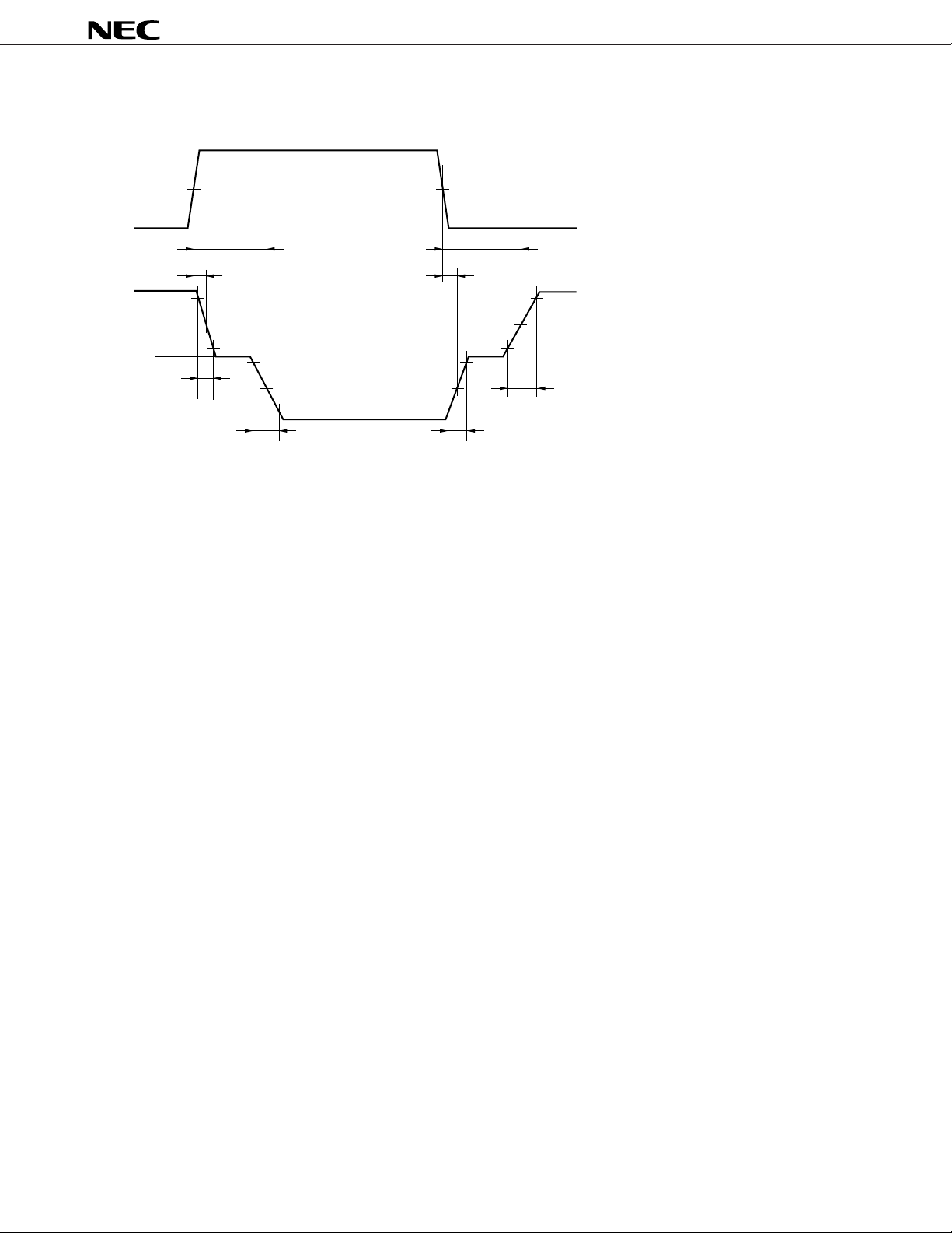
H bridge output circuit turn-ON tONH RM = 20 Ω, Figure 1 0.7 20
time
H bridge output circuit turn-OFF tOFFH 0.2 0.5
time
Rise time tr 0.1 0.4 1.0
Fall time tf 70 200 ns
2
µ
A
µ
A
µ
s

µ
PD16833A
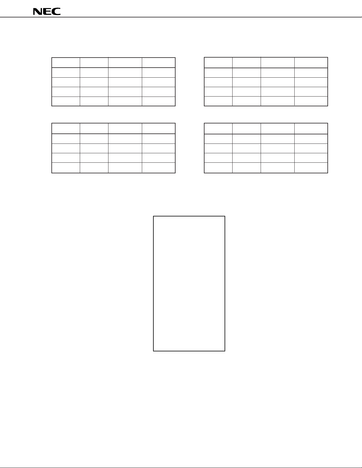
FUNCTION TABLE
Channel 1 Channel 2
EN1 IN1 OUT1A OUT1B EN2 IN2 OUT2A OUT2B
HLH L HLH L
HHL H HHL H
LLZ Z LLZ Z
LHZ Z LHZ Z
Channel 3 Channel 4
EN3 IN3 OUT3A OUT3B EN4 IN4 OUT4A OUT4B
HLH L HLH L
HHL H HHL H
LLZ Z LLZ Z
LHZ Z LHZ Z
H: High level, L: Low level, Z: High impedance IN
PIN CONFIGURATION
NC
1
NC
2
VDD
3
VM1
4
1A
5
PGND
PGND
2A
3A
4A
VM4
IN1
EN1
IN2
EN2
6
7
8
9
10
11
12
13
14
15
30
29
28
27
26
25
24
23
22
21
20
19
18
17
16
NC
NC
DGND
NC
1B
PGND
2B
VM2, 3
3B
PGND
4B
EN4
IN4
EN3
IN3
3

Figure 1. Switching Characteristic Wave
100 %
µ
PD16833A
V
IN
50 % 50 %
0 %
t
t
ON
t
100 %
OFF
90 %
I
DR
0 %
50 %
10 %
–10 %
t
f
–50 % –50 %
–90 % –90 %
t
r
–100 %
ON
t
OFF
100 %
90 %
50 %
10 %
–10 %
t
r
The current flowing in the direction from
OUT_A to OUT_B is assumed to be (+).
f
t
4
 Loading...