NEC UPD16808GS Datasheet

DATA SHEET
MOS INTEGRATED CIRCUIT
µ
PD16808
MONOLITHIC DUAL H BRIDGE DRIVER CIRCUIT
DESCRIPTION
The µPD16808 is a monolithic dual H bridge driver circuit which employing N-channel power MOS FETs for its driver
stage. By using the power MOS FETs for the output stage, saturation voltage and power consumption are substantially
improved as compared with conventional driver circuits that use bipolar transistors.
Because the dual H bridge driver circuits at the output stage are independent of each other, this IC is ideal as the driver
circuit for a 1- to 2-phase excitation bipolar driving stepping motor for the head actuator of an FDD.
FEATURES
• Low ON resistance (sum of ON resistors of top and bottom FETS)
ON1 = 1.0 Ω TYP. (VM = 5.0 V)
R
RON2 = 1.5 Ω TYP. (VM = 12.0 V)
• Low current consumption: IDD = 0.4 mA TYP.
• Four input modes independently controlling dual H bridge drivers (with 1- to 2-phase excitation selected)
• Motor voltage 12 V/5 V compatible
• Compact surface mount package: 20-pin plastic SOP (300 mil)
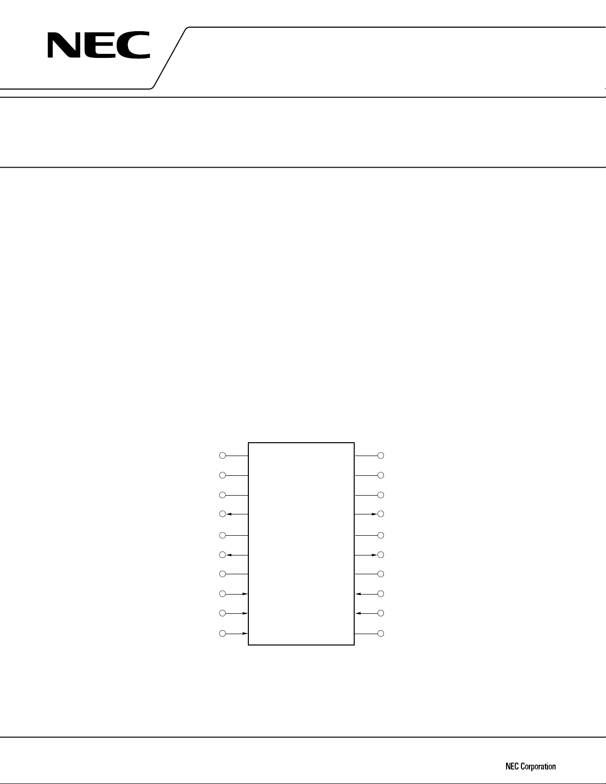
PIN CONFIGURATION (Top View)
C1H
C2L
V
M1
1A
1
PGND
2A
V
DD
IN
1
IN
2
IN
3
1
2
3
4
5
6
7
8
9
10
20
19
18
17
16
15
14
13
12
11
C1L
C2H
V
G
1B
PGND
2B
V
M2
SEL
4
IN
DGND
2
Document No. S12720EJ2V0DS00 (2nd edition)
Date Published September 1997 N
Printed in Japan
©
1997

ORDERING INFORMATION
Part Number Package
µ
PD16808GS 20-pin plastic SOP (300 mil)
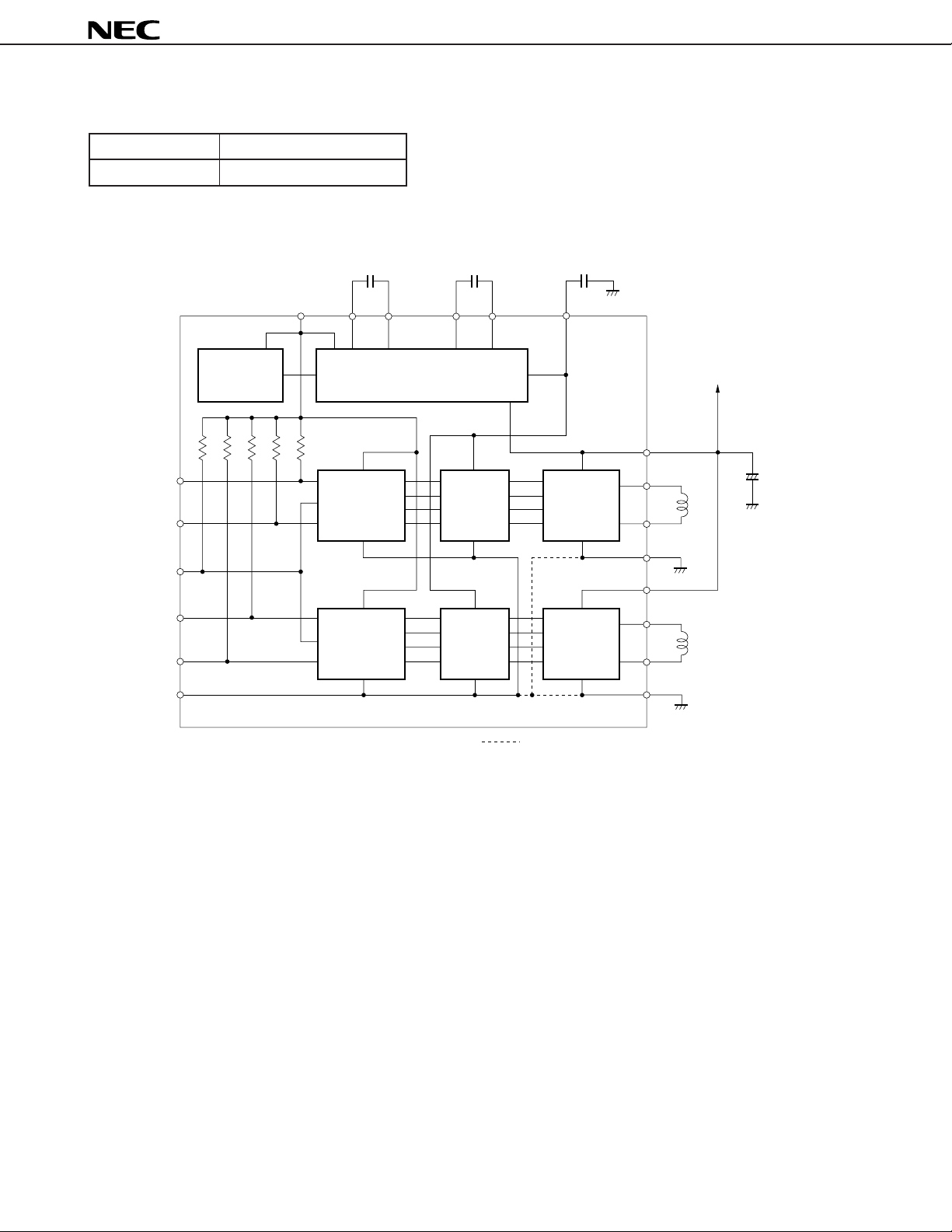
BLOCK DIAGRAM
0.01 F
µ
0.01 F
µ
0.01 F
µ
µ
PD16808
IN
IN
SEL
IN
IN
DGND
C1L C2LC1H C2H
V
DD
OSC
CIRCUIT
1
2
3
4
CHARGE PUMP
CONTROL
CIRCUIT 1
CONTROL
CIRCUIT 2
LEVEL
SHIFT 1
LEVEL
SHIFT 2
V
G
2 × V
“H”
BRIDGE 1
“H”
BRIDGE 2
DD
+ V
M
V
M1
1A
V
M
+
1B
PGND
1
V
M2
2A
2B
2
PGND
Connected in diffusion layer
2

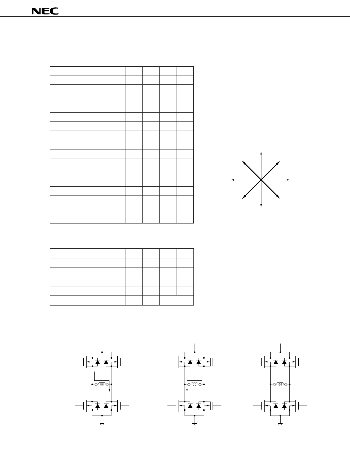
FUNCTION TABLE
• With 1- to 2-phase excitation selected (SEL = High)
µ
PD16808
Excitation Direction
—— LLLLSS
H2R LLLHSR
H2FLLHLSF
—— L L H H S S
H1RLHLLRS
<3> L H L H R R
<2> L H H L R F
H1R LHHHRS
H1F HLLLFS
<4> H L L H F R
<1> HLHLFF
H1FHLHHFS
—— H H L L S S
H2RHHLHSR
H2F HHHLSF
—— HHHHSS
IN1 IN2 IN3 IN4 H1 H2
H2R
<4>
H
1
F
<1>
H
2
F
<2><3>
1
R
H
• With 2-phase excitation selected (SEL = Low)
Excitation Direction
<1> H H × HFF
<2> L H × HRF
<3> L L × HRR
<4> H L × HFR
– ×××L Stop
F: Forward R: Reverse S: Stop ×: Don’t care
IN1 IN3 IN4 IN2 H1 H2
For the excitation waveform timing chart, refer to APPLICATION CIRCUIT EXAMPLE.
FORWARD
M
V
ON
AB
OFF
OFF
ON
OFF
REVERSE
M
V
AB
ON
ON
OFF
STOP
M
V
OFF
AB
OFF
OFF
OFF
3

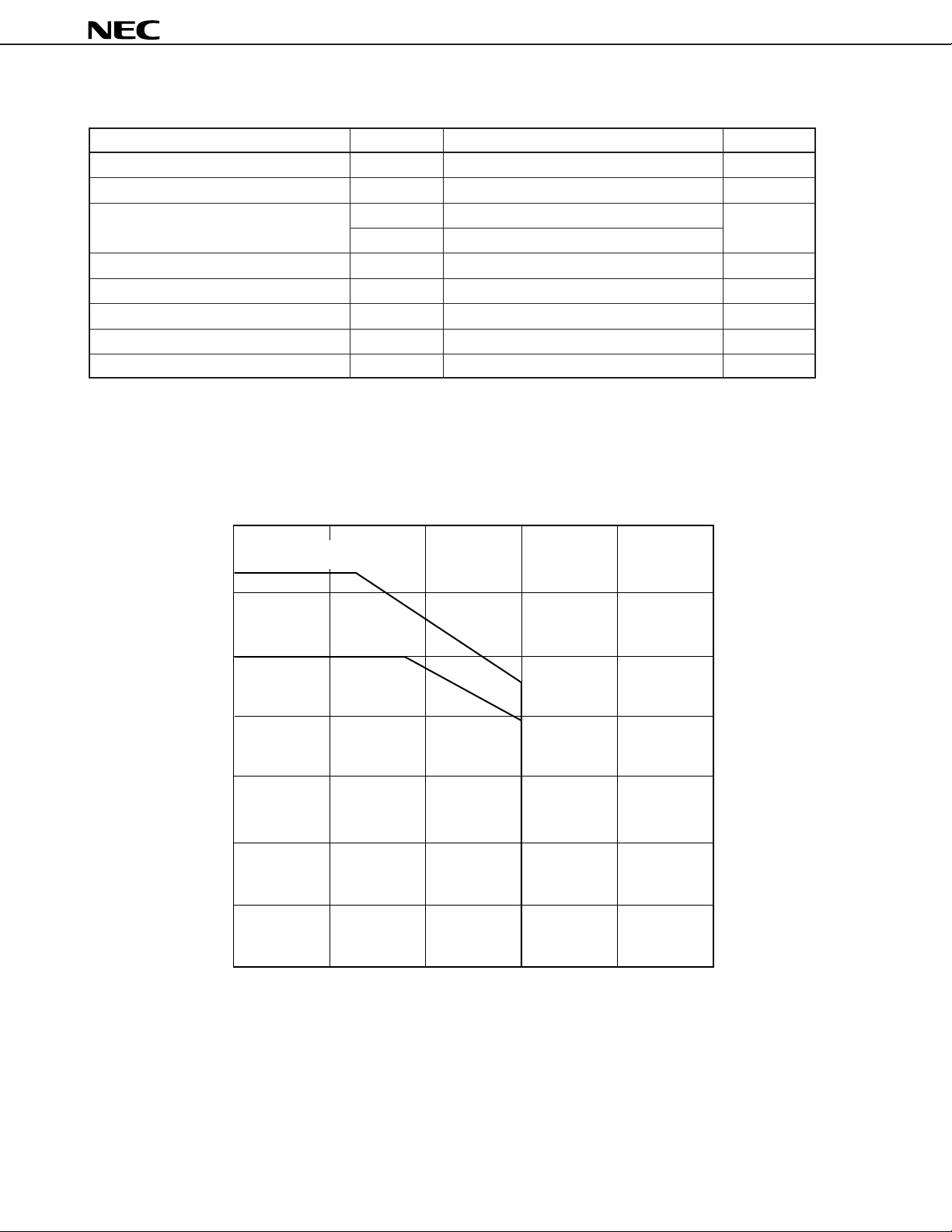
ABSOLUTE MAXIMUM RATINGS (TA = 25 °C)
Parameter Symbol Rating Unit
Supply voltage (motor block) VM –0.5 to +15 V
Supply voltage (control block) VDD –0.5 to +7 V
Power dissipation Pd1 1.0
Pd2 1.25
Instantaneous H bridge driver current ID (pulse) ±1.0
Input voltage VIN –0.5 to VDD + 0.5 V
Operating temperature range TA 0 to 60 °C
Operation junction temperature TjMAX. 150 °C
Storage temperature range Tstg –55 to +125 °C
Note 1
Note 2
Note 2, 3
Notes 1. IC only
2. When mounted on a printed circuit board (100 × 100 × 1 mm, glass epoxy)
3. t ≤ 5 ms, Duty ≤ 40 %
µ
PD16808
W
A
1.4
When mounted
on printed circuid boad
1.2
IC only
1.0
(W)
d
0.8
0.6
Average power dissipation P
0.4
0.2
P
d
– TA Characteristics
0 20 40 60 80 100
Ambient temperature TA (˚C)
4
 Loading...