


DATA SHEET
MOS INTEGRATED CIRCUIT
PD16676
µµµµ
1/16, 1/32 DUTY LCD CONTROLLER/DRIVER
DESCRIPTION
µPD16676 is a controller/driver containing RAMs capable of full-dot LCD displays. One of these IC chips can drive
the full-dot LCD up to 61-by-16 dots.
These ICs are the most suitable for Kanji character or Chinese character pagers, as well as graphic pagers,
displaying 16-by-16 dots per character.
FEATURES
LCD driver with built-in display RAM
•
Dot display RAM: 2560 bits
•
Output: 61 segments & 16 commons
•
8-bit parallel interface
•
Oscillation circuit incorporated
•
•
ORDERING INFORMATION
Part Number Package
PD16676P Chips
µ
PD16676W Wafer
µ
PD16676GF-3BA 100-PIN PLASTIC QFP (14 x 20 mm)
µ
Remark
Purchasing the above products in terms of chips per wafer requires an exchange of other documents as
well, including a memorandum of the product quality. Therefore, those who are interested in this regard
are advised to contact an NEC salesperson for further details.
The information in this document is subject to change without notice. Before using this document, please
confirm that this is the latest version.
Not all devices/types available in every country. Please check with local NEC representative for
availability and additional information.
Document No. S10561EJ5V0DS00 (5th edition)
Date Published June 1999 NS CP(K)
Printed in Japan
The mark
••••
shows major revised points.
©
1996
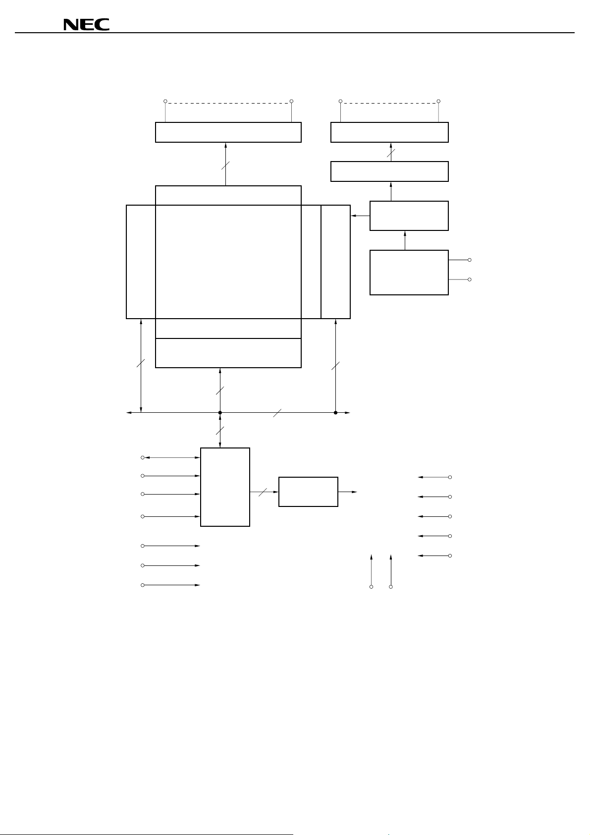
1. BLOCK DIAGRAM
SEG
µµµµ
PD16676
0
SEG
60
COM
0
COM
15
RAM Read/Write
Controller
Column Address Decoder
8
Segment Driver
61
61-bit Latch
Display Data RAM
(2560 bits)
Column Address
Counter & Register
8
Line Preset
Line Address Decoder
8
Common Driver
16
Common Counter
Timing
Generator
Internal
Oscillator
Register & Counter
8
OSC
OSC
1
2
Remark
DB0-DB
7
A0
E(/RD)
R,/W(/WR)
/RESET
M,/S
FR
/xxx indicates active low signals.
8
Parallel
Interface
8
Command
Decoder
VDDV
V
LC1
V
LC2
V
LC3
V
LC4
V
LC5
SS
2
Data Sheet S10561EJ5V0DS00
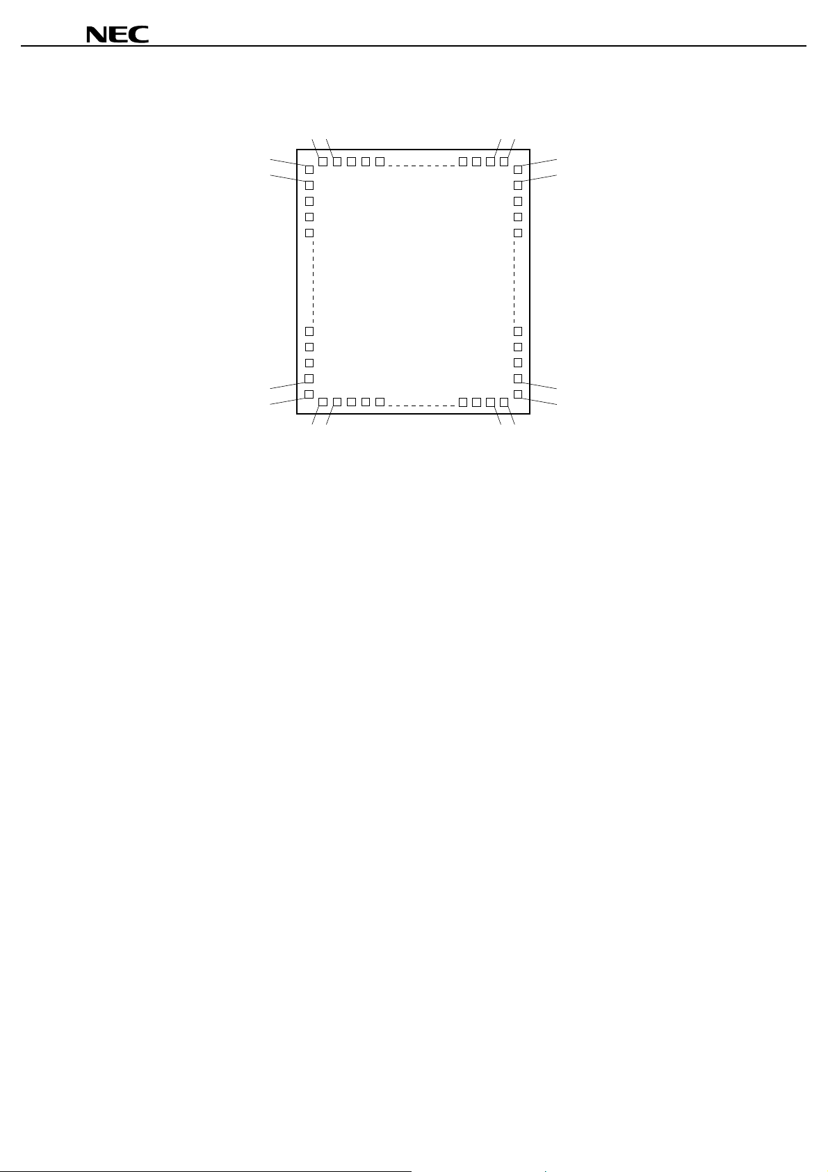
2. PIN CONFIGURATION (Pad Layout)
5049 3231
µµµµ
PD16676
51
52
79
80
30
29
2
1
9981 82
100
Data Sheet S10561EJ5V0DS00
3
3. PIN CONNECTION
Pin No. Pin Symbol I/O Pin No. Pin Symbol I/O
1COM5Output 51 SEG
2COM6Output 52 SEG
3COM7Output 53 SEG
4COM8Output 54 SEG
5COM9Output 55 SEG
6COM10Output 56 SEG
7COM11Output 57 SEG
8COM12Output 58 SEG
9COM13Output 59 SEG
10 COM
11 COM
12 SEG
13 SEG
14 SEG
15 SEG
16 SEG
17 SEG
18 SEG
19 SEG
20 SEG
21 SEG
22 SEG
23 SEG
24 SEG
25 SEG
26 SEG
27 SEG
28 SEG
29 SEG
30 SEG
31 SEG
32 SEG
33 SEG
34 SEG
35 SEG
36 SEG
37 SEG
38 SEG
39 SEG
40 SEG
41 SEG
42 SEG
43 SEG
44 SEG
45 SEG
46 SEG
47 SEG
48 SEG
49 SEG
50 SEG
14
15
60
59
58
57
56
55
54
53
52
51
50
49
48
47
46
45
44
43
42
41
40
39
38
37
36
35
34
33
32
31
30
29
28
27
26
25
24
23
22
Output 60 SEG
Output 61 SEG
Output 62 SEG
Output 63 SEG
Output 64 SEG
Output 65 SEG
Output 66 SEG
Output 67 SEG
Output 68 SEG
Output 69 SEG
Output 70 SEG
Output 71 SEG
Output 72 SEG
Output 73 A0 Input
Output 74 OSC
Output 75 OSC
Output 76 E(/RD) Input
Output 77 R,/W(/WR) Input
Output 78 V
Output 79 DB
Output 80 DB
Output 81 DB
Output 82 DB
Output 83 DB
Output 84 DB
Output 85 DB
Output 86 DB
Output 87 V
Output 88 /RESET Input
Output 89 FR Input/Output
Output 90 V
Output 91 V
Output 92 V
Output 93 M,/S Input
Output 94 V
Output 95 V
Output 96 COM
Output 97 COM
Output 98 COM
Output 99 COM
Output 100 COM
21
20
19
18
17
16
15
14
13
12
11
10
9
8
7
6
5
4
3
2
1
0
1
2
SS
0
1
2
3
4
5
6
7
DD
LC5
LC3
LC2
LC4
LC1
0
1
2
3
4
µµµµ
PD16676
Output
Output
Output
Output
Output
Output
Output
Output
Output
Output
Output
Output
Output
Output
Output
Output
Output
Output
Output
Output
Output
Output
Input
Output
—
Input/Output
Input/Output
Input/Output
Input/Output
Input/Output
Input/Output
Input/Output
Input/Output
—
—
—
—
—
—
Output
Output
Output
Output
Output
4
Data Sheet S10561EJ5V0DS00
4. PIN COORDINATES
µµµµ
PD16676
Chip Size : 4.04 x 5.53 mm
Pad Size Al Area : 120 x 120 µm
Pad Size Open Area : 108 x 108 µm
Pin No. X (µm) Y (µm) Pin No. X (µm) Y (µm) Pin No. X (µm) Y (µm)
1 1771
2 1771
3 1771
4 1771
5 1771
6 1771
7 1771
8 1771
9 1771
10 1771
11 1771
12 1771
13 1771
14 1771
15 1771
16 1771 80 51
17 1771 234 52
18 1771 388 53
19 1771 542 54
20 1771 696 55
21 1771 850 56
22 1771 1004 57
23 1771 1158 58
24 1771 1312 59
25 1771 1466 60
26 1771 1620 61
27 1771 1774 62
28 1771 1928 63
29 1771 2082 64
30 1771 2236 65
31 1418.8 2517.2 66
32 1268.8 2517.2 67
33 1118.8 2517.2 68
34 968.8 2517.2 69
35 818.8 2517.2 70
2230 36 668.8 2517.2 71
−
2076 37 518.8 2517.2 72
−
1922 38 368.8 2517.2 73
−
1768 39 218.8 2517.2 74
−
1614 40 68.8 2517.2 75
−
1460 41
−
1306 42
−
1152 43
−
998 44
−
844 45
−
690 46
−
536 47
−
382 48
−
228 49
−
74 50
−
2
2
2
1771
−
1771
−
1767.8
−
1767.8
−
1767.8
−
81.2 2517.2 76
−
231.2 2517.2 77
−
381.2 2517.2 78
−
531.2 2517.2 79
−
681.2 2517.2 80
−
831.2 2517.2 81
−
981.2 2517.2 82
−
1131.2 2517.2 83
−
1281.2 2517.2 84
−
1431.2 2517.2 85
−
1771 2242.8 86
−
1771 2092.8 87
−
1771 1942.8 88
−
1771 1792.8 89
−
1771 1642.8 90
−
1771 1492.8 91 69.8
−
1771 1342.8 92 219.8
−
1771 1192.8 93 369.8
−
1771 1042.8 94 569.8
−
1771 892.8 95 719.8
−
1771 742.8 96 952.4
−
1771 592.8 97 1102.4
−
1771 442.8 98 1252.4
−
1771 292.8 99 1402.4
−
1771 142.8 100 1552.4
−
1771
−
1771
−
1771
−
1771
−
1771
−
−
157.2
−
307.2
−
457.2
−
607.2
−
7.2
1767.8
−
1767.8
−
1767.8
−
1767.8
−
1767.8
−
1745
−
1595
−
1395
−
1245
−
1045
−
895
−
682.6
−
532.2
−
382.2
−
106.6
−
757.2
−
907.2
−
1149.4
−
1299.4
−
1489.4
−
1639.4
−
1839.4
−
1989.4
−
2139.4
−
2289.4
−
2513.4
−
2513.4
−
2513.4
−
2513.4
−
2513.4
−
2513.4
−
2513.4
−
2513.4
−
2513.4
−
2513.4
−
2513.4
−
2513.4
−
2513.4
−
2513.4
−
2513.4
−
2513.4
−
2513.4
−
2513.4
−
2513.4
−
2513.4
−
Data Sheet S10561EJ5V0DS00
5
5. PIN DESCRIPTIONS
5.1 Power System
Pin Symbol Pin Name Pin No. I/O Function Description
µµµµ
PD16676
DD
V
SS
V
LC1
V
to V
Power supply pin
Ground 78
LC5
Reference power supply for
drivers
87 —
90,91,92,
94,95
5.2 Logic system
Pin Symbol Pin Name Pin No. I/O
M,/S Master/Slave selection 93
FR LCD to AC signal 89
DB0 to DB7Data Bus 79 to 86
A0 Data/Instruction Switching 73
/RESET Reset and 68/80-series
switching
E(/RD) Enable and read enabl e 76
R,/W(/WR) Read/Write and Write
enable
1
OSC
OSC
2
Oscillation pin 74
Oscillation pin 75
88
77
—
—
Input
Input/
Output
Input/
Output
Input
Input
Input
Input
Input
Output
Power supply
Ground
Reference power supply for LCD driving
Function Description
Switches between the master c hi p and the slave
chip.
Exchanges synchronizing signals (LCD-to-AC
signals) in connecting c ascades.
This pin is for output if the chip is the master, and for
input if the chip is t he slave.
Data inputs/outputs
This pin is used for switchi ng between the display
data and the instruction.
High level : Display data
Low level : Instruction
This pin performs reset at the edge of the low-level
pulse. At that level, i t performs switching 68/80
series modes.
High level : 68 series MPU int erface
Low level : 80 series MPU interfac e
68 series mode : Enable s i gnal
80 series mode : Read enable si gnal
68 series mode : Read/Write signal
80 series mode : Write enable signal
Oscillation (connected with a register bet ween
2
)
OSC
Oscillation (connected with a register bet ween
1
)
OSC
5.3 Driver System
Pin Symbol Pin Name Pin No. I/O Description
SEG0 to
SEG
COM0 to
COM
6
Segment 72 to 12
60
Common 96 to 100,
15
1 to 11
Data Sheet S10561EJ5V0DS00
Output
Output
Segment output pins
Common output pins
If the chip is a slave, these pins correspond to
16
to COM31.
COM

6. COMMANDS
µµµµ
PD16676
(0 to 3)
0
performed independent of the
display RAM’s data or internal
state.
1: ON, 0: OFF (Power save at
static drive ON)
Determines the RAM lin e
displayed on the uppermost li ne
(COM
Sets display RAM pages i n the
page address register.
Sets display RAM’s column
address in the column addres s
register.
BUSY
1: During internal operation
0: READY status
ADC
1: Clockwise output(Normal
rotation)
0: Counterclockwise output
(Reverse)
ON/OFF
1: Display OFF, 0: Display ON
RESET
1: Being reset, 0: Norm al
data bus data
and writes it
onto the
display RAM.
in the display
RAM onto the
data bus.
reverse the correspondence
relationship between display
RAM’s column addresses and
segment driver outputs.
0: Clockwise output (Normal
rotation)
1: Counterclockwise output
(Reverse)
display operation and the stati c
all-lamp-driven display.
1: Static drive (Power save)
0: Normal display operati on
liquid-crystal cel l dri vi ng duties.
1: 1/32 duty
0: 1/16 duty
counter only when writing the
display data; but not when
reading it.
register to the first l i ne.
Sets the column address
counter and the page address
register to 0.
Function
Note
0
) of the display.
Accesses the
display RAM of
a pre-specified
address. After
access, the
column
address is
incremented.
Note
Command /RD /WR A0 DB7DB6DB5DB4DB3DB2DB1DB
1Display ON/OFF 10010101110/1ON/OFF of the whole display is
2Display start line 100110 Display start address
3 Page address set 100101110 Pages
4 Column(s egment)
address set
5 Status read 0 1 0 B
6 Display dat a write 1 0 1 Write Data Displays the
7 Display data read 0 1 1 Read data Reads the data
8ADC select 10010100000/1This command is used to
9 Static drive
ON/OFF
10Duty select 10010101000/1Selects between two different
11 Read modify write 10011100000Increments the column address
12END 10011101110Cancels read modify write mode
13Reset 10011100010Sets the display start line
Note
If the static drive is turned ON in the display OFF state, the machine is placed in the power save state.
1000 Column addresses
A
O
U
D
S
C
Y
10010100100/1Selects between the normal
R
N
E
/
S
O
E
F
T
F
(0 to 31)
(0 to 79)
0000Reads status
Data Sheet S10561EJ5V0DS00
7

7. DISPLAY RAM MAP
DB
0
DB
7
µµµµ
PD16676
Column Address
079
0
Page 0
(640 bits)
7
8
Page 1
(640 bits)
15
16
23
24
31
Line Address
Page 2
(640 bits)
Page 3
(640 bits)
8
Data Sheet S10561EJ5V0DS00

•
8. Line Address Circuit
As is shown in Figure 8-1, the line address circuit specifies the line address that corresponds to a COM output for
displaying the contents of display data RAM. The display start line address set command specifies line address of to
0
the COM
output.
The screen can be scrolled by dynamically changing the line address via the display start line address set
command.
Figure 8-1. Specification of Display Start Line Address in Display Data RAM
µµµµ
PD16676
Page
Address
DB
DB1
0
0
1
1
3BH
14H
3CH
13H
60
Line
Address
00H
01H
02H
03H
04H
05H
06H
07H
08H
09H
0AH
0BH
0CH
0DH
0EH
0FH
10H
11H
12H
13H
14H
15H
16H
17H
18H
19H
1AH
1BH
1CH
1DH
1EH
1FH
0
0
DB
0
ADC
1
LCD
DB
Out
Column
Address
Data
0
DB0
DB1
DB2
DB3
0
DB4
DB5
DB6
DB7
DB0
DB1
DB2
DB3
1
DB4
DB5
DB6
DB7
DB0
DB1
DB2
DB3
0
DB4
DB5
DB6
DB7
DB0
DB1
DB2
DB3
1
DB4
DB5
DB6
DB7
00H
01H
02H
03H
04H
05H
4FH
4EH
4DH
4CH
4BH
4AH
SEG0SEG1SEG2SEG3SEG4SEG5SEG6SEG
06H
49H
07H
48H
7
Page0
Page1
Page2
Page3
35H
36H
37H
38H
39H
3AH
1AH
19H
18H
17H
16H
15H
SEG53SEG54SEG55SEG56SEG57SEG58SEG59SEG
COM
Output
COM
COM1
COM2
COM3
COM4
COM5
COM6
COM7
COM8
COM9
COM10
COM11
COM12
COM13
COM14
COM15
COM16
COM17
COM18
COM19
COM20
COM21
COM22
COM23
COM24
COM25
COM26
COM27
COM28
COM29
COM30
COM31
0
Remark
16
COM
to COM31 are valid in only 1/32 duty.
Data Sheet S10561EJ5V0DS00
9

•
9. ELECTRICAL SPECIFICATIONS
µµµµ
PD16676
Absolute Maximum Ratings (TA = 25
C, VSS = 0 V)
°°°°
Parameter Symbol Rating Unit
Supply voltage V
Driver reference supply input volt age V
Driver reference supply input volt age V
Logic system input vol t age V
Logic system output vol tage V
Logic system input / output voltage V
Driver system output voltage V
Operating ambient tem perature T
Storage temperature T
DD
LC1
LC5
IN1
OUT1
I/O1
OUT2
A
stg
to V
LC4
–0.3 to +6.5 V
VDD–13 to VDD+0.3 V
VDD–13 to +0.3 V
DD
0.3 to V
−
0.3 to V
−
0.3 to V
−
LC5
V
–0.3 to VDD + 0.3 V
−
+ 0.3 V
DD
+ 0.3 V
DD
+ 0.3 V
40 to +85
−
65 to +150
Cautions 1. If the absolute maximum rating of even one of the above parameters is exceeded even
momentarily, the quality of the product may be degraded. Absolute maximum ratings, therefore,
specify the values exceeding which the product may be physically damaged. Be sure to use the
product within the range of the absolute maximum ratings.
DD
LC1
LC2
LC3
LC4
2. Ensure that the phase relationship is V
Recommended Operating Range (V
Parameter Symbol MIN. TYP. MAX. Unit
SS
= 0 V)
V
V
V
≥≥≥≥
≥≥≥≥
≥≥≥≥
V
≥≥≥≥
LC5
V
.
≥≥≥≥
C
°
C
°
Supply voltage V
Reference supply voltage V
Reference supply voltage V
Logic system input vol t age V
DD
LC1
LC5
IN1
to V
LC4
2.7 5.5 V
VDD–12 V
DD
V
VDD–12 0 V
0V
DD
V
10
Data Sheet S10561EJ5V0DS00

µµµµ
PD16676
Electrical Characteristics (Unless otherwise specified, T
Parameter Symbol Condition MIN.
High-level input voltage V
High-level input voltage V
Low-level input voltage V
Low-level input voltage V
High-level input current I
Low-level input current I
High-level output voltage V
High-level output voltage V
High-level output voltage V
Low-level output voltage V
Low-level output voltage V
Low-level output voltage V
High-level output voltage V
High-level output voltage V
High-level output voltage V
Low-level output voltage V
Low-level output voltage V
Low-level output voltage V
High-level leak current I
Low-level leak current I
Driver output ON resistor R
Driver output ON resistor R
Static current consumption I
Dynamic current consumption I
Dynamic current consumption I
Input capacitance C
Oscillator frequency f
Oscillator frequency f
Reset time t
IH1
IH2
IL1
IL2
IH
IL
OH1
OH2
OH3
OL1
OL2
OL3
OH1
OH2
OH3
OL1
OL2
OL3
LOH
LOL
ON
ON
DD0
DD1
DD3
IN
OSC
OSC
R
A0, DB0 to DB7, E, R,/W 0.8 V
FR, M,/S, /RESET 0.8 V
A0, DB0 to DB7, E, R,/W 0.2 V
FR, M,/S, /RESET 0.2 V
A0, E, R,/W, /RESET
A0, E, R,/W, /RESET –1
OUT
I
= –3 mA, DB0 to DB7,
DD
= 4.5 to 5.5 V
V
OUT
I
= –2 mA, FR, VDD = 4.5 to 5.5 V 0.8 V
OUT
I
= –120 µA, OSC2,
DD
= 4.5 to 5.5 V
V
OUT
I
= 3 mA, DB0 to DB7,
DD
= 4.5 to 5.5 V
V
OUT
I
= 2 mA, FR, VDD = 4.5 to 5.5 V 0.2 V
OUT
I
= 120 µA, OSC2,
DD
= 4.5 to 5.5 V
V
OUT
I
= –1.5 mA, DB0 to DB7,
DD
= 2.7 to 4.5 V
V
OUT
I
= –1 mA, FR, VDD = 2.7 to 4.5 V 0.8 V
OUT
I
= –80 µA, OSC2,
DD
= 2.7 to 4.5 V
V
OUT
I
= 1.5 mA, DB0 to DB7,
DD
= 2.7 to 4.5 V
V
OUT
I
= 1 mA, FR, VDD = 2.7 to 4.5 V 0.2 V
OUT
I
= 80 µA, OSC2,
DD
= 2.7 to 4.5 V
V
DB0 to DB7, V
DB0 to DB7, V
TA = 25 °C, VDD = 5 V, V
TA = 25 °C, VDD = 3.5 V, V
External clock: 18 kHz 15.0
Self-oscillation: R = 1.3 M
During access: t
TA = 25 °C, f = 1 MHz 8.0 pF
In self-oscillation, VDD = 5.0 V,
R = 1.3 M
Ω ±
In self-oscillation, VDD = 3.0 V,
R = 1.3 M
Ω ±
/RESET↓→Internal reset release 1.0 1000
A =
0 to +85
−4
−4
−4−4
C, V
°°°°
DD
= 2.7 to 5.5 V)
TYP.
DD
DD
DD
0.8 V
DD
DD
0.8 V
DD
0.8 V
DD
DD
0.8 V
IN/OUT
IN/OUT
= V
= V
DD
SS
LC5
SS
= V
LC5
SS
= V
Ω
CYC
= 200 kHz 500
15 18 21 kHz
2%
11 16 21 kHz
2%
Note
MAX. Unit
DD
DD
1
DD
0.2 V
DD
DD
0.2 V
DD
0.2 V
DD
DD
0.2 V
3
–3
7.5 k
50 k
1.0
30.0
V
V
V
V
A
µ
A
µ
V
V
V
V
V
V
V
V
V
V
V
V
A
µ
A
µ
Ω
Ω
A
µ
A
µ
A
µ
A
µ
s
µ
Remark
The TYP. value is a reference value when T
Data Sheet S10561EJ5V0DS00
A
= 25 °C.
11

AC Characteristics 1 (Unless otherwise specified, TA =
80 Series MPU Read/Write Timing
Parameter Symbol Condition MIN. TYP. M AX. Unit
4
0 to +85
−−−−
C, V
°°°°
DD
= 4.5 to 5.5 V)
µµµµ
PD16676
Address hold time t
Address setup time t
System cycle time t
Control pulse width t
Data setup time t
Data hold time t
/RD access time t
Output disable time t
68 Series MPU Read/Write Timing
Parameter Symbol Condition MIN. TYP. MAX. Unit
System cycle time t
Address setup time t
Address hold time t
Data setup time t
Data hold time t
Output disable time t
Access time t
Enable pulse width READ t
WRITE 80 ns
AH8
AW8
CYC8
CC
DS8
DH8
ACC8
OH8
CYC6
AW6
AH6
DS6
DH6
OH6
ACC6
EW
A0 10 ns
20 ns
/WR, /RD 1000 ns
200 ns
DB0 to DB
7
80 ns
10 ns
DB0 to DB7 , CL = 100 pF 90 ns
10 60 ns
A0, R,/W 1000 ns
20 ns
10 ns
DB0 to DB
7
80 ns
10 ns
DB0 to DB7, CL = 100 pF 10 60 ns
90 ns
E 100 ns
12
Data Sheet S10561EJ5V0DS00

AC Characteristics 2 (Unless otherwise specified, TA =
80 Series MPU Read/Write Timing
Parameter Symbol Condition MIN. TYP. M AX. Unit
4
0 to +85
−−−−
C, V
°°°°
DD
= 2.7 to 4.5 V)
µµµµ
PD16676
Address hold time t
Address setup time t
System cycle time t
Control pulse width t
Data setup time t
Data hold time t
/RD access time t
Output disable time t
68 Series MPU Read/Write Timing
Parameter Symbol Condition MIN. TYP. MAX. Unit
System cycle time t
Address setup time t
Address hold time t
Data setup time t
Data hold time t
Output disable time t
Access time t
Enable pulse width READ t
WRITE 160 ns
AH8
AW8
CYC8
CC
DS8
DH8
ACC8
OH8
CYC6
AW6
AH6
DS6
DH6
OH6
ACC6
EW
A0 20 ns
40 ns
/WR, /RD 2000 ns
400 ns
DB0 to DB
7
160 ns
20 ns
DB0 to DB7 , CL = 100 pF 180 ns
20 120 ns
A0, R,/W 2000 ns
40 ns
20 ns
DB0 to DB
7
160 ns
20 ns
DB0 to DB7, CL = 100 pF 20 120 ns
180 ns
E 200 ns
Data Sheet S10561EJ5V0DS00
13

Test Point of Switching Characteristics
V
IH
Input
V
IL
V
OH
Output
V
OL
Waveforms of Switching Characteristics
80 Series MPU Read/Write Timing
A0
µµµµ
PD16676
V
IH
V
IL
V
OH
V
OL
t
AH8
t
AW8
/WR,/RD
DB0 - DB
(WRITE)
DB
0
- DB
(READ)
7
7
68 Series MPU Read/Write Timing
E
R,/W
t
ACC8
t
AW6
t
t
CYC8
CC
t
DS8
t
CYC6
t
DH8
t
OH8
t
EW
t
AH6
A0
DB0 - DB
(READ)
DB0 - DB
(READ)
14
t
t
DS6
7
t
ACC6
7
Data Sheet S10561EJ5V0DS00
DH6
t
OH6

Reset
/RESET
µµµµ
PD16676
t
R
Internal Status
OSC
OSC
1/f
OSC
Reset status
Data Sheet S10561EJ5V0DS00
15

•
10. Application Circuit Example
16 COM
V
DD
M,/S
µ
PD16676
Master Chip
61 SEG
FR
LCD
OSC
OSC
µµµµ
PD16676
1
2
A0,
/RESET,
E,/RD,
R,/W, /WR
DB
0
- DB
61 SEG
16 COM
4
7
8
M,/S
GND
PD16676
µ
Slave Chip
FR
OSC
1
16
Data Sheet S10561EJ5V0DS00

•
11. PACKAGE DRAWING
100 PIN PLASTIC QFP (14x20)
µµµµ
PD16676
A
B
80
81
100
1
F
G
H
M
I
P
S
N
NOTE
Each lead centerline is located within 0.15 mm of
its true position (T.P.) at maximum material condition.
51
50
detail of lead end
S
CD
31
Q
30
R
J
K
M
L
S
ITEM MILLIMETERS
A 23.2±0.2
B 20.0±0.2
C 14.0±0.2
D
17.2±0.2
F
0.8
G
0.6
H 0.32±0.08
I
0.15
J
0.65 (T.P.)
K 1.6±0.2
L 0.8±0.2
M 0.17
N 0.10
P 2.7
Q
R5°±5°
S 2.825±0.175
+0.08
−0.07
0.125±0.075
S100GF-65-3BA-4
Data Sheet S10561EJ5V0DS00
17

•
12. RECOMMENDED SOLDERING CONDITIONS
Please consult with our sales offices for soldering conditions of the µPD16676.
Type of Surface Mount Device
µPD16676GF-3BA : 100-PIN PLASTIC QFP (14 x 20 mm)
µµµµ
PD16676
18
Data Sheet S10561EJ5V0DS00

NOTES FOR CMOS DEVICES
1 PRECAUTION AGAINST ESD FOR SEMICONDUCTORS
Note:
Strong electric field, when exposed to a MOS device, can cause destruction of the gate oxide and
ultimately degrade the device operation. Steps must be taken to stop generation of static electricity
as much as possible, and quickly dissipate it once, when it has occurred. Environmental control
must be adequate. When it is dry, humidifier should be used. It is recommended to avoid using
insulators that easily build static electricity. Semiconductor devices must be stored and transported
in an anti-static container, static shielding bag or conductive material. All test and measurement
tools including work bench and floor should be grounded. The operator should be grounded using
wrist strap. Semiconductor devices must not be touched with bare hands. Similar precautions need
to be taken for PW boards with semiconductor devices on it.
2 HANDLING OF UNUSED INPUT PINS FOR CMOS
Note:
No connection for CMOS device inputs can be cause of malfunction. If no connection is provided
to the input pins, it is possible that an internal input level may be generated due to noise, etc., hence
causing malfunction. CMOS devices behave differently than Bipolar or NMOS devices. Input levels
of CMOS devices must be fixed high or low by using a pull-up or pull-down circuitry. Each unused
DD
pin should be connected to V
being an output pin. All handling related to the unused pins must be judged device by device and
related specifications governing the devices.
or GND with a resistor, if it is considered to have a possibility of
µµµµ
PD16676
3 STATUS BEFORE INITIALIZATION OF MOS DEVICES
Note:
Power-on does not necessarily define initial status of MOS device. Production process of MOS
does not define the initial operation status of the device. Immediately after the power source is
turned ON, the devices with reset function have not yet been initialized. Hence, power-on does
not guarantee out-pin levels, I/O settings or contents of registers. Device is not initialized until the
reset signal is received. Reset operation must be executed immediately after power-on for devices
having reset function.
Data Sheet S10561EJ5V0DS00
19

µµµµ
PD16676
• The information in this document is subject to change without notice. Before using this document, please
confirm that this is the latest version.
• No part of this document may be copied or reproduced in any form or by any means without the prior written
consent of NEC Corporation. NEC Corporation assumes no responsibility for any errors which may appear in
this document.
• NEC Corporation does not assume any liability for infringement of patents, copyrights or other intellectual property
rights of third parties by or arising from use of a device described herein or any other liability arising from use
of such device. No license, either express, implied or otherwise, is granted under any patents, copyrights or other
intellectual property rights of NEC Corporation or others.
• Descriptions of circuits, software, and other related information in this document are provided for illustrative
purposes in semiconductor product operation and application examples. The incorporation of these circuits,
software, and information in the design of the customer's equipment shall be done under the full responsibility
of the customer. NEC Corporation assumes no responsibility for any losses incurred by the customer or third
parties arising from the use of these circuits, software, and information.
• While NEC Corporation has been making continuous effort to enhance the reliability of its semiconductor devices,
the possibility of defects cannot be eliminated entirely. To minimize risks of damage or injury to persons or
property arising from a defect in an NEC semiconductor device, customers must incorporate sufficient safety
measures in its design, such as redundancy, fire-containment, and anti-failure features.
• NEC devices are classified into the following three quality grades:
"Standard", "Special", and "Specific". The Specific quality grade applies only to devices developed based on a
customer designated "quality assurance program" for a specific application. The recommended applications of
a device depend on its quality grade, as indicated below. Customers must check the quality grade of each device
before using it in a particular application.
Standard: Computers, office equipment, communications equipment, test and measurement equipment,
audio and visual equipment, home electronic appliances, machine tools, personal electronic
equipment and industrial robots
Special: Transportation equipment (automobiles, trains, ships, etc.), traffic control systems, anti-disaster
systems, anti-crime systems, safety equipment and medical equipment (not specifically designed
for life support)
Specific: Aircraft, aerospace equipment, submersible repeaters, nuclear reactor control systems, life
support systems or medical equipment for life support, etc.
The quality grade of NEC devices is "Standard" unless otherwise specified in NEC's Data Sheets or Data Books.
If customers intend to use NEC devices for applications other than those specified for Standard quality grade,
they should contact an NEC sales representative in advance.
M7 98. 8
 Loading...