NEC UPD16510GR-8JG Datasheet

DATA SHEET
MOS INTEGRATED CIRCUIT
µ
PD16510
VERTICAL DRIVER FOR CCD SENSOR
The µPD16510 is a vertical driver dedicated for CCD area image sensors that incorporates a level conversion
circuit and a three-level output function. It contains a CCD vertical register driver (4 channels) and a VOD shutter
driver (1 channel).
µ
PD16510, which uses the CMOS process, provides optimum transmission delay and output ON resistance
The
characteristics for the vertical drive of CCD sensors. It can be used for low-voltage logic (logic power-supply voltage:
2.0 to 5.5 V).
FEATURES
•CCD vertical register driver: 4 channels, VOD shutter driver: 1 channel
•Small package : 20-pin plastic shrink SOP (225 mil)
•High breakdown voltage : 33 V MAX.
•Low output ON resistance : 30 Ω TYP.
•Low voltage operation (logic power-supply voltage: 2.0 to 5.5 V)
•Latch-up free
µ
•Pin-compatible with
PD16506 (CCD driver)
APPLICATIONS
•Camcorders
ORDERING INFORMATION
Part Number Package
µ
PD16510GR-8JG 20-pin plastic shrink SOP (225 mil)
The information in this document is subject to change without notice.
Document No. S12191EJ2V0DS00 (2nd edition)
(Previous No. IC-3448)
Date Published May 1997 N
Printed in Japan
The mark shows major revised points.
1994

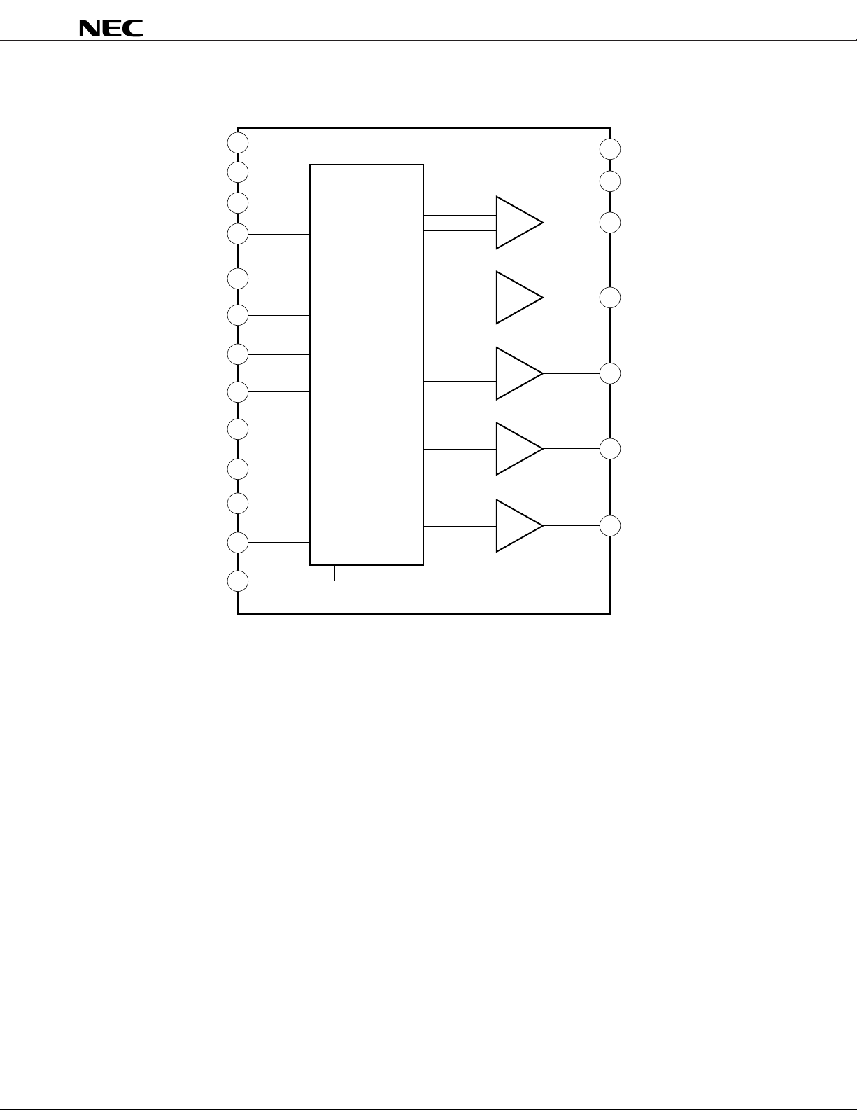
BLOCK DIAGRAM
SUBI
V
PG
PG
V
V
DD1
TI
BI
TI
BI
µ
PD16510
20
sb
16
V
DD1
V
Three
level
Two
level
Three
level
Two
level
DD2a
V
SS
DD2b
V
V
SS
DD2a
V
V
SS
DD2b
V
V
SS
SS
2
1
7
1
8
1
9
V
14
13
2
12
2
(2.0 to 5.5 V)
2
Input interface
DD1
10
19
17
18
4
V
DD2a
V
DD2b
5
TO
1
3
BO
1
TO
2
BO
2
NC
V
GND
sb
Two
level
V
1
SUBO
V
SS
11
CC
6
15
2

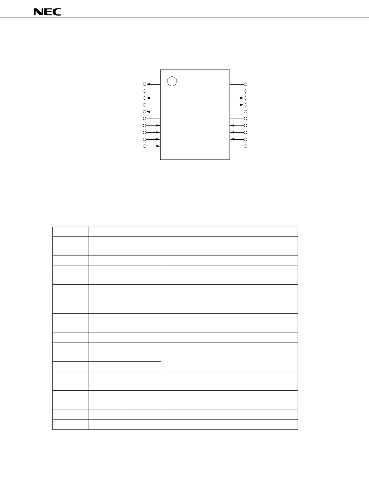
PIN CONFIGURATION
20-pin plastic shrink SOP (225 mil)
µ
PD16510
SUBO
V
BO
V
DD2a
TO
V
TI
PG
BI
SUBI
SS
1
1
CC
1
1
1
10
1
2
3
4
5
6
7
8
9
20
19
18
17
16
15
14
13
12
11
V
V
BO
TO
V
GND
TI
PG
BI
NC
Remark The µPD16510 is pin-compatible with the µPD16506 (CCD driver).
However, the VOD shutter drive pulse input polarity switching pin (SSP) of the
to the GND pin in the µPD16510 (pin 15).
PIN FUNCTIONS
No. Symbol I/O Pin Function
1 SUBO O VOD shutter drive pulse output
2VSS –VL power supply
3BO1 O Two-level pulse output
4VDD2a –VMa (Three-level driver) power supply
5TO1 O Three-level pulse output
6VCC – Logic power supply
7TI1 I Three-level driver input (See Functions table on p. 4)
8PG1 I
9BI1 I Two-level driver input (See Functions table on p. 4)
10 SUBI I VOD shutter drive pulse input
11 NC – Non connect
12 BI2 I Two-level driver input (See Functions table on p. 4)
13 PG2 I Three-level driver input (See Functions table on p. 4)
14 TI2 I
15 GND – Ground
16 VDD1 –VH power supply
17 TO2 O Three-level pulse output
18 BO2 O Two-level pulse output
19 VDD2b –VMb (Two-level driver) power supply
20 Vsb –VHH (for SUB drive) power supply
sb
DD2b
DD1
2
2
2
2
2
µ
PD16506 corresponds
3

FUNCTIONS
VL = VSS, VMa = VDD2a, VMb = VDD2b, VH = VDD1, VHH = Vsb
Pin TO
1
Pin TO2
µ
PD16510
Input
TI1 PG1
LL VH
LH VMa
HL VL
HH
Output (TO1)
Pin BO1
Input
BI1
LVMb
HVL
Output (BO1)
Pin BO2
Input
BI2
LVMb
HVL
Output (BO2)
Input
TI2 PG2
LL VH
LH VMa
HL VL
HH
Output (TO2)
Pin SUBO
Input
SUBI
LVHH
HVL
Output (SUBO)
Usage Caution
Because the µPD16510 contains a PN junction (diode) between VDD2 → VDD1, if the voltage is VDD2 > VDD1, an
abnormal current will result.
Therefore, apply power in the sequence V
DD1 → VDD2, or apply power simultaneously to VDD1 and VDD2.
4

µ
PD16510
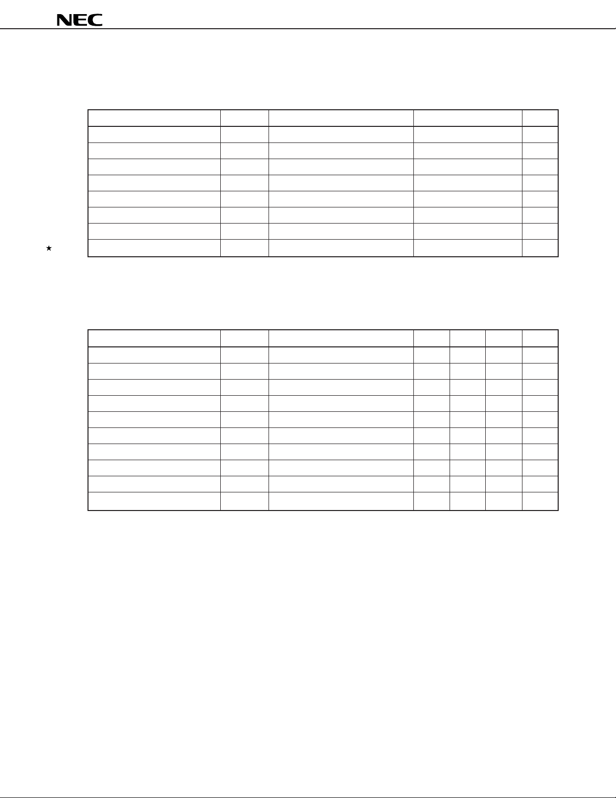
ELECTRICAL SPECIFICATIONS
ABSOLUTE MAXIMUM RATINGS (Unless otherwise specified, TA = 25 ˚C, GND = 0 V)
Parameter Symbol Conditions Rating Unit
Power supply voltage VCC VSS–0.3 to VSS+20.0 V
Power supply voltage VDD1 VSS–0.3 to VSS+33.0 V
Power supply voltage VDD2 VSS–0.3 to VSS+33.0 V
Power supply voltage Vsb VSS–0.3 to VSS+33.0 V
Input voltage VI VSS–0.3 to VCC+0.3 V
Operating ambient temperature TA –25 to +85 °C
Storage temperature Tstg –40 to +125 °C
Power dissipation Pd TA = 85 °C 260 mW
Caution Exposure to Absolute Maximum Rating for extended periods may affect device reliability;
exceeding the ratings could cause permanent damage. The parameters apply independently.
RECOMMENDED OPERATING CONDITIONS (T
Parameter Symbol Conditions MIN. TYP. MAX. Unit
Power supply voltage VCC 2.0 5.5 V
Power supply voltage VDD1 Note 10.5 15.0 21.0 V
Power supply voltage VDD1–VSS Note 20.5 31.0 V
Power supply voltage VDD2a –1.0 +4.0 V
Power supply voltage VDD2b –1.0 +4.0 V
Power supply voltage VSS Note –10.0 –6.0 V
Power supply voltage Vsb–VSS 31.0 V
Input voltage, high VIH –0.8 VCC VCC V
Input voltage, low VIL 0 0.3 VCC V
Operating ambient temperature TA –20 +70 °C
A = 25 ˚C, GND = 0 V)
Note Set the values of VDD1 and VSS to conform to VDD1–VSS specification value.
5
 Loading...