NEC UPC7073GT Datasheet

DATA SHEET
BIPOLAR ANALOG INTEGRATED CIRCUIT
µ
PC7073
µ
PC7073 ANALOG SUBSCRIBER LINE LSI (BS-SLIC)
The µPC7073 is a BS-SLIC that can be used in analog subscriber circuits such as private branch exchangers
(PBXs) and switching equipment for central offices. It features two of the functions required for analog subscriber
circuits: subscriber line feed control and subscriber line supervision.
µ
Use of the
required in analog subscriber circuits.
FEATURES
• Single-chip, monolithic LSI (bipolar)
• Constant-resistance feed or semi constant-current feed
• 200-Ω feed, 400-Ω feed, or Tip-to-Ring pin feedout status (HIGH and WET)
• On-chip metering signal superposing circuit
• On-hook sending and receiving
• Loop detection
• Ground detection and ground-fault/power contact protection
• Three on-chip relay drivers (flyback prevention diode must be externally provided)
• Two power supply voltages (–48 V and +5 V)
• Low power consumption: 110 mW (TYP., when on hook)
PC7073 in combination with a digital CODEC (µPD9903) can reduce the number of components
Note
Note
Note
µ
Note Requires
ORDERING INFORMATION
Part Number Package
µ
PC7073GT 48-pin plastic shrink SOP (375 mil)
PD9903.
The information in this document is subject to change without notice.
Document No. S10896EJ2V0DS00 (2nd edition)
(Previous No. ID-3576)
Date Published June 1996 P
Printed in Japan
©
1996

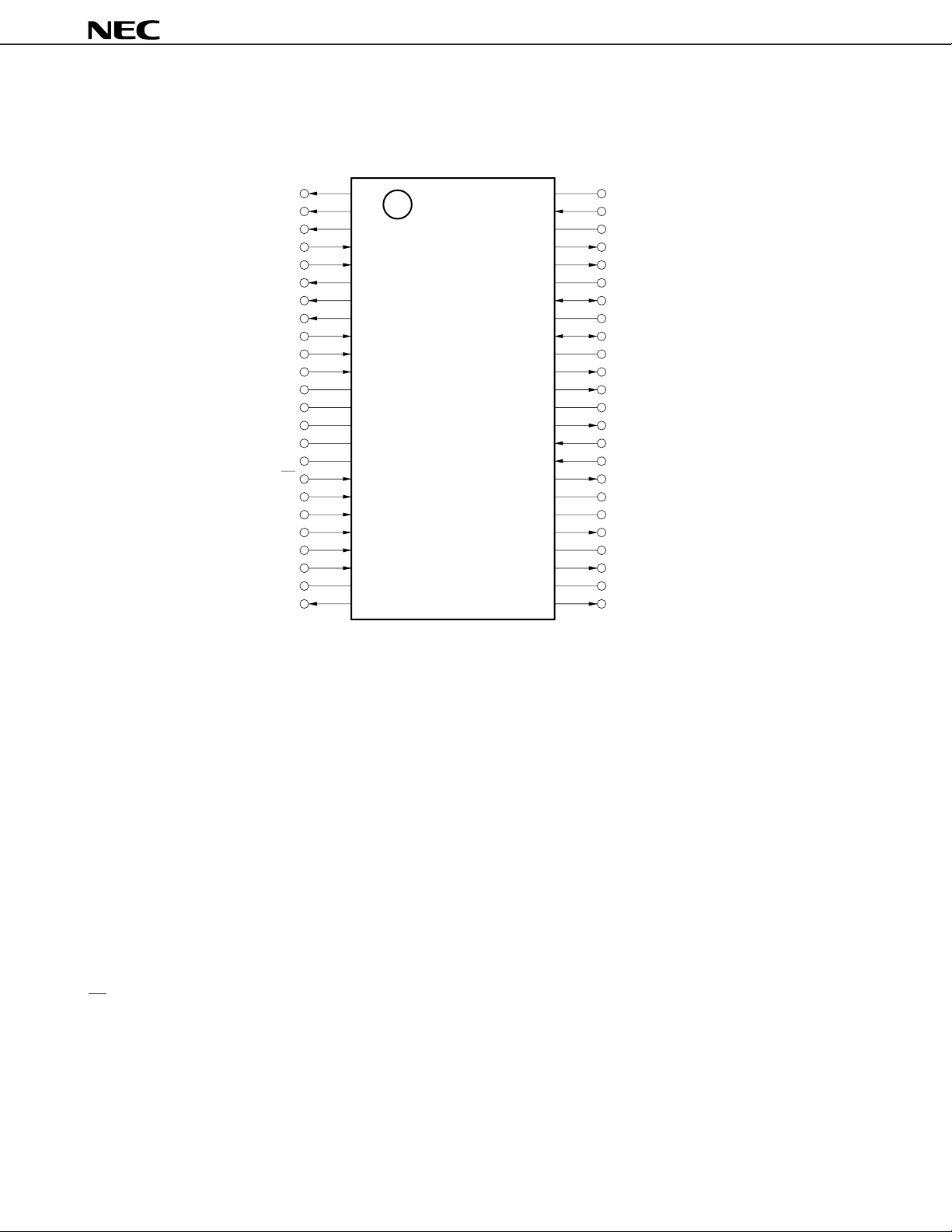
PIN CONFIGURATION
48-pin plastic shrink SOP (375 mil)
DC
OUT3
DC
OUT2
DC
OUT1
DC
IN1
DC
IN2
BB
OUT
ASCN
AGDT
BIAS
R
X
ACOM
NC
NC
NC
GND1
NC
PD
ALM
BCUT
1
RC
RC
2
RC
3
V
BB
T
EF
1
2
3
4
5
6
7
8
9
10
11
12
13
14
15
16
17
18
19
20
21
22
23
24
µ
PD7073GT
48
47
46
45
44
43
42
41
40
39
38
37
36
35
34
33
32
31
30
29
28
27
26
25
V
CC
TTX
C
PSR
R
B
R
E
NC
S
R
NC
T
S
NC
E
T
T
B
C
DC
T
X
OP
IN–
OP
IN+
R
EF
GND2
NC
3
RY
NC
2
RY
NC
1
RY
µ
PC7073
IN
ACOM : ANALOG COMMON VOLTAGE RB : RING BASE
AGDT : ANALOG GROUND DETECTION SIGNAL OUT RC
1-RC3 : RELAY CONTROL IN
ALM : ALARM IN RE : RING EMITTER
ASCN : ANALOG LOOP DETECTION SIGNAL OUT REF : RING EMITTER PROTECT FEED
OUT :VBB VOLTAGE INFORMATION OUT RS : RING SENSE
BB
BCUT : BATTERY FEED CUT SIGNAL IN RX : SIGNAL RECEPTION IN
BIAS : BIAS LEVEL RY1-RY3 : RELAY DRIVER OUT
CDC : DC FEEDBACK CAPACITOR T
B : TIP BASE
CPSR : POWER SUPPLY REJECTION CAPACITOR TE : TIP EMITTER
DCIN1, DCIN2 : DC FEEDBACK CONTROL IN TEF : TIP EMITTER PROJECT FEED
OUT1-DCOUT3 : DC FEEDBACK CONTROL OUT TS : TIP SENSE
DC
GND1, GND2 : GROUND TTXIN : TELETAX SIGNAL IN
NC : NO CONNECTION TX : TRANSSMISSION OUTPUT
IN+ : TELETAX SIGNAL CANCEL IN (+) VBB :
OP
NEGATIVE POWER SUPPLY (–48 V)
OPIN– : TELETAX SINGAL CANCEL IN (–) VCC : POSITIVE POWER SUPPLY (+5 V)
PD : POWER DOWN CONTROL IN
2

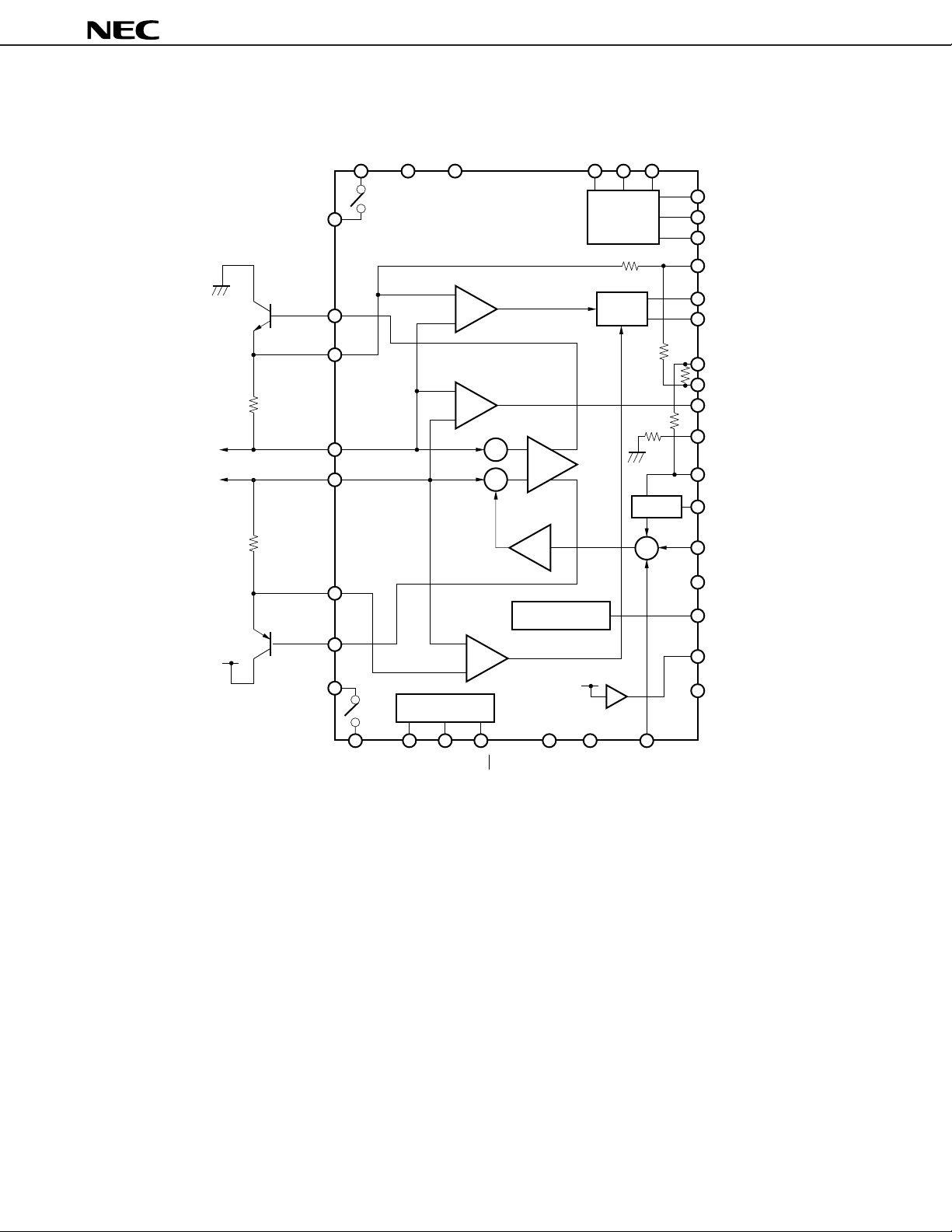
BLOCK DIAGRAM
µ
PC7073
RY
3
RY
2
RY
GND2V
GND1
T
EF
CC
1
Relay
drivers
RC
RC
RC
DC
1
2
3
OUT2
Tip
Ring
T
B
T
E
T
S
R
S
+
+
Σ
L.P.F
+
R
E
Bias circuit
R
B
R
V
BB
EF
V
BB
AGDT
ASCN
DC
OUT3
DC
OUT1
T
X
DC
IN1
DC
IN2
CDC
R
X
BIAS
ACOM
BB
OUT
C
PSR
Logic circuits
V
BB
BCUT
ALM
PD
OP
IN–OPIN+
TTX
IN
3

µ
PC7073
CONTENTS
1. PIN FUNCTIONS ............................................................................................................................. 5
2. USE CAUTIONS.............................................................................................................................. 7
3. ELECTRICAL SPECIFICATIONS ................................................................................................... 8
3.1 Discrete unit ratings............................................................................................................................... 8
3.2 Combined specifications with µPD9903 .............................................................................................. 10
4. SYSTEM APPLICATION EXAMPLE USING µPC7073 AND µPD9903 .................................... 14
5. PACKAGE DRAWING ..................................................................................................................... 15
6. RECOMMENDED SOLDERING CONDITIONS ............................................................................ 16
4

µ
PC7073
1. PIN FUNCTIONS
Number Pin Name I/O Function
1-3 DCOUT1-DCOUT3 O DC feedback control output [to the µPD9903’s pin 48-46]
4, 5 DCIN1, DCIN2 I DC feedback control input [to the µPD9903’s pin 45, 44]
6BBOUT OVBB voltage information output [to the µPD9903’s pin 43]
7 ASCN O Tip-Ring difference current detection signal output [to the µPD9903’s pin 42]
8 AGDT O Tip-Ring sum current detection signal output [to the µPD9903’s pin 41]
9 BIAS I Bias level input. Connect to µPD9903’s AIN pin [to the µPD9903’s pin 40]
10 RX I Receiving input for 4W side [to the µPD9903’s pin 39]
11 ACOM I
12-14, 16, NC – No-connection pins. Leave these pins unconnected.
26, 28, 30,
39, 41, 43
15 GND1 – Ground pin 1, for circuit grounding
17 PD I Power-down control
18 ALM I Ground-fault/power line contact protection mode select input
19 BCUT I Feed-out select input
20 RC1 I Relay control for ringer transmission, high active [to the µPD9903’s pin 29]
21 RC2 I Relay control for line test, high active [to the µPD9903’s pin 28]
22 RC3 I Relay control for network test, high active [to the µPD9903’s pin 27]
23 VBB – Negative power supply (–48 V)
24 TEF O Feed resistor pin connection for Tip side during ground-fault/power line contact
25 RY1 O Relay control for ringer transmission, open collector
27 RY2 O Relay control for line testing, open collector
29 RY3 O Relay control for network testing, open collector
31 GND2 – Ground pin 2, relay driver
32 REF O
33 OPIN+ I TTX (Teletax) signal cancel circuit input pin (+)
34 OPIN– I TTX signal cancel circuit input pin (–)
35 TX O Transmission output for 4W side. Connect with BIAS pin via CAC capacitor.
36 CDC – Connect to DC feedback capacitor
37 TB O Tip-side auxiliary power transistor base connection pin
38 TE O Tip-side feed amplifier output pin. Connect with TS pin via RFT resistor.
40 TS I/O Tip pin for 2W side
42 RS I/O Ring pin for 2W side
Signal reference voltage (2.4 V TYP) input for 4W side
H: Power-up
L: Power-down [to the µPD9903’s pin 32]
H: Protect mode
L: Normal feed [to the µPD9903’s pin 31]
H: Feed-out
L: Normal feed [to the µPD9903’s pin 30]
detection
Ring feed resistor pin connection for ground-fault/power line contact detection
Connect CDC capacitor to this pin
TTL level
TTL level
TTL level
[to the µPD9903’s pin 37, 38]
5

Number Pin Name I/O Function
44 RE O Ring-side feed amplifier output pin. Connect with RS pin via RFR resistor.
45 RB O Ring-side auxiliary power transistor base connection pin
46 CPSR – Connect a capacitor for power supply noise eliminator
47 TTXIN I TTX signal input pin
48 VCC – Positive power supply (+5 V)
µ
PC7073
6
 Loading...