NEC UPC3215TB, UPC3215TB-E3 Datasheet

PRELIMINARY DATA SHEET
BIPOLAR ANALOG INTEGRATED CI RCUIT
µµµµ
PC3215TB
5 V, SUPER MINIMOLD SILICON MMIC WIDEBAND AMPLIFIER
DESCRIPTION
The µPC3215TB is a silicon monolithic IC designed as wideband amplifier. The µPC3215TB is suitable to
systems required wideband operation from HF to L band.
This IC is manufactured using NEC’s 30 GHz f
The package is 6-pin super minimold suitable for surface mount.
FEATURES
• Wideband response : fu = 2.9 GHz TYP. @3 dB bandwidth
• Noise figure : NF = 2.3 dB TYP. @f = 1.5 GHz
• Power gain : GP = 20.5 dB TYP. @f = 1.5 GHz
• Supply voltage : VCC = 4.5 to 5.5 V
• High-density surface mounting: 6-pin super minimold package
max
UHS0 (Ultra High Speed Process) silicon bipolar process.
APPLICATION
• Systems required wideband operation from HF to L band
ORDERING INFORMATION
Part Number Package Marking Supplying Form
µ
PC3215TB-E3 6-pin super minimold C3H Embossed tape 8 mm wide.
1, 2, 3 pins face the perforat i on side of the tape.
Qty 3 kpcs/reel.
Remark
To order evaluation samples, please contact your local NEC sales office. (Part number for sample
order:
PC3215TB)
µ
Caution Electro-static sensitive devices
The information in this document is subject to change without notice. Before using this document, please
confirm that this is the latest version.
Not all devices/types available in every country. Please check with local NEC representative for
availability and additional information.
Document No. P14765EJ1V0DS00 (1st edition)
Date Published April 2000 N CP(K)
Printed in Japan
©
2000

PIN CONNECTIONS
µµµµ
PC3215TB
3
2
1
(Top View)
4
5
6
C3H
(Bottom View)
4
5
6
3
2
1
PRODUCT LINE-UP OF 5V-BIAS SILICON MMIC WIDEBAND AMPLIFIERS
A
(T
= +25 °C, VCC = 5.0 V, ZS = ZL = 50
u
Part No.
PC2711T 6-pin minimold
µ
PC2711TB
µ
PC2712T 6-pin minimold
µ
PC2712TB
µ
PC3210TB 2.3 +3.5 20 3.4
µ
PC3215TB 2.9 +3.5 20.5 2.3
µ
f
(GHz)
2.9 +1.0 13 5.0
2.6 +3.0 20 4.5
O (sat)
P
(dBm)
ΩΩΩΩ
G
(dB)
)
P
NF
(dB)
@f = 1 GHz
@f = 1 GHz
@f = 1.5 GHz
@f = 1.5 GHz
CC
I
(mA)
12
6-pin super minimold
12
6-pin super minimold
15 6-pin super minimold C2X
14 6-pin super minimold C3H
Package Marking
Pin No. Pin Name
1 INPUT
2GND
3GND
4OUTPUT
5GND
6V
CC
C1G
C1H
Remark
Typical performance. Please refer to ELECTRICAL CHARACTERISTICS in detail.
Caution The package size distinguishes between minimold and super minimold.
2
Preliminary Data Sheet P14765EJ1V0DS00

PIN EXPLANATION
µµµµ
PC3215TB
Pin
Pin Name
No.
1 INPUT
GND 0
2
Applied
Voltage
(V)
3
5
4OUTPUT
6VCC4.5 to 5.5
Pin
Voltage
Note
(V)
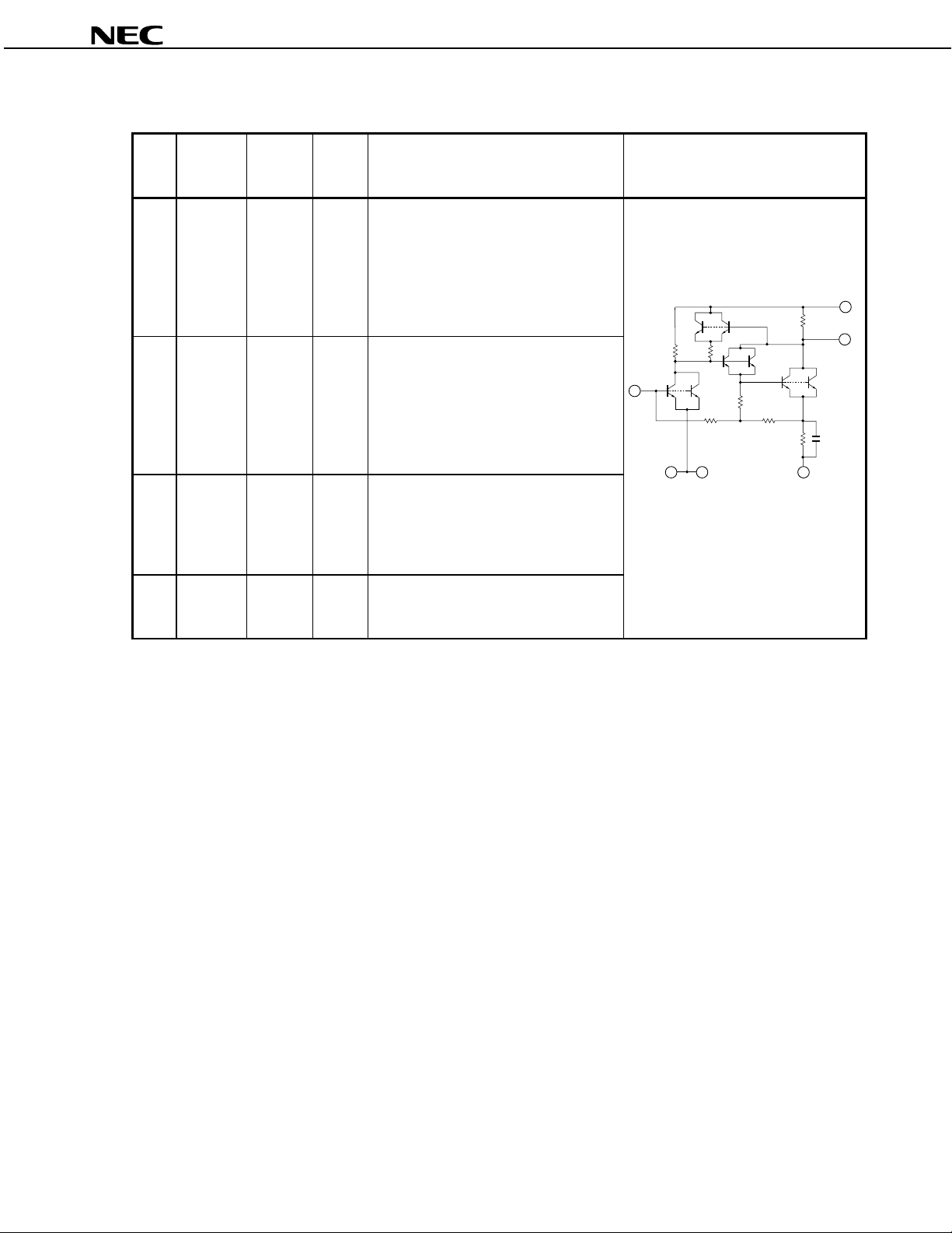
Function and Applications Internal Equivalent Circ ui t
0.82 Signal input pin. A internal m atching circuit,
configured with resistors, enables 50
Ω
connection over a wideband. A mul tifeedback circuit is designed to cancel the
deviations of h
FE
and resistance. This pin
must be coupled to signal source with
capacitor for DC cut.
Ground pin. This pin should be connect ed
to system ground with minimum inductance.
Ground pattern on the board should be
formed as wide as possible. All the ground
pins must be connected t ogether with wide
ground pattern to decrease impedance
difference.
3.8 Signal output pin. A internal matching
circuit, configured wi th resistors, enables 50
connection over a wideband. This pi n
Ω
must be coupled to next s tage with
capacitor for DC cut.
Power supply pin. This pin s houl d be
externally equipped with bypas s capacitor to
minimize ground impedance.
CC
V
6
4
OUT
IN
1
2
GND
5
3
GND
Pin voltage is measured at V
Note
CC
= 5.0 V
Preliminary Data Sheet P14765EJ1V0DS00
3
 Loading...