


NEC UPC3210TB-E3, UPC3210TB Datasheet
DATA SHEET
BIPOLAR ANALOG INTEGRATED CI RCUIT
µµµµ
PC3210TB
5 V, SUPER MINIMOLD SILICON MMIC WIDEBAND AMPLIFIER
DESCRIPTION
The µPC3210TB is a silicon monolithic integrated circuits designed as wideband amplifier. The µPC3210TB is
suitable to systems required wideband operation from HF to L band.
This IC is manufactured using NEC’s 20 GHz fT NESAT™III silicon bipolar process. This process uses silicon
nitride passivation film and gold electrodes. These materials can protect chip surface from external pollution and
prevent corrosion/migration. Thus, this IC has excellent performance, uniformity and reliability.
FEATURES
• High-density surface mounting: 6-pin super minimold package
• Supply voltage : VCC = 4.5 to 5.5 V
• Wideband response : fu = 2.3 GHz TYP. @3 dB bandwidth
• Power gain : GP = 20 dB TYP. @f = 1.5 GHz
• Noise figure : NF = 3.4 dB TYP. @f = 1.5 GHz
APPLICATION
• Systems required wideband operation from HF to 2.0 GHz
ORDERING INFORMATION
Part Number Package Marking Supplying Form
µ
PC3210TB-E3 6-pin super minimold C2X Embossed tape 8 mm wide.
1, 2, 3 pins face to perforat i on side of the tape.
Qty 3 kp/reel.
Remark
To order evaluation samples, please contact your local NEC sales office. (Part number for sample
order:
PC3210TB)
µ
Caution Electro-static sensitive devices
The information in this document is subject to change without notice. Before using this document, please
confirm that this is the latest version.
Not all devices/types available in every country. Please check with local NEC representative for
availability and additional information.
Document No. P13593EJ2V0DS00 (2nd edition)
Date Published May 1999 N CP(K)
Printed in Japan
The mark shows major revised points.
©
1998, 1999
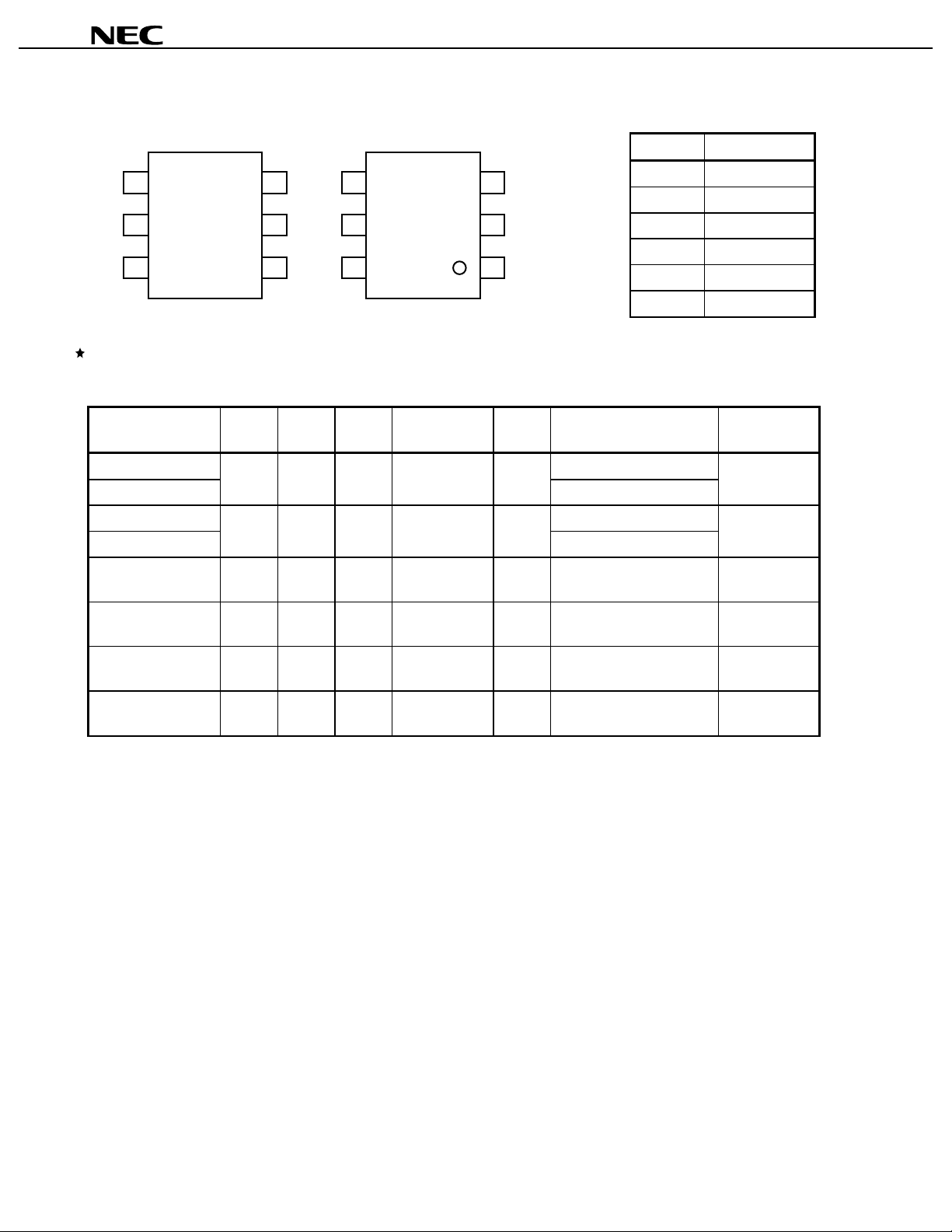
PIN CONNECTIONS
µµµµ
PC3210TB
3
2
1
(Top View)
4
5
6
C2X
(Bottom View)
4
5
6
3
2
1
PRODUCT LINE-UP OF 5V-BIAS SILICON MMIC WIDEBAND AMPLIFIERS
A
= +25 °C, VCC = 5.0 V, ZL = ZS = 50
(T
u
Part No.
PC2711T 6-pin minimold
µ
PC2711TB
µ
PC2712T 6-pin minimold
µ
PC2712TB
µ
PC2713T 1.2 +7.0 29 3.2
µ
PC2791TB 1.9 +4.0 12 5.5
µ
PC2792TB 1.2 +5.0 20 3.5
µ
PC3210TB 2.3 +3.5 20 3.4
µ
f
(GHz)
2.9 +1.0 13 5.0
2.6 +3.0 20 4.5
O (sat)
P
(dBm)
ΩΩΩΩ
G
(dB)
)
P
NF
(dB)
@f = 1 GHz
@f = 1 GHz
@f = 0.5 GHz
@f = 0.5 GHz
@f = 0.5 GHz
@f = 1.5 GHz
CC
I
(mA)
12
6-pin super minimold
12
6-pin super minimold
12 6-pin minimold C1J
17 6-pin super minimold C2S
19 6-pin super minimold C2T
15 6-pin super minimold C2X
Package Marking
Pin No. Pin Name
1 INPUT
2GND
3GND
4OUTPUT
5GND
6V
CC
C1G
C1H
Remark
Notice
2
Typical performance. Please refer to ELECTRICAL CHARACTERISTICS in detail.
The package size distinguishes between minimold and super minimold.
Data Sheet P13593EJ2V0DS00
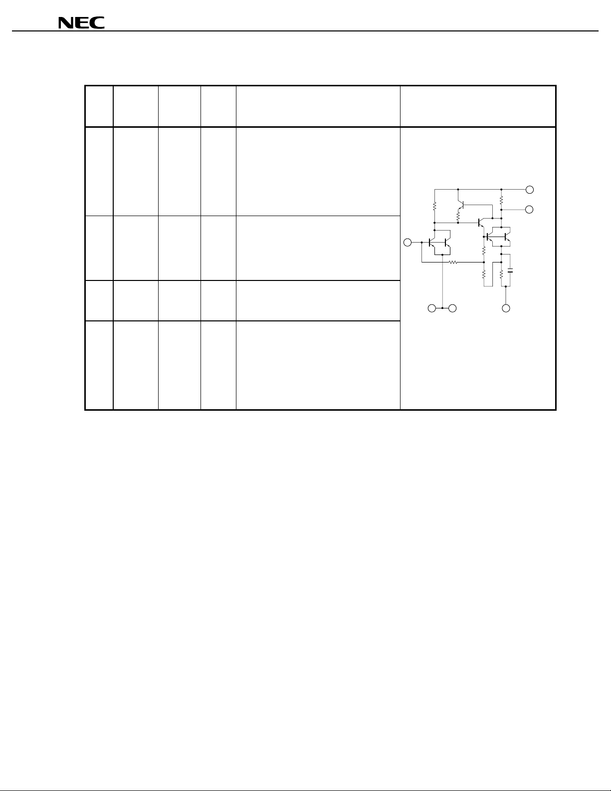
PIN EXPLANATION
µµµµ
PC3210TB
Pin
Pin Name
No.
1 INPUT
4OUTPUT
Applied
Voltage
V
6VCC4.5 to 5.5
2
GND 0
3
5
Pin
Voltage
Note
V
Function and Applications Internal Equivalent Circ ui t
0.82 Signal input pin. A internal m atching circuit,
configured with resistors, enables 50
Ω
connection over a wide band. A mul tifeedback circuit is designed to cancel the
FE
deviations of h
and resistance. This pin
must be coupled to signal source with
capacitor for DC cut.
4.0 Signal output pin. A internal matching
circuit, configured wi th resistors, enables 50
connection over a wide band. This pi n
Ω
must be coupled to next s tage with
capacitor for DC cut.
Power supply pin. This pin s houl d be
externally equipped with bypas s capacitor to
minimize ground impedance.
Ground pin. This pin should be connect ed
to system ground with minimum inductance.
Ground pattern on the board should be
formed as wide as possible. All the ground
pins must be connected t ogether with wide
ground pattern to decrease impedance
difference.
1
IN
2
GND GND
V
CC
6
4
OUT
5
3
Pin voltage is measured at V
Note
CC
= 5.0 V
Data Sheet P13593EJ2V0DS00
3
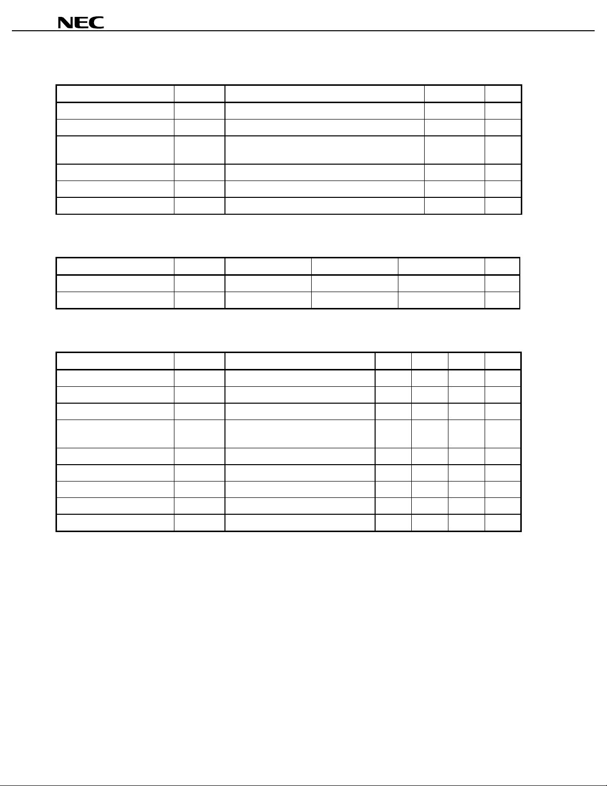
ABSOLUTE MAXIMUM RATINGS
Parameter Symbol Conditions Ratings Unit
µµµµ
PC3210TB
Supply Voltage V
Circuit Current I
Total Power Dissipat i on P
Operating Ambient Temperature
Storage Temperature T
Input Power Level P
CC
CC
D
A
T
stg
in
TA = +25 °C 6.0 V
TA = +25 °C 30 mA
Mounted on double sided copper clad
50 × 50 × 1.6 mm epoxy glass P WB (T
A
= +85 °C)
200 mW
–40 to +85 °C
–55 to +150 °C
TA = +25 °C +10 dBm
RECOMMENDED OPERATING CONDITIONS
Parameter Symbol MIN. TYP. MAX. Unit
T
CC
f
O (sat)
G
∆
CC
A
4.5 5.0 5.5 V
–40 +25 +85 °C
)
ΩΩΩΩ
No signals 11.5 15.0 19.5 mA
P
u
f = 1.5 GHz 18 20 – dB
3 dB down below from gain at
2.05 2.3 – GHz
f = 0.1 GHz
in
f = 1.5 GHz 10 14.5 – dB
out
f = 1.5 GHz 7 11 – dB
f = 1.5 GHz, Pin = 0 dBm +0.5 +3.5 – dBm
P
f = 0.1 GHz to 2.05 GHz –
1.0 – dB
±
Supply Voltage V
Operating Ambient Temperature
ELECTRICAL OPERATING CONDITIONS (TA = +25°C, VCC = 5.0 V, ZS = ZL = 50
Parameter Symbol Test Conditions MIN. TYP. MAX. Unit
Circuit Current I
Power Gain G
Noise Figure NF f = 1.5 GHz – 3.4 4.4 dB
Upper Limit Operating
Frequency
Isolation ISL f = 1.5 GHz 29 34 – dB
Input Return Loss RL
Output Return Loss RL
Maximum Output Level P
Gain Flatness
4
Data Sheet P13593EJ2V0DS00
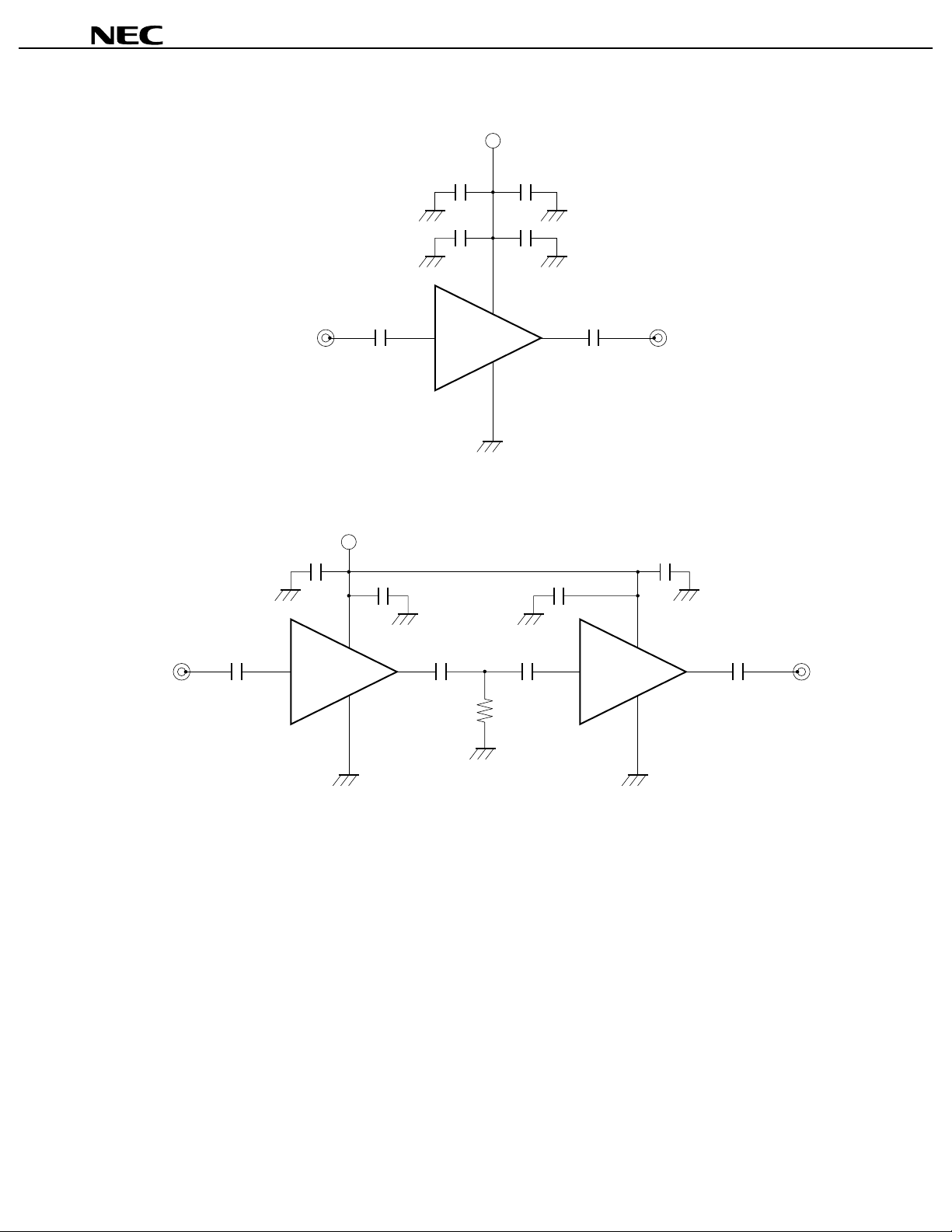
TEST CIRCUIT
V
CC
1 000 pF 1 000 pF
C
4
C
3
C
6
C
5
1 000 pF 1 000 pF
6
µµµµ
PC3210TB
50 Ω
1
C
IN
1 000 pF
EXAMPLE OF APPLICATION CIRCUIT
V
CC
1 000 pF
C
4
IN
C
3
6
50 Ω
1
C
1
1 000 pF 1 000 pF
2, 3, 5
1
4
1 000 pF
C
1 000 pF
2
C
4
50 Ω
OUT
1 000 pF
2, 3, 5
1 000 pF
C
1 000 pF
5
C
6
6
7
8
C
1
C
4
50 Ω
2
OUT
1 000 pF
R
1
50 to 200 Ω
To stabilize operation,
please connect R
1
, C
2, 3, 5
8
The application circuits and their parameters are for reference only and are not intended for use in actual design-ins.
Capacitors for VCC, input and output pins
CC
1 000 pF capacitors are recommendable as bypass capacitor for V
pin and coupling capacitors for input/output
pins.
Bypass capacitor for VCC pin is intended to minimize VCC pin’s ground impedance. Therefore, stable bias can be
supplied against VCC fluctuation.
Coupling capacitors for input/output pins are intended to minimize RF serial impedance and cut DC.
To get flat gain from 100 MHz up, 1 000 pF capacitors are assembled on the test circuit. [Actually, 1 000 pF
capacitors give flat gain at least 10 MHz. In the case of under 10 MHz operation, increase the value of coupling
capacitor such as 2 200 pF. Because the coupling capacitors are determined by the equation of C = 1/(2 π fZs).]
Data Sheet P13593EJ2V0DS00
5