NEC UPC3206GR-E1, UPC3206GR Datasheet

DATA SHEET
DATA SHEET
BIPOLAR ANALOG INTEGRATED CI RCUIT
µµµµ
PC3206GR
50dB AGC AMP + VIDEO AMP
DESCRIPTION
The µPC3206GR is Silicon monolithic IC designed for Digital DBS and Digital CATV receivers. This IC consists of
a two stage gain control amplifier and a wideband linear video amplifier.
This IC is packaged in 20-pin SSOP. Therefore, it can make RF block small.
FEATURES
• Broadband AGC dynamic range 50 dB (MIN.)
• Supply voltage 5 V
• Packaged in 20-pin SSOP suitable for high-density surface mount
APPLICATIONS
• Digital DBS receiver
• STB of digital CATV
ORDERING INFORMATION
Part Number Package Supplying Form
µ
PC3206GR-E1 20-pin plastic SSOP
(225 mil)
To order evaluation samples, please contact your local NEC office. (Part number for sample order : µPC3206GR)
Embossed tape 12 mm wide.
Pin 1 indicates pull-out di rection of tape.
Qty 2.5 kp/reel.
The information in this document is subject to change without notice. Before using this document, please
confirm that this is the latest version.
Not all devices/types available in every country. Please check with local NEC representative for
availability and additional information.
Document No. P13710EJ3V0DS00 (3rd edition)
Date Published October 1999 N CP(K)
Printed in Japan
Caution electro-static sensitive device
The mark shows major revised points.
1998, 1999©
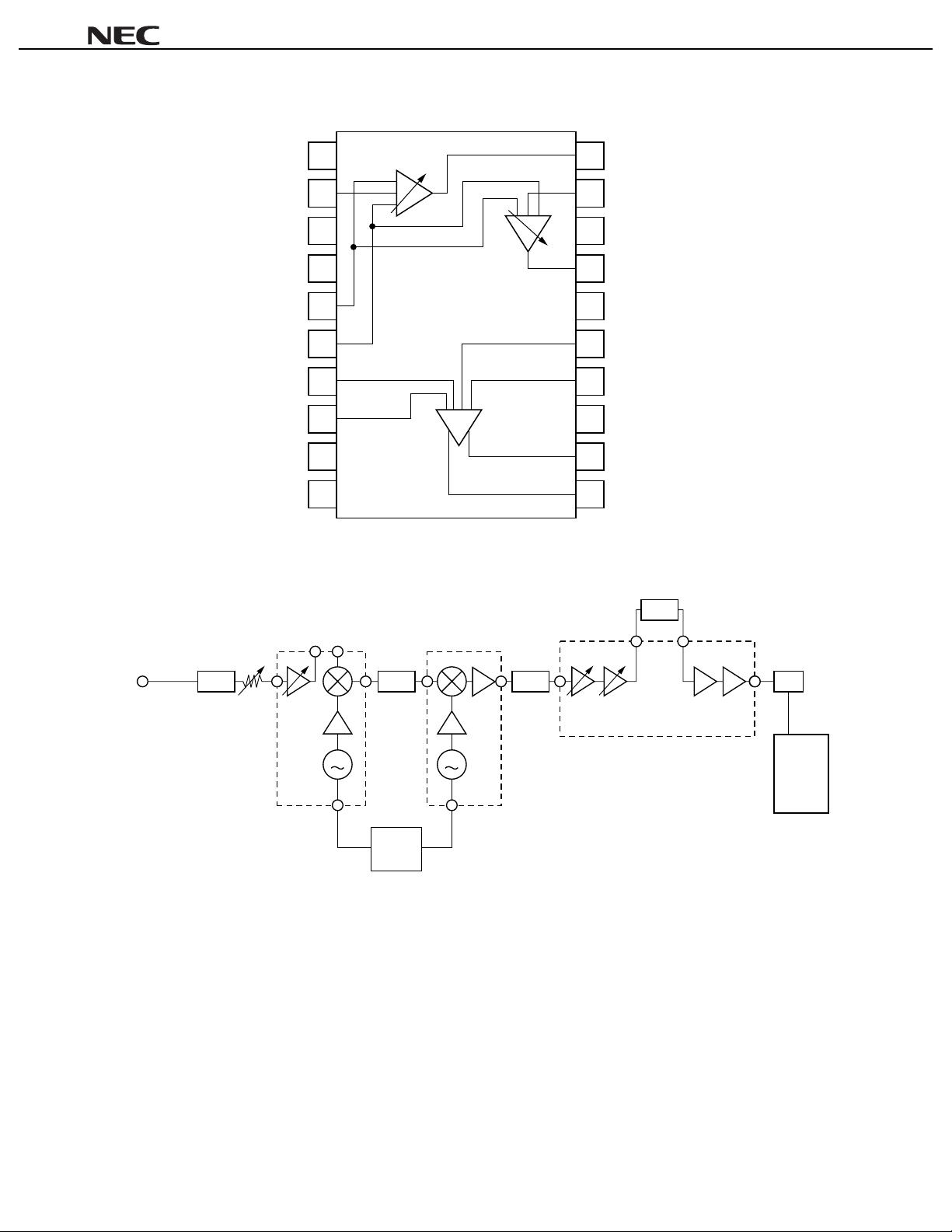
INTERNAL BLOCK DIAGRAM AND PIN CONFIGULATION (Top View)
µµµµ
PC3206GR
AGC GND1 20 AGC OUT1
TYPICAL APPLICATION
1 AGC Amp1
2AGC IN1 19 AGC IN2
3V
AGC 18 AGC VCC1
4AGC V
CC1 17 AGC OUT2
AGC Amp2
5BPCAP 16 AGC GND2
6BPCAP 15 INA
7G1A 14 INB
8G1B 13 VAMP V
CC2
VIDEO
9VAMP GND1 12 VAMP OUT1
Amp
10VAMP GND2 11 VAMP OUT2
RF IN
µ
PC2799GR
1st IF
HPF SAW
DUAL
PLL
PC1686GV
µ
PC3206GR
µ
2nd IF
SAW A/D
LPF
Video Amp.
QAM
Demo.
&FEC
2
Data Sheet P13710EJ3V0DS00
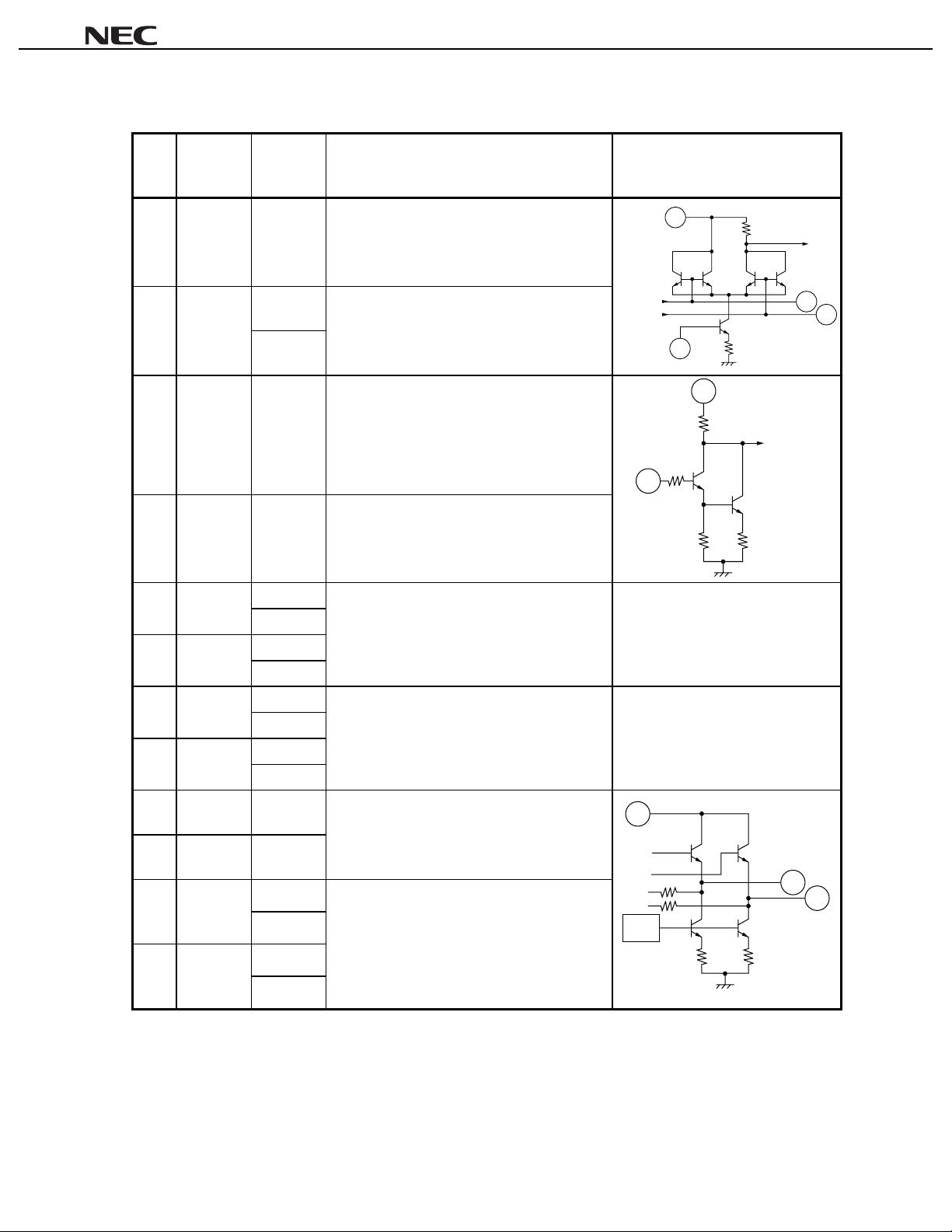
PIN FUNCTIONS
µµµµ
PC3206GR
Pin
Pin Name
No.
1AGC
GND1
Pin
Voltage
Function and Explanation Equivalent Circuit
TYP.(V)
0 Ground pin of AGC amplifier1.
Form a ground pattern as wide as possi bl e t o
maintain the minimum im pedance.
2 AGC IN 1
Note 1
1.02
Signal input pin to AGC ampli f i er.
1.02
3 VAGC 0 to 5 Gain control pin.
This pin’s bias govern the A G C out put level.
Minimum gain at V
Maximum gain at V
AGC
AGC
= 0 V
= 5 V
Recommended to use by dividi ng AGC voltage
with externally resis tor (ex.100 kΩ).
4AGC VCC1 5 Power supply pin of AGC ampli f i er1.
Must be connected bypass capacitor to
minimize ground impedance.
Note 1
2.615 BPCAP4
Bypass pin of AGC ampli fier1 and 2. Refer to Equivalent circui t of pin1 and
2.61
Note 1
2.846 BPCAP2
2.49
Note 2
G1A
G1B
9 VAMP
GND1
10 VAMP
GND2
11 VAMP
OUT2
Note 2
Note 2
1.727
3.34
1.728
3.34
0
0
2.52
4.92
Gain control pin of video ampli fier.
Maximum gain at G1A – G1B = s hort .
Minimum gain at G1A – G1B = open.
Gain is able to adjust by i ns erting arbitrary
resistor between 7pin and 8pin.
Ground pin of video amplifier.
Form a ground pattern as wide as possi bl e t o
maintain the minimum im pedance.
Signal output pin of video ampl i fier.
In case of R
equal 2V
L
= 1 kΩ, single-end output voltage
P-P
.
4
AGC
Control
2
4
AGC
Control
3
pin2.
Refer to Equivalent circuit of pin14
and pin15.
13
12
REG
5
6
11
12 VAMP
OUT1
Notes 1.
2.
2.52
Note 2
above : V
4.92
AGC
= VCC1 below : V
AGC
= 0 V
above : VCC2 = 5 V below : VCC2 = 9 V
Data Sheet P13710EJ3V0DS00
3
µµµµ
PC3206GR
Pin
Pin Name
No.
13 VAMP
CC
V
2
Pin
Voltage
Function and Explanation Equivalent Circuit
TYP.(V)
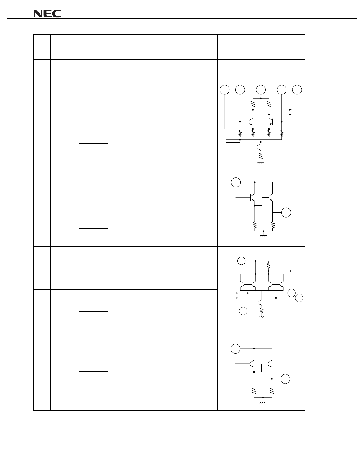
5 to 9 Power supply pin of video ampl i f i er.
Must be connected bypass capacitor to
minimize ground impedance.
14
INB
Note 2
2.49
Signal input pin to video ampl i f i er.
4.13
Note 2
INA
15
2.49
4.13
16 AGC GND2 0 Ground pin of AGC amplifier2.
Form a ground pattern as wide as possi bl e t o
maintain the minimum im pedance.
7 81315 14
REG
18
17 AGC O U T 2
Note 1
1.69
Signal output pin of AGC ampli fier2.
3.31
18 AG C VCC1 5 Power supply pin of AGC ampli f i er2.
Must be connected bypass capacitor to
minimize ground impedance.
19 AGC IN2
Note 1
1.01
Signal input pin of AGC ampli f i er2.
1.01
20 AGC O U T 1
Note 1
Signal output pin of AGC ampli fier1.
1.71
AGC
Control
17
18
5
6
19
4
20
Notes 1.
4
3.35
AGC
above : V
above : VCC2 = 5 V below : VCC2 = 9 V
2.
= VCC1 below : V
Data Sheet P13710EJ3V0DS00
AGC
= 0 V

µµµµ
PC3206GR
ABSOLUTE MAXIMUM RATINGS (TA = 25
C unless otherwise specified)
°°°°
Parameter Symbol Conditions Rating Unit
Supply Voltage 1 VCC1
Supply Voltage 2 VCC2
AGC Control Voltage V
AGC
MIXER Block
Video Amp Block
6.0 V
6.0 V
6.0 V
Maximum Input Power Pin (MAX.) +10 dBm
Power Dissipation P
Operating Ambient Temperature T
Storage Temperature T
D
A
stg
TA = 85 °C
Note
433 mW
–40 to +85
–55 to +150
Parameter Symbol Conditions Rating Unit
Supply Voltage 1 VCC1
Supply Voltage 2 VCC2
AGC Control Voltage V
AGC
MIXER Block
Video Amp Block
6.0 V
11.0 V
6.0 V
Maximum Input Power Pin (MAX.) +10 dBm
Power Dissipation P
Operating Ambient Temperature T
Storage Temperature T
D
A
stg
TA = 75 °C
Note
500 mW
–40 to +75
–55 to +150
C
°
C
°
C
°
C
°
Mounted on 50 × 50 × 1.6 mm double epoxy glass board.
Note
RECOMMENDED OPERATING RANGE
Parameter Symbol
Supply Voltage 1 VCC1
Supply Voltage 2 VCC2
Operating Ambient Temperature 1
Operating Ambient Temperature 2
CC
1 = VCC2 = 4.5 to 5.5 V
Notes 1.
V
VCC1 = 4.5 to 5.5 V, VCC2 = 4.5 to 10 V
2.
Note 1
Note 2
TA1
TA2
MIN. TYP. MAX. Unit
4.5 5.0 5.5 V
4.5 9.0 10.0 V
–40 +25 +85
–40 +25 +75
°
°
C
C
Data Sheet P13710EJ3V0DS00
5

µµµµ
PC3206GR
ELECTRICAL CHARACTERISTICS (TA = 25
C)
°°°°
Parameter Symbol Test Conditions MIN. TYP. MAX. Unit
AGC Amplifier Block (VCC1 = 5 V, fin = 100 MHz, RL = 560 Ω)
AGC
, V
AGC
AGC
AGC
AGC
AGC
AGC
= 0 V),
= 5 V
= 0 V
= 5 V),
= 5 V
= 0 V
= 0 to 5V
Note 1
Note 1
Note 2, 3
Note 3
Note 3
Note 3
Note 3
Note 3
Circuit Current 1 ICC1
Circuit Current 2 ICC2
no input signal, V
no input signal, V
Bandwidth 1 BW1 Maximum gain (V
Pin = –60 dBm
Bandwidth 2 BW2 Minimum gain (V
Pin = –15 dBm
MIN
1
2
Pin = –60 dBm, V
Pin = –15 dBm, V
Pin = –35 dBm
AGC
V
= 5 V, Pin = 0 dBm
Maximum Gain 1 G
MAX
Minimum Gain 1 G
Gain Control Range GCR
Maximum Output Power P
o (sat)
Video Amplifier Bloc k (VCC2 = 9 V, fin = 100 MHz, RL = 1 kΩ)
Circuit Current 3 ICC3
Differential Gain 1 G1
Differential Gain 2 G2
no input signal
G1A-G1B pins:short
G1A-G1B pins:open
Note 4
Note 5
Note 5
Video Amplifier Bloc k (VCC2 = 5 V, fin = 100 MHz, RL = 1 kΩ)
Circuit Current 4 ICC4
Differential Gain 3 G3
Differential Gain 4 G4
no input signal
G1A-G1B pins:short
G1A-G1B pins:open
Note 4
Note 5
Note 5
Video Amplifier Bloc k (VCC2 = 5 V, 9 V Common, fin = 100 MHz , RL = 1 kΩ, single-ended)
Bandwidth 1 BW
G1A-G1B pins:short
G1
Note 2, 5
11 16 22 mA
15 22 32 mA
100 220 – MHz
500 – – MHz
36 38.5 41 dB
– –28 –15 dB
50 – – dB
02–dBm
16 24 34.5 mA
160 260 400 V/V
22 25 30 V/V
8 12.5 18 mA
80 140 230 V/V
16 22 30 V/V
– 100 – MHz
Notes 1.
By measurement circuit 1
–3 dB down from gain at 5 MHz
2.
By measurement circuit 2
3.
By measurement circuit 3
4.
By measurement circuit 4
5.
6
Data Sheet P13710EJ3V0DS00

µµµµ
PC3206GR
STANDARD CHARACTERISTICS (FOR REFERENCE) (TA = 25
Parameter Symbol Test Conditions Reference Values Unit
AGC Amplifier Block (VCC1 = 5 V, fin = 100 MHz, RL = 560 Ω)
Noise Figure NF
Output Intercept Point OIP
Maximum Gain (V
fin2 = 106 MHz, Maximum Gain
3
AGC
(V
= 5 V)
Video Amplifier Bloc k (VCC2 = 9 V, fin = 100 MHz, RL = 1 kΩ)
Output Voltage Vout
Single-end Gain 1 Avs1
Single-end Gain 2 Avs2
Input Intercept Point 1 IIP31
single-ended
G1A-G1B pins:short
G1A-G1B pins:open
fin2 = 106 MHz,
G1A-G1B pins:short
Input Intercept Point 2 IIP32
fin2 = 106 MHz,
G1A-G1B pins:open
Video Amplifier Bloc k (VCC2 = 5 V, fin = 100 MHz, RL = 1 kΩ)
Single-end Gain 3 Avs3
Single-end Gain 4 Avs4
Input Intercept Point 3 IIP33
G1A-G1B pins:short
G1A-G1B pins:open
fin2 = 106 MHz,
G1A-G1B pins:short
Input Intercept Point 4 IIP34
fin2 = 106 MHz,
G1A-G1B pins:open
AGC
= 5 V)
C)
°°°°
Note 1
Note 2
Note 3
Note 3
Note 3
Note 3
Note 3
Note 3
Note 3
Note 3
Note 3
5.5 dB
+4.5 dBm
2V
P-P
130 V/V
12 V/V
–16 dBm
4dBm
70 V/V
11 V/V
–15 dBm
2dBm
Total Block (VCC1 = 5 V, fin = 100 MHz, RL = 1 kΩ)
Maximum Gain 2 G
Maximum Gain 3 G
Minimum Gain 2 G
Maximum Gain 4 G
Maximum Gain 5 G
Minimum Gain 3 G
Notes 1.
By measurement circuit 5
By measurement circuit 2
2.
By measurement circuit 4
3.
By measurement circuit 6
4.
MAX
MAX
MIN
MAX
MAX
MIN
2
3
2
4
5
3
AGC
V
= 5 V, VCC2 = 5 V,
G1A-G1B pins:short
AGC
V
= 5 V, VCC2 = 5 V,
G1A-G1B pins:open
AGC
V
= 0 V, VCC2 = 5 V,
G1A-G1B pins:short
AGC
V
= 5 V, VCC2 = 9 V,
G1A-G1B pins:short
AGC
V
= 5 V, VCC2 = 9 V,
G1A-G1B pins:open
AGC
V
= 0 V, VCC2 = 9 V,
G1A-G1B pins:short
76 dB
Note 4
62 dB
Note 4
10 dB
Note 4
80 dB
Note 4
63 dB
Note 4
14 dB
Note 4
Data Sheet P13710EJ3V0DS00
7
µµµµ
PC3206GR
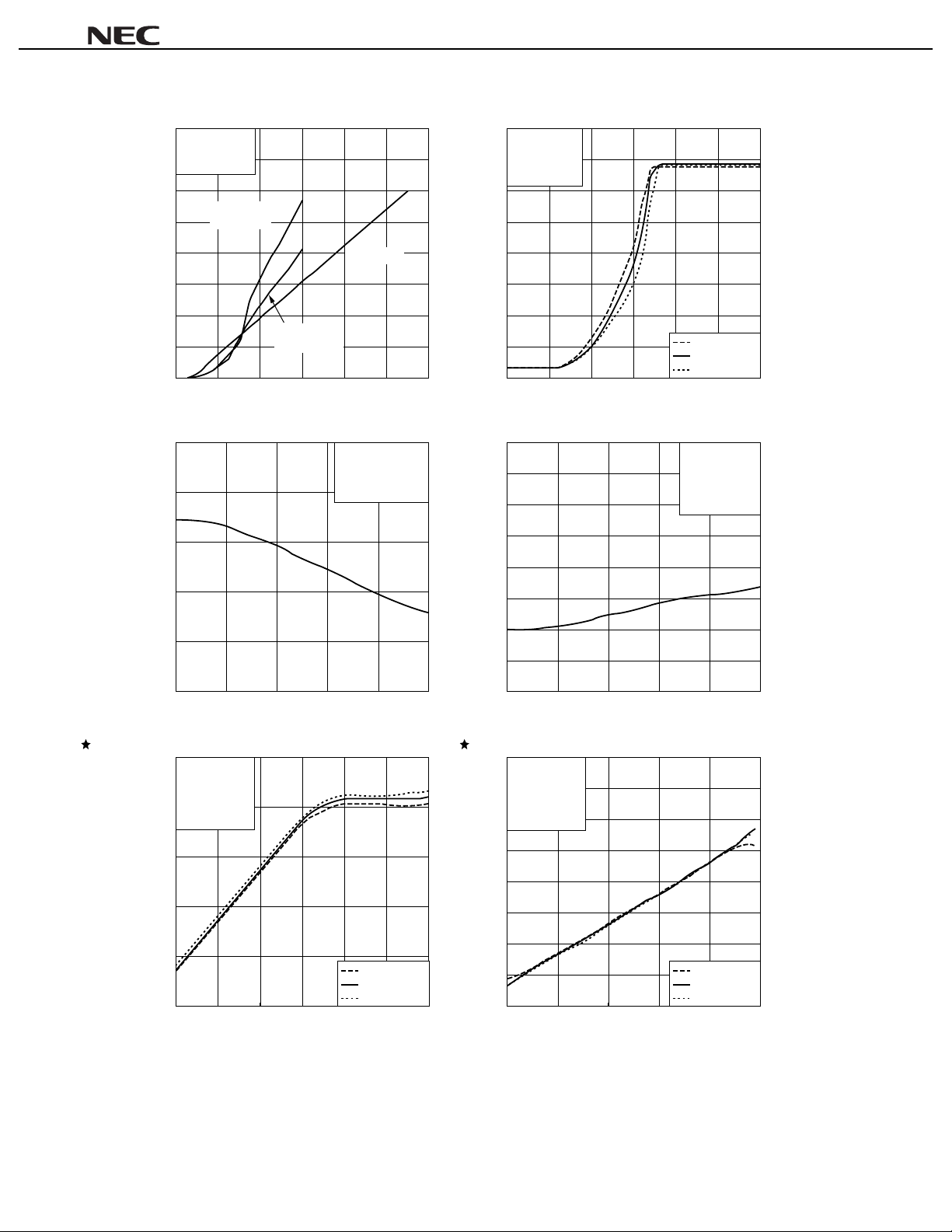
TYPICAL CHARACTERISTICS (TA = 25
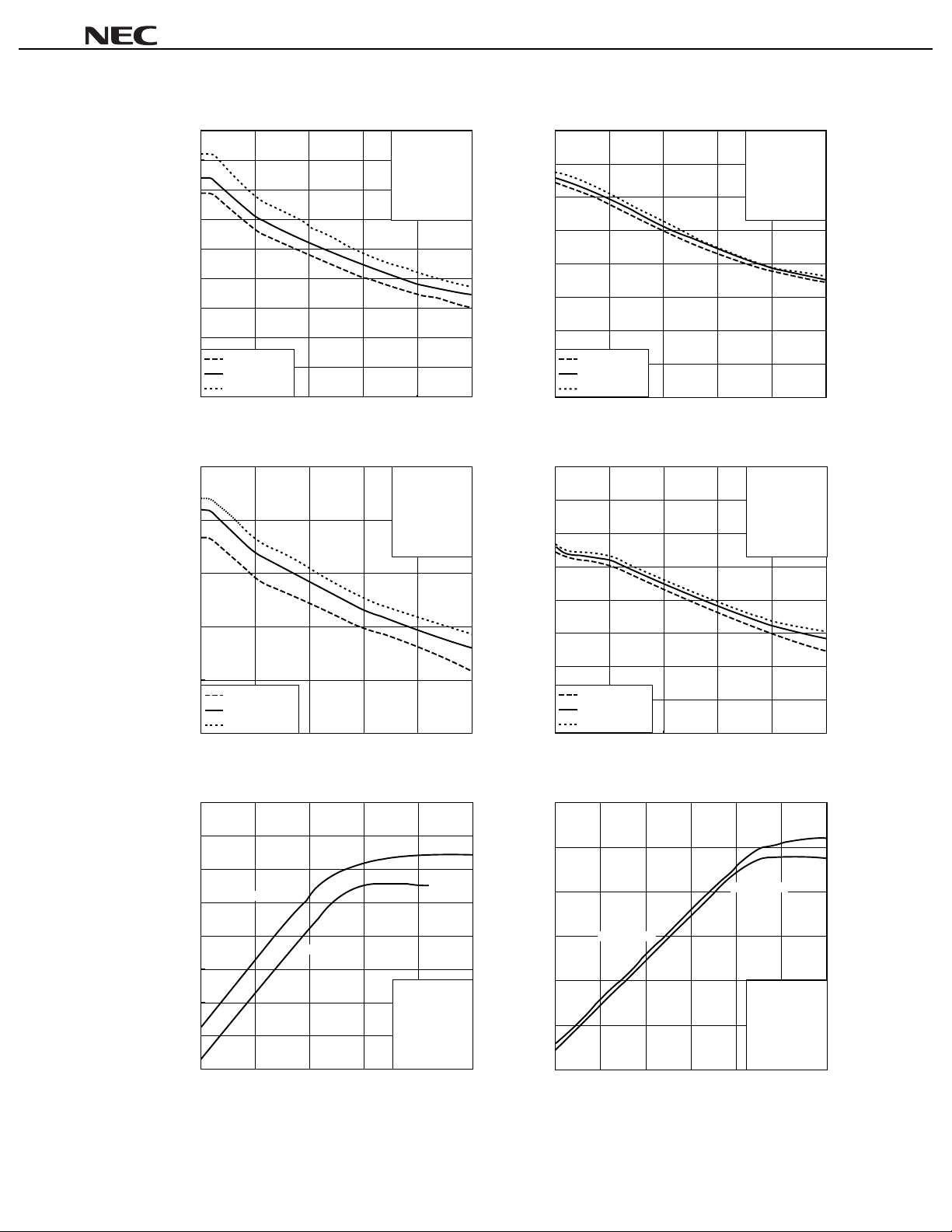
CIRCUIT CURRENT vs. SUPPLY VOLTAGE
40
No input signal
measurement
35
circuit1, 3
30
(mA)
25
CC
20
15
Circuit Current I
10
25
20
15
10
AGC
AGC
= 0 V)
(V
5
0
024
Supply Voltage V
GAIN vs. INPUT FREQUENCY
Video Amp.
AGC
AGC
= VCC1)
(V
6 8 10 12
CC
(V)
VCC1 = V
P
in
= -60 dBm
measurement
circuit2
C)
°°°°
AGC
Note1
= 5 V
50
fin = 100 MHz
L
= 560 Ω
R
40
measurement
circuit2
30
20
10
Gain (dB)
0
-
10
-
20
-
30
012
-
20
-
30
-
40
GAIN vs. INPUT FREQUENCY
GAIN vs. AGC VOLTAGE
3456
AGC
AGC Voltage V
(V)
VCC1 = 5 V
V
P
measurement
circuit2
CC
1 = 4.5 V
V
V
CC
1 = 5.0 V
CC
1 = 5.5 V
V
AGC
= 0 V
in
= -15 dBm
Note1
Gain (50 Ω/560 Ω) (dB)
5
0
0 100 200
OUTPUT POWER vs. INPUT POWER
0
V
AGC
= VCC1
in
= 100 MHz
f
L
= 560 Ω
R
-
10
measurement
Note2
circuit2
-
20
(50 Ω/560 Ω) (dBm)
out
-
30
-
40
Output Power P
-
50
-
60-50-40
Input Frequency f
Input Power P
300 400 500
in
(MHz)
VCC1 = 4.5 V
V
CC
1 = 5.0 V
CC
1 = 5.5 V
V
-
30-20-10 0
in
(dBm)
Notes 1.2.Gain = (Gain at Spectrum Analyzer) + 20 log (560 Ω/50 Ω)
Output Power = (Output Power at Spectrum Analyzer) + 10 log (560 Ω/50 Ω)
Gain (50 Ω/560 Ω) (dB)
-
50
-
60
0 100 200
-
10
-
20
-
30
-
40
-
50
(50 Ω/560 Ω) (dBm)
out
-
60
-
70
Output Power P
-
80
-
90
OUTPUT POWER vs. INPUT POWER
V
AGC
= 0 V
in
= 100 MHz
f
L
= 560 Ω
R
measurement
Note2
circuit2
-
35
-
Input Frequency f
25
-
15
Input Power P
300 400 500
in
(MHz)
VCC1 = 4.5 V
V
CC
1 = 5.0 V
CC
1 = 5.5 V
V
-
5155
in
(dBm)
8
Data Sheet P13710EJ3V0DS00
µµµµ
PC3206GR
TYPICAL CHARACTERISTICS (TA = 25
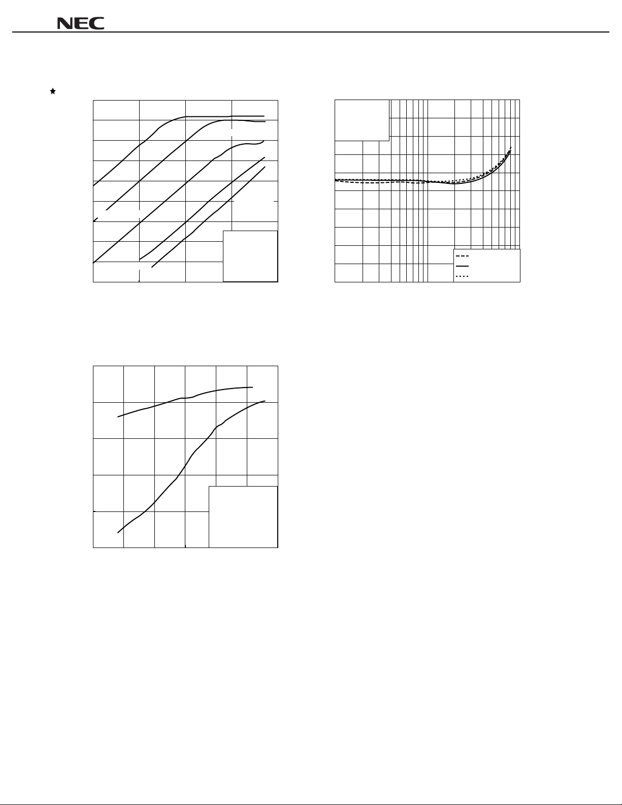
DIFFERENTIAL GAIN vs. INPUT FREQUENCY
450
400
350
(V/V)
300
video
250
200
150
Differential Gain G
100
V
CC
50
0
CC
V
CC
V
2 = 8 V
2 = 9 V
2 = 10 V
0 50 100
Input Frequency f
DIFFERENTIAL GAIN vs. INPUT FREQUENCY
250
200
(V/V)
video
150
fin = 100 MHz
L
= 1 kΩ
R
G1A-G1B
= SHORT
measurement
circuit4
150 200 250
in
(MHz)
fin = 100 MHz
L
= 1 kΩ
R
G1A-G1B
= SHORT
measurement
circuit4
C)
°°°°
DIFFERENTIAL GAIN vs. INPUT FREQUENCY
40
35
fin = 100 MHz
L
= 1 kΩ
R
G1A-G1B
= OPEN
30
(V/V)
25
video
measurement
circuit4
20
15
10
Differential Gain G
V
CC
5
0
0 50 100
40
35
2 = 8 V
CC
2 = 9 V
V
CC
2 = 10 V
V
150 200 250
Input Frequency f
in
(MHz)
DIFFERENTIAL GAIN vs. INPUT FREQUENCY
fin = 100 MHz
L
= 1 kΩ
R
G1A-G1B
= OPEN
30
(V/V)
25
video
measurement
circuit4
20
100
Differential Gain G
50
V
CC
2 = 4.5 V
CC
2 = 5.0 V
V
CC
2 = 5.5 V
V
0
0 50 100
OUTPUT POWER vs. INPUT POWER
0
-
5
-
10
) (dBm)
Ω
/1 k
-
15
Ω
(50
-
20
out
-
25
-
30
Output Power P
-
35
-
40
-
50
VCC2 = 9 V
-
40
Input Frequency f
V
CC
2 = 5 V
-
30
Input Power P
150 200 250
in
(MHz)
fin = 100 MHz
L
= 1 kΩ
R
G1A-G1B
= SHORT
measurement
Note
circuit4
-
20
in
(dBm)
-
10 0
15
10
Differential Gain G
5
0
0 50 100
0
-
10
) (dBm)
Ω
-
20
/1 k
Ω
(50
-
30
out
-
40
-
50
Output Power P
-
60
-
50
Note Output Power = (Output Power at Spectrum Analyzer) + 10 log (1 kΩ/50 Ω)
CC
2 = 4.5 V
V
CC
2 = 5.0 V
V
CC
2 = 5.5 V
V
150 200 250
Input Frequency f
in
(MHz)
OUTPUT POWER vs. INPUT POWER
VCC2 = 5 V
VCC2 = 9 V
fin = 100 MHz
R
L
= 1 kΩ
G1A-G1B
= OPEN
measurement
circuit4
-
40
-
30
-
20
-
10 0 10
Input Power P
in
(dBm)
Note
Data Sheet P13710EJ3V0DS00
9
µµµµ
PC3206GR
STANDARD CHARACTERISTICS (TA = 25
OUTPUT POWER vs. INPUT POWER
0
-
10
V
AGC
-
20
V
AGC
) (dBm)
Ω
-
30
/560
Ω
-
40
(50
out
-
50
-
60
-
70
Output Power P
-
80
-
90
= 5 V
V
AGC
= 2.8 V
V
AGC
= 2 V
-
60
-
40
Input Power P
-
20 0 20
in
(dBm)
3rd ORDER INTERMODULATION DISTORTION
0
= 3.25 V
V
AGC
VCC1 = 5 V
f
in
= 100 MHz
R
L
= 560 Ω
measurement
circuit2
C)
°°°°
= 0 V
Note
NOISE FIGURE vs. INPUT FREQUENCY
10
V
AGC
= VCC1
R
L
= 560 Ω
9
measurement
circuit5
8
7
6
5
4
3
Noise Figure NF (dB)
2
1
0
10 100
Input Frequency f
in
(MHz)
VCC1 = 4.5 V
V
CC
1 = 5.0 V
V
CC
1 = 5.5 V
1000
-
20
) (dBm)
Ω
/560
-
40
Ω
(50
out
-
60
-
80
Output Power P
-
100
-
50
-
45
-
40
-
35
Input Power P
VCC1 = V
f
f
R
measurement
circuit2
-
in
(dBm)
AGC
in
1 = 100 MHz
in
2 = 106 MHz
L
= 560 Ω
Note
30
-
25 –20
= 5 V
Note Output Power = (Output Power at Spectrum Analyzer) + 10 log (560 Ω/50 Ω)
10
Data Sheet P13710EJ3V0DS00
 Loading...