DATA SHEET
BIPOLAR ANALOG INTEGRATED CI RCUIT
µµµµ
PC3205GR
IQ DEMODULATOR FOR DIGITAL VIDEO/DATA RECEIVER
DESCRIPTION
The µPC3205GR is Silicon monolithic IC designed for use as IQ demodulator in digital communication systems.
This IC consists of AGC amplifier, dual balanced mixers (DBM), oscillator, quadrature phase shifter and I & Q output
buffer amplifiers.
The package is 20-pin SSOP (shrink small outline package) suitable for high-density surface mount.
FEATURES
• On chip quadrature (90°) phase shifter
• IQ phase and amplitude balance Amplitude Balance :
Phase Balance :
• Low distortion IM
• Supply Voltage V
• Packaged in 20-pin SSOP suitable for high-density surface mount
3
CC
0.5 dB
±
2.0 degree
±
: 56 dBc (@0.708 V
:5 V
P-P
/tone)
ORDERING INFORMATION
Part Number Package Supplying Form
µ
PC3205GR-E1 20-pin plastic SSOP (225 mil) Embossed tape 12 mm wide.
Pin 1 indicates pull-out di rection of tape.
Q’ty 2.5 k/reel
For evaluation sample order, please contact your local NEC office. (Part number for sample order: µPC3205GR)
Caution electro-static sensitive device
The information in this document is subject to change without notice. Before using this document, please
confirm that this is the latest version.
Not all devices/types available in every country. Please check with local NEC representative for
availability and additional information.
Document No. P13541EJ3V0DS00 (3rd edition)
Date Published October 1999 N CP(K)
Printed in Japan
The mark shows major revised points.
©
1998, 1999

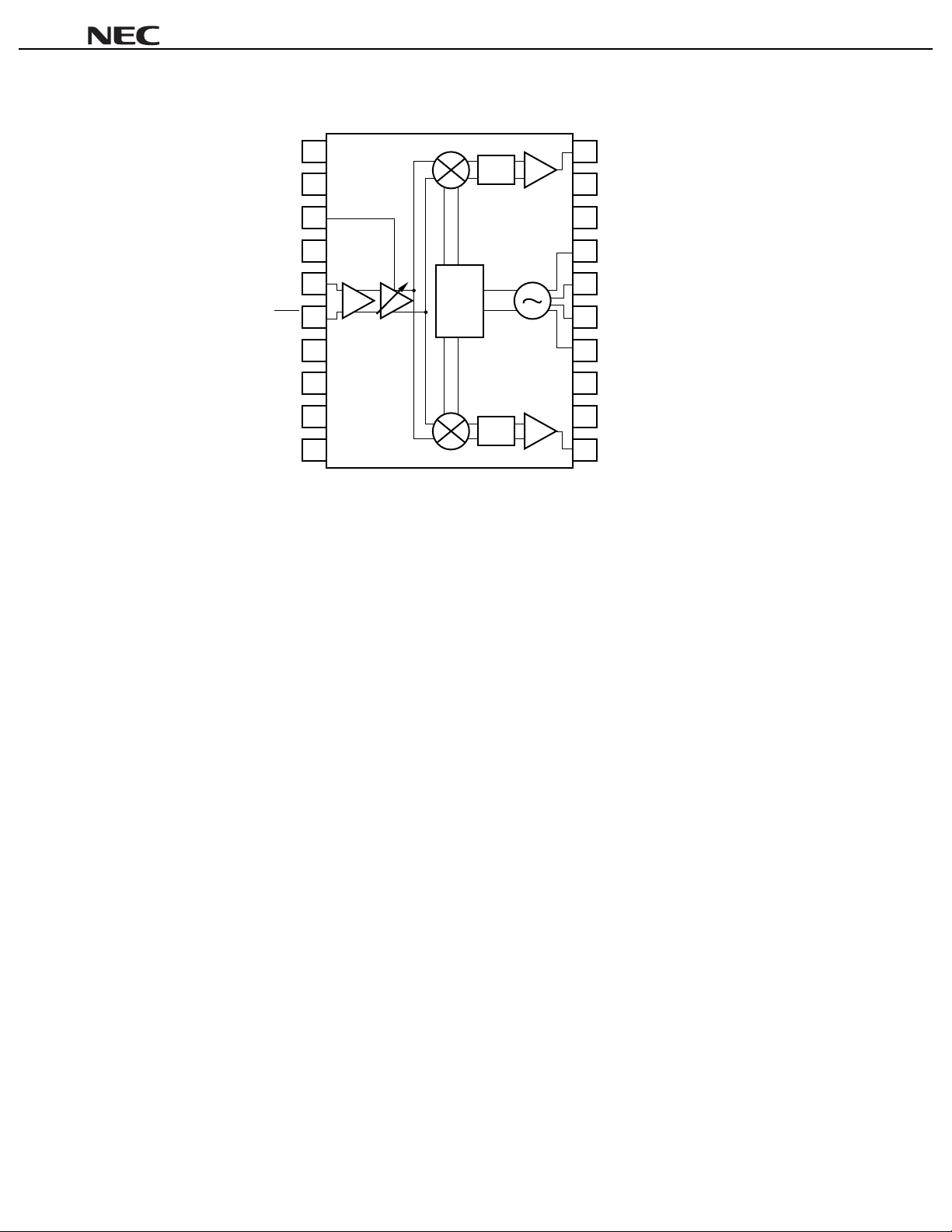
INTERNAL BLOCK DIAGRAM AND PIN CONFIGURATION (Top View)
µµµµ
PC3205GR
V
CC
(I)
GND (I)
AGC
V
GND (IF)
IF IN
IF IN
GND (IF)
CC
(IF)
V
GND (Q)
V
CC
(Q)
1
2
3
4
5
6
7
8
9
10
IF
Amplifier
AGC
Amplifier
MIXER
90 deg
phase
shifter
0°
90°
LPF
LPF
OSC
20
19
18
17
16
15
14
13
12
11
I OUT
GND (PS)
V
CC
(PS)
OSC-C1
OSC-B2
OSC-B1
OSC-C2
GND (PS)
GND (PS)
Q OUT
2
Data Sheet P13541EJ3V0DS00

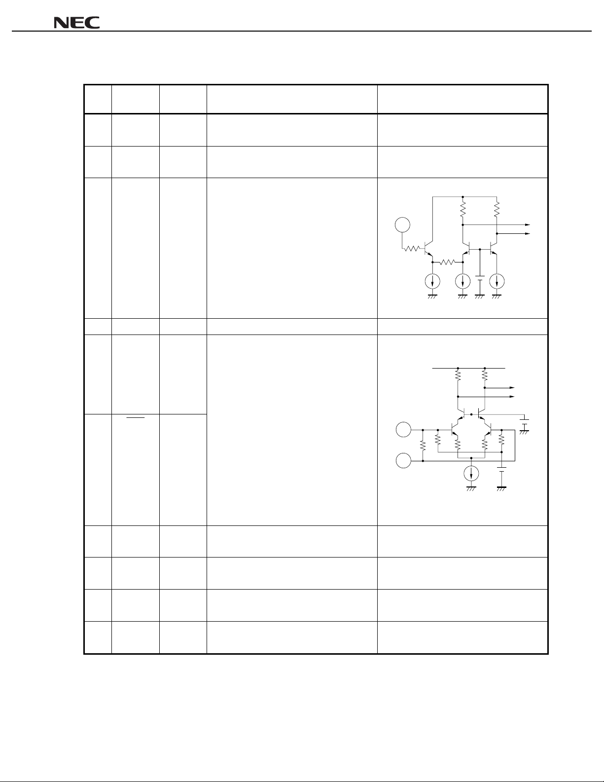
PIN FUNCTIONS
µµµµ
PC3205GR
Pin
No.
Pin
Name
1VCC(I) 5.0 Supply voltage pin.
2 GND(I) 0.0 Ground pin.
3V
4 GND(IF) 0.0 Ground pin.
5IF IN 2.7
AGC
Pin Voltage
TYP. (V)
0 to 5 Gain control pin.
AGC
V
= 0 V: Full gain
AGC
V
= 5 V: Full reduction
IF input pins. In case of single input, 5 pin or
6 pin should be grounded through capacitor.
Function and Explanation Equivalent Circuit
3
6IF IN 2.7
7 GND(IF) 0.0 Ground pin.
8VCC(IF) 5.0 Supply voltage pin.
9 GND (Q) 0.0 Ground pin.
10 VCC (Q) 5.0 Supply voltage pin.
5
6
Data Sheet P13541EJ3V0DS00
3

µµµµ
PC3205GR
Pin
No.
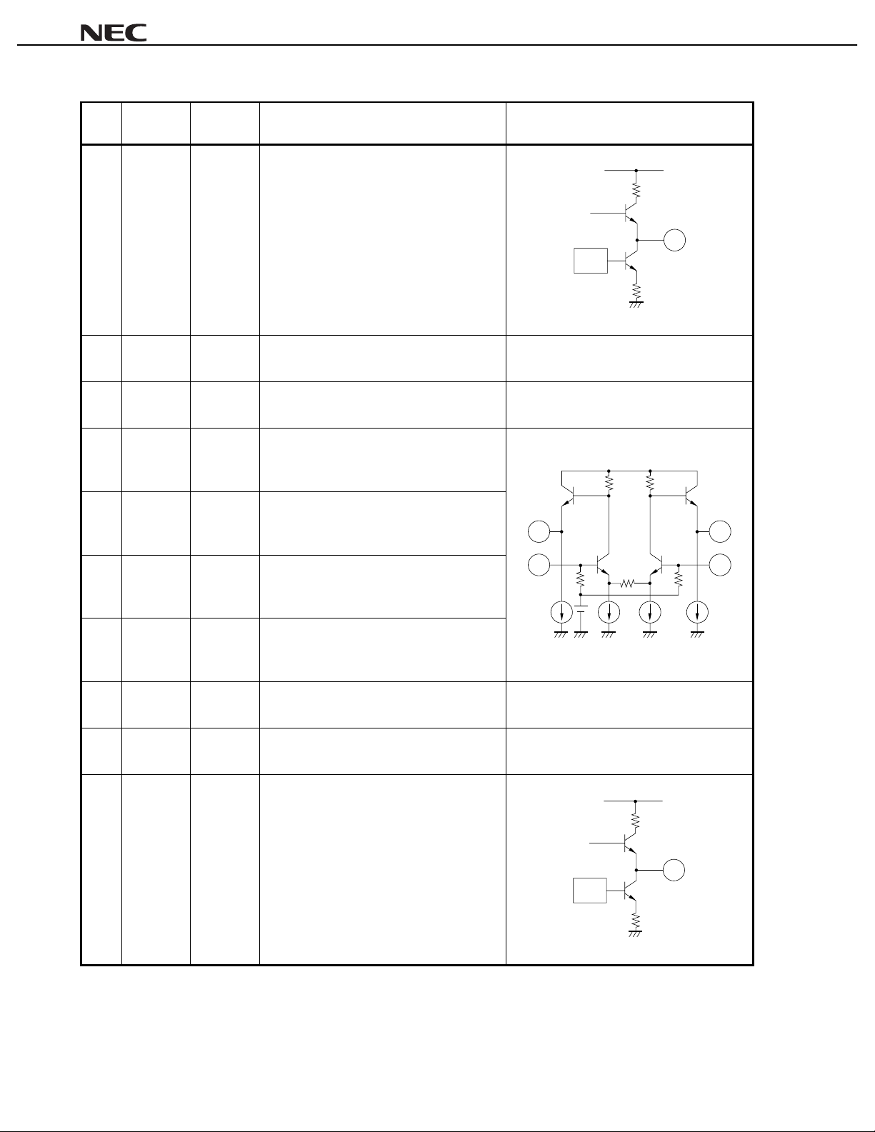
11 Q OUT 2.6 Q-signal output pi n.
12 GND(PS) 0.0 Ground pin.
13 GND(PS) 0.0 Ground pin.
14 OSC-C2 3.4 Connected capacitor bet ween 14 pi n and 15
15 OSC-B1 3. 0 Connect ed SAW resonator through
Pin
Name
Pin Voltage
TYP. (V)
Function and Explanation Equivalent Circuit
pin to oscillate with active f eedback loop.
capacitor.
14
11
REG
17
16 OSC-B2 3. 0 Connect ed SAW resonator through
capacitor.
17 OSC-C1 3.4 Connected capacitor bet ween 16 pi n and 17
pin to oscillate with active f eedback loop.
18 VCC(PS) 5.0 Supply voltage pin.
19 GND(PS) 0.0 Ground pin.
20 I OUT 2.6 I-signal output pin.
16
15
20
REG
4
Data Sheet P13541EJ3V0DS00

ABSOLUTE MAXIMUM RATINGS (TA = +25°C unless otherwise specified)
Parameter Symbol Test Condition Rating Unit
µµµµ
PC3205GR
Supply Voltage V
Power Dissipation P
Operating Ambient Temperature
Storage Temperature T
Mounted on 50 mm × 50 mm × 1.6 mm double epoxy glass board.
Note
CC
TA = +85°C
D
A
T
stg
Note
RECOMMENDED OPERATING RANGE
Parameter Symbol Test Condition MIN. TYP. MAX. Unit
T
AGC
CC
A
IF
V
out
= 1 V
P-P
Supply Voltage V
Operating Ambient Temperature
IF Input Level Range P
Gain Control Voltage Range V
ELECTRICAL CHARACTERISTICS (TA = +25°C, VCC = 5 V, Zin = 50
Parameter Symbol Test Conditions MIN. TYP. MAX. Unit
Circuit Current I
IF Input Frequency f
IQ Output Frequency f
Conversion Gain 1 Gcv1 fIF = 490 MHz, f
Conversion Gain 2 Gcv2
Conversion Gain 3 Gcv3 fIF = 490 MHz, f
AGC Gain Control Range GCR fIF = 490 MHz, f
IQ Phase Balance
IQ Amplitude Balance
Output Voltage V
Maximum Output Voltage Voclip
CC
No input signal 48 65 78 mA
OSC
fIF > f
IF
IQ
Gcv (@fIQ = 10 MHz) ± 1 dB, Vout = 1 V
PIF = –45 to –25 dBm
AGC
V
= 0 to 0.5 V
IF
= 490 MHz, f
f
AGC
V
= 4.5 V to V
AGC
V
= 0.5 to 4.5 V
fIF = 490 MHz, f
φ
∆
PIF = –45 to –25 dBm
VfIF = 490 MHz, f
∆
PIF = –45 to –25 dBm
fIQ = 0.3 to 30 MHz, PIF = –45 to –25 dBm
out
AGC
= 0 to 0.5 V, PIF = –45 to –25 dBm
V
OSC
= 479.5 MHz
OSC
= 479.5 MHz, V
OSC
= 479.5 MHz
CC
OSC
= 479.5 MHz
OSC
= 479.5 MHz, V
OSC
= 479.5 MHz, V
6.0 V
433 mW
–40 to +85 °C
–55 to +150 °C
4.5 5.0 5.5 V
–25 +25 +85 °C
–45 – –25 dBm
0.0 – V
out
, Z
= 1 k
ΩΩΩΩ
)
ΩΩΩΩ
Note
P-P
Note
Note
AGC
= 2 V
Note
Note
Note
out
P-P
= 1 V
Note
P-P
= 1 V
out
Note
Note
Note
CC
V
440 – 520 MHz
0.3 – 30 MHz
49 53 – dB
–44–dB
– – 10 dB
39 – – dB
–2 0 +2 deg
–0.5 0 +0.5 dB
–1.0–V
1.8 – – V
P-P
P-P
By measurement circuit 1
Note
Data Sheet P13541EJ3V0DS00
5

µµµµ
PC3205GR
STANDARD CHARACTERISTICS (TA = +25 °C, VCC = 5 V, Zin = 50
Parameter Symbol Test Conditions Reference Value Unit
OSC
= 479.5 MHz, fIQ = 10 MHz, V
Noise Figure (DSB) NF
Third Order Intermodulation
Distortion
LO to IF Isolation Iso(LO-IF)
LO to IQ Isolation Iso(LO-IQ) f = 480 MHz
I to Q Isolation Iso(I-Q)
IF Input Impedance Zin(IF) fIF = 480 MHz 138-j45
IF Input Return Loss RL(IF) fIF = 480 MHz 6 dB
IQ Output Impedance ZO(IQ) fIQ = 0.3 to 30 MHz 25
Notes 1.
By measurement circuit 2
By measurement circuit 1
2.
IM
f
3
fIF1 = 489 MHz, fIF2 = 490 MHz, f
out
V
= 0.708 V
f = 480 MHz, 15 pin or 16 pin to 5 pin
15 pin or 16 pin to 11 pin or 20 pin
f = 10 MHz, 11 pin to 20 pin
P-P
/tone
out
, Z
ΩΩΩΩ
AGC
= 0.5 V
OSC
= 479.5 MHz
= 1 k
)
ΩΩΩΩ
Note 1
Note 2
Note 2
Note 2
Note 2
12.5 dB
56 dBc
50 dB
30 dB
30 dB
Ω
Ω
6
Data Sheet P13541EJ3V0DS00
 Loading...