NEC UPC3202GR-E1, UPC3202GR Datasheet

DATA SHEET
BIPOLAR ANALOG INTEGRATED CI RCUIT
µµµµ
PC3202GR
FREQUENCY DOWN CONVERTER FOR
VHF to UHF BAND TV/VCR TUNER
DESCRIPTION
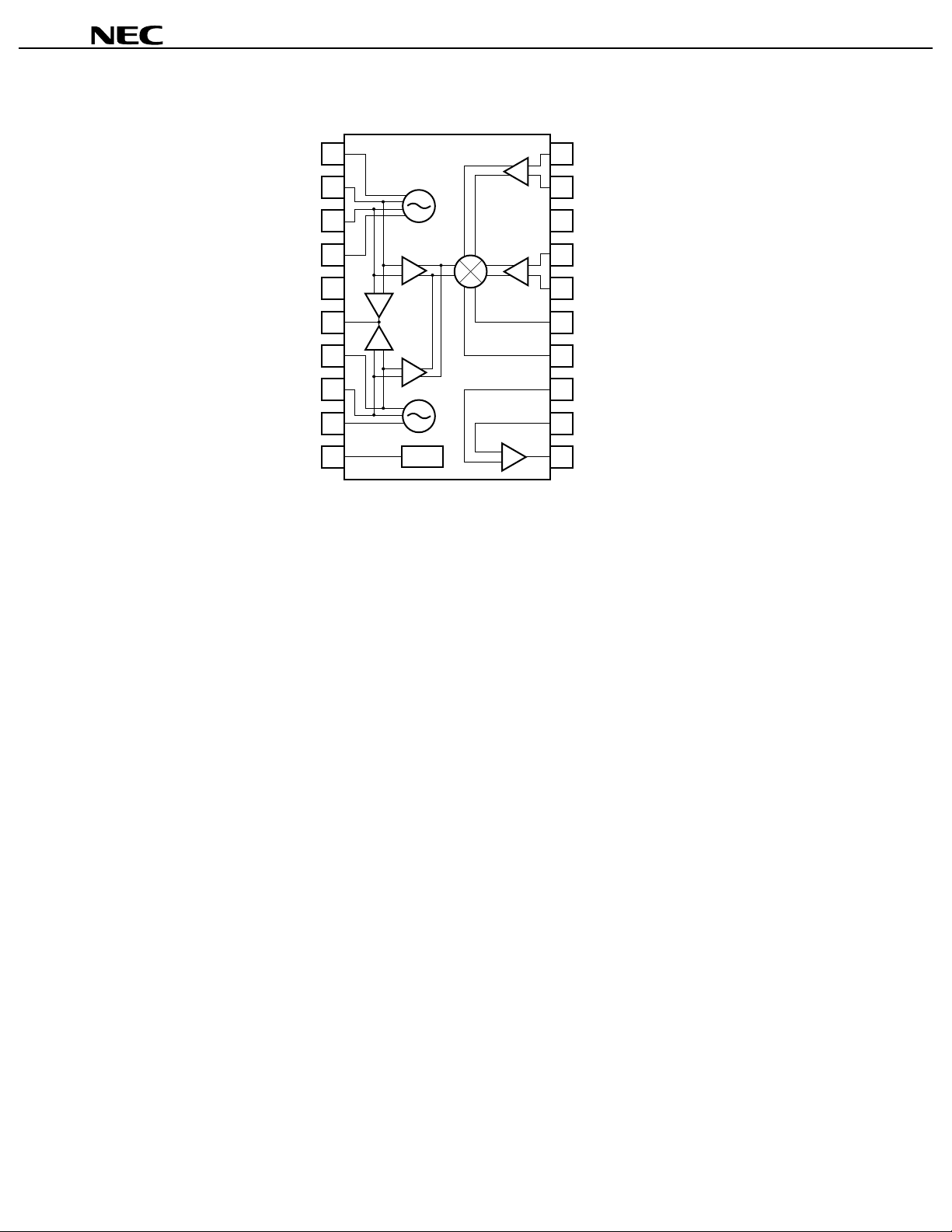
The µPC3202GR is Silicon monolithic IC designed for TV/VCR tuner applications. This IC consists of a double
balanced mixer (DBM), local oscillator, preamplifier for precscaler operation, IF amplifier, regulator, and so on. This
one-chip IC covers a wide frequency band from VHF to UHF bands. This IC is packaged in 20-pin SSOP (Shrink
Small Outline Package) suitable for surface mounting.
FEATURES
• VHF to UHF band operation.
• Low power dissipation Vcc = 5 V, Icc = 41 mA
• Packaged in 20-pin SSOP suitable for surface mounting
TYP.
ORDERING INFORMATION
Part Number Package Package Style
µ
PC3202GR-E1 20-pin plastic SSOP
(225 mil)
For evaluation sample order, please contact your local NEC office. (Part number for sample order: µPC3202GR)
Embossed tape 12 mm wide. 2. 5 k/REEL
Pin 1 indicates pull-out di rection of tape
The information in this document is subject to change without notice. Before using this document, please
confirm that this is the latest version.
Not all devices/types available in every country. Please check with local NEC representative for
availability and additional information.
Document No. P12151EJ3V0DS00 (3rd edition)
Date Published October 1999 N CP(K)
Printed in Japan
Caution electro-static sensitive device
The mark shows major revised points.
©
1996, 1999

INTERNAL BLOCK DIAGRAM AND PIN CONFIGURATION (Top View)
µµµµ
PC3202GR
UOSC C1
UOSC B2
UOSC B1
UOSC C2, UB
GND
OSC OUT
VOSC B1
VOSC B2
VOSC C1
V
120
2
3
4
5
6
7
8
9
CC
10 11
U OSC
V OSC
REG
URF IN
19
URF IN (bypass)
18
GND
17
VRF IN
16
VRF IN (bypass)
15
MIX OUT
14
MIX OUT
13
IF IN
12
IF IN
IF OUT
2
Data Sheet P12151EJ3V0DS00

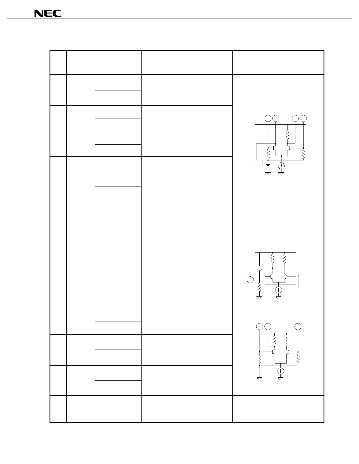
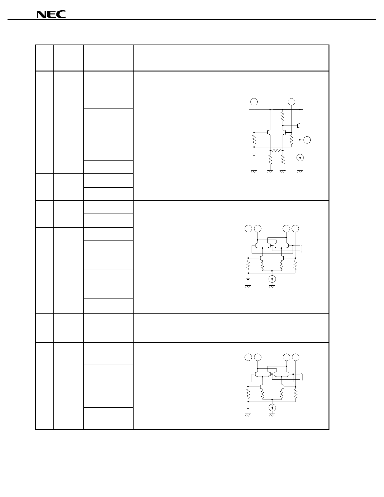
PIN EXPLANATION
µµµµ
PC3202GR
Pin
No.
Symbol
collector
(Tr.1)
base
(Tr.2)
base
(Tr.1)
collector
(Tr.2)
and UB
Pin Voltage TYP.
above: VHF mode
below: UHF mode
5.001UOSC
3.60
0.02UOSC
1.90
0.03UOSC
1.90
0.04UOSC
5.00
0.05GND
Function and Explanation Equivalent Circuit
Collector pin of UHF oscillator.
Assemble LC resonator with 2 pin
through 1 pF capacitor to oscillate with
active feedback loop.
Base pin of UHF oscillator with balance
amplifier. Connected to LC res onator
through 360 pF feedback capacitor.
Base pin of UHF oscillator with balance
amplifier. Connected to LC res onator
through 360 pF feedback capacitor.
Collector pin of UHF oscillator with
balance amplifier. Grounded through
6 pF capacitor.
Double balanced oscillator with transistor
1 and transistor 2.
And this pin is swit ch for VHF or UHF.
VHF operation = GND
UHF operation = 5.0 V
GND pin for VHF and UHF oscillator
REG
2
4 1 3
output
base
(Tr.1)
base
(Tr.2)
collector
(Tr.2)
0.0
2.706OSC
2.35
1.957VOSC
0.0
1.958VOSC
0.0
3.609VOSC
5.00
5.0010 Vcc
VHF and UHF oscillator signal output pin.
In case of F/S tuner application,
connected PLL symthesizer IC’s input
pin.
Base pin of VHF oscillator.
Grounded through 10 pF capacitor.
Base pin of VHF oscillator.
Assemble LC resonator with 10 pi n to
oscillate with active feedbac k loop.
Collector pin of VHF oscillator.
Connected to LC resonator through 3
pF feedback capacitor.
Power supply pin.
6
from
OSC
798
5.00
Data Sheet P12151EJ3V0DS00
3

µµµµ
PC3202GR
Pin
No.
Symbol
output
(bypass)
Pin Voltage TYP.
above: VHF mode
below: UHF mode
2.5511 IF
2.55
2.0012 IF IN
2.00
2.0013 IF IN
2.00
5.0014 MIX OUT
5.00
5.0015 MIX OUT
5.00
2.8016 VRF IN
2.85
Function and Explanation Equivalent Circuit
IF signal output pin for V HF and UHF
operation.
13
IF signal input pins. Connected to Mixer
output pins through 1000 pF capacit ors.
VHF and UHF MIX output pins.
These pins should be equipped with tank
circuit to adjust i ntermediate frequency
Bypass pin for VHF MIX i nput .
Grounded through 1000 pF capacitor.
12
11
16151417
from
VHF
OSC
(bypass)
2.8017 VRF IN
2.85
0.018 GND
0.0
2.8519 URF IN
2.80
2.8520 URF IN
2.80
VHF RF signal input pin.
GND pin of MIX, IF ampli fier and
regulator.
Bypass pin for UHF MIX i nput .
Grounded through 1000 pF capacitor.
UHF RF signal input pin.
16151419
from
UHF
OSC
4
Data Sheet P12151EJ3V0DS00

µµµµ
PC3202GR
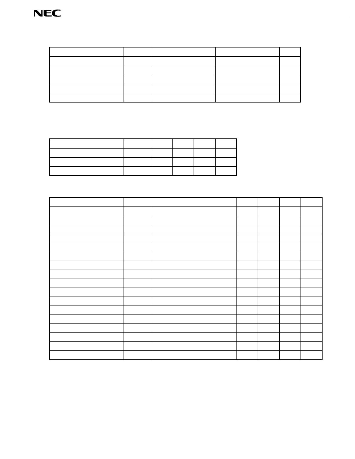
ABSOLUTE MAXIMUM RATINGS (TA = 25°C unless otherwise specified
)
Parameter Symbol Condition Ratings Unit
Supply voltage 1 V
CC
6.0 V
Supply voltage 2 UB 6.0 V
TA = 80°C
Power dissipation P
Operation temperature range T
Storage temperature range T
Mounted on 50 × 50 × 1.6 mm double cupper epoxy glass board.
*1
D
A
stg
*1
466 mW
–20 to +80 °C
–55 to +150 °C
RECOMMENDED OPERATING RANGE
Parameter Symbol MIN. TYP. MAX. Unit
Supply voltage 1 V
Supply voltage 2 UB 4.5 5.0 5.5 V
Operation temperature range T
ELECTRICAL CHARACTERISTICS (TA = 25°C, VCC = 5 V, f
Parameter Symbol Test Conditions MIN. TYP. MAX. Unit
Circuit Current 1 ICC1
Circuit Current 2 Icc2
Conversion Gain 1 CG1
Conversion Gain 2 CG2
Conversion Gain 3 CG3
Conversion Gain 4 CG4
Conversion Gain 5 CG5
Noise Figure 1 NF1
Noise Figure 2 NF2
Noise Figure 3 NF3
Noise Figure 4 NF4
Noise Figure 5 NF5
Maximum Output Power 1 P
Maximum Output Power 2 P
Maximum Output Power 3 P
Maximum Output Power 4 P
Maximum Output Power 5 P
CC
A
O(SAT)
O(SAT)
O(SAT)
O(SAT)
O(SAT)
4.5 5.0 5.5 V
–20 +25 +80 °C
osc
@VHF, no input signal
@UHF, no input signal
RF
f
= 55 MHz, PRF = –30 dBm
RF
f
= 200 MHz, PRF = –30 dBm
RF
f
= 470 MHz, PRF = –30 dBm
RF
f
= 470 MHz, PRF = –30 dBm
RF
f
= 800 MHz, PRF = –30 dBm
RF
f
= 55 MHz
RF
f
= 200 MHz
RF
f
= 470 MHz
RF
f
= 470 MHz
RF
f
= 800 MHz
RF
f
1
2
3
4
5
= 55 MHz, PRF = 0 dBm
RF
f
= 200 MHz, PRF = 0 dBm
RF
f
= 470 MHz, PRF = 0 dBm
RF
f
= 470 MHz, PRF = 0 dBm
RF
f
= 800 MHz, PRF = 0 dBm
= fRF + 45 MHz, fIF = 45 MHz, P
*1
34.0 41.0 48.0 mA
*1
34.0 41.0 48.0 mA
*2
22.0 25.0 28.0 dB
*2
22.0 25.0 28.0 dB
*2
22.0 25.0 28.0 dB
*2
26.0 29.0 32.0 dB
*2
26.0 29.0 32.0 dB
*3
*3
*3
*3
*3
*2
*2
*2
*2
*2
−
−
−
−
−
4.0 6.0
4.0 6.0
4.0 6.0
4.0 6.0
4.0 6.0
10.5 13.0 dB
10.5 13.0 dB
10.5 13.0 dB
9.5 12.0 dB
10.0 13.0 dB
OSC
= –10 dBm)
−
−
−
−
−
dBm
dBm
dBm
dBm
dBm
By measurement circuit 1
*1
By measurement circuit 2
*2
By measurement circuit 3
*3
Data Sheet P12151EJ3V0DS00
5

STANDARD CHARACTERISTICS (Reference Values) (TA = 25°C, VCC = 5 V)
µµµµ
PC3202GR
Parameter Symbol Test Conditions
Third order intermodulation distort i on 1 IM31VHF, fRF1 = 470 MHz, fRF2 = 476 MHz,
OSC
Pin = –30 dBm each, f
OSC
= –10 dBm
P
= 515 MHz,
Third order intermodulation distort i on 2 IM32 UHF, fRF1 = 800 MHz, fRF2 = 806 MHz,
OSC
Pin = –30 dBm each, f
OSC
= –10 dBm
P
= 845 MHz,
1% cross-modulation dis tortion 1 CM1 VHF, fRF = 470 MHz, fundes = 476 MHz,
OSC
= 515 MHz, PRF = –40 dBm,
f
OSC
= –10 dBm, AM100 kHz,
P
30% modulation, DES/CM = 46 dB c
1% cross-modulation dis tortion 2 CM2 UHF, fRF = 800 MHz, fundes = 806 MHz,
OSC
= 845 MHz, PRF = –40 dBm,
f
OSC
= –10 dBm, AM100 kHz,
P
30% modulation, DES/CM = 46 dB c
By measurement circuit 4
*1
*1
*1
*1
*1
Value for
Reference
55 dBc
46 dBc
96 dB
88 dB
Unit
µ
µ
6
Data Sheet P12151EJ3V0DS00
 Loading...