NEC UPC305G2, UPC305C Datasheet

DATA SHEET
BIPOLAR ANALOG INTEGRATED CI RCUT
µµµµ
PC305
POSITIVE VOLTAGE STABILIZED POWER SUPPLY
DESCRIPTION
The µPC305 is a high-performance stabilized power supply that can supply a constant voltage in a wide
temperature range even if the input voltage or load voltage fluctuates, by integrating a high-gain error amplifier and a
temperature-compensating constant-voltage diode on a single chip.
FEATURES PIN CONFIGURATION (Top View)
Wide output voltage variable range Vo: 4.5 to 30 V, V
•
Excellent load stability 0.02%
•
Good ripple rejection ratio 0.003%/V
•
DIF
: 3 to 30 V
Current limiter
Current output
Input
GND
µ
PC305C, 305G2
1
2
3
4
8
7
6
5
Output
Compensation
Error detection
Reference voltage
ORDERING INFORMATION
Part Number Package
PC305C 8-pin plastic DIP (7.62 mm (300))
µ
PC305G2 8-pin plastic SOP (5.72 mm (225))
µ
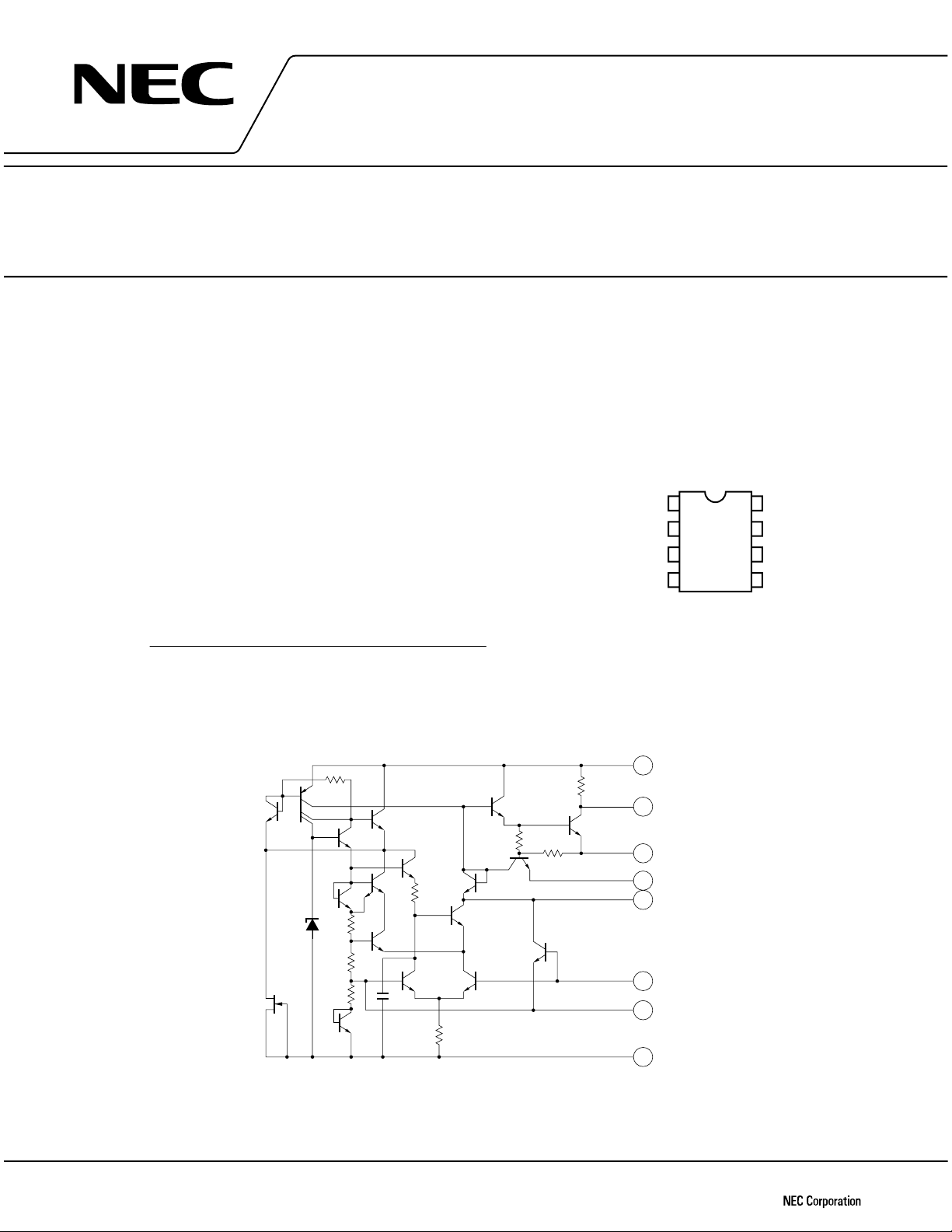
EQUIVALENT CIRCUIT
R
7
2.8 kΩ
Q
Q
11
12
Q
13
Q
10
Q
9
Q
7
6
Q
8
R
4
1
D
3 kΩ
R
3
6.8 k
Ω
R
3 kΩ
2
Q
1
Q
18
R
4.4 kΩ
Q
Q
4
2
Q
1
C
5 pF
R
5
2.2 kΩ
1.86 kΩ
6
Q
5
Q
3
Input
R
9
R
1.32 kΩ
600 Ω
Q
15
Q
14
R
8
Q
16
Q
17
3
10
Current output
2
Current limiter
1
Output
8
Compensation
7
Error detection
6
Reference voltage
5
GND
4
The information in this document is subject to change without notice. Before using this document, please
confirm that this is the latest version.
Not all devices/types available in every country. Please check with local NEC representative for
availability and additional information.
Document No. G10633EJ3V0DS00 (3rd edition)
Date Published December 1999 N CP(K)
Printed in Japan
©
1999

µµµµ
PC305
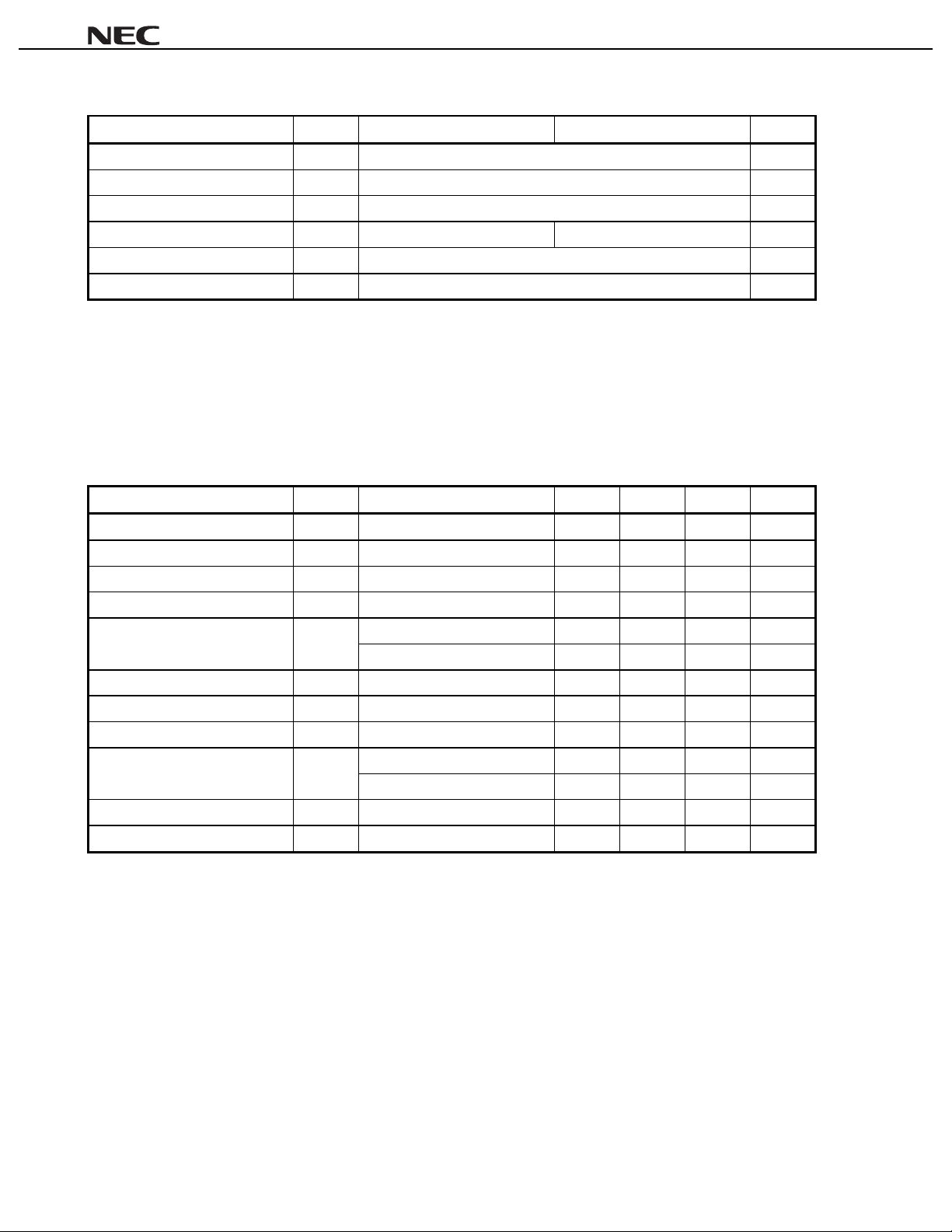
ABSOLUTE MAXIMUM RATINGS (Unless otherwise specified, TA = 25
Parameter Symbol
Input Voltage V
Input − Output Voltage Difference V
Maximum Output Current I
Total Loss P
Operating Temperature T
Storage Temperature T
A
Notes 1.
Where T
Where TA > +25°C, perform derating at TJ MAX. 125°C, −4.4 mW/°C.
2.
> +55°C, perform derating at TJ MAX. 125°C, −5 mW/°C.
IN
DIF
O
T
A
stg
PC305C
µ
350
Note 1
0.3 to +40 V
−
40 V
50 mA
0 to +70
55 to +125
−
C)
°°°°
PC305G2 Unit
µ
Note 2
440
mW
C
°
C
°
Caution If any of the parameters exceeds the absolute maximum ratings, even momentarily, the quality of
the product may be impaired. The absolute maximum ratings are values that may physically
damage the product(s). Be sure to use the product(s) within the ratings.
ELECTRICAL SPECIFICATIONS (Unless otherwise specified, TA = 25
Parameter Symbol Condition MIN. TYP. MAX. Unit
Input Voltage Range V
Output Voltage Range V
Input − Output Voltage Difference V
Load Stability REG
Ripple Rejection Ratio REJ C
Temperature Stability 0°C ≤ TA ≤ 70°C0.31.0%
Reference Voltage V
Long-time Stability 0.1 %
Supply Current under No Load I
IN
OUT
DIF
L
0 ≤ IO ≤ 12 mA, RSC = 18
IN
REF
N
CC
OUT
VIN – V
VIN – V
≤ 5 V 0.025 0.06 %/VInput Stability REG
OUT
> 5 V 0.015 0.03 %/V
REF
= 10 µF, f = 120 Hz 0.003 %/V
10 Hz ≤ f ≤ 10 kHz, C
REF
C
= 0.1 µF 0.002 %
VIN = 40 V 1.0 2.0 mA
REF
Ω
= 0 µF 0.005 %Output Noise Voltage V
C)
°°°°
8.0 40 V
4.5 30 V
3.0 30 V
0.02 0.05 %
1.65 1.8 1.90 V
Remark
2
SC
: Current-limiting resistor
R
REF
C
: Bypass capacitor of reference voltage pin
Data Sheet G10633EJ3V0DS00

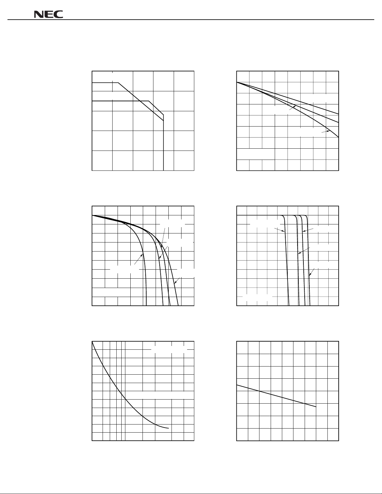
STANDARD CHARACTERISTIC CURVES
= 25
(Unless otherwise specified, T
A
C. Reference values)
°°°°
µµµµ
PC305
500
400
300
[mW]
T
200
Total Loss P
100
0
0
−0.02
−0.04
PT vs TA Characteristics
µ
PC305G
µ
PC305C
Operating Temperature TA [°C]
Load Stability (2)
TA = 0°C
TA = 25°C
Load Stability (1)
0
−0.01
−0.02
−0.03
Output Voltage Fluctuation (%)
−0.04
100
RSC = 0 Ω
0100806040200 51015
80
60
TA = 0°C
Output Current I
Current-limiting Characteristics
TA = +70°C
A
= +70°C
T
TA = −20°C
O
(mA)
TA = 0°C
TA = 25°C
−0.06
Outout Voltage Fluctuation (%)
−0.08
−0.1
0 102030
3.0
2.8
2.6
Resistance (kΩ)
2
2.4
R
2.2
2.0
51020
TA = +70°C
RSC = 13 Ω
Output Current I
Resistance for Setting Output Voltage
Output Voltage (V)
O
(mA)
R1//R2 = 2 kΩ
R1 = 1110×V
R
2
TA = −20°C
Output Voltage Drop Ratio (%)
40
OUT
(Ω)
Pickup Voltage Across Pins <1> and <8> (V)
50 0806020
TA = −20°C
40
20
RSC = 13 Ω
0
050
0.63.2
0.5
0.4
0.3
0.2
10 20 30 40
Output Current I
Current-limiting Pickup Voltage
Operating Temperature T
40
O
(mA)
A
(°C)
Data Sheet G10633EJ3V0DS00
3
 Loading...