


DATA SHEET
BIPOLAR ANALOG INTEGRATED CIRCUIT
µ
PC2533
AM TUNER FOR ELECTRONIC TUNING CAR RADIOS
The µPC2533 is an IC developed as an AM tuner for car stereos and car radios.
It employs an up-conversion type double super-heterodyne configuration (IF1 = 10.71 MHz, IF2 = 450 kHz).
The internal configuration consists of the MIX1 block (MIX1, OSC1, Buff1), MIX2 block (MIX2, OSC2, Buff2), IF
amplifier, detection circuit, AGC circuit, signal meter circuit, SD (station detector) circuit, and Lo/DX (short range/long
range) circuit.
Features
• Possible to select stations using only one varactor diode with narrow variable capacitance range
• Tracking adjustment unnecessary
• Coil switching between LW (long wave) and MW (middle wave) unnecessary
• Less sensitivity deviation due to tracking error
• High S/N: 60 dB
• Signal meter output with good linearity
• Signal meter output voltage inclination setting possible by external resistor.
• Can be used with IF (intermediate frequency) counter turning system or high/low tuning system.
Type Number
µ
PC2533GS-01 Set by pin No. 7 Set by pin No. 9 Depends on SD SD sensitivity of IF counter
µ
PC2533GS-02 Set by pin No. 7 Set by pin No. 9 Tilt of the signal meter
•LO/DX function on-chip
• Since IFT (intermediate frequency transformer) turn ratio is free from limitation for matching of ceramic filter
impedance, it is easy to design MIX gain with IFT.
IF Counter Output High/Low Output
SD Sensitivity Setting
Signal Meter Voltage
Inclination Setting
sensitivity setting system and high/low system
can be set independently.
voltage can be set without
regard to SD sensitivity.
Remarks
The information in this document is subject to change without notice.
Document No. S11989EJ4V0DS00 (4th edition)
Date Published August 1998 N CP(K)
Printed in Japan
The mark shows major revised points.
©
1993
Ordering Information
Part Number Package
µ
PC2533GS-01 36-pin plastic shrink SOP (300 mil)
µ
PC2533GS-02 36-pin plastic shrink SOP (300 mil)
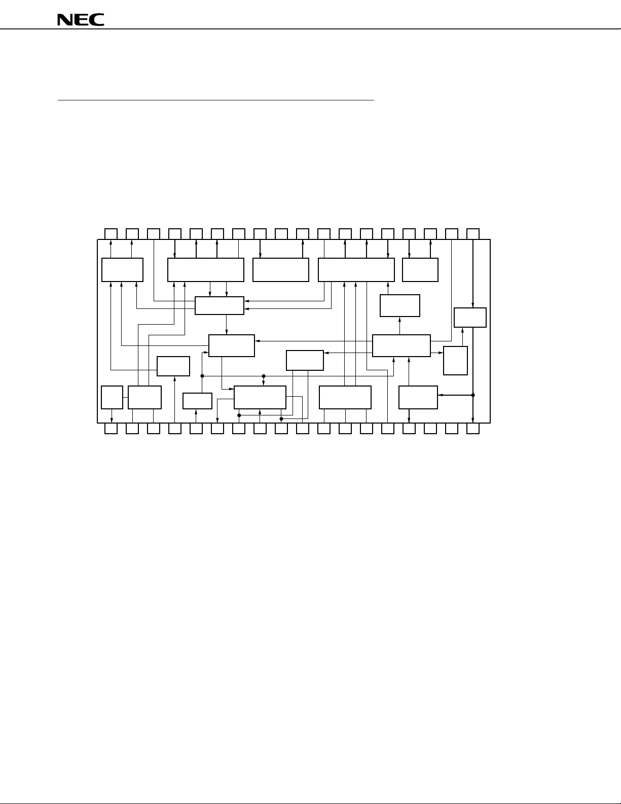
Block Diagram
RF AGC1
RF AGC2
RF AGC T.C.
MIX1IN
MIX1OUT
MIX1OUT
MIX1BYP
Buff1IN
35 34 33 32 31 30 29 28 27 26 25 24 23 22 21 20 1936
GND
Buff1OUT
MIX2BYP
MIX2OUT
MIX2OUT
MIX2IN
Buff2IN
Buff2OUT
IF AGC T.C.
IF2IN
µ
PC2533
RF AGC
driver
L
OSC
OSC 1
Buff
2345671 8 9101112131415161718
1
ref
ALC
V
OSC1 Buff
MIX 1 Buff 1 MIX 2 Buff 2
RF AGC
detector
AGC
comparator
O
/DX
Station
detector
SD ACOUT
SD ACadj [SDadj]
SD IFIN
/DX
O
L
SEEK
SEEK
Remarks 1. Bold lines indicate flow of audio signal.
2.µPC2533GS-02 pin names are in parentheses. Pins not in parentheses are used in both the
µ
PC2533GS-01 and µPC2533GS-02.
Signal
meter
OSC 2 Detector
OSC2 (B)
SD DCOUT
SD DCadj [SMOUT]
OSC2 (E)
MIX 2
AGC
Time constant
selector switch
2
ref
V
MIX2AGC T.C.
(AF)
O
V
GND
IF
amplifier
IF
AGC
CC
V
IF2OUT
2
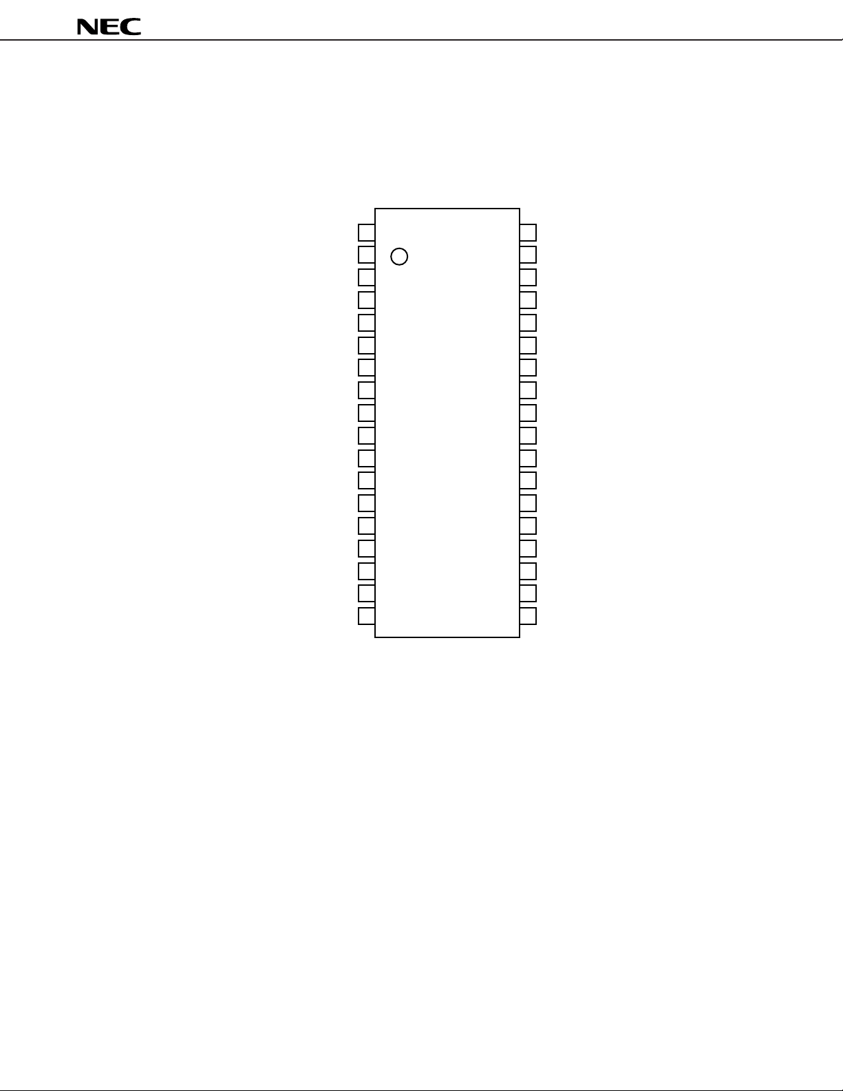
Pin Configuration (Top View)
36-pin plastic shrink SOP (300 mil)
•µPC2533GS-01
•µPC2533GS-02
µ
PC2533
OSC1 Buff
ALC
V
ref
L
O
/DX
SEEK
SD ACOUT
SD ACadj [SDadj]
SD IFIN
SD DCadj [SMOUT]
SD DCOUT
OSC2 (B)
OSC2 (E)
V
ref
MIX2AGC T.C.
O
(AF)
V
GND
V
IF2OUT
1
2
3
1
4
5
6
7
8
9
10
11
12
13
2
14
15
16
17
CC
18
RF AGC1
36
35
RF AGC2
34
RF AGC T.C.
33
MIX1IN
32
MIX1OUT
31
MIX1OUT
30
MIX1BYP
29
Buff1IN
28
GND
27
Buff1OUT
26
MIX2BYP
25
MIX2OUT
24
MIX2OUT
23
MIX2IN
Buff2IN
22
21
Buff2OUT
20
IF AGC T.C.
19
IF2IN
RemarkµPC2533GS-02 pin names are in parentheses. Pins not in parentheses are used in both the
µ
PC2533GS-01 and µPC2533GS-02.
3
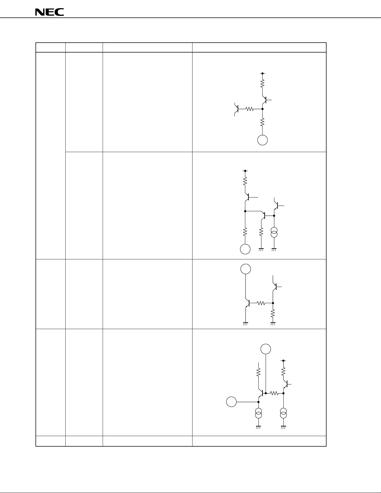
1. Pin Description
V
ref
5 kΩ
5
60 kΩ
Names and symbols in parentheses indicate pin names for µPC2533GS-02. Names and symbols not in
parentheses are pin names used in both the µPC2533GS-01 and µPC2533GS-02.
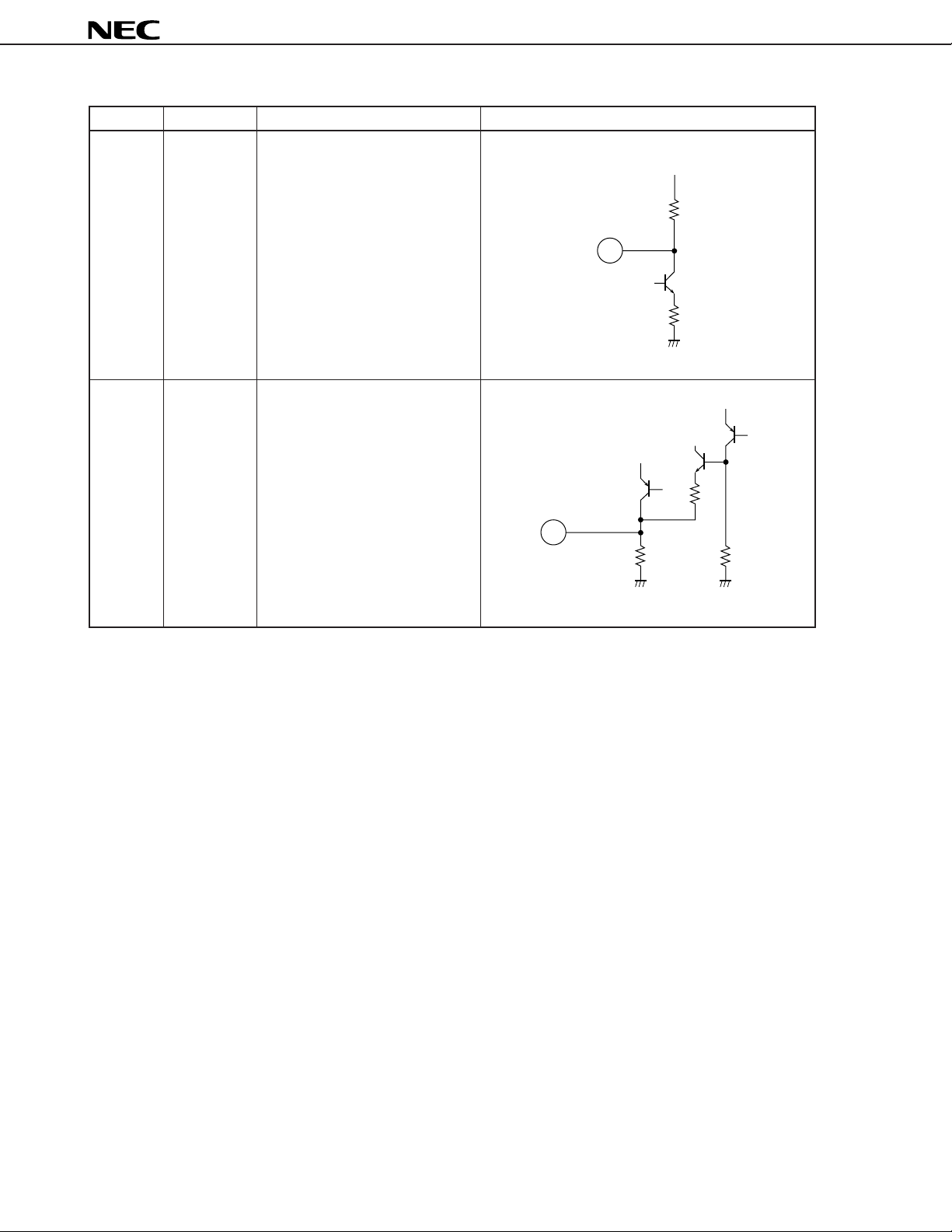
Pin No. Symbol Name Equivalent Circuit
1 OSC1 Buff OSC1 Buff output
2 ALC OSC1 ALC
ZO = 30 Ω ±20 %
V
CC
1
VCC
2
µ
PC2533
(1/7)
3Vref1 Reference voltage Reference voltage (5.3 V)
4LO/DX LO/DX control
4
5 SEEK Seek request
4
V
CC
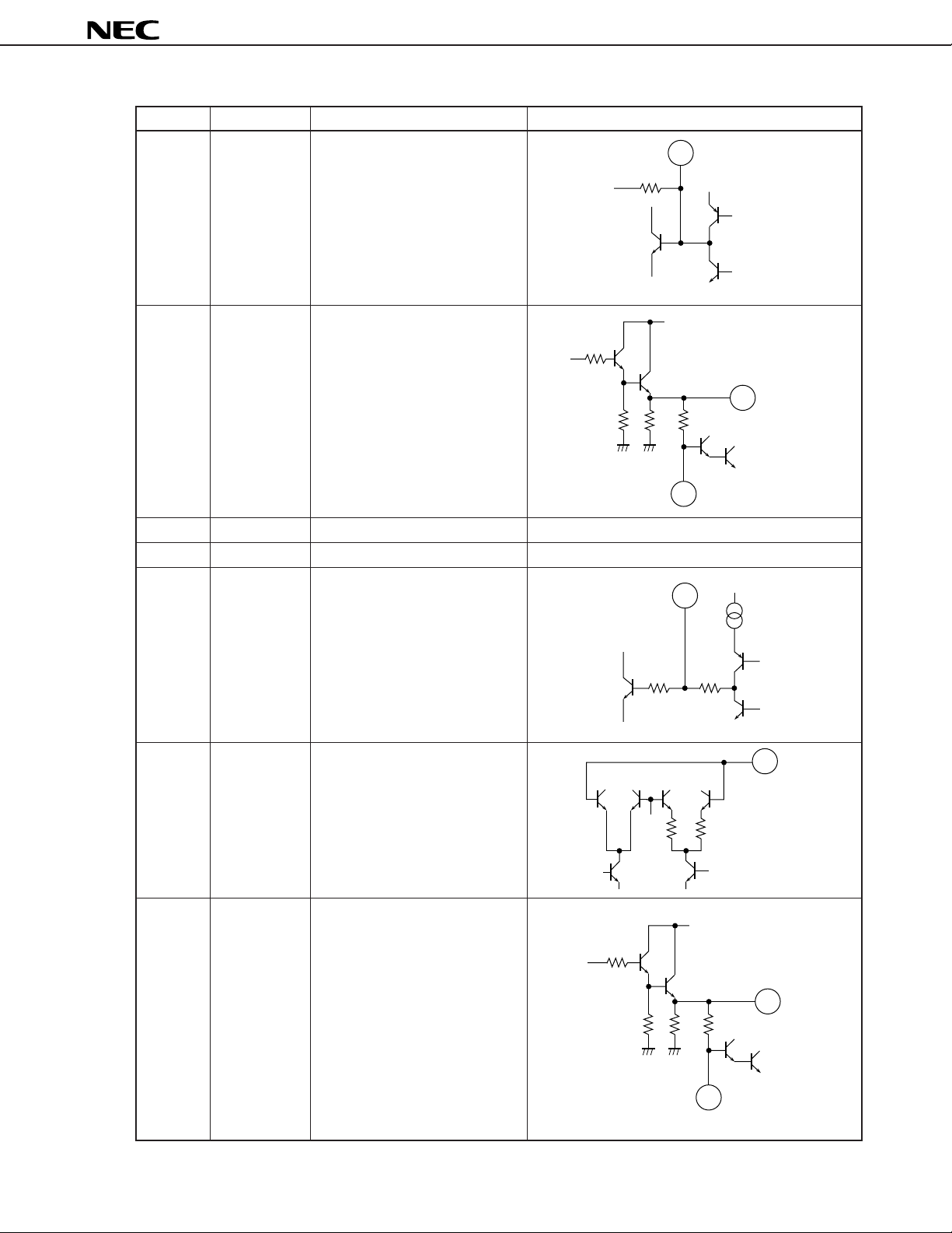
Pin No. Symbol Name Equivalent Circuit
V
CC
7
5 kΩ
( PC2533GS-01)
µ
6 SD ACOUT SD AC output
O
= 20.5 kΩ ±20 %
R
500 Ω
6
20 kΩ
7 SD ACadj SD AC sensitivity setting
(and signal meter ouput)
µ
PC2533
(2/7)
[SDadj] [SD AC sensitivity and SD DC
sensitivity setting]
8 SD IFIN SD IF input
µ
( PC2533GS-02)
V
CC
5 kΩ
7
Vref
60 kΩ
500 Ω
5.2 V
8
5
Pin No. Symbol Name Equivalent Circuit
V
CC
9
5 kΩ
( PC2533GS-01)
µ
9 SD DCadj SD DC sensitivity setting
(and signal meter output)
µ
PC2533
(3/7)
[SMOUT] [Signal meter output]
10 SD DCOUT SD DC output (Active high)
11 OSC2 (B) OSC2 (base)
12 OSC2 (E) OSC2 (emitter)
µ
( PC2533GS-02)
V
5 kΩ
9
10
Z
IN
V
ref
CC
5.2 V
= 5 kΩ ±20 %
11
V
CC
6
ZO = 240 Ω ±20 %
12
13 Vref2 Reference voltage Reference voltage (6.0 V)
Pin No. Symbol Name Equivalent Circuit
18
14 MIX2AGC T.C. MIX2 AGC smoothing
ref
V
14
T
= 1 kΩ ±20 %
R
R
T
µ
PC2533
(4/7)
15 VO(AF) Audio output
16 GND Ground GND (low frequency)
17 VCC Power supply voltage VCC
18 IF2OUT IF amplifier output
19 IF2IN IF amplifier input
V
CC
ZO = 300 Ω ±20 %
20
15
19
20 IF AGC T.C. IF AGC input
VCC
15
T
R
20
RT = 100 kΩ ±20 %
7
Pin No. Symbol Name Equivalent Circuit
21
Z
O
= 2 kΩ ±20 %
22
V
ref
ZIN = 30 kΩ ±20 %
21 Buff2OUT 2nd IF burffer output
22 Buff2IN 2nd IF buffer input
23 MIX2IN MIX2 input
µ
PC2533
(5/7)
24 MIX2OUT MIX2 output
25 MIX2OUT MIX2 output
26 MIX2BYP MIX2 bypass
27 Buff1OUT 1st IF buffer output
23
23
Z
IN
25 24
26
Z
IN
= 330 Ω ±20 %
26
= 330 Ω ±20 %
8
27
Z
O
= 330 Ω ±20 %
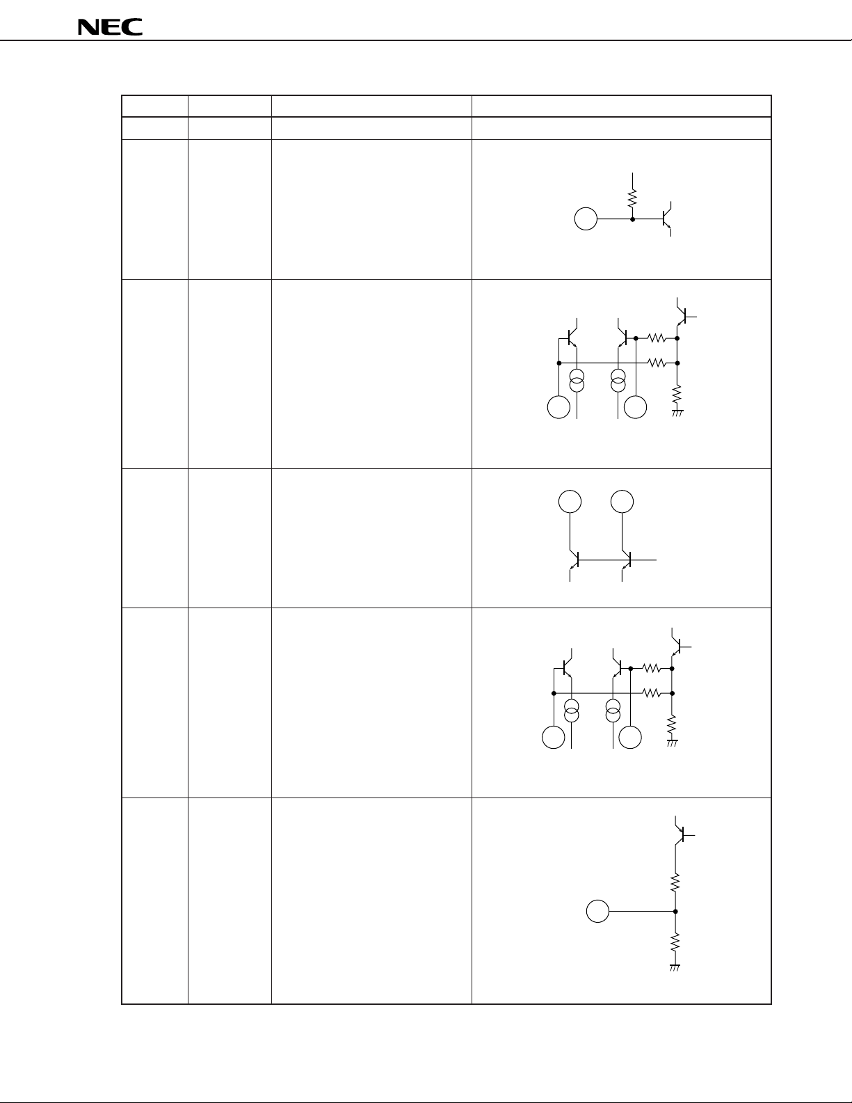
Pin No. Symbol Name Equivalent Circuit
ZIN = 1.2 kΩ ±20 %
33 30
34
Z
O
= 12 kΩ ±20 %
28 GND Ground GND (high frequency)
29 Buff1IN 1st IF buffer input
V
ref
29
Z
IN = 15 kΩ ±20 %
30 MIX1BYP MIX1 bypass
33 30
µ
PC2533
(6/7)
31 MIX1OUT MIX1 output
32 MIX1OUT MIX1 output
33 MIX1IN MIX1 input
34 RF AGC T.C. RF AGC smoothing
ZIN = 1.2 kΩ ±20 %
31 32
V
ref
9
Pin No. Symbol Name Equivalent Circuit
35 RF AGC2 RF AGC output (cascade base)
Vref
O = 11 kΩ ±20 %
Z
35
36 RF AGC1 RF AGC output (PIN diode)
µ
PC2533
(7/7)
36
O
= 22 kΩ ±20 %
Z
10
2. Operation of Each Block
2.1 FR Amplifier Circuit Block
VCC
R1
L3
R2
L1
Q1
Q2
L2
C1
+
C9
C8
Fig. 2-1 RF Ampliier Circuit
LPF
L4 L5
C3 C4 C5
C6
33
30
C7
35
36
MIX1
From MIX2
RF AGC L
O/DX
µ
PC2533
Note
C2
34
+
4
Note LO : 3 V or higher
DX : 1 V or lower
In the AM band, the capacitance of a car radio antenna depends on its length, diameter, cable length, etc. Therefore,
µ
J-FET is used in the
PC2533 to raise RF input impedance.
Since the µPC2533 raises the first IF (intermediate frequency) to 10.71 MHz, there is no need for a tuning circuit
between the RF amplifier circuit and MIX1. Instead, it employs an LPF (about 6 MHz) consisting of L4, L5 and C3
to C5 between the RF amplifier circuit and MIX1 in order to cut image frequency (21.4 MHz or higher). Because this
allows a wide-band RF amplifier circuit to be configured without using a tuning circuit, frequency sensitivity deviation
can be minimized to a high degree.
The AGC circuit consists of RF AGC1 by the PIN diode connected to the FET gate and RF AGC2 by the cascade
transistor Q1. Use a low-noise transistor even with low current for the cascade transistor Q1 (if a high-noise one is
used, the S/N ratio deteriorates).
Remark Set bias voltage for cascade transistor Q1 to V
C > VB.
11

2.2 MIX1 Block
Fig. 2-2 MIX1 Block
µ
PC2533
From
LPF
V
T
+
23 32
Q101
R11
OSC1
Q105
Q109
1
R107
28
33
30
T1
31
Q106 Q107
To 10.7 MHz
CC
V
17
Q104
Q103Q102
Q108
R109
R110
R108
To RF AGC circuit (Fig. 2-4)
29 27
Bias circuit
BPF
R112
Buff1
Note
R111
Note Output impedance and input impedance of Buff1 are 330 Ω and 15 kΩ, respectively.
MIX1 (Q101 to Q108) is a DBM (double balanced mixer).
MIX1 output is supplied to 10.7 MHz ceramic filter via Buff1 (output impedance: 330 Ω) for impedance matching.
The local oscillation signal is applied to the bases of Q101 to Q104, and the RF signal to the base of Q105. MIX1
(Q101 to 108) multiplies the local oscillation signal by RF signal, and converts to the resonance frequency of IFT T1
for output.
µ
The local oscillation signal is output from pin 1 via Q109 (OSC Buff). It has an amplitude of 110 dB
V and can
be directly input to CMOS LSI for use by the PLL synthesizer.
The RF signal applied to the base of Q105 is also input to the detector of the RF AGC circuit.
12

2.3 MIX2 Block
From 10.7 MHz BPF
µ
PC2533
Fig. 2-3 MIX2 Block
V
CC
28 23 17 24 25 14 13 12 11 22 21
Note
+
Xtal
To IF amplifier
R211
Bias
circuit
R210
R209
To RF AGC circuit (Fig. 2-4)
Current control
circuit
Q201
Q202 Q203
Q205
Q206
R207 R208
Q204
Q207
R212
Buff2
Note
Q203
OSC2
Q208
From IF AGC (Fig. 2-6)
Note Output impedance and input impedance of Buff2 are 2 kΩ and 30 kΩ, respectively.
MIX2 (Q201 to Q208) is a DBM with a configuration similar to that of MIX1.
The major difference from the MIX1 is that MIX2 is equipped with a current control circuit for output and is controlled
by the AGC.
Input impedance of MIX2 is 330 Ω to match the 10.7 MHz ceramic filter. Output impedance of Buff2 is 2 kΩ to
match the 450 kHz ceramic filter.
IF signal input from pin 23 is also input to the detector of the RF AGC. The RF AGC is detected by both MIX1 and
MIX2 blocks.
The Buff1 and Buff2 ensure impedance matching between MIX1 and MIX2 outputs and each ceramic filter. As
a result, IFT design is not restricted by the need to match ceramic filter impedance. For turn ratio, etc., only conversion
gain need be taken input account, so it is easy to design.
13

2.4 RF AGC Block
Fig. 2-4 RF AGC Block
R412
µ
PC2533
Bias circuit
R402
To RF amplifier
circuit (Fig. 2-1)
Q402
Q401
Q403
R403
R405
Q405
Time
constant
switchover
Q404
R404
R406
3536 34
Q406
D401
Q407 Q408
Detection
and
addition
R409
R410
R408
+
circuit
AMP.
AMP.
+
–
+
–
From MIX2
(Fig. 2-3)
From MIX1
(Fig. 2-2)
The configuration of the RF AGC is shown in Fig. 2-4. After being detected by the RF AGC detector and added,
the input signal from MIX1 and MIX2 is smoothed by external capacitor of pin 34, and its DC voltage controls the RF
AGC.
RF AGC output controls the PIN diode from pin 36 and controls base voltage of cascade transistor which determines
DS from pin 35. In addition, by detecting sudden fluctuation of pin 34 voltage and switching over time constants,
FET V
RF AGC response convergence when the electric field suddenly changes is improved.
Operation start time of the RF AGC can be delayed slightly by connecting a resistor parallel to the external capacitor
of pin 34.
14

2.5 IF Amplifier Block and Detection Block
Fig. 2-5 IF Amplifier and Detection Block
µ
PC2533
From 450kHz BPF To SD circuit
R19
+
C19
19 18
IF amp
T3
17
–
R303
Q301
Q302
15
R304
Bias circuit
R301 R302
+
V
CC
Audio
output
From IF AGC circuit
(Fig. 2-6)
To IF AGC circuit
(Fig. 2-6)
In the IF amplifier block, DC feedback is carried to pin 19 via an external low pass filter (composed of T3 and C19)
from pin 18, an output pin. The DC electric potential of pin 18 is designed to be fixed approximately equal to the (+)
side input of the IF amplifier. The value of R19 is the input impedance, so impedance matching to 450 kHz ceramic
filter is possible.
The output signal current of the IF amplifier is converted to signal voltage by being resonated by T3 and input to
the detection circuit after frequency selection.
Emitter follower detection by Q302 is adopted for the detection circuit block.
15

2.6 IF AGC Block
Fig. 2-6 IF AGC Block (for µPC2533GS-01)
µ
PC2533
V
CC
Bias circuit
To SD circuit
(Fig. 2-7)
From SD circuit
(Fig. 2-7)
To MIX2 (Fig. 2-3) To IF amp. (Fig. 2-5)
Signal meter circuit
Note
R501
R502
5 kΩ
5 kΩ
7 209
Q503
Q501
D501
Q502
Q504
D502
From detection circuit
(Fig. 2-5)
Time
constant
switchover
Note In the case of PC2533GS-02,
+
the part enclosed by the
dotted line is illustrated as
shown below.
R501
5 kΩ
µ
Voltage
limiter
R502
5 kΩ
IF AGC block configuration is shown in Fig. 2-6. The signal detected from pin 15 is smoothed by the capacitor
of pin 20, and its DC voltage controls the IF AGC.
The IF AGC controls the IF amplifier and MIX2. In the operation sequence, it first controls the gain of the IF amplifier,
then controls the gain of MIX2.
The signal meter circuit output (current output) is in proportion to the DC voltage smoothed by pin 20, and converted
to voltage by the external resistor of pin 7 or 9. Therefore, output voltage value and gain can be set by the value of
the external resistor.
Note
Note For relation between the external resistor and the signal meter, refer to Signal meter output voltage
(adjustment by resistor between pin 9 and GND) in section 4. Characteristic Curves.
16

2.7 Station Detector Circuit Block
(
)
Fig. 2-7 Station Detector Circuit Block
µ
PC2533
ON/OFF
SD AC output
450kHz IF input
(from T3)
Bias circuit
From signal meter
circuit (Fig. 2-6)
+
1.0 V
+
Detection comparator 2
–
–
SD output
Active high
Detection comparator 1
1.0 V
10 5 6 8
–
+
To time constant
switchover circuit
(Fig. 2-6)
From DTS (request)
The configration station detector (SD) circuit block is shown in Fig. 2-7.
The SD circuit stops scanning or seeking when a broadcast wave is received when auto scanning or seek tuning.
µ
Since the
PC2533 has two outputs (DC high/low signal (open collector) and AC IF signal (f = 450 kHz)), it can be
used according to DTS (digital tuning system) type. Input the SD request signal from DTS to pin 5.
µ
The SD sensitivity setting methods of the
PC2533GS-01 and µPC2533GS-02 differ.
With the µPC2533GS-01, SD sensitivities in the IF counter output system and in the high/low output system are
set by external resistor between pin 7 and GND and by external resistor between pin 9 and GND.
µ
With the
PC2533GS-02, SD sensitivities in both the IF counter output system and high/low output system are set
by external resistor between pin 7 and GND (refer to Fig. 2-6).
Bias circuit
Table 2-1 SD Sensitivity Setting Examples
Value of Resistor between Pin 9 or Pin 7 and GND SD Sensitivity (AC, DC)
51 kΩ 27 dBµV
24 kΩ 29 dBµV
10 kΩ 33 dBµV
17

µ
PC2533
The reference voltage of the µPC2533-01 and µPC2533-02 detection comparator has been internally fixed at
1.0 V.
Under the influence of R501 (5 kΩ) and R502 (5 kΩ) of the siganl meter circuit (Fig. 2-6), signal meter output voltage
and detection comparator input voltage do not perfectly coincide. For SD sensitivity setting, refer to the following
formula.
Detection comparator input voltage =
Signal meter output voltage × (1 +
Value of resistor between pin 7 and GND
Remark Because DC output is open-collector type (Active high), connect pull-up resistor to pin 10 to use.
R501
)
18

µ
PC2533
3. Electical Characteristics
Absolute Maximum Ratings (TA = 25 °C)
Item Symbol Rating Unit
Power supply voltage VCC 10 V
Power dissipation PD 600 mW
Operating ambient temperature TA –40 to +85 °C
Storage temperature Tstg –55 to +125 °C
Caution Exposure to Absolute Maximum Ratings for extended periods may affect device reliability;
exceeding the ratings could cause permanent damage. The parameters apply independently.
The device should be operated within the limits specified under DC and AC Characteristics.
Recommended Operating Conditions (T
Item Symbol Conditions MIN. TYP. MAX. Unit
Power supply voltage VCC 7.5 8.0 8.5 V
Input voltage VIN 132 dBµV
A = 25 ˚C)
Electrical Characteristics
(Unless specified, TA = 25 °C, VCC = 8 V, fIN = 999 kHz, fMOD = 400 Hz, AMMOD = 30 %, RSD1 (resistor between pin
7 and GND) = R
Circuit current ICC No input (excluding FET) – 45 55 mA
Detection output VO VIN = 74 dBµV 150 180 210 mVrms
Signal-to-noise ratio S/N VIN = 74 dBµV5360–dB
Total harmonic distortion 1 THD1 VIN = 74 dBµV – 0.3 1.0 %
Total harmonic distortion 2 THD2 VIN = 74 dBµV, AMMOD = 80 % – 0.7 1.0 %
Total harmonic distortion 3 THD3 VIN = 130 dBµV, AMMOD = 80 % – 0.7 1.5 %
Signal meter output voltage 1 VS1 No input – 0 0.2 V
Signal meter output voltage 2 VS2 VIN = 30 dBµV 0.5 1.5 2.5 V
Signal meter output voltage 3
Local buffer output 1 VOSC 1-pin load: 20 pF or less 106 110 114 dBµV
SD2 (resistor between pin 9 and GND) = 24 kΩ, 15-pin measurement load = 100 kΩ)
Item Symbol Conditions MIN. TYP. MAX. Unit
Note
VS3 VIN = 74 dBµV 4.8 5.5 6.7 V
(4.3) (5.0) (5.5)
Note Specifications in parentheses for signal meter output voltage 3 are for µPC2533GS-02. Values of other items
µ
are the same for
PC2533GS-01 and µPC2533GS-02.
19

µ
Reference Characteristics
Item Symbol Conditions MIN. TYP. MAX. Unit
Maximum sensitivity MS VIN making VO –10 dB, where – 13 – dBµV
VO = 0 dB at VIN = 74 dBµV
S/D sensitivity (AC) SS(AC) V IN making SEEK, SD AC – 29 – dBµV
OUT level 101 dBµV or more
S/D sensitivity (DC) SS(DC) VIN making SEEK, SD AC – 29 – dBµV
OUT voltage 4.8 V or more
S/D output time T-SD Delay time from the time when 0 5 25 ms
changing SEEK VIN = 0 → 40
dBµV to the time when pin 10
voltage becomes 4.8 V or more
Vo stabilization time T-VO VIN = 60 → 100 dBµV, 60 160 260 ms
VO = ±3 dB
Tweet TW VIN = 74 dBµV, 2IF – 60 – dB
2nd local buffer negative ZOSC2 Maximum value of a series 400 – – Ω
impedance resistor with which the crystal
can oscillate
Usable sensitivity US VIN making S/N = 20 dB – 25 – dBµV
PC2533
20

4. Characteristic Curves
Input/Output Characteristics (1)
µ
PC2533
MS (VO =
–10 dB)
0
7
–10
6
US (at S/N=20 dB)
–20
5
(dB), Noise (dB)
–30
O
4
–40
3
–50
2
–60
1
Total harmonic level V
–70
0
Total harmonic distortion THD (%), Signal meter voltage (V)
0 10 20 30 40 50 60 70 80 90 100 110 120 130
MS = 14 dB VµUS = 25 dB V
THD 80 %
Input/Output Characteristics (2)
( PC2533GS-01)
µ
Signal meter voltage
( PC2533GS-02)
µ
THD 30 %
µ
Signal input level (dB V)
Noise
µ
V
O
CC
V
f
IN
= 999 kHz
f
MOD
MOD
AM
R
SD1
=8 V
= 400 Hz
= 30 %
= R
SD2
= 24 kΩ
0
7
6
5
MS (VO =
–10 dB)
–10
–20
(dB), Noise (dB)
O
–30
US (at S/N=20 dB)
( PC2533GS-01)
µ
Signal meter voltage
( PC2533GS-02)
µ
4
–40
3
–50
2
–60
1
Detection output level V
–70
0
Total harmonic distortion THD (%), Signal meter voltage (V)
0 10 20 30 40 50 60 70 80 90 100 110 120 130
MS = 12.5 dB V
US = 28 dB V
µ
THD 80 %
THD 30 %
µ
Signal input level (dB V)
V
O
Noise
µ
VCC = 8 V
IN
= 216 kHz
f
f
MOD
= 400 Hz
AM
MOD
= 30 %
R
SD1
= R
SD2
= 24 kΩ
21

Input/Output Characteristics (3) (FET Load: 255 Ω) (Reference Only)
V
0
–10
O
µ
PC2533
–20
(dB), Noise (dB)
–30
O
–40
–50
–60
Detection output level V
–70
0 10 20 30 40 50 60 70 80 90 100 110 120 130
0
(dB)
N
–10
–20
(dB), Noise V
O
–30
Noise
Signal input level (dB V)
Input/Output Characteristics (4)
29 dB
VCC = 8 V
IN
= 999 kHz
f
f
MOD
= 400 Hz
AM
MOD
= 30 %
R
SD1
= R
SD2
= 24 kΩ
µ
V
O
V
O
VCC = 8 V
f
IN
= 999 kHz
f
MOD
= 400 Hz
AM
MOD
= 30 %
R
SD1
= R
SD2
= 24 kΩ
–40
–50
–60
Detection output level V
–70
010203040506070 8090100 120110 130
LO/DX low
L
O
/DX high
Signal input level (dB V)
µ
V
N
V
N
22

Cross-Modulation Characteristics (40 kHz Detuning)
µ
PC2533
0
–10
VCC = 8 V
(dB)
O
Detection output level V
Desired: f = 999 kHz
Interference: f = 1039 kHz
–20
–30
Desired:
V = 40 dB V
–40
45 dB V
60 dB V
–50
80 dB V
–60
50 60 70 80 90 100 110 120 130 140
µ
µ
µ
µ
µ
45 dB V
µ
40 dB V
Desired: 400 Hz 30% modulation; interference: non-modulation
Desired: non-modulation; interference: 400 Hz 30% modulation
Desired: non-modulation; interference: non-modulation
Interference signal input level (dB V)
Desired:
V = 100 dB V
80 dB V
60 dB V
100 dB V
µ
µ
µ
µ
µ
Cross-Modulation Characteristics (40 kHz Detuning, FET Load 255 Ω) (Reference Only)
Desired:
V = 100 dB V
80 dB V
60 dB V
µ
VCC = 8 V
Desired:
f = 999 kHz
Interference:
f = 1039 kHz
µ
µ
µ
–10
(dB)
O
–20
–30
–40
0
Desired:
V = 40 dB V
45 dB V
45 dB V
µ
40 dB V
µ
µ
µ
65 dB V
–50
Detection output level V
–60
0 60 70 80 90 100 110 120 130 140
80 dB V
50
µ
Desired: 400 Hz 30% modulation; interference: non-modulation
Desired: non-modulation; interference: 400 Hz 30% modulation
Desired: non-modulation; interference: non-modulation
Interference signal input level (dB V)
100 dB V
µ
µ
23

Cross-Modulation Characteristics (400 kHz Detuning)
µ
PC2533
0
VCC = 8 V
–10
Desired: f = 999 kHz
(dB)
O
Interference: f = 1399 kHz
–20
–30
Desired:
V = 40 dB V
µ
–40
µ
–50
Detection output level V
–60
60 dB V
µ
80 dB V
Desired: 400 Hz 30% modulation; interference: non-modulation
Desired: non-modulation; interference: 400 Hz 30% modulation
Desired: non-modulation; interference: non-modulation
60 70 80 90 100 110 120 130 140
50
Interference signal input level (dB V)
Power Supply Voltage Characteristics
0
Recommended
operating range
–10
50
µ
40
µ
30
20
10
µ
0
Maximum sensitivity MS (dB V), usable sensitivity
US (dB V), S/D sensitivity SS (dB V)
–20
–30
(dB), signal-to-noise ratio S/N (dB)
O
–40
–50
–60
Detection output level V
678910
Power supply voltage (V)
40 dB V
V
O
S3
V
SS
V
S2
S/N
µ
Desired:
V = 100 dB V
80 dB V
60 dB V
100 dB V
µ
6
5
4
3
US
2
MS
1
THD 80 %
THD 30 %
µ
µ
µ
µ
(V)
(V)
S2
S3
Signal meter output voltage 3 V
Total harmonic distortion THD (%),
Signal meter output voltage 2 V
24

Modulation Factor Characteristics
)
600
VCC = 8 V
f
IN
= 999 kHz
500
V
(mVrms)
400
O
µ
PC2533
O
3
2
1
Total harmonic distortion THD (%)
0
300
200
Detection output level V
100
0
20
THD
40 60 80 100
Modulation factor (%
Detuning Frequency Characteristics (Maximum Sensitivity), Signal Selectivity Characteristics
90
80
70
µ
60
50
40
30
Signal input level (dB V)
20
10
–10 –5 0 10 155–15
Detuning frequency (kHz)
25

Modulation Frequency Characteristics
)
µ
PC2533
0
–10
5
–20
4
3
2
1
Total harmonic distortion THD (%)
0
–30
–40
Detection output level (dB)
–50
–60
10
50 100 500 1k 5k 10k
Modulation frequency (Hz
VO
VCC = 8 V
THD
Signal Meter Output Voltage (Adjustment by Resistor between Pin 9 and GND)
7
51 kΩ
36 kΩ
6
5
VCC = 8 V
f
IN
= 999 kHz
MOD
= 30 %
AM
f
MOD
= 400 Hz
24 kΩ
(51 kΩ)
(24 kΩ)
20 kΩ
4
3
12 kΩ
2
Signal meter output voltage (V)
1
6.2 kΩ
(6.2 kΩ)
1 kΩ
(1 kΩ)
0 102030405060 8070 90 100
Signal input level (dB V)
µ
Remark Figures in parentheses indicate setting value (resistor between pin 9 and GND) for µPC2533GS-02. A
µ
circuit that restricts output current from pin 9 is mounted on
PC2533GS-02.
26

Receiving Frequency Characteristics
)
0
(LW band) (MW band)
–10
µ
PC2533
O
V
50
(dB),
O
–20
µ
40
µ
30
20
10
Maximum sensitivity MS (dB V),
usable sensitivity US (dB V)
0
–30
(LW band)
–40
–50
signal-to-noise ratio S/N (dB)
Detection output level V
(LW band)
–60
(LW band)
–70
0 0.2 0.4 0.6 0.8 1.0 1.2 1.4 1.6 1.8 2.0
(MW band)
(MW band)
(MW band)
US
S/N
MS
Receiving frequency (MHz
Temperature Characteristics (Signal Meter Voltage vs. Operating Ambient Temperature)
10
9
8
(V),
(V)
S2
S3
7
6
5
4
3
2
Signal meter output voltage 2 V
signal meter output voltage 3 V
1
0
–40 –20 0 20 40 60 80 100
V
S3
V
S2
Operating ambient temperature T
A
(°C)
27

µ
PC2533
Temperature Characteristics (Maximum Sensitivity, Usable sensitivity vs. Operating Ambient Temperature)
50
µ
40
30
20
10
Maximum sensitivity, Usable sensitivity (dB V)
0
–40 –20 0 20 40 60 80 100
Operating ambient temperature T
Usable
sensitivity
Maximum
sensitivity
A
(°C)
Temperature Characteristics (Detection Output Level, Signal-to-Noise Ratio vs. Operating Ambient Temperatue)
200
180
160
(mVrms)
O
140
V
O
0
–10
–20
–30
120
100
80
Detection output level V
60
40
–40 –20 0 20 40 60 80 100
Operating ambient temperature T
A
(°C)
S/N
–40
–50
–60
–70
–80
Signal-to-noise ratio S/N (dB)
28

Temperature Characteristics (THD vs. Operating Ambient Temperatue)
5
4
3
2
Input: 74 dB V
Modulation factor: 30 %
Input: 74 dB V
Modulation factor: 80 %
Input: 130 dB V
Modulation factor: 80 %
µ
µ
µ
µ
PC2533
1
Total harmonic distortion THD (%)
0
–40
THD1
–200 20406080100
Operating ambient temperature TA (°C)
THD2
THD3
29

PC2533
µ
2SC1844
+
3300 pF
µ
47 F
47 pF
510 Ω
0.022 F
0.047 F
µ
12 H
150 pF 100 pF
µ
L3
µ
12 H
µ
10 F
22 Ω
µ
T1 T2
0.022 F
50 Ω
0.022
µ
F
+
0.047 F
µ
µ
0.022 F
SFE10.7MHY-A CFWS450HT
µ
0.022 F
µ
26 25 24 23 22 21 20 1927282930313233343536
50 Ω
0.022
µ
F
4.7 F
+
2 kΩ
2.2 F
µ
µ
+
2SK1000
L2
L1
Dummy
antenna
65 pF
OSC1 Buff
OUT
30 Ω
SG IN
V
TUNE
15 pF
µ
0.01 F
100 kΩ
47 pF
KV1310 (TOKO, Inc.)
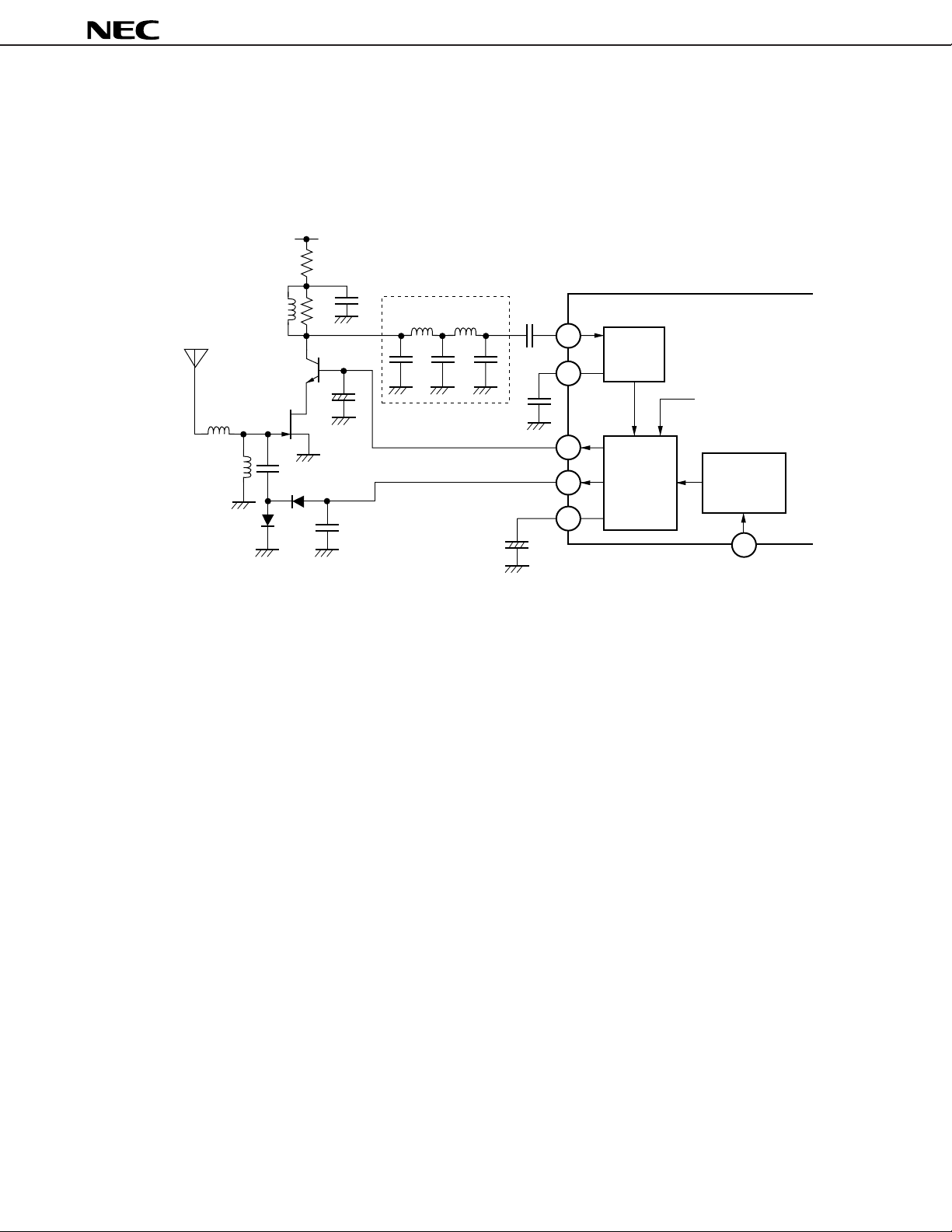
5. Measurement Circuit
RF AGC
driver
L
OSC
Buff
123456789101112131415161718
330 pF
OSC1
L4
µ
1 F
+
: 3 V or higher; DX: 1 V or lower)
O
(L
LO/DX
MIX1 Buff1 Buff2MIX2
RF AGC detection
AGC
comparator
O/DX
39
pF
0.01
µ
F
Station detector
RSD1
SD AC OUT
SEEK
SEEK (ON: 1.5 V or higher;
OFF: 0.3 V or lower)
0.01
F
µ
SDIN
[SDadj]
SD ACadj
Signal meter
SD2
R
[SMOUT]
SD DCadj
5 V
SD DC OUT
51
kΩ
OSC2
15 pF
47 pF
10.26 MHz
MIX2
AGC
Time constant
selector switch
+
10 F
µ
2.7 kΩ
µ
0.047 F
AUDIO OUT
Detector
µ
0.01 F
0.033 F
µ
47 F
+
µ
IF
AGC
V
CC
IF
amplifier
T3
(6)
(4)
(3)
(2)
(1)
PC2533GS-02.
µ
Remark Pin names in parentheses are those of
30

Coil Specifications (TOKO, Inc.)
Product No. Connection Diagram Prototype No. Specifications
L1 X119FNS-16314Z (1) - (3)
(3)
(4)
15T
µ
PC2533
(2)
(1)
L2 388DN-1043BS (4) - (6)
(3)
(2)
(1)
L3 247BR-0147Z (1) - (3)
(3)
(2)
(1)
L4 392AN - 1871Y (1) - (3) (1) - (2) (2) - (3)
(3)
(2)
(1)
T1 392AC-1883N (1) - (3) (1) - (2) (2) - (3)
(3)
(2)
(1)
T2 7PSYC-1779N (1) - (3) (1) - (2) (2) - (3)
(3)
(2)
(1)
T3 CX7YCS-8986N (1) - (3) (1) - (2) (2) - (3)
(3)
(2)
(1)
(6)
(4)
(6)
(4)
(6)
(4)
(6)
(4)
(6)
(4)
(6)
(4)
(6)
L = 4.7 µH
Qu > 60
1440T
L = 100 mH
Qu > 45
274T
L = 2 mH
Qu > 50
8T 4T 4T
L = 1.8 µH
Qu > 70
14T 7T 7T
(4) - (6)
C = 43 pF 3T
Qu > 50
fO = 10.7 MHz
152T 76T 76T
(4) - (6)
C = 180 pF 40T
Qu > 25
fO = 450 kHz
148T 43T 105T
(4) - (6)
C = 180 pF 30T
Qu > 40 ±20 %
fO = 450 kHz
• BPF SFE10.7 MHY-A (MURATA mfg. Co., Ltd.)
CFWS450HT (MURATA mfg. Co., Ltd.)
• RF FET 2SK1000 (NEC)
31

6. Package Drawing
36 PIN PLASTIC SSOP (300 mil)
118
A
F
G
µ
PC2533
1936
detail of lead end
R
H
I
J
C
DM
M
B
E
NOTE
Each lead centerline is located within 0.10 mm of
its true position (T.P.) at maximum material condition.
S
L
S
K
N
ITEM MILLIMETERS
A 15.3±0.24
B 0.97 MAX.
C 0.8 (T.P.)
D 0.37
E 0.125±0.075
F 1.675
G 1.55
H 7.7±0.3
I 5.6±0.15
J 1.05±0.2
K 0.22
L 0.6±0.2
M 0.10
N 0.10
R5°±5°
+0.08
−0.07
+0.125
−0.175
+0.08
−0.07
P36GM-80-300B-4
32

µ
PC2533
7. Recommended Soldering Conditions
When soldering this product, it is highly recommended to observe the conditions as shown below. If other soldering
processes are used, or if the soldering is performed under different conditions, please make sure to consult with our
sales offices.
For more details, refer to our document “SEMICONDUCTOR DEVICE MOUNTING TECHNOLOGY MANUAL”
(C10535E).
Surface mount device
µ
PC2533GS-01, 2533GS-02: 36-pin plastic shrink SOP (300 mil)
Process Conditions Symbol
Infrared ray reflow Peak temperature: 235 °C or below (Package surface temperature), IR35-00-2
Reflow time: 30 seconds or less (at 210 °C or higher),
Maximum number of reflow processes: 2 times.
VPS Peak temperature: 215 °C or below (Package surface temperature), VP15-00-2
Reflow time: 40 seconds or less (at 200 °C or higher),
Maximum number of reflow processes: 2 times.
Wave soldering Solder temperature: 260 °C or below, Flow time: 10 seconds or less, WS60-00-1
Maximum number of flow processes: 1 time,
Pre-heating temperature: 120 °C or below (Package surface temperature).
Partial heating method Pin temperature: 300 °C or below, –
Heat time: 3 seconds or less (Per each side of the device).
Caution Apply only one kind of soldering condition to a device, except for “partial heating method”, or
the device will be damaged by heat stress.
33

[MEMO]
µ
PC2533
34

[MEMO]
µ
PC2533
35

µ
PC2533
[MEMO]
The application circuits and their parameters are for reference only and are not intended for use in actual design-ins.
No part of this document may be copied or reproduced in any form or by any means without the prior written
consent of NEC Corporation. NEC Corporation assumes no responsibility for any errors which may appear in
this document.
NEC Corporation does not assume any liability for infringement of patents, copyrights or other intellectual property
rights of third parties by or arising from use of a device described herein or any other liability arising from use
of such device. No license, either express, implied or otherwise, is granted under any patents, copyrights or other
intellectual property rights of NEC Corporation or others.
While NEC Corporation has been making continuous effort to enhance the reliability of its semiconductor devices,
the possibility of defects cannot be eliminated entirely. To minimize risks of damage or injury to persons or
property arising from a defect in an NEC semiconductor device, customers must incorporate sufficient safety
measures in its design, such as redundancy, fire-containment, and anti-failure features.
NEC devices are classified into the following three quality grades:
"Standard", "Special", and "Specific". The Specific quality grade applies only to devices developed based on a
customer designated "quality assurance program" for a specific application. The recommended applications of
a device depend on its quality grade, as indicated below. Customers must check the quality grade of each device
before using it in a particular application.
Standard: Computers, office equipment, communications equipment, test and measurement equipment,
audio and visual equipment, home electronic appliances, machine tools, personal electronic
equipment and industrial robots
Special: Transportation equipment (automobiles, trains, ships, etc.), traffic control systems, anti-disaster
systems, anti-crime systems, safety equipment and medical equipment (not specifically designed
for life support)
Specific: Aircrafts, aerospace equipment, submersible repeaters, nuclear reactor control systems, life
support systems or medical equipment for life support, etc.
The quality grade of NEC devices is "Standard" unless otherwise specified in NEC's Data Sheets or Data Books.
If customers intend to use NEC devices for applications other than those specified for Standard quality grade,
they should contact an NEC sales representative in advance.
Anti-radioactive design is not implemented in this product.
34
M4 96.5
 Loading...