

Page 1
<R>
<R>
DATA SHEET
Solid State Relay
OCMOS FET
PS7360-1A,PS7360L-1A
6-PIN DIP, HIGH ISOLATION VOLTAGE
600 V BREAK DOWN VOLTAGE
NORMALLY OPEN TYPE
1-ch Optical Coupled MOS FET
DESCRIPTION
The PS7360-1A and PS7360L-1A are solid state relays containing GaAs LEDs on the light emitting side (input
side) and MOS FETs on the output side.
They are suitable for analog signal control because of their low offset and high linearity.
The PS7360L-1A has a surface mount type lead.
FEATURES
• High isolation voltage (BV = 3 750 Vr.m.s.)
• 1 channel type (1 a output)
• Low LED operating current (I
• Designed for AC/DC switching line changer
• Small package (6-pin DIP)
• Low offset voltage
• Ordering number of taping product : PS7360L-1A-E3, E4: 1 000 pcs/reel
• Pb-Free product
• Safety standards
• UL approved: File No. E72422
• BSI approved: No. 8252/8253
• CSA approved: No. CA 101391
• SEMKO approved: No. 606398
• DEMKO approved: No. 309836
• NEMKO approved: No. P00100964
• FIMKO approved: No. FI 15188
• DIN EN60747-5-2 (VDE0884 Part2) approved (Option)
APPLICATIONS
• Exchange equipment
• Measurement equipment
• FA/OA equipment
F = 2 mA)
−NEPOC Series−
The information in this document is subject to change without notice. Before using this document, please
confirm that this is the latest version.
Not all products and/or types are available in every country. Please check with an NEC Electronics
sales representative for availability and additional information.
Document No. PN10310EJ02V0DS (2nd edition)
Date Published September 2006 NS CP(K)
Printed in Japan
The revised points can be easily searched by copying an "<R>" in the PDF file and specifying it in the "Find what:" field.
The mark <R> shows major revised points.
1996, 2006
Page 2
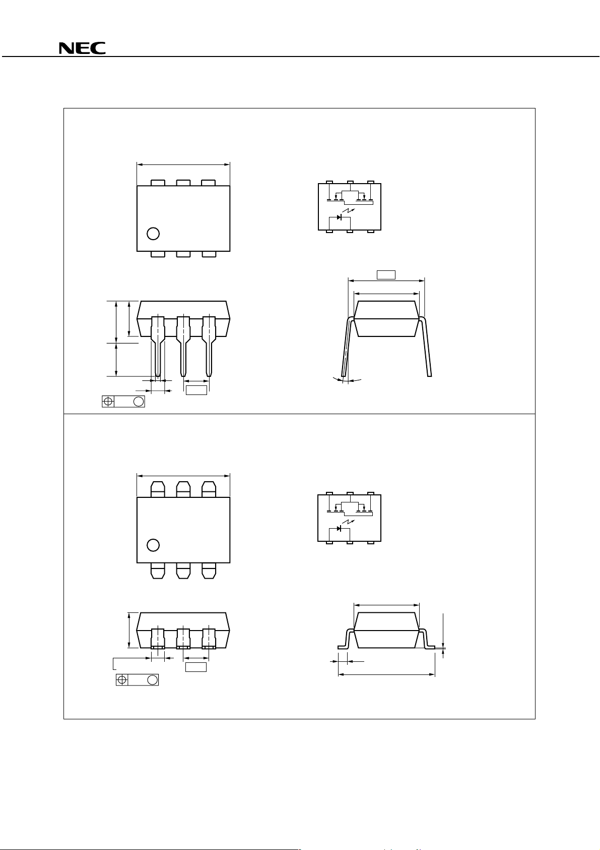
PACKAGE DIMENSIONS (in millimeters)
PS7360-1A,PS7360L-1A
PS7360-1A
4.15±0.3
3.3±0.3
0.5±0.1
1.34±0.1
0.25 M
3.5±0.3
9.25±0.5
2.54
PS7360L-1A
TOP VIEW
654
123
7.62
6.5±0.5
0 to 15˚
1. LED Anode
2. LED Cathode
3. NC
4. MOS FET Drain
5. MOS FET Source
6. MOS FET Drain
3.5±0.3
1.34±0.1
0.25 M
9.25±0.5
654
123
2.54
TOP VIEW
6.5±0.5
0.9±0.25
9.60±0.4
1. LED Anode
2. LED Cathode
3. NC
4. MOS FET Drain
5. MOS FET Source
6. MOS FET Drain
+0.10
–0.05
0.10
2
Data Sheet PN10310EJ02V0DS
Page 3
PS7360-1A,PS7360L-1A
<R>
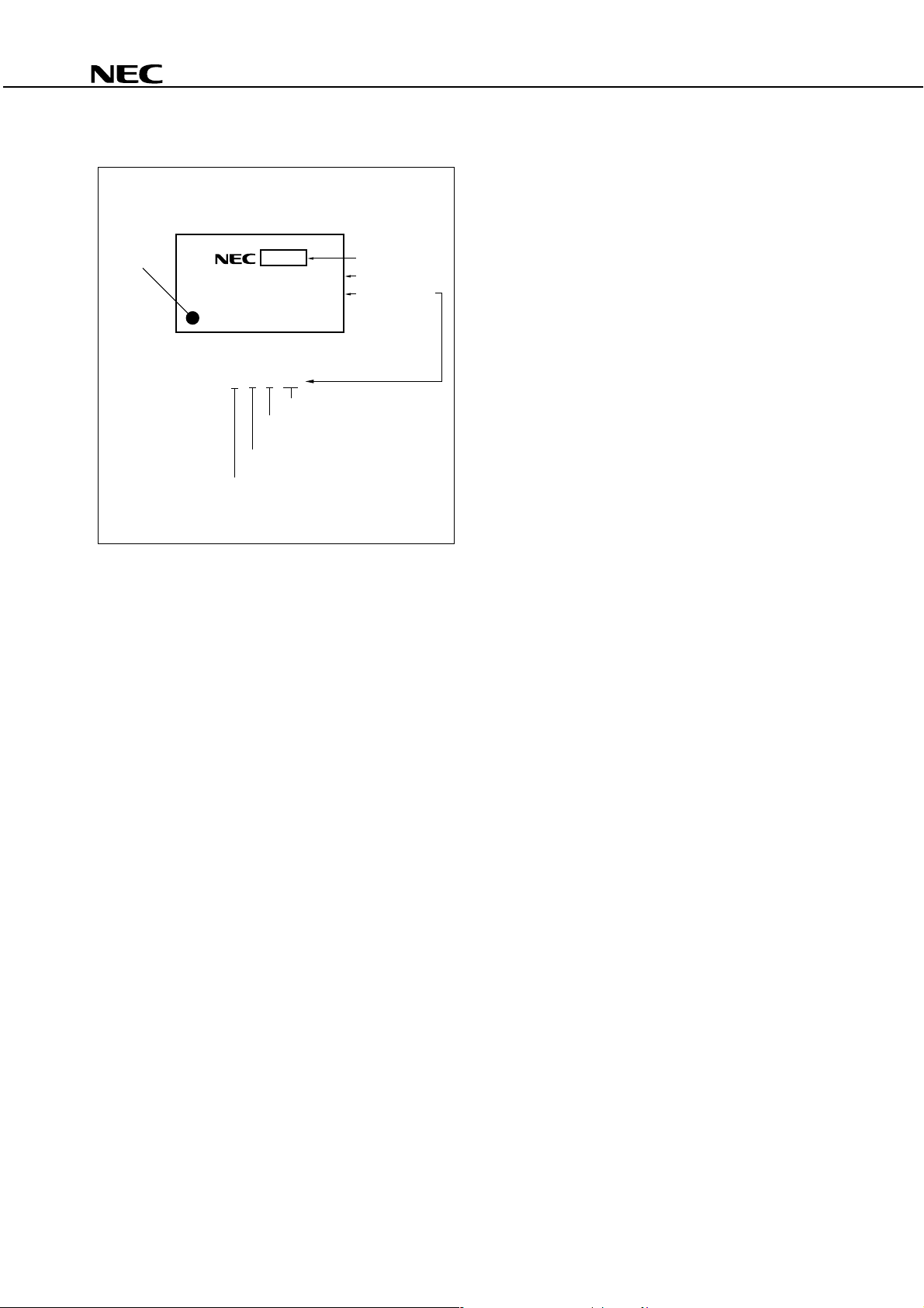
MARKING EXAMPLE
No. 1 pin
Mark
PS7360-1A
NL601
Rank Code
LN
6
01
Week Assembled
Year Assembled
(Last 1 Digit)
In-house Code
(L: Pb-Free)
Country Assembled
Type Number
Assembly Lot
Data Sheet PN10310EJ02V0DS
3
Page 4

PS7360-1A,PS7360L-1A
<R>
ORDERING INFORMATION
Part Number Order Number Solder Plating
Specification
PS7360-1A PS7360-1A-A Pb-Free Magazine case 50 pcs Standard products PS7360-1A
PS7360L-1A PS7360L-1A-A (UL, BSI, CSA, SEMKO,
PS7360L-1A-E3 PS7360L-1A-E3-A Embossed Tape 1 000 pcs/reel DEMKO, NEMKO,
PS7360L-1A-E4 PS7360L-1A-E4-A FIMKO approved)
*1 For the application of the Safety Standard, following part number should be used.
Packing Style Safety Standard
Approval
Application Part
Number
*1
4
Data Sheet PN10310EJ02V0DS
Page 5
PS7360-1A,PS7360L-1A
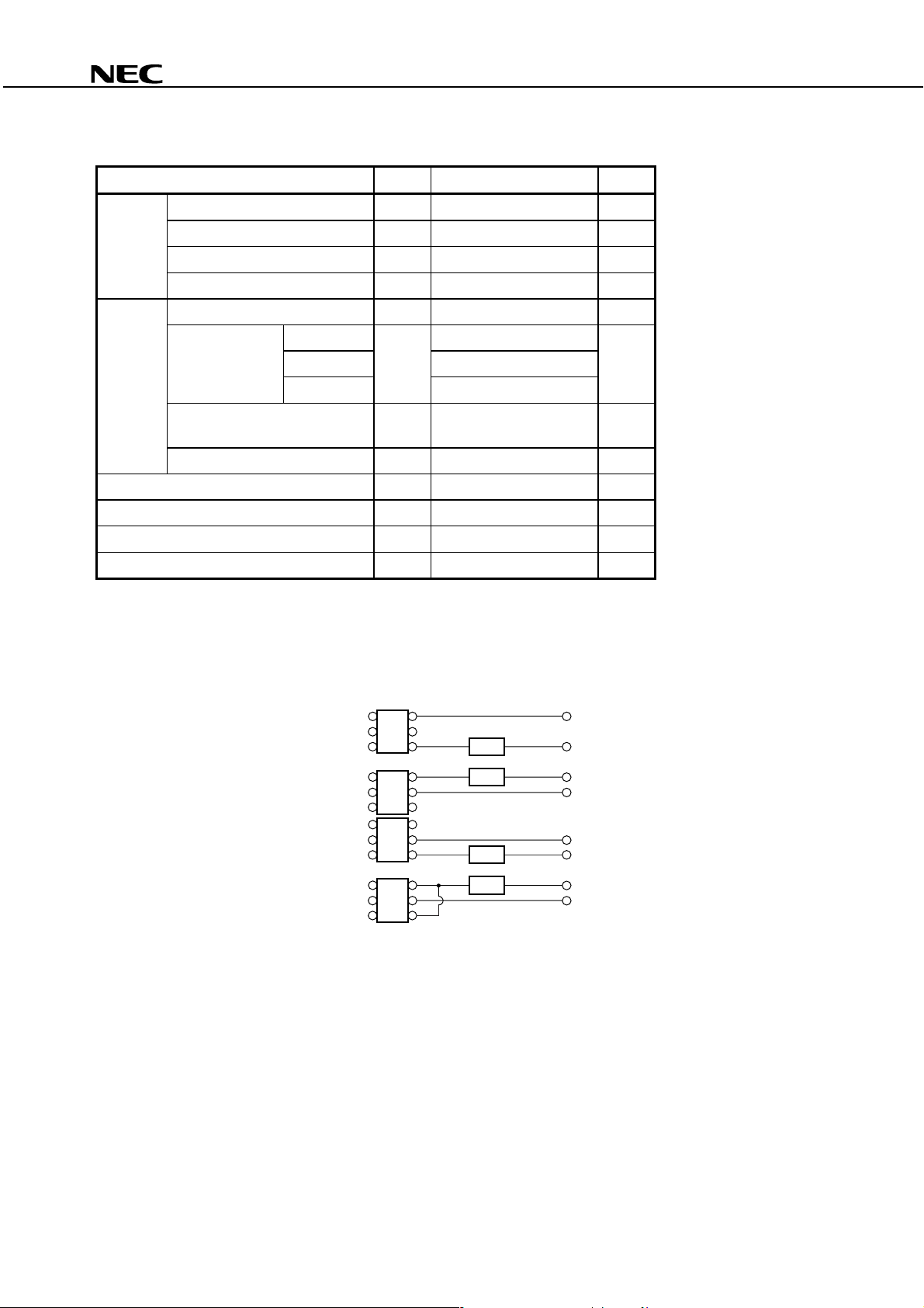
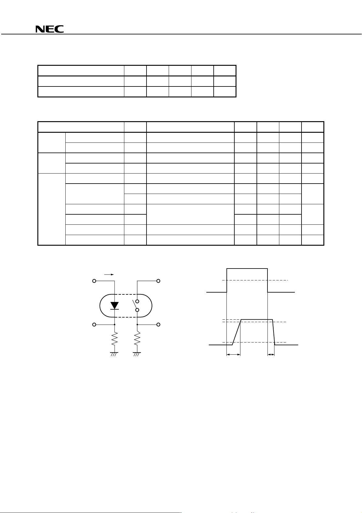
ABSOLUTE MAXIMUM RATINGS (TA = 25°C, unless otherwise specified)
Parameter Symbol Ratings Unit
Diode Forward Current (DC) IF 50 mA
Reverse Voltage VR 5.0 V
Power Dissipation PD 50 mW
Peak Forward Current
MOS FET Break Down Voltage VL 600 V
Continuous Connection A IL 90 (120) mA
Load Current
*2
Connection C 200 (210)
Pulse Load Current
(AC/DC Connection)
Power Dissipation PD 560 mW
Isolation Voltage
*4
BV 3 750 Vr.m.s.
Total Power Dissipation PT 610 mW
Operating Ambient Temperature TA −40 to +85 °C
Storage Temperature Tstg −40 to +125 °C
*1 PW = 100
*2 Conditions: I
Conditions: I
µ
s, Duty Cycle = 1%
F ≥ 2 mA.
F ≥ 5 mA. Load current ( ) value is.
The following types of load connections are available.
*3 PW = 100 ms, 1 shot
*4 AC voltage for 1 minute at T
Pins 1-3 shorted together, 4-6 shorted together.
*1
IFP 1 A
Connection B 130 (160)
*3
Connection A VL (AC/DC)
Connection B
Connection C
A = 25°C, RH = 60% between input and output
ILP 250 mA
1
25
3
1
2
6
I
L
4
6
5
L
L
L
I
+
V
L
(DC)
–
43
1
2
3
1
2
3
6
5
I
L
4
6
5
4
L
I
L
L
IL + I
I
L
L
–
V
L
(DC)
+
+
V
L
(DC)
–
Data Sheet PN10310EJ02V0DS
5
Page 6
PS7360-1A,PS7360L-1A
RECOMMENDED OPERATING CONDITIONS (TA = 25°C)
Parameter Symbol MIN. TYP. MAX. Unit
LED Operating Current IF 2 10 20 mA
LED Off Voltage VF 0 0.5 V
ELECTRICAL CHARACTERISTICS (TA = 25°C)
Parameter Symbol Conditions MIN. TYP. MAX. Unit
Diode Forward Voltage VF IF = 10 mA 1.2 1.4 V
Reverse Current IR VR = 5 V 5.0
MOS FET Off-state Leakage Current ILoff VD = 600 V 0.03 1.0
Output Capacitance Cout VD = 0 V, f = 1 MHz 110 pF
Coupled LED On-state Current IFon IL = 90 mA 2.0 mA
On-state Resistance Ron1 IF = 10 mA, IL = 10 mA 41 50
Ron2 IF = 10 mA, IL = 90 mA, t ≤ 10 ms 33 45
Turn-on Time
Turn-off Time
Isolation Resistance RI-O VI-O = 1.0 kVDC 109
Isolation Capacitance CI-O V = 0 V, f = 1 MHz 1.1 pF
*1 Test Circuit for Switching Time
Pulse Input
*1, 2
ton IF = 10 mA, VO = 5 V, RL = 2 kΩ, 0.6 2.0 ms
*1, 2
toff PW ≥ 10 ms 0.03 0.2
I
F
V
L
Input
50 %
µ
A
µ
A
Ω
Ω
<R>
Input monitor monitorV
R
in
R
L
VO = 5 V
Output
t
on
t
off
O
90 %
10 %
*2 The turn-on time and turn-off time are specified as input-pulse width ≥ 10 ms.
Be aware that when the device operates with an input-pulse width less than 10 ms, the turn-on time and turn-off
time will increase.
0
6
Data Sheet PN10310EJ02V0DS
Page 7

PS7360-1A,PS7360L-1A
TYPICAL CHARACTERISTICS (TA = 25°C, unless otherwise specified)
MAXIMUM FORWARD CURRENT vs.
AMBIENT TEMPERATURE
100
MAXIMUM LOAD CURRENT vs.
AMBIENT TEMPERATURE
150
(mA)
80
F
60
40
20
Maximum Forward Current I
0
Ambient Temperature T
FORWARD VOLTAGE vs.
AMBIENT TEMPERATURE
1.6
1.4
(V)
F
1.2
85
7550250–25
A
(˚C)
IF = 50 mA
30 mA
20 mA
10 mA
5 mA
1 mA
100
125
(mA)
L
100
75
50
25
Maximum Load Current I
0
Ambient Temperature TA (˚C)
OUTPUT CAPACITANCE vs.
APPLIED VOLTAGE
250
200
(pF)
out
150
100
85
7550250–25
f = 1 MHz
100
1.0
Forward Voltage V
0.8
Ambient Temperature T
A
(˚C)
7550250–25
100
OFF-STATE LEAKAGE CURRENT vs.
APPLIED VOLTAGE
–3
10
–4
(A)
10
Loff
–5
10
–6
10
–7
10
–8
10
Off-state Leakage Current I
–9
10
200
Applied Voltage VD (V)
Remark The graphs indicate nominal characteristics.
TA = 85 ˚C
25 ˚C
400
6005003001000
50
Output Capacitance C
0
D
Applied Voltage V
(V)
LOAD CURRENT vs. LOAD VOLTAGE
150
100
(mA)
L
Load Current I
–2.0 2.0–4.0 4.00
50
–50
–100
–150
Load Voltage VL (V)
10080604020
IF = 10 mA
120
Data Sheet PN10310EJ02V0DS
7
Page 8

NORMALIZED ON-STATE RESISTANCE vs.
AMBIENT TEMPERATURE
3.0
on
2.5
2.0
Normalized to 1.0
at T
A
= 25 ˚C,
F
= 10 mA,
I
I
L
= 10 mA
PS7360-1A,PS7360L-1A
ON-STATE RESISTANCE DISTRIBTION
30
25
20
n = 50 pcs,
F
= 10 mA,
I
I
L
= 10 mA
1.5
1.0
0.5
Normalized On-state Resistance R
0.0
Ambient Temperature T
A
(˚C)
7550250–25
TURN-ON TIME vs. FORWARD CURRENT
8.0
6.0
(ms)
on
4.0
2.0
Turn-on Time t
0
Forward Current IF (mA)
V
O
= 5 V
100
302010
15
Number (pcs)
10
5
0
On-state Resistance R
4140
on
(Ω)
TURN-OFF TIME vs. FORWARD CURRENT
0.5
0.4
(ms)
off
0.3
0.2
Turn-off Time t
0.1
0
Forward Current IF (mA)
V
O
= 5 V
302010
TURN-ON TIME DISTRIBUTION
30
25
20
15
Number (pcs)
10
5
0
0.5 0.6
Turn-on Time ton (ms)
Remark The graphs indicate nominal characteristics.
8
n = 50 pcs,
F
= 10 mA,
I
V
O
= 5 V
Data Sheet PN10310EJ02V0DS
TURN-OFF TIME DISTRIBUTION
30
25
20
15
Number (pcs)
10
5
0
0.03 0.05
Turn-off Time t
off
(ms)
n = 50 pcs,
F
= 10 mA,
I
O
= 5 V
V
Page 9

PS7360-1A,PS7360L-1A
NORMALIZED TURN-ON TIME vs.
AMBIENT TEMPERATURE
3.0
on
2.5
2.0
1.5
1.0
0.5
Normalized Turn-on Time t
0.0
0–25 25 50 75
Ambient Temperature TA (˚C)
Remark The graphs indicate nominal characteristics.
Normalized to 1.0
A
= 25 ˚C,
at T
F
= 10 mA,
I
VO = 5 V
100
NORMALIZED TURN-OFF TIME vs.
AMBIENT TEMPERATURE
3.0
off
2.5
2.0
1.5
1.0
0.5
Normalized Turn-off Time t
0.0
0–25 25 50 75
Ambient Temperature TA (˚C)
Normalized to 1.0
at T
IF = 10 mA,
VO = 5 V
A
= 25 ˚C,
100
Data Sheet PN10310EJ02V0DS
9
Page 10
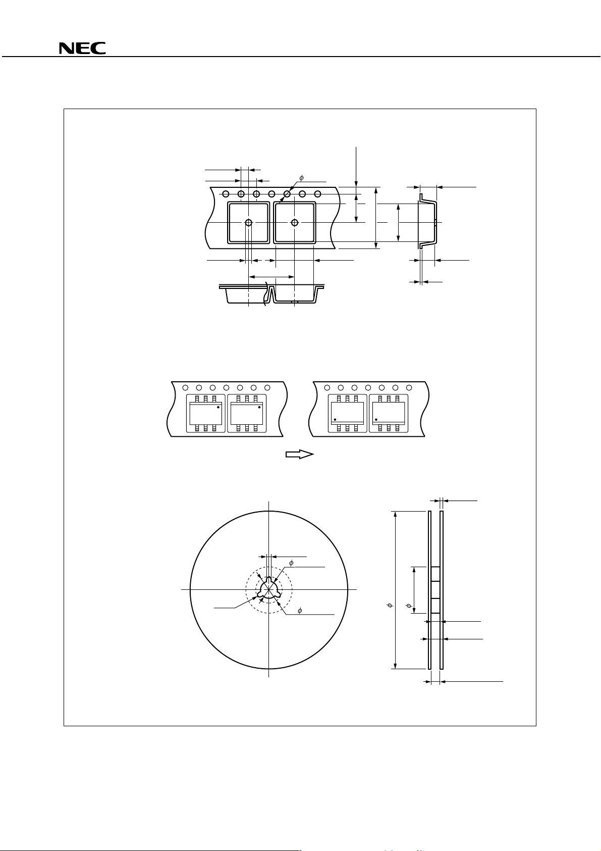
TAPING SPECIFICATIONS (in millimeters)
Outline and Dimensions (Tape)
PS7360-1A,PS7360L-1A
Tape Direction
PS7360L-1A-E3 PS7360L-1A-E4
2.0±0.1
4.0±0.1
1.55±0.1
12.0±0.1
1.5
+0.1
–0
10.4±0.1
1.75±0.1
7.5±0.1
16.0±0.3
4.5 MAX.
10.3±0.1
4.0±0.1
0.3
Outline and Dimensions (Reel)
R 1.0
Packing: 1 000 pcs/reel
2.0±0.5
13.0±0.2
21.0±0.8
330±2.0
100±1.0
2.0±0.5
17.5±1.0
21.5±1.0
15.9 to 19.4
Outer edge of
flange
10
Data Sheet PN10310EJ02V0DS
Page 11

PS7360-1A,PS7360L-1A
RECOMMENDED SOLDERING CONDITIONS
(1) Infrared reflow soldering
• Peak reflow temperature 260°C or below (package surface temperature)
• Time of peak reflow temperature 10 seconds or less
• Time of temperature higher than 220°C 60 seconds or less
• Time to preheat temperature from 120 to 180°C 120±30 s
• Number of reflows Two
• Flux Rosin flux containing small amount of chlorine (The flux with a
maximum chlorine content of 0.2 Wt% is recommended.)
Recommended Temperature Profile of Infrared Reflow
(heating)
to 10 s
260˚C MAX.
220˚C
to 60 s
<R>
180˚C
120˚C
Package Surface Temperature T (˚C)
120±30 s
(preheating)
Time (s)
(2) Wave soldering
• Temperature 260°C or below (molten solder temperature)
• Time 10 seconds or less
• Preheating conditions 120°C or below (package surface temperature)
• Number of times One
• Flux Rosin flux containing small amount of chlorine (The flux with a maximum chlorine
content of 0.2 Wt% is recommended.)
(3) Soldering by soldering iron
• Peak temperature (lead part temperature) 350°C or below
• Time (each pins) 3 seconds or less
• Flux Rosin flux containing small amount of chlorine (The flux with a
maximum chlorine content of 0.2 Wt% is recommended.)
(a) Soldering of leads should be made at the point 1.5 to 2.0 mm from the root of the lead.
(b) Please be sure that the temperature of the package would not be heated over 100°C.
Data Sheet PN10310EJ02V0DS
11
Page 12

<R>
<R>
PS7360-1A,PS7360L-1A
(4) Cautions
• To avoid quality degradation, assembling within 1 month after take this device out from covered pack is required.
(Storage conditions 25°C, 65%RH MAX.)
• Fluxes
Avoid removing the residual flux with freon-based and chlorine-based cleaning solvent.
USAGE CAUTIONS
1. Protect against static electricity when handling.
2. Avoid storage at a high temperature and high humidity.
12
Data Sheet PN10310EJ02V0DS
Page 13
PS7360-1A,PS7360L-1A
•
The information in this document is current as of September, 2006. The information is subject to
change without notice. For actual design-in, refer to the latest publications of NEC Electronics data
sheets or data books, etc., for the most up-to-date specifications of NEC Electronics products. Not
all products and/or types are available in every country. Please check with an NEC Electronics sales
representative for availability and additional information.
No part of this document may be copied or reproduced in any form or by any means without the prior
•
written consent of NEC Electronics. NEC Electronics assumes no responsibility for any errors that may
appear in this document.
•
NEC Electronics does not assume any liability for infringement of patents, copyrights or other intellectual
property rights of third parties by or arising from the use of NEC Electronics products listed in this document
or any other liability arising from the use of such products. No license, express, implied or otherwise, is
granted under any patents, copyrights or other intellectual property rights of NEC Electronics or others.
Descriptions of circuits, software and other related information in this document are provided for illustrative
•
purposes in semiconductor product operation and application examples. The incorporation of these
circuits, software and information in the design of a customer's equipment shall be done under the full
responsibility of the customer. NEC Electronics assumes no responsibility for any losses incurred by
customers or third parties arising from the use of these circuits, software and information.
•
While NEC Electronics endeavors to enhance the quality, reliability and safety of NEC Electronics products,
customers agree and acknowledge that the possibility of defects thereof cannot be eliminated entirely. To
minimize risks of damage to property or injury (including death) to persons arising from defects in NEC
Electronics products, customers must incorporate sufficient safety measures in their design, such as
redundancy, fire-containment and anti-failure features.
•
NEC Electronics products are classified into the following three quality grades: "Standard", "Special" and
"Specific".
The "Specific" quality grade applies only to NEC Electronics products developed based on a customerdesignated "quality assurance program" for a specific application. The recommended applications of an NEC
Electronics product depend on its quality grade, as indicated below. Customers must check the quality grade of
each NEC Electronics product before using it in a particular application.
"Standard":
"Special":
"Specific":
Computers, office equipment, communications equipment, test and measurement equipment, audio
and visual equipment, home electronic appliances, machine tools, personal electronic equipment
and industrial robots.
Transportation equipment (automobiles, trains, ships, etc.), traffic control systems, anti-disaster
systems, anti-crime systems, safety equipment and medical equipment (not specifically designed
for life support).
Aircraft, aerospace equipment, submersible repeaters, nuclear reactor control systems, life
support systems and medical equipment for life support, etc.
The quality grade of NEC Electronics products is "Standard" unless otherwise expressly specified in NEC
Electronics data sheets or data books, etc. If customers wish to use NEC Electronics products in applications
not intended by NEC Electronics, they must contact an NEC Electronics sales representative in advance to
determine NEC Electronics' willingness to support a given application.
(Note)
(1)
"NEC Electronics" as used in this statement means NEC Electronics Corporation and also includes its
majority-owned subsidiaries.
(2)
"NEC Electronics products" means any product developed or manufactured by or for NEC Electronics (as
defined above).
M8E 02. 11-1
Data Sheet PN10310EJ02V0DS
13
Page 14

PS7360-1A,PS7360L-1A
Caution GaAs Products
This product uses gallium arsenide (GaAs).
GaAs vapor and powder are hazardous to human health if inhaled or ingested, so please observe
the following points.
• Follow related laws and ordinances when disposing of the product. If there are no applicable laws
and/or ordinances, dispose of the product as recommended below.
1. Commission a disposal company able to (with a license to) collect, transport and dispose of
materials that contain arsenic and other such industrial waste materials.
2. Exclude the product from general industrial waste and household garbage, and ensure that the
product is controlled (as industrial waste subject to special control) up until final disposal.
• Do not burn, destroy, cut, crush, or chemically dissolve the product.
• Do not lick the product or in any way allow it to enter the mouth.
For further information, please contact
NEC Compound Semiconductor Devices Hong Kong Limited
E-mail: contact@ncsd-hk.necel.com
Hong Kong Head Office TEL: +852-3107-7303 FAX: +852-3107-7309
Taipei Branch Office TEL: +886-2-8712-0478 FAX: +886-2-2545-3859
Korea Branch Office TEL: +82-2-558-2120 FAX: +82-2-558-5209
NEC Electronics (Europe) GmbH http://www.eu.necel.com/
TEL: +49-211-6503-0 FAX: +49-211-6503-1327
California Eastern Laboratories, Inc. http://www.cel.com/
TEL: +1-408-988-3500 FAX: +1-408-988-0279
Compound Semiconductor Devices Division
NEC Electronics Corporation
URL: http://www.ncsd.necel.com/
0604
 Loading...