


DATA SHEET
PHOTOCOUPLER
PS2562-1,PS2562L-1,PS2562L1-1,PS2562L2-1
HIGH ISOLATION VOLTAGE
DARLINGTON TRANSISTOR TYPE
MULTI PHOTOCOUPLER SERIES
DESCRIPTION
The PS2562-1 is optically coupled isolators containing a GaAs light emitting diode and an NPN silicon darlington
connected phototransistor.
The PS2562-1 is in a plastic DIP (Dual In-line Package) and the PS2562L-1 is lead bending type (Gull-wing) for
surface mount.
The PS2562L1-1 is lead bending type for long creepage distance.
The PS2562L2-1 is lead bending type for long creepage distance (Gull-wing) for surface mount.
FEATURES
• High isolation voltage (BV = 5 000 Vr.m.s.)
• High current transfer ratio (CTR = 2 000 % TYP.)
• High-speed switching (t
• Ordering number of tape product: PS2562L-1-E3, E4, F3, F4, PS2562L2-1-E3, E4
• Safety standards
• UL approved: File No. E72422
• BSI approved: No. 7112/7420
• CSA approved: No. CA 101391
• NEMKO approved: No. P03200272
• SEMKO approved: No. 303059
• DEMKO approved: No. 312341
• FIMKO approved: No. FI 10620
• DIN EN60747-5-2 (VDE0884 Part2) approved (option)
APPLICATIONS
• Power supply
• Telephone/FAX.
• FA/OA equipment
• Programmable logic controller
r, tf = 100
µ
s TYP.)
−NEPOC Series−
The information in this document is subject to change without notice. Before using this document, please confirm that
this is the latest version.
Not all devices/types available in every country. Please check with local NEC Compound Semiconductor Devices
representative for availability and additional information.
Document No. PN10235EJ03V0DS (3rd edition)
Date Published March 2006 CP(K)
Printed in Japan
The mark shows major revised points.
NEC Compound Semiconductor Devices, Ltd. 1992, 2006
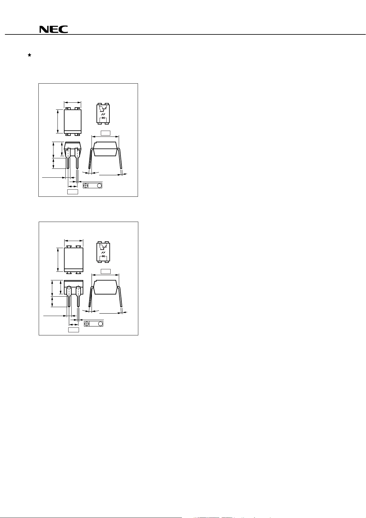
PACKAGE DIMENSIONS (UNIT : mm)
DIP Type (New package)
PS2562-1,PS2562L-1,PS2562L1-1,PS2562L2-1
6.5±0.5
4.15±0.43.2±0.4
3.5±0.3
1.25±0.15
DIP Type
6.5±0.5
PS2562-1
4.6±0.35
2.54
PS2562-1
4.6±0.5
0 to 15˚
0.50±0.10
0.25
TOP VIEW
43
1. Anode
2. Cathode
3. Emitter
4. Collector
12
7.62
+0.1
0.25
–0.05
M
TOP VIEW
43
1. Anode
2. Cathode
3. Emitter
4. Collector
12
7.62
4.15±0.43.3±0.5
1.25±0.15
3.5±0.3
2.54
0 to 15˚
0.50±0.10
0.25
0.25
M
+0.1
–0.05
2
Data Sheet PN10235EJ03V0DS
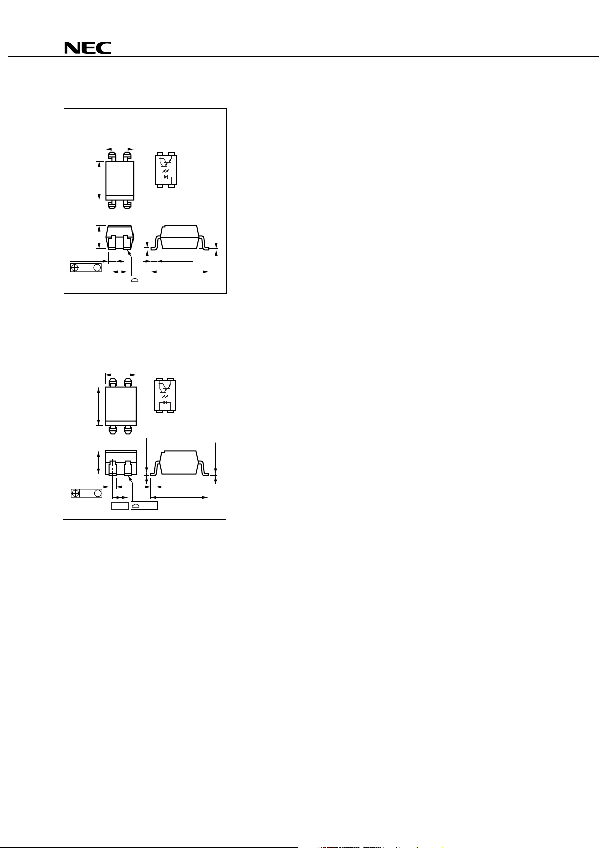
Lead Bending Type (New package)
PS2562L-1
PS2562-1,PS2562L-1,PS2562L1-1,PS2562L2-1
4.6±0.35
6.5±0.5
+0.1
–0.05
0.25
0.15
1.25±0.15
0.25
3.5±0.3
M
2.54
Lead Bending Type
PS2562L-1
4.6±0.5
6.5±0.5
TOP VIEW
43
1. Anode
2. Cathode
3. Emitter
4. Collector
12
0.9±0.25
9.60±0.4
TOP VIEW
43
1. Anode
2. Cathode
3. Emitter
4. Collector
12
+0.1
0.1
–0.05
1.25±0.15
0.25
3.5±0.3
M
2.54
+0.1
–0.05
0.25
0.15
0.9±0.25
9.60±0.4
+0.1
0.1
–0.05
Data Sheet PN10235EJ03V0DS
3
PS2562-1,PS2562L-1,PS2562L1-1,PS2562L2-1
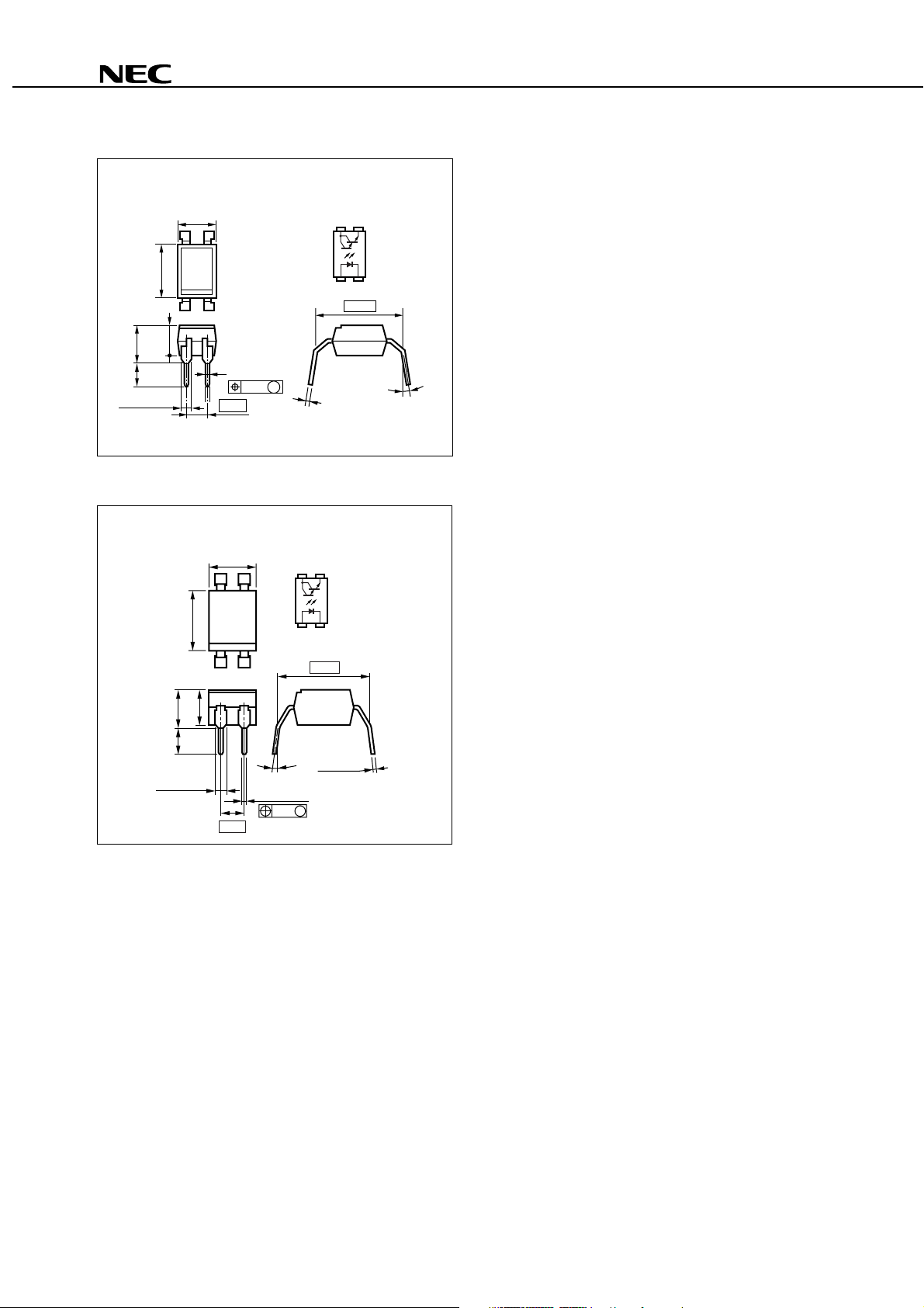
Lead Bending Type For Long Creepage Distance (New Package)
PS2562L1-1
4.6±0.35
43
6.5±0.5
12
3.5
±0.3
3.85
±0.4
3.15
±0.35
1.25±0.15
Lead Bending Type For Long Creepage Distance
0.50±0.1
0.25 M
2.54
TOP VIEW
43
12
10.16
+0.1
0.25
–0.05
1. Anode
2. Cathode
3. Emitter
4. Collector
0 to 15˚
PS2562L1-1
4.6±0.5
6.5±0.5
TOP VIEW
43
1. Anode
2. Cathode
3. Emitter
4. Collector
12
3.15±0.35 3.85±0.4
1.25±0.15
3.5±0.3
2.54
0 to 15˚
0.50±0.10
0.25
10.16
+0.1
0.25
–0.05
M
4
Data Sheet PN10235EJ03V0DS
PS2562-1,PS2562L-1,PS2562L1-1,PS2562L2-1
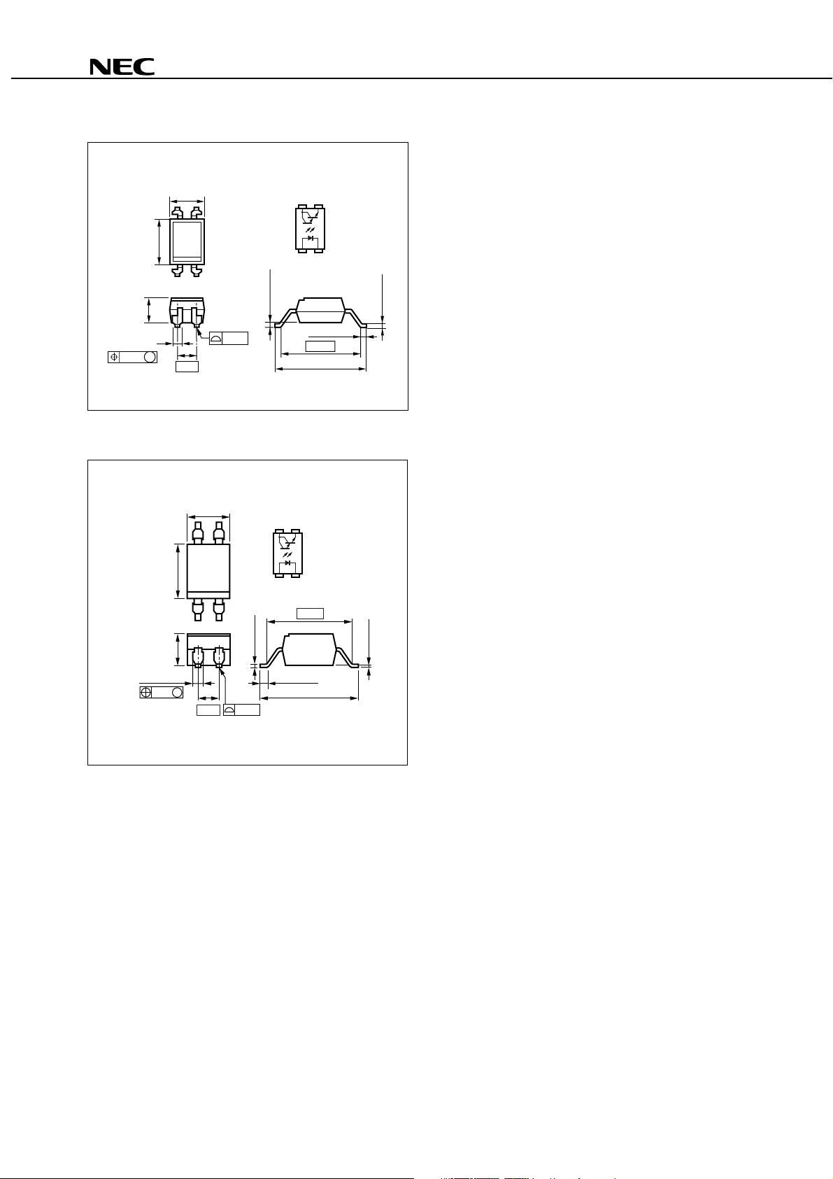
Lead Bending Type For Long Creepage Distance (Gull-Wing) (New Package)
PS2562L2-1
0.25±0.2
TOP VIEW
43
1. Anode
2. Cathode
3. Emitter
4. Collector
12
0.9±0.25
10.16
+0.2
11.8
–0.5
–0.05
+0.1
0.25
3.5±0.3
1.25±0.15
0.25 M
4.6±0.35
43
6.5±0.5
12
0.25
2.54
Lead Bending Type For Long Creepage Distance (Gull-Wing)
PS2562L2-1
4.6±0.5
6.5±0.5
TOP VIEW
43
1. Anode
2. Cathode
3. Emitter
4. Collector
12
1.25±0.15
0.25
3.5±0.3
M
2.54
0.25
+0.1
–0.05
0.25
10.16
0.9±0.25
11.8
+0.2
–0.5
0.25±0.2
Data Sheet PN10235EJ03V0DS
5
MARKING EXAMPLE
No. 1 pin
Mark
ML
CTR Rank Code
2562
ML601
6
01
Year Assembled
(Last 1 Digit)
In-house Code
PS2562-1,PS2562L-1,PS2562L1-1,PS2562L2-1
Assembly Lot
Week Assembled
Package
Standard PKG
New PKG
Made in Japan
Made in Taiwan
L
J
6
Data Sheet PN10235EJ03V0DS

PS2562-1,PS2562L-1,PS2562L1-1,PS2562L2-1
ORDERING INFORMATION
Part Number Order Number Solder Plating
Specification
Packing Style Safety Standard
Approval
Application Part
Number
*1
PS2562-1 PS2562-1-A Pb-Free Magazine case 100 pcs
PS2562L-1 PS2562L-1-A (UL, CSA, BSI,
PS2562L1-1 PS2562L1-1-A
PS2562L2-1 PS2562L2-1-A DEMKO, FIMKO
PS2562L-1-E3 PS2562L-1-E3-A Embossed Tape 1 000 pcs/reel approved)
PS2562L-1-E4 PS2562L-1-E4-A
PS2562L-1-F3 PS2562L-1-F3-A Embossed Tape 2 000 pcs/reel
PS2562L-1-F4 PS2562L-1-F4-A
PS2562L2-1-E3 PS2562L2-1-E3-A Embossed Tape 1 000 pcs/reel
PS2562L2-1-E4 PS2562L2-1-E4-A
PS2562-1-V PS2562-1-V-A Magazine case 100 pcs
PS2562L-1-V PS2562L-1-V-A
PS2562L1-1-V PS2562L1-1-V-A
PS2562L2-1-V PS2562L2-1-V-A (option)
PS2562L-1-V-E3 PS2562L-1-V-E3-A
PS2562L-1-V-E4 PS2562L-1-V-E4-A
PS2562L-1-V-F3 PS2562L-1-V-F3-A
PS2562L-1-V-F4 PS2562L-1-V-F4-A
PS2562L2-1-V-E3 PS2562L2-1-V-E3-A
PS2562L2-1-V-E4 PS2562L2-1-V-E4-A
Embossed Tape 1 000 pcs/reel
Embossed Tape 2 000 pcs/reel
Embossed Tape 1 000 pcs/reel
Standard products
NEMKO, SEMKO,
DIN EN60747-5-2
(VDE0884 Part2)
approved products
PS2562-1
*1 For the application of the Safety Standard, following part number should be used.
Data Sheet PN10235EJ03V0DS
7

PS2562-1,PS2562L-1,PS2562L1-1,PS2562L2-1
ABSOLUTE MAXIMUM RATINGS (TA = 25°C, unless otherwise specified)
Parameter Symbol Ratings Unit
Diode Reverse Voltage VR 6 V
Forward Current (DC) IF 80 mA
Power Dissipation Derating ∆PD/°C 1.5 mW/°C
Power Dissipation PD 150 mW
Peak Forward Current*1 IFP 1 A
Transistor Collector to Emitter Voltage VCEO 40 V
Emitter to Collector Voltage VECO 6 V
Collector Current IC 200 mA
Power Dissipation Derating ∆PC/°C 2.0 mW/°C
Power Dissipation PC 200 mW
Isolation Voltage*2 BV 5 000 Vr.m.s.
Operating Ambient Temperature TA –55 to +100 °C
Storage Temperature Tstg –55 to +150 °C
*1 PW = 100
*2 AC voltage for 1 minute at T
Pins 1-2 shorted together, 3-4 shorted together.
µ
s, Duty Cycle = 1%
A = 25°C, RH = 60% between input and output
8
Data Sheet PN10235EJ03V0DS

PS2562-1,PS2562L-1,PS2562L1-1,PS2562L2-1
ELECTRICAL CHARACTERISTICS (TA = 25°C)
Parameter Symbol Conditions MIN. TYP. MAX. Unit
Diode Forward Voltage VF IF = 10 mA 1.17 1.4 V
Reverse Current IR VR = 5 V 5
Terminal Capacitance Ct V = 0 V, f = 1.0 MHz 50 pF
Transistor Collector to Emitter Dark
Current
Coupled Current Transfer Ratio
Collector Saturation
Isolation Resistance RI-O VI-O = 1.0 kVDC 1011
Isolation Capacitance CI-O V = 0 V, f = 1.0 MHz 0.5 pF
Rise Time*2 tr VCC = 10 V, IC = 10 mA, RL = 100 Ω 100 µs
Fall Time*2 tf 100
*1
C/IF)
(I
Voltage
ICEO VCE = 40 V, IF = 0 mA 400 nA
CTR I
VCE(sat) IF = 1 mA, IC = 2 mA 1.0 V
F = 1 mA, VCE = 2 VDC 200 2 000 %
*1 CTR rank
K : 2 000 to (%)
L : 700 to 3 400 (%)
M : 200 to 1 000 (%)
*2 Test circuit for switching time
Pulse Input
PW = 1 ms
Duty Cycle = 1/10
I
F
50 Ω
V
V
RL = 100 Ω
CC
OUT
µ
A
Ω
Data Sheet PN10235EJ03V0DS
9

PS2562-1,PS2562L-1,PS2562L1-1,PS2562L2-1
TYPICAL CHARACTERISTICS (TA = 25 °C, unless otherwise specified)
150
(mW)
D
100
50
DIODE POWER DISSIPATION vs.
AMBIENT TEMPERATURE
1.5 mW/˚C
TRANSISTOR POWER DISSIPATION
vs. AMBIENT TEMPERATURE
200
(mW)
C
150
100
50
2 mW/˚C
Diode Power Dissipation P
0255075100 125 150
Ambient Temperature T
A
(˚C)
FORWARD CURRENT vs.
FORWARD VOLTAGE
100
50
(mA)
10
F
5
0.5
Forward Current I
0.1
T
A
= +100 ˚C
+60 ˚C
+25 ˚C
1
0.7 0.8 0.9 1.0 1.1 1.2
Forward Voltage VF (V)
1.3
COLLECTOR TO EMITTER DARK
CURRENT vs. AMBIENT TEMPERATURE
(nA)
10 000
CEO
1000
100
VCE = 2 V
5 V
10 V
24 V
40 V
0 ˚C
–25 ˚C
–55 ˚C
1.4
1.5
Transistor Power Dissipation P
0255075100 125 150
Ambient Temperature TA (˚C)
COLLECTOR CURRENT vs.
COLLECTOR TO EMITTER VOLTAGE
160
5 mA
140
120
(mA)
C
100
80
60
40
Collector Current I
20
2 mA
1 mA
IF = 0.5 mA
0
2
Collector to Emitter Voltage VCE (V)
46810
COLLECTOR CURRENT vs.
COLLECTOR SATURATION VOLTAGE
200
100
50
(mA)
C
10
5
5 mA
2 mA
1 mA
0.5 mA
10
1
Collector to Emitter Dark Current I
–50 –25 0 25 50
Ambient Temperature T
A
(˚C)
75
Remark The graphs indicate nominal characteristics.
10
Data Sheet PN10235EJ03V0DS
100
1
Collector Current I
0.5
0.2
0.4
0.6 0.8
Collector Saturation Voltage V
1.2 1.4 1.6
1.0
0.2 mA
IF = 0.1 mA
CE(sat)
(V)

PS2562-1,PS2562L-1,PS2562L1-1,PS2562L2-1
NORMALIZED CURRENT TRANSFER
RATIO vs. AMBIENT TEMPERATURE
1.4
1.2
1.0
0.8
0.6
0.4
0.2
Normalized Current Transfer Ratio CTR
–50 0–25 50
Ambient Temperature T
Normalized to 1.0
at T
A = 25 ˚C,
I
F = 1 mA, VCE = 2 V
25
A (˚C)
SWITCHING TIME vs.
LOAD RESISTANCE
1 000
µ
Switching Time t ( s)
CC = 5 V,
V
IC = 2 mA,
500
CTR = 2 280 %
tf
100
50
10
5
2
30
50 500 1 k 5 k
ts
100
Load Resistance R
tr
td
L (Ω)
75
100
CURRENT TRANSFER RATIO vs.
FORWARD CURRENT
8 000
7 000
Sample A
6 000
5 000
4 000
3 000
2 000
1 000
Current Transfer Ratio CTR (%)
0
0.1 0.5 1 5 10 30
B
C
D
Forward Current I
CURRENT TRANSFER RATIO vs.
FORWARD CURRENT
3 000
V
CE = 2 V
2 500
2 000
1 500
1 000
500
Current Transfer Ratio CTR (%)
0
Sample A
B
C
D
50 10010 500
Forward Current IF ( A)
VCE = 2 V
F (mA)
µ
SWITCHING TIME vs.
LOAD RESISTANCE
10 000
5 000
µ
1 000
500
100
50
Switching Time t ( s)
10
1 k300
500 100 k
Load Resistance RL (Ω)
5 k
Remark The graphs indicate nominal characteristics.
VCC = 5 V,
F = 1 mA,
I
tf
CTR = 2 280 %
ts
tr
td
10 k 50 k
Data Sheet PN10235EJ03V0DS
FREQUENCY RESPONSE
0
V
–5
–10
–15
Normalized Gain G
–20
0.2 0.5 1 2
RL = 100 Ω
10
5
Frequency f (kHz)
20
IF = 1 mA,
CE = 2 V
V
50 100
200
11

LONG TERM CTR DEGRADATION
1.2
1.0
0.8
0.6
0.4
CTR (Relative Value)
0.2
PS2562-1,PS2562L-1,PS2562L1-1,PS2562L2-1
IF = 1 mA
TA = 25 oC
TA = 60 oC
0
10 10
2
10
3
10
4
10
5
10
Time (Hr)
Remark The graph indicates nominal characteristics.
6
12
Data Sheet PN10235EJ03V0DS

PS2562-1,PS2562L-1,PS2562L1-1,PS2562L2-1
TAPING SPECIFICATIONS (UNIT : mm)
Outline and Dimensions (Tape)
2.0±0.1
4.0±0.1
+0.1
φ
1.5
1.75±0.1
–0
7.5±0.1
16.0±0.3
10.3±0.1
4.5 MAX.
1.55±0.1
8.0±0.1
Tape Direction
PS2562L-1-E3 PS2562L-1-E4
Outline and Dimensions (Reel)
5.3±0.1
2.0±0.5
φ
13.0±0.2
4.0±0.1
0.4
2.0±0.5
R 1.0
Packing: 1 000 pcs/reel
Data Sheet PN10235EJ03V0DS
21.0±0.8
φ
254±2.0
80.0±1.0
φ
φ
17.5±1.0
21.5±1.0
15.9 to 19.4
Outer edge of
flange
13

PS2562-1,PS2562L-1,PS2562L1-1,PS2562L2-1
Outline and Dimensions (Tape)
2.0±0.1
4.0±0.1
1.5
+0.1
–0
1.75±0.1
7.5±0.1
16.0±0.3
4.5 MAX.
10.3±0.1
1.55±0.1
8.0±0.1
Tape Direction
PS2562L-1-F3 PS2562L-1-F4
Outline and Dimensions (Reel)
5.3±0.1
2.0±0.5
φ
13.0±0.2
4.0±0.1
0.4
2.0±0.5
14
R 1.0
Packing: 2 000 pcs/reel
Data Sheet PN10235EJ03V0DS
21.0±0.8
φ
100±1.0
330±2.0
φ
φ
17.5±1.0
21.5±1.0
15.9 to 19.4
Outer edge of
flang

PS2562-1,PS2562L-1,PS2562L1-1,PS2562L2-1
Outline and Dimensions (Tape)
2.0±0.1
4.0±0.1
1.55±0.1
1.75±0.1
11.5±0.1
4.4±0.2
2.05±0.1
12.0±0.1
Tape Direction
PS2562L2-1-E3 PS2562L2-1-E4
Outline and Dimensions (Reel)
6.6±0.2
24.0±0.3
12.35±0.15
0.38
2.0±0.5
R 1.0
Packing: 1 000 pcs/reel
Data Sheet PN10235EJ03V0DS
2.0±0.5
φ
13.0±0.2
φ
21.0±0.8
330±2.0
φ
100±1.0
φ
25.5±1.0
29.5±1.0
23.9 to 27.4
Outer edge of
flange
15

PS2562-1,PS2562L-1,PS2562L1-1,PS2562L2-1
NOTES ON HANDLING
1. Recommended soldering conditions
(1) Infrared reflow soldering
• Peak reflow temperature 260°C or below (package surface temperature)
• Time of peak reflow temperature 10 seconds or less
• Time of temperature higher than 220°C 60 seconds or less
• Time to preheat temperature from 120 to 180°C 120±30 s
• Number of reflows Three
• Flux Rosin flux containing small amount of chlorine (The flux with a
maximum chlorine content of 0.2 Wt% is recommended.)
Recommended Temperature Profile of Infrared Reflow
(heating)
to 10 s
260˚C MAX.
220˚C
to 60 s
180˚C
120˚C
Package Surface Temperature T (˚C)
120±30 s
(preheating)
Time (s)
(2) Wave soldering
• Temperature 260°C or below (molten solder temperature)
• Time 10 seconds or less
• Preheating conditions 120°C or below (package surface temperature)
• Number of times One (Allowed to be dipped in solder including plastic mold portion.)
• Flux Rosin flux containing small amount of chlorine (The flux with a maximum chlorine
content of 0.2 Wt% is recommended.)
(3) Soldering by soldering iron
• Peak temperature (lead part temperature) 350°C or below
• Time (each pins) 3 seconds or less
• Flux Rosin flux containing small amount of chlorine (The flux with a
maximum chlorine content of 0.2 Wt% is recommended.)
(a) Soldering of leads should be made at the point 1.5 to 2.0 mm from the root of the lead.
(b) Please be sure that the temperature of the package would not be heated over 100°C.
16
Data Sheet PN10235EJ03V0DS

PS2562-1,PS2562L-1,PS2562L1-1,PS2562L2-1
(4) Cautions
• Fluxes
Avoid removing the residual flux with freon-based and chlorine-based cleaning solvent.
2. Cautions regarding noise
Be aware that when voltage is applied suddenly between the photocoupler’s input and output or between
collector-emitters at startup, the output transistor may enter the on state, even if the voltage is within the absolute
maximum ratings.
3. Measurement conditions of current transfer ratios (CTR), which differ according to photocoupler
Check the setting values before use, since the forward current conditions at CTR measurement differ according
to product.
When using products other than at the specified forward current, the characteristics curves may differ from the
standard curves due to CTR value variations or the like. Therefore, check the characteristics under the actual
operating conditions and thoroughly take variations or the like into consideration before use.
USAGE CAUTIONS
1. Protect against static electricity when handling.
2. Avoid storage at a high temperature and high humidity.
Data Sheet PN10235EJ03V0DS
17
PS2562-1,PS2562L-1,PS2562L1-1,PS2562L2-1
SPECIFICATION OF VDE MARKS LICENSE DOCUMENT
Parameter Symbol Speck Unit
Application classification (DIN VDE 0109)
for rated line voltages ≤ 300 Vr.m.s.
for rated line voltages ≤ 600 Vr.m.s.
IV
III
Climatic test class (DIN IEC 68 Teil 1/09.80) 55/100/21
Dielectric strength maximum operating isolation voltage
Test voltage (partial discharge test procedure a for type test and random test)
pr = 1.2 × UIORM, Pd < 5 pC
U
Test voltage (partial discharge test procedure b for all devices test)
pr = 1.6 × UIORM, Pd < 5 pC
U
IORM
U
Upr
U
pr 1 424 Vpeak
890
1 068
Highest permissible overvoltage UTR 8 000 Vpeak
Degree of pollution (DIN VDE 0109) 2
Clearance distance > 7.0 mm
Creepage distance > 7.0 mm
Comparative tracking index (DIN IEC 112/VDE 0303 part 1) CTI 175
Material group (DIN VDE 0109) III a
Storage temperature range Tstg –55 to +150 °C
Operating temperature range TA –55 to +100 °C
Isolation resistance, minimum value
IO = 500 V dc at TA = 25 °C
V
IO = 500 V dc at TA MAX. at least 100 °C
V
Safety maximum ratings (maximum permissible in case of fault, see thermal
derating curve)
Package temperature
Current (input current I
F, Psi = 0)
Power (output or total power dissipation)
Isolation resistance
IO = 500 V dc at TA = 175 °C (Tsi)
V
Ris MIN.
Ris MIN.
Tsi
Isi
Psi
Ris MIN.
10
10
175
400
700
10
12
11
9
peak
V
Vpeak
Ω
Ω
°C
mA
mW
Ω
18
Data Sheet PN10235EJ03V0DS

PS2562-1,PS2562L-1,PS2562L1-1,PS2562L2-1
When the product(s) listed in this document is subject to any applicable import or export control laws and regulation of the authority
having competent jurisdiction, such product(s) shall not be imported or exported without obtaining the import or export license.
•
The information in this document is current as of March, 2006. The information is subject to change
without notice. For actual design-in, refer to the latest publications of NEC's data sheets or data
books, etc., for the most up-to-date specifications of NEC semiconductor products. Not all products
and/or types are available in every country. Please check with an NEC sales representative for
availability and additional information.
•
No part of this document may be copied or reproduced in any form or by any means without prior
written consent of NEC. NEC assumes no responsibility for any errors that may appear in this document.
•
NEC does not assume any liability for infringement of patents, copyrights or other intellectual property rights of
third parties by or arising from the use of NEC semiconductor products listed in this document or any other
liability arising from the use of such products. No license, express, implied or otherwise, is granted under any
patents, copyrights or other intellectual property rights of NEC or others.
•
Descriptions of circuits, software and other related information in this document are provided for illustrative
purposes in semiconductor product operation and application examples. The incorporation of these
circuits, software and information in the design of customer's equipment shall be done under the full
responsibility of customer. NEC assumes no responsibility for any losses incurred by customers or third
parties arising from the use of these circuits, software and information.
•
While NEC endeavours to enhance the quality, reliability and safety of NEC semiconductor products, customers
agree and acknowledge that the possibility of defects thereof cannot be eliminated entirely. To minimize
risks of damage to property or injury (including death) to persons arising from defects in NEC
semiconductor products, customers must incorporate sufficient safety measures in their design, such as
redundancy, fire-containment, and anti-failure features.
•
NEC semiconductor products are classified into the following three quality grades:
"Standard", "Special" and "Specific". The "Specific" quality grade applies only to semiconductor products
developed based on a customer-designated "quality assurance program" for a specific application. The
recommended applications of a semiconductor product depend on its quality grade, as indicated below.
Customers must check the quality grade of each semiconductor product before using it in a particular
application.
"Standard": Computers, office equipment, communications equipment, test and measurement equipment, audio
and visual equipment, home electronic appliances, machine tools, personal electronic equipment
and industrial robots
"Special": Transportation equipment (automobiles, trains, ships, etc.), traffic control systems, anti-disaster
systems, anti-crime systems, safety equipment and medical equipment (not specifically designed
for life support)
"Specific": Aircraft, aerospace equipment, submersible repeaters, nuclear reactor control systems, life
support systems and medical equipment for life support, etc.
The quality grade of NEC semiconductor products is "Standard" unless otherwise expressly specified in NEC's
data sheets or data books, etc. If customers wish to use NEC semiconductor products in applications not
intended by NEC, they must contact an NEC sales representative in advance to determine NEC's willingness
to support a given application.
(Note)
(1) "NEC" as used in this statement means NEC Corporation, NEC Compound Semiconductor Devices, Ltd.
and also includes its majority-owned subsidiaries.
(2) "NEC semiconductor products" means any semiconductor product developed or manufactured by or for
NEC (as defined above).
M8E 00. 4 - 0110
Data Sheet PN10235EJ03V0DS
19

PS2562-1,PS2562L-1,PS2562L1-1,PS2562L2-1
Caution GaAs Products
This product uses gallium arsenide (GaAs).
GaAs vapor and powder are hazardous to human health if inhaled or ingested, so please observe
the following points.
• Follow related laws and ordinances when disposing of the product. If there are no applicable laws
and/or ordinances, dispose of the product as recommended below.
1. Commission a disposal company able to (with a license to) collect, transport and dispose of
materials that contain arsenic and other such industrial waste materials.
2. Exclude the product from general industrial waste and household garbage, and ensure that the
product is controlled (as industrial waste subject to special control) up until final disposal.
• Do not burn, destroy, cut, crush, or chemically dissolve the product.
• Do not lick the product or in any way allow it to enter the mouth.
For further information, please contact
NEC Compound Semiconductor Devices, Ltd. http://www.ncsd.necel.com/
E-mail: salesinfo@ml.ncsd.necel.com (sales and general)
techinfo@ml.ncsd.necel.com (technical)
Sales Division TEL: +81-44-435-1573 FAX: +81-44-435-1579
NEC Compound Semiconductor Devices Hong Kong Limited
E-mail: ncsd-hk@elhk.nec.com.hk (sales, technical and general)
Hong Kong Head Office
Taipei Branch Office
Korea Branch Office
NEC Electronics (Europe) GmbH http://www.ee.nec.de/
TEL: +49-211-6503-0 FAX: +49-211-6503-1327
California Eastern Laboratories, Inc. http://www.cel.com/
TEL: +1-408-988-3500 FAX: +1-408-988-0279
TEL: +852-3107-7303
TEL: +886-2-8712-0478
TEL: +82-2-558-2120
FAX: +852-3107-7309
FAX: +886-2-2545-3859
FAX: +82-2-558-5209
0504
 Loading...