How it Works
Log In / Sign Up
Buy Points
How it Works
FAQ
Contact Us
Questions and Suggestions
Users
Datasheet
Loading...
P
PD65P12LA
PD65P12MA
PD65P13HA
PD65P13LA
PD65P13MA
PD65P14HA
PD65P14LA
PD65P14MA
PD65P23HA
PD65P23LA
PD65P23MA
PD65P24HA
PD65P24LA
PD65P24MA
PD65P25HA
PD65P25MA
PD65P30HA
PD65P30MA
PD65P31HA
PD65P31LA
PD65P31MA
PD65P32HA
PD65P32LA
PD65P32MA
PD65P33HA
PD65P33LA
PD65P33MA
PD65P39HA
PD65P39LA
PD65P39MA
PD65P40HA
PD65P40LA
PD65P40MA
PD700
PD7000
PD7007
PD7010
2
PD70732
PD70F120
PD70F160
PD70F40
PD70F80
PD75064
PD75064A
PD75066
PD75066A
PD75068
PD75068A
PD7564A
PD7564AA
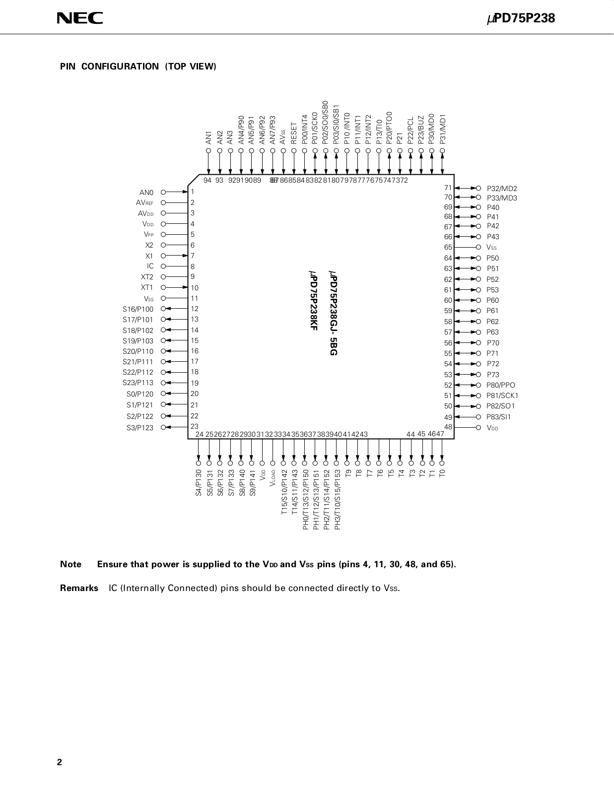
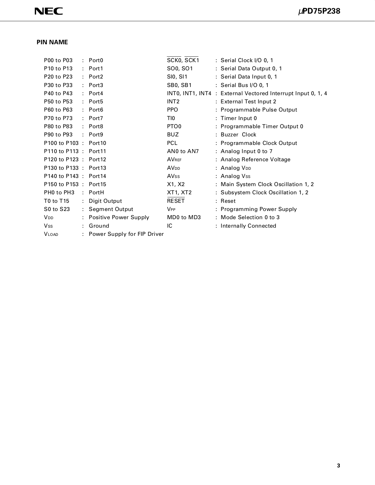
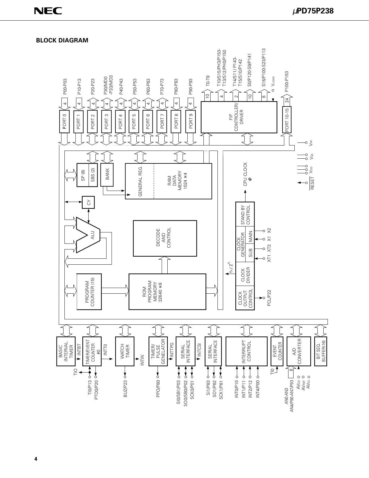
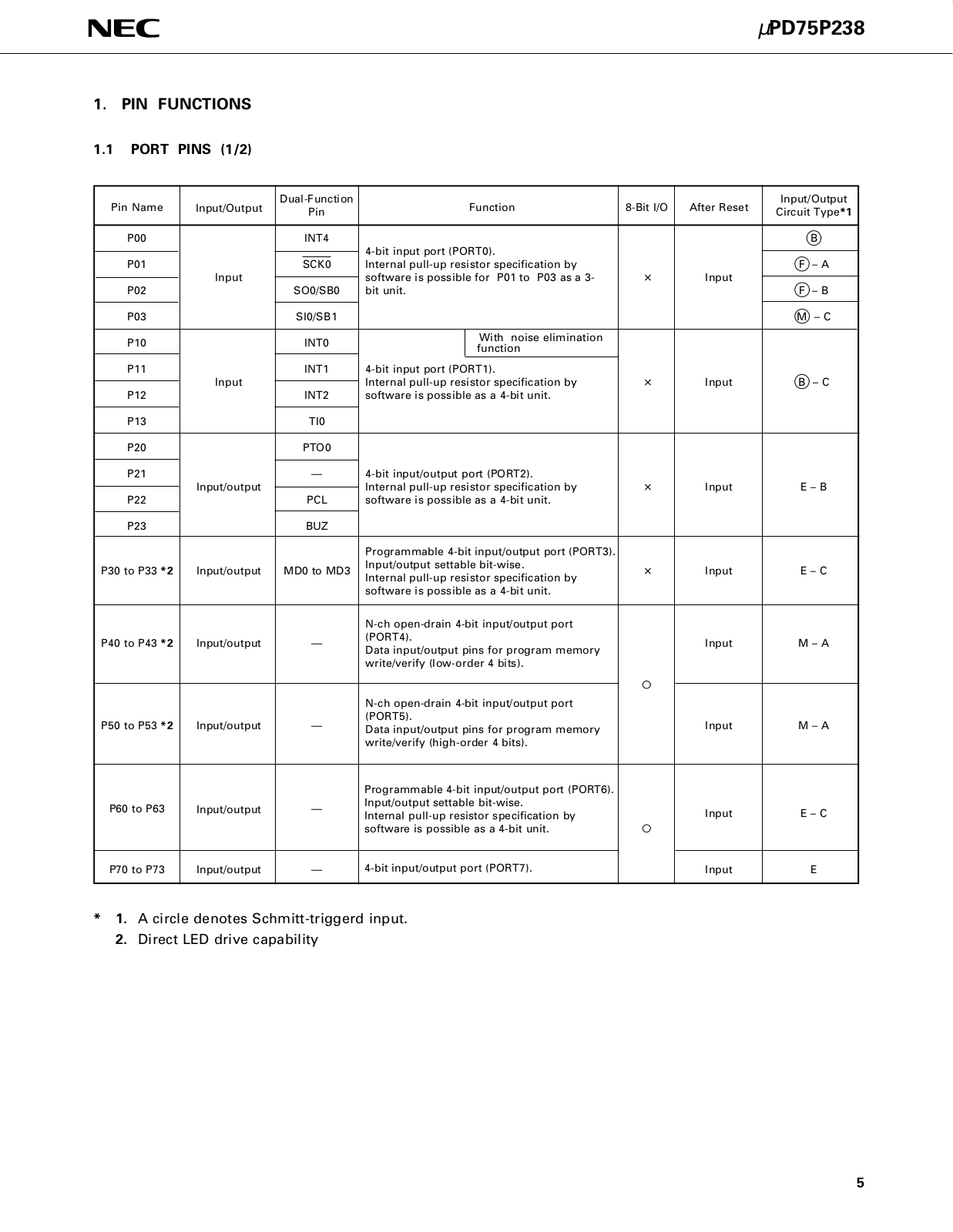
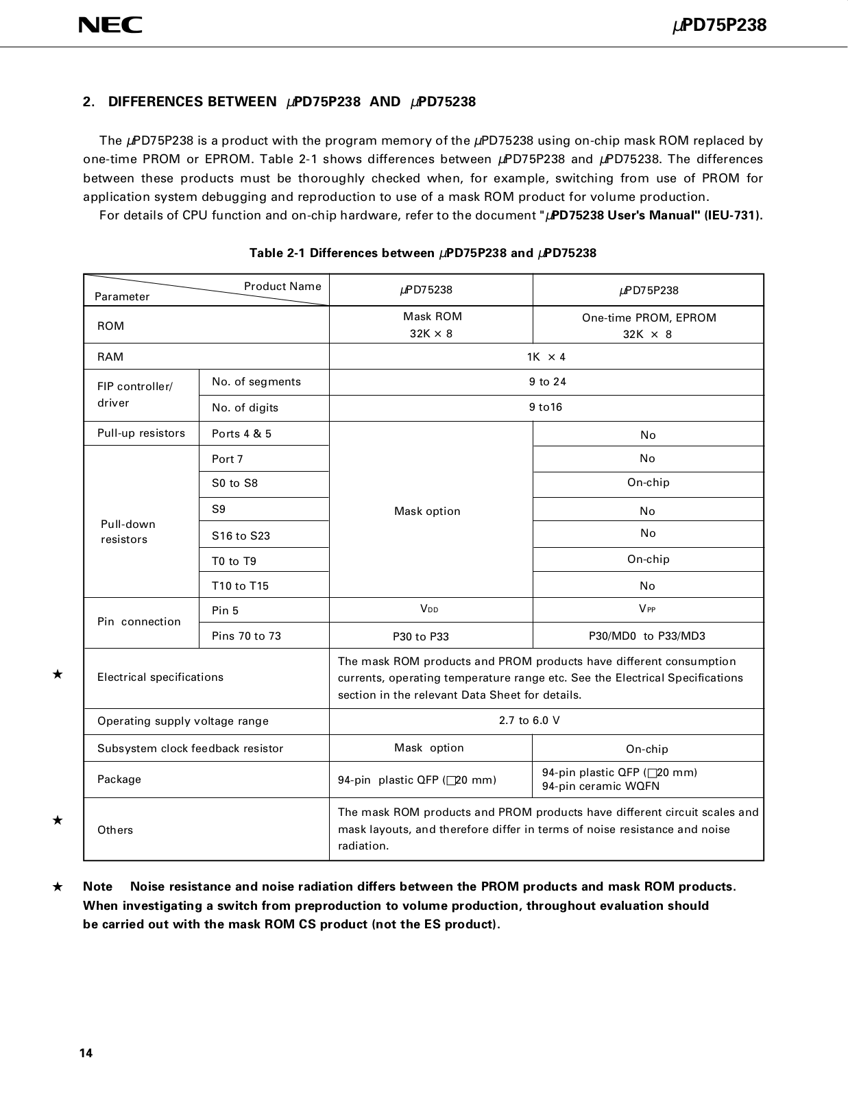
PD75P238
PD780031AY
PD780032AY
PD780033AY
PD780034AY
PD784224
PD784224Y
PD784225
PD784225Y
PD784907
PD784908
PD784927
PD784927Y
PD784928
PD784928Y
PD8042
PD8932
PD8933
PD90F120
PD90F160
PD90F40
PD90F80
PD90GB120
PD90GB160
PD90HB40
PD90HB80
PDA2446-B-AP
PDA2446-B-AS
PDA2446-B-SF
PDA2446-B-US
PDA2446-D-AP
PDA2446-D-SF
PDA2446-D-US
PDA54-11EWA
PDA54-11GWA
PDA54-11HWA
PDA54-11SRWA
PDA54-11YWA
PDA54-12EWA
PDA54-12GWA
PDA54-12HWA
PDA54-12SRWA
PDA54-12YWA
pdb-3520
PDC1602M03S
PDC54-11EWA
PDC54-11GWA
PDC54-11HWA
PDC54-11SRWA
PDC54-11YWA
Loading...
Loading...
Nothing found
PD75P238
Datasheet (NEC)
50 pgs
400.2 Kb
0
Table of contents
Loading...
Datasheet PD75P238 Datasheet (NEC)
...
Datasheet Datasheet (NEC)
Download
Specifications and Main Features
Frequently Asked Questions
User Manual
Download
Loading...
+
hidden pages
Unhide
You need points to download manuals.
1 point = 1 manual.
You can buy points or you can get point for every manual you upload.
Buy points
Upload your manuals


")