


DATA SHEET
MOS Integrated Circuit
µ
PD70732
V810
TM
32-BIT MICROPROCESSOR
The µPD70732 (a.k.a. V810) microprocessor is NEC’s first microprocessor of the V810 familyTM for embedded
control applications.
The V810 employs a RISC architecture for embedded control applications. This product has high-speed real
time response, high-speed integer operation instruction, bit string instruction, floating-point operation instruction,
and significantly high cost performance is realized for applications such as facsimile, digital PPC, word processor,
image processor, real time control device, etc.
The functions are described in detail in the following User’s Manuals, which should be read before
starting design work.
TM
• V805
• V810 Family User’s Manual Architecture : U10082E
Features
, V810 User’s Manual Hardware : U10661E
High-performance 32-bit architecture for embedded control application
• 32-bit separate address/data bus
• 1-Kbyte cache memory
• Pipeline structure of 1 clock pitch
• 16-bit fixed instructions (with some exceptions)
• 32-bit general-purpose registers: 32
• 4-Gbyte linear address space
• Register/flag hazard interlocked by hardware
Dynamic bus sizing function (16 bits)
16-bit bus fixing function
16-bit bus system can be configured.
Instructions ideal for various application fields
• Floating-point operation instructions (based upon IEEE754 data format)
• Bit string instructions
16 levels of high-speed interrupt responses
Clock can be stopped by internal static operation
Maximum operating frequency: 16/20/25 MHz
Low voltage: VDD = 2.7 to 3.6 V (Max. 16 MHz)
V
DD = 2.2 to 3.6 V (Max. 10 MHz)
Small package versions available (14 x 14 mm fine-pitch TQFP)
★
The information in this document is subject to change without notice.
Document No. U10691EJ3V0DS00 (3rd edition)
Date Published September 1996 P
Printed in Japan
The mark ★ shows major revised points.
©
1993

Ordering Information
µ
µ
µ
★
µ
µ
Pin Outline
µPD70732
Part Number Package Max. operating freq. (MHz)
PD70732GD-16-LBB 120-pin plastic QFP (28 x 28 mm) 16
PD70732GD-20-LBB 120-pin plastic QFP (28 x 28 mm) 20
PD70732GD-25-LBB 120-pin plastic QFP (28 x 28 mm) 25
PD70732GC-25-9EV 120-pin plastic TQFP (Fine pitch) (14 x 14 mm) 25
PD70732R-25 176-pin ceramic PGA (Seam weld) 25
A31 to A1
CLK
RESET
INT
INTV3 to INTV0
NMI
HLDRQ
HLDAK
V810
D31 to D0
BE3 to BE0
ST1, ST0
DA
MRQ
R/W
BCYST
BLOCK
READY
SZRQ
SIZ16B
ICHEEN
ADRSERR
2

Pin Configuration
• 120-pin plastic QFP (28 x 28 mm) (Top View)
µ
PD70732GD-xx-LBB
µPD70732
IC1
IC2
IC2
ICHEEN
NMI
INT
INTV0
INTV1
INTV2
120
119
118
117
116
115
114
113
DD
1V
112
INTV3
BLOCK
111
110
DD
V
GND
108
109
CLK
107
2IC1
3IC1
4IC1
5RESET
6D0
7D1
8D2
9GND
10D3
11D4
12GND
13D5
14D6
15D7
DD
DD
16V
17V
18D8
19D9
20D10
21D11
22D12
23GND
24D13
25D14
26D15
27D16
28D17
29D18
30GND
35GND
36D22
37D23
38D24
40D26
41D27
43D29
31VDD32D19
33D20
34D21
39D25
42D28
44D30
GND
SIZ16B
106
105
45V
46GND
104 DA
47V
DD
V
BCYST
103
102
48D31
49A31
HLDAK
ADRSERR
BE098BE197A196BE295BE394R/W93MRQ92ST1
99
101
100
50A30
51A29
52A28
54A26
55A25
53A27
56A24
57A23
58GND
59
GND
91
90
89
88
87
86
85
84
83
82
81
80
79
78
77
76
75
74
73
72
71
70
69
68
67
66
65
64
63
62
61
60V
V
DD
ST0
HLDRQ
SZRQ
READY
A2
A3
A4
A5
A6
A7
A8
GND
A9
V
DD
V
DD
GND
A10
A11
A12
A13
A14
A15
A16
A17
A18
A19
A20
A21
GND
Cautions 1. Leave the IC1 pin open.
2. Connect the IC2 pin to GND.
Remark IC: Internally Connected
DD
DD
A22
DD
3

µPD70732
★
• 120-pin plastic TQFP (Fine pitch) (14 x 14 mm) (Top View)
µ
PD70732GC-25-9EV
D9
109
42
108
43
107
44
DD
106
45
D7
105
46
D6
104
47
D5
GNDD4D3
103
102
48
49
101
50
100
51
V
D19
D20
D21
GND
D22
D23
D24
D25
D26
D27
D28
D29
D30
V
GND
V
D31
A31
A30
A29
A28
A27
A26
A25
A24
A23
GND
A22
V
GND
D18
D17
D16
D15
D14
D13
GND
D11
D10D8VDDV
D12
120
119
118
117
116
115
114
113
112
111
DD
1
110
2
3
4
5
6
7
8
9
10
11
12
13
14
DD
15
16
DD
17
18
19
20
21
22
23
24
25
26
27
28
29
DD
30
31
32
33
34
35
36
37
38
39
40
41
GNDD1D0
D2
99
98
97A196
52
54
55
53
RESET
IC1
IC1
95
94
93
56
57
58
IC1
92
59
DD
V
91
60
90
89
87
78
77
76
75
74
72
65
64
63
62
61
IC1
IC2
IC2
ICHEEN
NMI
INT
INTV0
INTV1
INTV2
INTV3
BLOCK
GND
V
DD
CLK
GND
SIZ16B
DA
V
DD
BCYST
HLDAK
ADRSERR
BE0
BE1
BE2
BE3
R/W
MRQ
ST1
GND
A2188A20
A1986A1885A1784A1683A1582A1481A1380A1279A11
GND
DD
A9
V
V
A10
GND73GND
A871A770A669A568A467A366A2
READY
SZRQ
HLDRQ
ST0
DD
V
DD
Cautions 1. VDD is power supply pin. All VDD pins should be connected to a +5V power supply (the
same power supply).
2. GND is ground pin. All GND pins should be connected to the same GND.
3. Leave the IC1 pin open.
4. Connect the IC2 pin to GND.
Remark IC: Internally Connected
4

• 176-pin ceramic PGA (Seam weld)
µ
PD70732R-25
Bottom View Top View
Insertion
guide pin
QPNML KJHGFEDCB A
15
14
13
12
11
10
µPD70732
9
8
7
6
5
4
3
2
1
A
BCDEFGHJKLMNPQ
No. 1 pin index
Remark The insertion guide pin is not included in the number of pins.
No. Signal No. Signal No. Signal No. Signal
A1 IC2 B3 GND C5 VDD D7 VDD
A2 D12 B4 D11 C6 D8 D8 VDD
A3 D13 B5 GND C7 VDD D9 GND
A4 D10 B6 D7 C8 D4 D10 IC3
A5 GND B7 VDD C9 D2 D11 IC2
A6 D6 B8 D3 C10 IC3 D12 GND
A7 IC2 B9 GND C11 VDD D13 INT
A8 D5 B10 D0 C12 IC1 D14 INTV1
A9 IC2 B11 GND C13 IC2 D15 GND
A10 D1 B12 IC1 C14 VDD E1 D27
A11 VDD B13 GND C15 NMI E2 D25
A12 RESET B14 IC1 D1 D23 E3 D21
A13 IC1 B15 ICHEEN D2 D22 E4 D19
A14 IC1 C1 VDD D3 D20 E12 IC3
A15 IC2 C2 VDD D4 GND E13 INTV0
B1 D17 C3 D16 D5 D15 E14 IC3
B2 D18 C4 D14 D6 D9 E15 IC1
5

No. Signal No. Signal No. Signal No. Signal
F1 VDD J4 VDD M7 VDD P4 A12
F2 D26 J12 IC2 M8 A5 P5 GND
F3 D24 J13 IC2 M9 VDD P6 A8
F4 GND J14 IC1 M10 ST1 P7 GND
F12 INTV2 J15 IC1 M11 A1 P8 A6
F13 INTV3 K1 IC2 M12 GND P9 GND
F14 VDD K2 A27 M13 BCYST P10 SZRQ
F15 GND K3 A25 M14 DA P11 GND
G1 D29 K4 A24 M15 SIZ16B P12 MRQ
G2 D28 K12 GND N1 VDD P13 GND
G3 IC2 K13 BLOCK N2 VDD P14 ADRSERR
G4 IC2 K14 VDD N3 A17 P15 BE0
G12 VDD K15 VDD N4 A15 Q1 IC2
G13 IC2 L1 A28 N5 VDD Q2 A13
µPD70732
G14 IC1 L2 A26 N6 A9 Q3 A14
G15 IC1 L3 A22 N7 VDD Q4 A11
H1 A31 L4 A20 N8 VDD Q5 GND
H2 D30 L12 HLDAK N9 A3 Q6 A7
H3 GND L13 VDD N10 HLDRQ Q7 IC2
H4 D31 L14 IC1 N11 VDD Q8 A4
H12 GND L15 IC1 N12 BE2 Q9 IC2
H13 CLK M1 GND N13 BE1 Q10 A2
H14 IC1 M2 A23 N14 VDD Q11 READY
H15 IC2 M3 A21 N15 IC1 Q12 ST0
J1 A30 M4 GND P1 A18 Q13 BE3
J2 A29 M5 A16 P2 A19 Q14 R/W
J3 IC2 M6 A10 P3 GND Q15 IC2
Cautions 1. Leave the IC1 pin open.
2. Connect the IC2 pin to GND.
3. Connect the IC3 pin to power supply.
Remark IC: Internally Connected
6

µPD70732
CONTENTS
1. PIN FUNCTIONS.............................................................................................................................. 8
1.1 Pin Function List................................................................................................................... 8
1.2 Pin I/O Circuits and Recommended Connection of Unused Pins................................. 10
★
2. REGISTER SET ............................................................................................................................... 12
2.1 Program Register Set ........................................................................................................... 13
2.2 System Register Set ............................................................................................................. 14
3. DATA TYPES ................................................................................................................................... 15
3.1 Data Types ............................................................................................................................. 15
3.1.1 Data type and addressing ......................................................................................................... 15
3.1.2 Integer ........................................................................................................................................ 16
3.1.3 Unsigned integer ....................................................................................................................... 16
3.1.4 Bit string ..................................................................................................................................... 16
3.1.5 Single-precision floating-point data .......................................................................................... 17
3.2 Data Alignment ...................................................................................................................... 17
4. ADDRESS SPACE........................................................................................................................... 18
5. BUS INTERFACE FUNCTION ......................................................................................................... 21
6. INTERRUPT AND EXCEPTION.......................................................................................................22
7. CACHE ............................................................................................................................................. 23
★
★
★
★
★
★
8. RESET .............................................................................................................................................. 24
9. INSTRUCTION SET ......................................................................................................................... 25
9.1 Instruction Format ................................................................................................................ 25
9.2 Instruction Mnemonic (in alphabetical order)................................................................... 27
10. ELECTRICAL SPECIFICATIONS ....................................................................................................37
10.1 Specifications When VDD = +5 V ± 10%.............................................................................. 38
10.2 Specifications When VDD = 2.7 to 3.6 V ............................................................................. 47
10.3 Specifications When VDD = 2.2 to 3.6 V ............................................................................. 51
11. PACKAGE DRAWINGS ................................................................................................................... 59
12. RECOMMENDED SOLDERING CONDITIONS ............................................................................... 62
★
★
7

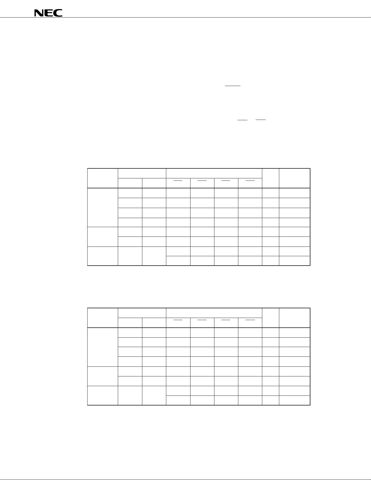
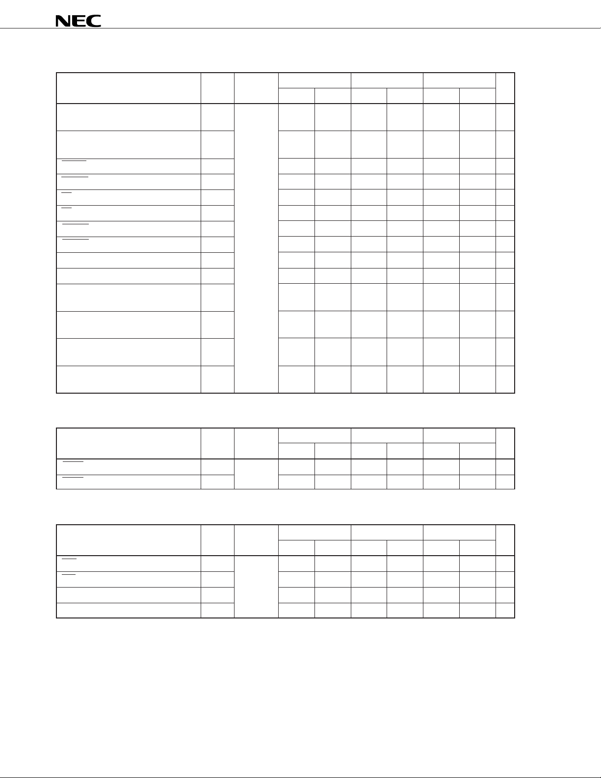
1. PIN FUNCTIONS
1.1 Pin Function List
µPD70732
Bus hold
Name I/O Function status status
A31 to A1 3-state Address bus Hi-Z Hi-Z H
(Address Bus) output
D31 to D0 3-state Bidirectional data bus Hi-Z Hi-Z Hi-Z
(Data Bus) I/O
BE3 to BE0 3-state Indicates valid data bus when data is accessed Hi-Z Hi-Z H
(Byte Enable) output
ST1, ST0 3-state Indicates type of bus cycle Hi-Z Hi-Z H
(Status) output
DA 3-state Strobe signal for bus cycle Hi-Z Hi-Z H
(Data Access) output
MRQ 3-state Indicates memory access Hi-Z Hi-Z H
(Memory Request) output
R/W 3-state Distinguishes between read access and write access Hi-Z Hi-Z H
(Read/Write) output
BCYST 3-state Indicates start of bus cycle Hi-Z Hi-Z H
(Bus Cycle Start) output
status
during
operation
Bus hold Bus idle
at reset at reset
Note
READY Input Extends bus cycle — — —
(Ready)
HLDRQ Input Requests bus mastership — — —
(Hold Request)
HLDAK Output Acknowledges HLDRQ L L H
(Hold Acknowledge)
SZRQ Input Requests bus sizing — — —
(Bus Sizing Request)
SIZ16B Input Fixes external data bus width to 16 bits — — —
(Bus Size 16 Bit)
BLOCK Output Requests to inhibit use of bus L L L
(Bus Lock)
ICHEEN Input Operates instruction cache — — —
(Instruction Cache Enable)
INT Input Interrupt request — — —
(Maskable Interrupt)
INTV3 to INTV0 Input Interrupt level — — —
(Interrupt Level)
Note A1 pin is “H” in the 16-bit bus fixed mode; otherwise, it is “L”.
8

µPD70732
Bus hold
Name I/O Function status status
NMI Input Non-maskable interrupt request — — —
(Non-Maskable Interrupt)
CLK Input CPU clock input — — —
RESET Input Resets internal status — — —
(Reset)
ADRSERR Output Indicates that data alignment is illegal Not H H
(Address Error) affected
DD — Positive power supply — — —
V
(Power Supply)
GND — Ground potential (0 V) — — —
(Ground)
IC1 — Internally connected (Leave this pin open.) — — —
(Internally Connected 1)
IC2 — Internally connected (Ground this pin.) — — —
(Internally Connected 2)
status
during
operation
Bus hold Bus idle
at reset at reset
IC3 — Internally connected (Connect this pin to power supply.) — — —
(Internally Connected 3)
9

★
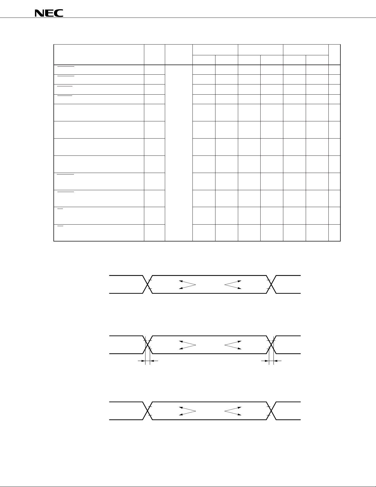
1.2 Pin I/O Circuits and Recommended Connection of Unused Pins
The I/O circuit type of each pin and recommended connection of unused pins are shown in Table 1-1. Figure
1-1 shows the I/O circuit of each type.
Table 1-1. Pin I/O Circuit Types and Recommended Connection Method of Unused Pins
Pin I/O Circuit Type Recommended Connection Method
D31 to D0 5 Open
A31 to A1 4
BE3 to BE0
ST1, ST0
DA
MRQ
R/W
BCYST
READY 1 Connect to GND via resistor
HLDRQ Connect to VDD via resistor
HLDAK 4 Open
SZRQ 1 Connect to VDD via resistor
SIZ16B Connect to GND via resistor
BLOCK 4 Open
ICHEEN 1 Connect to VDD via resistor
INT Connect to GND via resistor
INTV3 to INTV0 Connect to VDD via resistor
NMI
CLK —
RESET
ADRSERR 4 Open
IC1 —
IC2 — Connect to GND
IC3 — Connect to VDD
µPD70732
10

Figure 1-1. Pin I/O Circuit
µPD70732
Type 1
V
DD
P-ch
IN
N-ch
Type 4
V
DD
data
output
disable
Push-pull output that can be output high impedance
(both P-ch and N-ch are off).
P-ch
N-ch
OUT
Type 5
output
disable
enable
data
input
V
DD
P-ch
N-ch
IN/OUT
11

★
2. REGISTER SET
The registers of the V810 can be classified into two types: general-purpose program register set and dedicated
system register set. All registers are 32 bits wide.
Program register sets System register sets
31 0 31 0
r0 Zero Register EIPC Exception/Interrupt PC
r1 Reserved for Address Generation EIPSW Exception/Interrupt PSW
r2 Handler Stack Pointer (hp)
r3 Stack Pointer (sp) 31 0
r4 Global Pointer (gp) FEPC Fatal Error PC
r5 Text Pointer (tp) FEPSW Fatal Error PSW
r6
r7 31 0
r8 ECR Exception Cause Register
r9
r10 31 0
r11 PSW Program Status Word
r12
r13 31 0
r14 PIR Processor ID Register
r15
r16 31 0
r17 TKCW Task Control Word
r18
r19 31 0
r20 CHCW Cache Control Word
r21
r22 31 0
r23 ADTRE Address Trap Register
r24
r25
r26 String Destination Bit Offset
r27 String Source Bit Offset
r28 String Length
r29 String Destination
r30 String Source
r31 Link Pointer (lp)
µPD70732
12
31 0
PC Program Counter

µPD70732
2.1 Program Register Set
The program register set is composed of general-purpose registers and a program counter.
(1) General-purpose registers
Thirty-two general-purpose registers, r0 to r31, are available. All these registers can be used as data
registers or address registers.
Of these registers, r0 and r26 through r30 are implicitly used by some instructions, and r1 through r5 and
r31 are implicitly used by the assembler and C compiler. Therefore, when using these registers, it is
necessary to take special care such as saving these registers’ contents to different areas before using
these registers and restoring the contents after using them.
Table 2-1. Program Registers
Register Application Operation
r0 Zero register Always holds zeros.
r1 Register reserved for assembler Used as a working register to generate a 32-bit immediate data.
r2 Handler stack pointer Used as the stack pointer for the handler.
r3 Stack pointer Used to generate a stack frame at a function call.
r4 Global pointer Used to access a global variable in the data area.
r5 Text pointer Points the start address of the text area.
r6 to r25 — Stores address or data variables.
r26 String destination bit offset Used in a bit-string instruction execution.
r27 String source bit offset
r28 String length register
r29 String destination address register
r30 String address register
r31 Link pointer Stores the return address at execution of a JAL instruction.
(2) Program Counter
The program counter (PC) indicates the address of the instruction currently executed by the program.
Bit 0 of the PC is fixed to 0, and execution cannot branch to an odd address. The contents of the PC
are initialized to FFFFFFF0H at reset.
13

µPD70732
2.2 System Register Set
The system register set is composed of the following registers that perform operations such as CPU-status
control and interrupt information holding.
Table 2-2. System Register Number
Number Register Name Application Operation
0 EIPC Status saving registers The EIPC and EIPSW registers save the PC and PSW,
for exception/interrupt respectively, when an exception or interrupt occurs. Because in
the V810 the registers incorporated for this purpose are
1 EIPSW these registers only, save the contents of these registers by means
of programming if your application set can cause multiple interrupt
requests to be issued in the V810.
2 FEPC Status saving registers for The FEPC and FEPSW registers save the PC and PSW,
3 FEPSW
4 ECR Exception cause register This register, when an exception, maskable interrupt, or NMI
5 PSW Program status word This register, also called the program status word, is a set of flags
6 PIR Processor ID register This register identifies the CPU type number.
7 TKCW Task control word This register controls floating-point operations.
8 to 23 Reserved
24 CHCW Cache control word This register controls the on-chip instruction cache.
25 ADTRE Address trap register This register holds an address and is used for address trapping.
26 to 31 Reserved
NMI/duplexed exception respectively, when an NMI or duplexed exception occurs.
occurs, holds its cause. This register consists of 32 bits. Its higher
16 bits, called FECC, hold the exception code for an NMI or
duplexed exception, while the lower 16 bits, called EICC, hold the
exception code for an exception or maskable interrupt.
indicating the statuses of the CPU and program (instruction execution
results).
When the address in this register matches the PC value, the
execution jumps to a predefined address.
To read or write one of the registers shown above, specify a system register number with the system register
load (LDSR) or system register store (STSR) instruction.
14

µPD70732
3. DATA TYPES
3.1 Data Types
The data types supported by the V810 are as follows:
• Integer (8, 16, 32 bits)
• Unsigned integer (8, 16, 32 bits)
• Bit string
• Single-precision floating-point data (32 bits)
3.1.1 Data type and addressing
The V810 uses the little-endian data addressing. In this addressing, if a fixed-length data is located in a memory
area, the data must be either of the data types shown below.
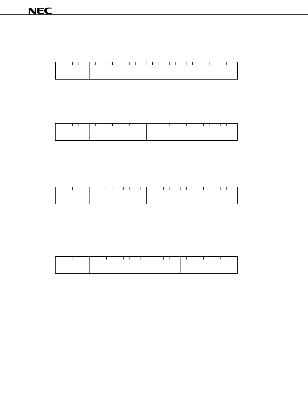
(1) Byte
A byte is a consecutive 8-bit data whose first-bit address is aligned to a byte boundary. Each bit in a
byte is numbered from 0 to 7: LSB (the least significant bit) is bit 0 and MSB (the most significant bit)
is bit 7. To access a byte, specify address A. (See diagram below.)
70
A
★
(2) Halfword
A halfword is a consecutive 16-bit (= 2 bytes) data whose first-bit address is aligned to a halfword
boundary. Each bit in a halfword is numbered from 0 to 15: LSB (the least significant bit) is bit 0 and
MSB (the most significant bit) is bit 15. To access a halfword, specify the address A only (lowest bit must
be 0).
15 8 7
A + 1
0
A
(3) Word/short real
A word, also called short real, is a consecutive 32-bit (= 4 bytes) data whose first-bit address is aligned
to a word boundary. Each bit in a word is numbered from 0 to 31: LSB (the least significant bit) is bit
0 and MSB (the most significant bit) is bit 31. To access a word or short real, specify the address A only
(lower two bits must be 0).
31 24 23
A + 3
16 15
A + 2
A + 1
87
0
A
15

µPD70732
3.1.2 Integer
In the V810, all integers are expressed in the two’s-complement binary notation, and are composed of either
8 bits, 16 bits, or 32 bits. Regardless of the data length, bit 0 is the least significant bit, and higher-numbered
bits express higher digits of the integer with the highest bit expressing its sign.
Data Length Range
Byte 8 bits –128 to +127
Halfword 16 bits –32768 to +32767
Word 32 bits –2147483648 to +2147483647
3.1.3 Unsigned integer
An unsigned integer is either zero or a positive integer unlike the integer explained in section 3.1.2 which can
be negative as well as zero and positive. Unsigned integers are expressed in the binary notation in the same way
as integers, and are either 8 bits, 16 bits, or 32 bits long. Regardless of the data length, the bit assignments are
the same as in the case of integers except that unsigned integers do not include a sign bit; the highest bit is also
a part of the integer.
Data Length Range
Byte 8 bits 0 to 255
Halfword 16 bits 0 to 65535
Word 32 bits 0 to 4294967295
3.1.4 Bit string
32
A bit string is a type of data whose bit length is variable from 0 to 2
– 1. To specify a bit-string data, define
the following three attributes.
• A : address of the string data’s first word (lower two bits must be 0.)
• B : in-word bit offset in the string data (0 to 31)
• M: bit length of the string data (0 to 2
32
– 1)
The above three attributes may vary depending on the bit-string data manipulation direction: upward or
downward, as shown below. The former is the direction from lower addresses to higher addresses while the latter
is the direction from higher to lower addresses.
M– 1 0
M
A + 8
D
Attribute Upward Downward
First-word address (0s in bits 1 and 0) A A + 4
In-word bit offset (0 to 31) B D
Bit length (0 to 2
32
– 1) M M
A + 4 A (Word boundary)
B
16

µPD70732
3.1.5 Single-precision floating-point data
This data type is 32 bits long and its bit allocation complies with the IEEE single format. A single-precision
floating-point data consists of 1-bit mantissa sign bit, 8-bit exponent, and 23-bit mantissa. The exponent is offsetexpressed from the bias value – 127, and the mantissa is binary-expressed with the integer part omitted.
31 2330
s exp (8) mantissa (23)
3.2 Data Alignment
In the V810, a word data must be aligned to a word boundary (with the lowest two bits of the address fixed
to 0s), and a halfword data to a halfword boundary (with the lowest bit of the address fixed to 0). If a data is not
aligned as specified, the lowest one bit (in the case of word) or two bits (in the case of halfword) of its address
will forcibly be masked with 0s when the data is accessed.
22 0
17

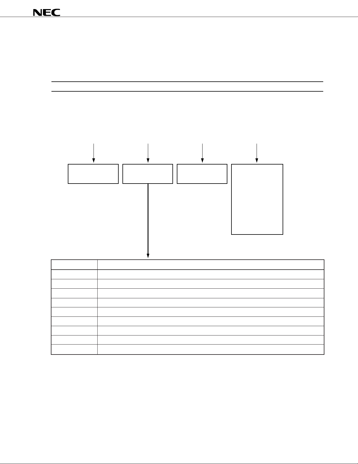
4. ADDRESS SPACE
★
The V810 supports 4 Gbytes of linear memory space and I/O space. The CPU outputs 32-bit addresses to
32
the memory and I/Os; therefore, the addresses are from 0 to 2
– 1.
Bit number 0 of each byte data is defined as the LSB (Least Significant Bit), and bit number 7 is the MSB (Most
Significant Bit). Unless otherwise specified, the byte data at the lower address side of data consisting of two or
more bytes is the LSB, and the byte data at the higher address side is the MSB (little endian).
Data consisting of 2 bytes is called a halfword, and data consisting of 4 bytes is called a word. The lower address
of memory or I/O data of two or more bytes, here, is shown on the right, and the higher address is shown on the
left, as follows:
µPD70732
Byte of address A
Halfword of address A
Word/short real of address A
70
A (address)
7015 8
A (address)A + 1
7015 823 1631 24
AA + 1A + 2A + 3
18

Figure 4-1 shows the memory map of the V810, and Figure 4-2 shows the I/O map.
Figure 4-1. Memory Map
FFFFFFFFH
µPD70732
FFFFFE00H
FFFFFDFFH
Interrupt handler table
General use
Note
00000000H
Note For the details, refer to Table 6-1 Exception Codes.
19

FFFFFFFFH
µPD70732
Figure 4-2. I/O Map
General use
00000000H
20
µPD70732
5. BUS INTERFACE FUNCTION
The V810 is equipped with a 32-bit data bus.
In the bus interface, there are two modes: 32-bit bus mode which uses the data bus in 32 bits and 16-bit bus
fixed mode which fixes the bus in 16 bits. Modes can be switched only at reset using the SIZ16B signal.
The 32-bit bus mode has a dynamic bus sizing function which uses the data bus in 16-bit bus width to access
the 16-bit peripherals. This function can be used by setting the SZRQ signal active. Access to word data
(32-bit data) in the dynamic bus sizing is executed by loading/storing a 16-bit data twice.
In the 16-bit bus fixed mode, access to word data (32-bit data) is executed by activating a bus cycle twice.
The control signal and the A1 signal output values according to the 16-bit system.
The relationship between the external access and byte enable signals (BE3 to BE0) during the 32-bit bus mode
and the 16-bit bus fixed mode is shown below.
Table 5-1. Relationship among Address, Data Length, Byte Enable Signals and A1
(32-bit bus mode)
Data length
Operand address Byte enable
Bit 1 Bit 0 BE3 BE2 BE1 BE0
Byte 0 0 1 1 1 0 0 1
01110101
10101101
11011101
Halfword 0 0 1 1 0 0 0 1
10001101
Word 0 0 0 0 0 0 0 1
001112
A1
Bus cycle
sequence
Note
★
Note Bus cycle added by dynamic bus sizing
Table 5-2. Relationship among Address, Data Length, Byte Enable Signals and A1
(16-bit bus fixed mode)
Data length
Byte 0 0 Hi-Z Hi-Z 1 0 0 1
Halfword 0 0 Hi-Z Hi-Z 0 0 0 1
Word 0 0 Hi-Z Hi-Z 0 0 0 1
Operand address Byte enable
Bit 1 Bit 0 BE3 BE2 BE1 BE0
0 1 Hi-Z Hi-Z 0 1 0 1
1 0 Hi-Z Hi-Z 1 0 1 1
1 1 Hi-Z Hi-Z 0 1 1 1
1 0 Hi-Z Hi-Z 0 0 1 1
Hi-Z Hi-Z 0 0 1 2
A1
Bus cycle
sequence
Note
Note Added bus cycle
21

6. INTERRUPT AND EXCEPTION
★
Interrupts are events that take place independently of the program execution and can be classified into
maskable interrupts and a non-maskable interrupt. An exception is an event that takes place depending upon the
program execution. There is little difference between the interrupt and exception in terms of flow, but the interrupt
takes precedence over the exception.
The V810 architecture is provided with the interrupts and exceptions listed in the table below. If an exception,
a maskable interrupt or NMI occurs, control is transferred to a handler whose address is determined by the source
of the interrupt or exception. The exception source can be checked by examining an exception code stored in the
ECR (Exception Code Register). Each handler analyzes the contents of the ECR and performs appropriate
exception/interrupt servicing.
Table 6-1. Exception Codes
µPD70732
Exception and interrupt Classification Exception code Handler address Restore PC
Reset Interrupt F F F 0 F F F F F F F 0 Note 2
NMI Interrupt F F D 0 F F F F F F D 0 next PC
Duplexed exception Exception Note 4 F F F F F F D 0 current PC
Address trap Exception F F C 0 F F F F F F C 0 current PC
Trap instruction (parameter is 0x1n) Exception F F B n F F F F F F B 0 next PC
Trap instruction (parameter is 0x0n) Exception F F A n F F F F F F A 0 next PC
Invalid instruction code Exception F F 9 0 F F F F F F 9 0 current PC
Zero division Exception F F 8 0 F F F F F F 8 0 current PC
FIV (floating-point invalid operation) Exception F F 7 0 F F F F F F 6 0 current PC
FZD (floating-point zero division) Exception F F 6 8 F F F F F F 6 0 current PC
FOV (floating-point overflow) Exception F F 6 4 F F F F F F 6 0 current PC
FUD (floating-point underflow)
FPR (floating-point precision degradation)
FRO (floating-point reserved operand) Exception F F 6 0 F F F F F F 6 0 current PC
INT level n (n = 0 to 15) Interrupt F E n 0 F F F F F E n 0 next PC
Note 5
Note 5
Exception F F 6 2 F F F F F F 6 0 current PC
Exception F F 6 1 F F F F F F 6 0 current PC
Note 3
Note 3
Notes 1. PC to be saved to EIPC or FEPC.
2. EIPC and FEPC are undefined.
3. While an instruction whose execution is aborted by an interrupt (DIV/DIVU, single-precision floating-
point data, bit string instruction) is executed, restore PC = current PC.
4. The exception code of the exception that occurs for the first time is stored to the lower 16 bits of
the ECR, and that of the second exception is stored in the higher 16 bits.
5. In the V810, the floating-point underflow exception and floating-point precision degradation exception
do not occur.
Note 1
22

µPD70732
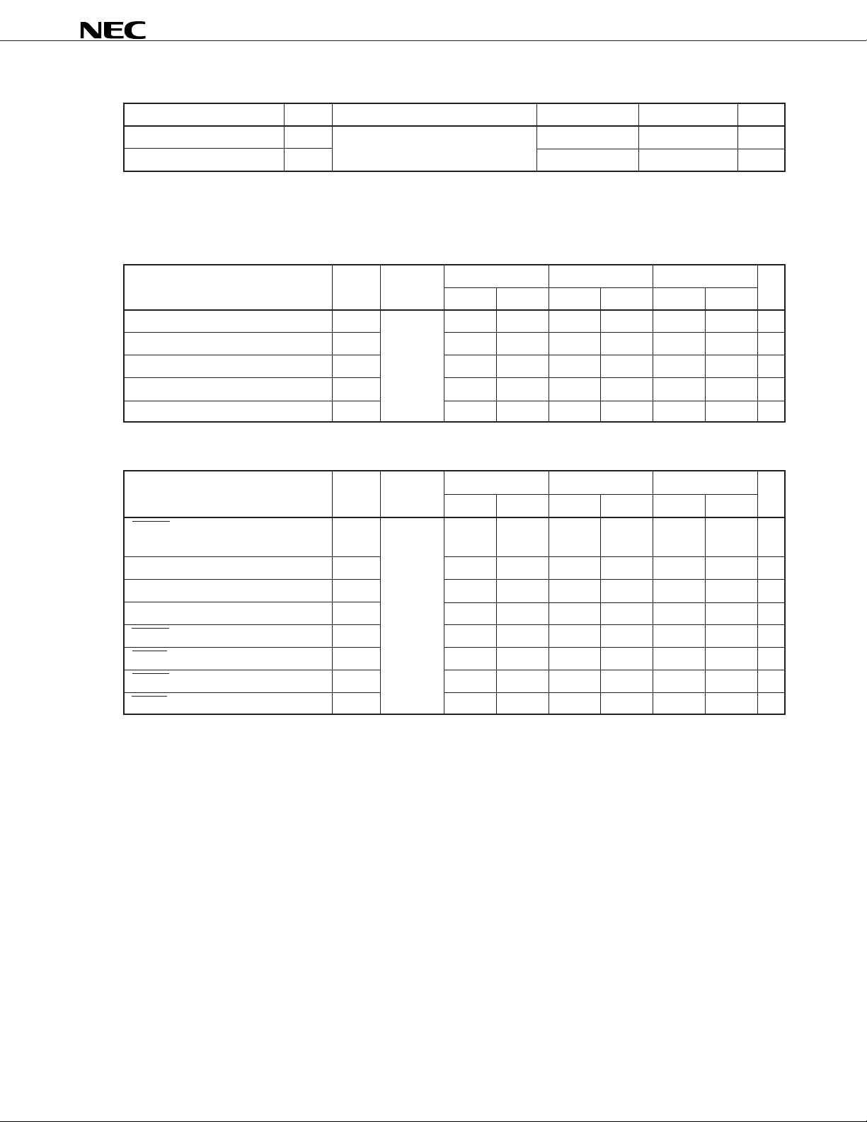
7. CACHE
Figure 7-1 shows the instruction cache configuration provided to the V810.
Figure 7-1. Cache Configuration
Capacity : 1 Kbytes
Mapping system : direct map
Block size : 8 bytes
Sub-block size : 4 bytes
31
Memory address TAG
Tag memory
(ICHT27 to ICHT0)
27 22 31 0021
Entry 0
TAG31 to TAG10
Sub-block (4 bytes)
9320
10
OffsetIndex
Data memory
(ICHD31 to ICHD0)
Block
(8 bytes)
★
128 entries
Entry 127
Entry 1
128 blocks
Valid bits (1 bit for every 4 bytes)
NECRV (Reserved by NEC)
23

8. RESET
★
A low-level input detection on the RESET pin always triggers a system reset. Consequently, all the hardwarecontrolling registers are initialized as shown in Table 8-1. After the initialization procedure is completed and the
RESET pin returns to the high level, the device is released from the resetting state and starts the implementation
of a program. Then, if necessary, set some registers to user-desired values in the first stage of the program.
Table 8-1. Register State after Reset
Hardware (Symbol) State after Reset
Program counter PC FFFFFFF0H
Status saving register for interrupt EIPC Undefind
EIPSW
Status saving register for NMI FEPC Undefind
FEPSW
Interrupt cause register FECC 0000H
EICC FFF0H
Program status word PSW 00008000H
General-purpose register r0 Fixed to 00000000H
r1 to r31 Undefind
µPD70732
24

µPD70732
9. INSTRUCTION SET
9.1 Instruction Format
The V810 instructions are formatted in either 16 bits or 32 bits. Examples of the 16-bit format instruction are
binomial operation, control, and conditional branch; those for the 32-bit format are load/store, I/O manipulate, 16bit immediate, jump & link, and extended operations.
Some instructions have an unused field. However, do not write a program that uses this field because it is
reserved for future use. This unused field must be set to zeros.
Instructions are stored in memory in the following manner.
• The lower half of an instruction, that is, the half which includes bit 0, is stored at the lower address.
• The higher half of an instruction, that is, the half which includes bit 15 or 31, is stored at the higher address.
(1) reg-reg instruction format (Format I)
This format consists of one 6-bit field to hold an operation code and two 5-bit fields to specify generalpurpose registers as instruction’s operands. 16-bit instructions use this format.
15 10
opcode reg2 reg1
9540
★
(2) imm-reg instruction format (Format II)
This format consists of one 6-bit field to hold an operation code, one 5-bit field to hold an immediate data,
and one field to specify a general-purpose register as an operand. 16-bit instructions use this format.
15 10
opcode reg2 imm
9540
(3) Conditonal branch instruction format (Format III)
This format consists of one 3-bit field to hold an operation code, one 4-bit field to hold a condition code,
and one 9-bit field to hold a branch displacement (with its LSB masked to 0). 16-bit instructions use this
format.
15 13
opcode cond disp
12 9 8 0
0
25
(4) Intermediate jump instruction format (Format IV)
This format consists of one 6-bit field to hold an operation code and one 26-bit field to hold a displacement
(with its LSB masked to 0). 32-bit instructions use this format.
µPD70732
15 10
opcode disp
9 0 31 16
0
(5) 3-operand instruction format (Format V)
This format consists of one 6-bit field to hold an operation code, two fields to specify general-purpose
registers as operands, and one 16-bit field to hold an immediate data. 32-bit instructions use this format.
15 10
opcode reg2 reg1 imm
9 5 4 0 31 16
(6) Load/store instruction format (Format VI)
This format consists of one 6-bit field to hold an operation code, two fields to specify a general-purpose
register, and one 16-bit field to hold a displacement. 32-bit instructions use this format.
15 10
opcode reg2 reg1 disp
9 5 4 0 31 16
(7) Extension instruction format (Format VII)
This format consists of one 6-bit field to hold an operation code, two 5-bit fields to specify general-purpose
registers as operands, and one 6-bit field to hold an sub-operation code. The remaining 10 bits are
reserved for future use and must be set to zeros. 32-bit instructions use this format.
15 10
opcode reg2 reg1 sub-opcode RFU
9 5 4 0 31 16
26
µPD70732
9.2 Instruction Mnemonic (in alphabetical order)
The list of mnemonics is shown below.
This section lists the instructions incorporated in the V810 along with their operations. The instructions are
listed in the instruction mnemonic’s alphabetical order to allow users to use this section as a quick reference or
dictionary. The conventions used in the list are shown below.
Legend
Instruction Mnemonic
ADD
Mnemonic of instruction
Operand (s) Format Instruction FunctionCY OV S Z
reg1, reg2
Identifier of operand
I
Instruction format
(Refer to 9.1.)
****
Flag operation
Remains unchanged
–
Inverts the previous value
*
Changes to 0
0
Changes to 1
1
Identifier Description
reg1 General-purpose register (Used as a source register)
reg2 General-purpose register (Used mainly as a destination register and occasionally as a source register)
imm5 5-bit immediate
imm16 16-bit immediate
disp9 9-bit displacement
disp16 16-bit displacement
disp26 26-bit displacement
regID System register number
vector adr Trap handler address that corresponds to a trap vector
27

µPD70732
Table 9-1. Instruction Mnemonics (in alphabetical order) (1/9)
Instruction Operand (s) Format CY OV S Z Instruction Function
Mnemonic
ADD reg1, reg2 I * * * * Addition:
Adds the word data in the reg2-specified register and
the word data in the reg1-specified register, then
stores the result into the reg2-specified register.
ADD imm5, reg2 II * * * * Addition:
Sign-extends the 5-bit immediate data to 32 bits, and
adds the extended immediate data and the word data
in the reg2-specified register, then stores the result
into the reg2-specified register.
ADDF.S reg1, reg2 VII * 0 * * Floating-point addition:
Adds the single-precision floating-point data in the
reg2-specified register and the single-precision floatingpoint data in the reg1-specified register, then restores
the result into the reg2-specified register while changing
flags according to the result.
ADDI imm16, reg1, reg2 V * * * * Addition:
Sign-extends the 16-bit immediate data to 32 bits, and
adds the extended immediate data and the word data
in the reg1-specified register, then stores the result
into the reg2-specified register.
AND reg1, reg2 I – 0 * * AND:
Performs the logical AND operation on the word data
in the reg2-specified register and the word data in the
reg1-specified register, then stores the result into the
reg2-specified register.
ANDBSU – II – – – – Transfer after ANDing bit strings:
Performs a logical AND operation on a source bit
string and a destination bit string, then transfers the
result to the destination bit string.
ANDI imm16, reg1, reg2 V – 0 0 * AND:
Sign-extends the 16-bit immediate data to 32 bits, and
performs a logical AND operation on the extended
immediate data and the word data in the reg1-specified
register, then stores the result into the reg2-specified
register.
ANDNBSU – II – – – – Transfer after NOTting a bit string then ANDing it with
another bit string:
Performs a logical AND operation on a destination bit
string and the 1’s complement of a source bit string,
then transfers the result to the destination bit string.
BC disp9 III – – – – Conditional branch (if Carry):
PC relative branch
BE disp9 III – – – – Conditional branch (if Equal):
PC relative branch
BGE disp9 III – – – – Conditional branch (if Greater than or Equal):
PC relative branch
BGT disp9 III – – – – Conditional branch (if Greater than):
PC relative branch
28

µPD70732
Table 9-1. Instruction Mnemonics (in alphabetical order) (2/9)
Instruction Operand (s) Format CY OV S Z Instruction Function
Mnemonic
BH disp9 III – – – – Conditional branch (if Higher):
PC relative branch
BL disp9 III – – – – Conditional branch (if Lower):
PC relative branch
BLE disp9 III – – – – Conditional branch (if Less than or Equal):
PC relative branch
BLT disp9 III – – – – Conditional branch (if Less than):
PC relative branch
BN disp9 III – – – – Conditional branch (if Negative):
PC relative branch
BNC disp9 III – – – – Conditional branch (if Not Carry):
PC relative branch
BNE disp9 III – – – – Conditional branch (if Not Equal):
PC relative branch
BNH disp9 III – – – – Conditional branch (if Not Higher):
PC relative branch
BNL disp9 III – – – – Conditional branch (if Not Lower):
PC relative branch
BNV disp9 III – – – – Conditional branch (if Not Overflow):
PC relative branch
BNZ disp9 III – – – – Conditional branch (if Not Zero):
PC relative branch
BP disp9 III – – – – Conditional branch (if Positive):
PC relative branch
BR disp9 III – – – – Unconditional branch:
PC relative branch
BV disp9 III – – – – Conditional branch (if Overflow):
PC relative branch
BZ disp9 III – – – – Conditional branch (if Zero):
PC relative branch
CAXI disp16 [reg1], reg2 VI * * * * Inter-processor synchronization in a multi-processor
system.
CMP reg1, reg2 I * * * * Comparison:
Subtracts the word data in the reg1-specified register
from that for reg2 for comparison, then changes flags
according to the result.
CMP imm5, reg2 II * * * * Comparison:
Sign-extends the 5-bit immediate data to 32 bits, and
subtracts the extended immediate data from the word
data in the reg2-specified register for comparison,
then changes flags according to the result.
CMPF.S reg1, reg2 VII * 0 * * Floating-point comparison:
Subtracts the single-precision floating-point data in
the reg1-specified register from that for reg2 for
comparison, then changes flags according to the
result.
29

µPD70732
Table 9-1. Instruction Mnemonics (in alphabetical order) (3/9)
Instruction Operand (s) Format CY OV S Z Instruction Function
Mnemonic
CVT.SW reg1, reg2 VII – 0 * * Data conversion from floating-point to integer:
Converts the single-precision floating-point data in the
reg1-specified register into an integer data, then stores
the result into the reg2-specified register while changing
flags according to the result.
CVT.WS reg1, reg2 VII * 0 * * Data conversion from integer to floating-point:
Converts the integer data in the reg1-specified register
into a single-precision floating-point data, then stores
the result into the reg2-specified register while changing
flags according to the result.
DIV reg1, reg2 I – * * * Signed division:
Divides the word data in the reg2-specified register by
that for reg1 with their sign bits validated, then stores
the quotient into the reg2-specified register and the
remainder into r30. Division is performed so that the
sign of the remainder matches that of the dividend.
DIVF.S reg1, reg2 VII * 0 * * Floating-point division:
Divides the single-precision floating-point data in the
reg2-specified register by that for reg1, then stores the
result into the reg2-specified register while changing
flags according to the result.
DIVU reg1, reg2 I – 0 * * Unsigned division:
Divides the word data in the reg2-specified register by
that for reg1 with their data handled as unsigned data,
then stores the quotient into the reg2-specified register
and the remainder into r30. Division is performed so
that the sign of the remainder matches that of the
dividend.
HALT – II – – – – Processor stop
IN.B disp16 [reg1], reg2 VI – – – – Port input:
Sign-extends the 16-bit displacement to 32 bits, and
adds the extended displacement and the content of
the reg1-specified register to generate a 32-bit unsigned
port address, then reads the byte data located at the
generated port address, zero-extends the byte data to
32 bits, and stores the result into the reg2-specified
register.
IN.H disp16 [reg1], reg2 VI – – – – Port input:
Sign-extends the 16-bit displacement to 32 bits, and
adds the extended displacement and the content of
the reg1-specified register to generate a 32-bit unsigned
port address, then reads the halfword data located at
the generated port address while masking the address’s
bit 0 to 0, zero-extends the halfword data to 32 bits,
and stores the result into the reg2-specified register.
30

µPD70732
Table 9-1. Instruction Mnemonics (in alphabetical order) (4/9)
Instruction Operand (s) Format CY OV S Z Instruction Function
Mnemonic
IN.W disp16 [reg1], reg2 VI – – – – Port input:
Sign-extends the 16-bit displacement to 32 bits, and
adds the extended displacement and the content of
the reg1-specified register to generate a 32-bit unsigned
port address, then reads the word data located at the
generated address while masking the address’s bits
0 and 1 to 0, and stores the word into the reg2specified register.
JAL disp26 IV – – – – Jump and link:
Increments the current PC by 4, then saves it into r31,
and sign-extends the 26-bit displacement to 32 bits
while masking the displacement’s bit 0 to 0, adds the
extended displacement and the PC value, loads the
PC with the addition result, so that the instruction
stored at the PC-pointing address is executed next.
JMP [reg1] I – – – – Register-indirect unconditional branch:
Loads the PC with the jump address value in the reg1specified register while masking the value’s bit 0 to 0,
so that the instruction stored at the address pointed
by the reg1-specified register is executed next.
JR disp26 IV – – – – Unconditional branch:
Sign-extends the 26-bit displacement to 32 bits while
masking bit 0 to 0, adds the result with the current PC
value, and loads the PC with the addition result so that
the instruction stored at the PC-pointing address is
executed next.
LD.B disp16 [reg1], reg2 VI – – – – Byte load:
Sign-extends the 16-bit displacement to 32 bits, and
adds the result with the content of the reg1-specified
register to generate the 32-bit unsigned address, then
reads the byte data located at the generated address,
sign-extends the byte data to 32 bits, and stores the
result into the reg2-specified register.
LD.H disp16 [reg1], reg2 VI – – – – Halfword load:
Sign-extends the 16-bit displacement to 32 bits, and
adds the result with the content of the reg1-specified
register to generate a 32-bit unsigned address while
masking its bit 0 to 0, then reads the halfword data
located at the generated address, sign-extends the
halfword data to 32 bits, and stores the result into the
reg2-specified register.
LD.W disp16 [reg1], reg2 VI – – – – Word load:
Sign-extends the 16-bit displacement to 32 bits and
adds the result with the content of the reg1-specified
register to generate a 32-bit unsigned address while
masking bits 0 and 1 to 0, then reads the word data
located at the generated address and stores the data
into the reg2-specified register.
31

Table 9-1. Instruction Mnemonics (in alphabetical order) (5/9)
Instruction Operand (s) Format CY OV S Z Instruction Function
Mnemonic
LDSR reg2, regID II * * * * Loading system register:
Transfers the word data in the reg2-specified register
to the system register specified with the system register
number (regID).
MOV reg1, reg2 I – – – – Transferring data:
Loads the reg2-specified register with the word data
in of the reg1-specified register.
MOV imm5, reg2 II – – – – Transferring data:
Sign-extends the 5-bit immediate data to 32 bits, then
loads the reg2-specified register with the extended
immediate data.
MOVBSU – II – – – – Transferring bit strings:
Loads the destination bit string with the source bit
string.
MOVEA imm16, reg1, reg2 V – – – – Addition:
Sign-extends the 16-bit immediate data to 32 bits,
adds it with the word data in the reg1-specified register,
then stores the addition result into reg2.
MOVHI imm16, reg1, reg2 V – – – – Addition:
Appends 16-bit zeros below the 16-bit immediate data
to form a 32-bit word data, then adds it with the word
data in the reg1-specified register, and stores the
result into the reg2-specified register.
MUL reg1, reg2 I – * * * Signed multiplication:
Signed-multiplies the word data in the reg2-specified
register by that for reg1, then separates the 64-bit
(double-word) result into two 32-bit data, and stores
the higher 32 bits into r30 and the lower 32 bits into
the reg2-specified register.
MULF.S reg1, reg2 VII * 0 * * Floating-point multiplication:
Multiplies the single-precision floating-point data in
the reg2-specified register by that for reg1, then stores
the result into the reg2-specified register while changing
flags according to the result.
MULU reg1, reg2 I – * * * Unsigned multiplication:
Multiplies the word data in the reg2-specified register
by that for reg1 while handling these data as unsigned
data, then separates the 64-bit (double-word) result
into two 32-bit data, and stores the higher 32 bits into
r30 and the lower 32 bits into the reg2-specified
register.
NOP – III – – – – No operation:
Makes no changes or operations while spending one
instruction cycle.
NOT reg1, reg2 I – 0 * * Logical NOT:
Obtains the 1’s complement (logical NOT) of the
content of the reg1-specified register, then stores the
result into the reg2-specified register.
µPD70732
32

µPD70732
Table 9-1. Instruction Mnemonics (in alphabetical order) (6/9)
Instruction Operand (s) Format CY OV S Z Instruction Function
Mnemonic
NOTBSU – II – – – – Transfer after NOTting a bit string:
Obtains the 1’s complement (all bits inverted) of the
source bit string, then transfers the result to the
destination bit string.
OR reg1, reg2 I – 0 * * OR:
Performs a logical OR operation on the word data in
the reg2-specified register and that for reg1, then
stores the result into the reg2-specified register.
ORBSU – II – – – – Transfer after ORing bit strings:
Performs a logical OR operation on the source and
destination bit strings, then transfers the result to the
destination bit string.
ORI imm16, reg1, reg2 V – 0 * * OR:
Zero-extends the 16-bit immediate data to 32 bits,
performs a logical OR operation on the extended data
and the word data in the reg1-specified register, then
stores the result into the reg2-specified register.
ORNBSU – II – – – – Transfer after NOTting a bit string and ORing it with
another bit string:
Obtains the 1’s complement (logical NOT) of the
source bit string, performs a logical OR operation on
the NOTted bit string and the destination bit string,
then transfers the result to the destination bit string.
OUT.B reg2, disp16 [reg1] VI – – – – Port output:
Sign-extends the 16-bit displacement to 32 bits, adds
the extended value and the content of the reg1specified register to generate a 32-bit unsigned port
address, then outputs the lowest 8 bits (= 1 byte) of
the reg2-specified register onto the port pins
corresponding to the generated port address.
OUT.H reg2, disp16 [reg1] VI – – – – Port output:
Sign-extends the 16-bit displacement to 32 bits, adds
the extended value and the content of the reg1specified register to generate a 32-bit unsigned port
address with its bit 0 masked to 0, then outputs the
lowest 16 bits (= 1 halfword) of the reg2-specified
register onto the port pins corresponding to the generated
port address.
OUT.W reg2, disp16 [reg1] VI – – – – Port output:
Sign-extends the 16-bit displacement to 32 bits, adds
the extended value and the content of the reg1specified register to generate a 32-bit unsigned port
address with its bits 0 and 1 masked to 0, then outputs
the 32 bits (= 1 word) of the reg2-specified register
onto the port pins corresponding to the generated port
address.
33

µPD70732
Table 9-1. Instruction Mnemonics (in alphabetical order) (7/9)
Instruction Operand (s) Format CY OV S Z Instruction Function
Mnemonic
RETI – II * * * * Return from a trap or interrupt routine:
Reads the restore PC and PSW from the system
registers and loads them to the due places to return
from a trap or interrupt routine to the original operation
flow.
SAR reg1, reg2 I * 0 * * Arithmetic right shift:
Shifts every bit of the word data in the reg2-specified
register to the right by the number of times specified
with the reg1-specified register’s lowest 5 bits, then
stores the result into the reg2-specified register. In
arithmetic right shift operations, the MSB is loaded
with the LSB value at each shift.
SAR imm5, reg2 II * 0 * * Arithmetic right shift:
Zero-extends the 5-bit immediate data to 32 bits, shifts
every bit of the word data in the reg2-specified register
to the right by the number of times specified with the
extended immediate data, then stores the result into
the reg2-specified register. In arithmetic right shift
operations, the MSB is loaded with the LSB value at
each shift.
SCH0BSU – II – – – * Searching 0s in a bit string:
SCH0BSD – II – – – * Searches “0” bits in the source bit string, and loads r30
and r27 with the address of the bit next to the first
detected “0” bit, then r29 with the number of bits
skipped until the first “0” bit is detected, and r28 with
the value subtracted by the r29 value.
SCH1BSU – II – – – – Searching 1s in a bit string:
SCH1BSD – II – – – – Searches 1s in the source bit string, and loads r30 and
r27 with the bit address next to the first detected “1”
bit, then r29 with the number of bits skipped until the
first “1” is detected, and r28 with the value subtracted
by the r29 value.
SETF imm5, reg2 II – – – – Flag condition setting:
Sets the reg2-specified register to 1 if the condition
flag value matches the lowest 4 bits of the 5-bit
immediate data, and sets the reg2-specified register
to 0 when they do not match.
SHL reg1, reg2 I * 0 * * Logical left shift:
Shifts every bit of the word data in the reg2-specified
register to the left by the number of times specified
with the reg1-specified register’s lowest 5 bits, then
stores the result into the reg2-specified register. In
logical left shift operations, the LSB is loaded with 0
at each shift.
34

Table 9-1. Instruction Mnemonics (in alphabetical order) (8/9)
Instruction Operand (s) Format CY OV S Z Instruction Function
Mnemonic
SHL imm5, reg2 II * 0 * * Logical left shift:
Zero-extends the 5-bit immediate data to 32 bits, shifts
every bit of the word data in the reg2-specified register
to the left by the number of times specified by the
extended immediate data, then stores the result into
the reg2-specified register. In logical left shift operations,
the LSB is loaded with 0 at each shift.
SHR reg1, reg2 I * 0 * * Logical right shift:
Shifts every bit of the word data in the reg2-specified
register to the right by the number of times specified
with the reg1-specified register’s lowest 5 bits, then
stores the result into the reg2-specified register. In
logical right shift operations, the MSB is loaded with
0 at each shift.
SHR imm5, reg2 II * 0 * * Logical right shift:
Zero-extends the 5-bit immediate data to 32 bits, shifts
every bit of the word data in the reg2-specified register
to the right by the number of times specified by the
extended immediate data, then stores the result into
the reg2-specified register. In logical right shift
operations, the MSB is loaded with 0 at each shift.
ST.B reg2, disp16 [reg1] VI – – – – Byte store:
Sign-extends the 16-bit displacement to 32 bits and
adds the 32-bit displacement and the content of the
reg1-specified register to generate a 32-bit unsigned
address, then transfers the reg2-specified register’s
lowest 8 bits to the generated address.
ST.H reg2, disp16 [reg1] VI – – – – Halfword store:
Sign-extends the 16-bit displacement to 32 bits with
its bit 0 masked to 0, and adds the content of the reg1specified register and the 32-bit displacement to generate
a 32-bit unsigned address, then transfers the reg2specified register’s lower 16 bits to the generated
address.
ST.W reg2, disp16 [reg1] VI – – – – Word store:
Sign-extends the 16-bit displacement to 32 bits with
its bits 0 and 1 masked to 0, and adds the reg1specified register and the 32-bit displacement to generate
a 32-bit unsigned address, then transfers the content
of the reg1-specified register to the generated address.
STSR regID, reg2 II – – – – Storing system register contents:
Loads the reg2-specified register with the content of
the system register specified by the system register
number (regID).
SUB reg1, reg2 I * * * * Subtraction:
Subtracts the content of the reg1-specified register
from the content of the reg2-specified register, then
stores the result into the reg2-specified register.
µPD70732
35

µPD70732
Table 9-1. Instruction Mnemonics (in alphabetical order) (9/9)
Instruction Operand (s) Format CY OV S Z Instruction Function
Mnemonic
SUBF.S reg1, reg2 VII * 0 * * Floating-point subtraction:
Subtracts the single-precision floating-point data in
the reg1-specified register from that for reg2, then
stores the result into the reg2-specified register while
changing flags according to the result.
TRAP vector II – – – – Software trap:
Jumps to a trap handler address according to the
vector-specified trap vector (from 0 to 31) to start an
exception handling after completing all necessary
saving and presetting procedures as follows:
(1) Saving the restore PC and PSW into the FEPC
and FEPSW system registers, respectively, if the
PSW’s EP flag = 1, or into the EIPC and EIPSW
system registers, respectively, if EP = 0
(2) Setting an exception code into the ECR’s FECC
and FESW flags if the PSW’s EP flag = 1, or into
the ECR’s EICC if EP = 0
(3) Setting the PSW’s ID flag and clearing the PSW’s
AE flag
(4) Setting the PSW’s NP flag if the PSW’s EP flag
= 1, or setting the PSW’s ID flag if EP = 0
TRNC.SW reg1, reg2 VII – 0 * * Conversion from floating-point data to integer:
Converts the single-precision floating-point data in the
reg1-specified register into an integer data, then stores
the result into the reg2-specified register while changing
flags according to the result.
XOR reg1, reg2 I – 0 * * Exclusive OR:
Performs a logical exclusive-OR operation on the
word data in the reg2-specified register and that for
reg1, then stores the result into the reg2-specified
register.
XORBSU – II – – – – Transfer of exclusive ORed bit string:
Performs a logical exclusive-OR operation on the
source and destination bit strings, then transfers the
result to the destination bit string.
XORI imm16, reg1, reg2 V – 0 * * Exclusive OR:
Zero-extends the 16-bit immediate data to 32 bits and
performs a logical exclusive-OR operation on the
extended immediate data and the word data in the
reg2-specified register, then stores the result into the
reg2-specified register.
XORNBSU – II – – – – Transfer after exclusive-ORing a NOTted bit string
and another bit string:
Obtains the 1’s complement (NOT) of the source bit
string, and exclusive-ORs it with the destination bit
string, then transfers the result to the destination bit
string.
36

10. ELECTRICAL SPECIFICATIONS
Supported Electrical Specifications
µPD70732
Operating Supply Operating Ambient
Voltage Temperature (TA)
VDD = +5 V ± 10% –10 to +70˚C
–40 to +85˚C
VDD = 2.7 to 3.6 V –40 to +85˚C
VDD = 2.2 to 3.6 V –40 to +85˚C
µPD70732-16 µPD70732-20 µPD70732-25
(16 MHz) (20 MHz) (25 MHz) (25 MHz) (25 MHz)
—— (20 MHz) (20 MHz) —
—— (16 MHz) (16 MHz) —
—— (10 MHz) (10 MHz) —
Remarks 1. : with electrical specifications
— : without electrical specifications
2. ( ): maximum operating frequency
120-pin Plastic QFP
120-pin Plastic TQFP 176-pin Ceramic PGA
★
37

µPD70732
10.1 Specifications When VDD = +5 V ± 10%
(1) TA = –10 to +70˚C
Absolute Maximum Ratings (TA = 25˚C)
Parameter Symbol Test Conditions Rating Unit
Supply voltage VDD –0.5 to +7.0 V
Input voltage VI VDD = +5 V ± 10% –0.5 to VDD + 0.3 V
Clock Input voltage VK VDD = +5 V ± 10% –0.5 to VDD + 0.3 V
Output voltage VO VDD = +5 V ± 10% –0.5 to VDD + 0.3 V
Operating ambient temperature
Storage temperature Tstg –65 to +150 ˚C
Cautions 1. Do not directly interconnect IC product output (or input/output) pins, or directly connect
V
DD or VCC to GND. However, open-drain pins and open-collector pins can be interconnected.
Direct connection is also possible for an external circuit using timing design that avoids
output collision with a pin that becomes high-impedance.
2. Product quality may suffer if the absolute maximum rating is exceeded for even a single
parameter, or even momentarily.
In other words, the absolute maximum ratings are rated values at which the product is
on the verge of suffering physical damage, and therefore, the product must be used under
conditions which ensure that the absolute maximum ratings are not exceeded. As far as
possible, the product should be used in a state in which the rated value is not approached.
The ratings and test conditions shown in the DC characteristics and AC characteristics
are the normal operation and quality assurance ranges of the product.
TA –10 to +70 ˚C
DC Characteristics (T
Parameter Symbol Test Conditions MIN. TYP. MAX. Unit
Clock input voltage, high VKH 4.0 VDD + 0.3 V
Clock input voltage, low VKL –0.5 +0.6 V
Input voltage, high VIH 2.2 VDD + 0.3 V
Input voltage, low VIL –0.5 +0.8 V
Output voltage, high VOH IOH = –400 µA 2.4 V
Output voltage, low VOL IOL = 3.2 mA 0.45 V
Input leak current, high ILIH VIN = VDD 10 µA
Input leak current, low ILIL VIN = 0 V –10 µA
Output leak current, high ILOH VO = VDD 10 µA
Output leak current, low ILOL VO = 0 V –10 µ A
Supply current IDD f = 16 MHz 64
A = –10 to +70˚C, VDD = +5V ± 10%)
f = 20 MHz 80
f = 25 MHz 100
Stopping clock
Note 1
Note 2
Note 2
Note 2
5 µA
160
200 mA
240
Notes 1. VIL = 0 V, VIH = VDD applied
2. In general benchmark test (Output pins are open.)
Remark Operating supply current is approximately proportional to operating clock frequency.
38
µPD70732
Capacitance (TA = 25˚C, VDD = +5 V ± 10%)
Parameter Symbol Test Conditions MIN. MAX. Unit
Input capacitance CI fC = 1 MHz 15 pF
I/O capacitance CIO 15 pF
AC Characteristics (TA = –10 to +70˚C, VDD = +5V ± 10%)
Clock Input
Parameter Symbol
Clock cycle tCYK 62.5 50 40 ns
Clock pulse high-level width tKKH 26 21 17 ns
Clock pulse low-level width tKKL 26 21 17 ns
Clock rise time tKR 543ns
Clock fall time tKF 543ns
Test
Conditions
µPD70732-16 µPD70732-20 µPD70732-25 Unit
MIN. MAX. MIN. MAX. MIN. MAX.
Reset
Parameter Symbol
RESET hold time (from VDD VALID) tHVR 1000 + 1000 + 1000 + ns
Clock cycle (at reset) t CYKR 62.5 1000 50 1000 40 1000 ns
Clock high-level time (at reset) tKKHR 26 21 17 ns
Clock low-level time (at reset) tKKLR 26 21 17 ns
RESET setup time (to CLK↓, active) tSRKF 10 10 10 ns
RESET setup time (to CLK↓, inactive)
RESET hold time (from CLK↓)tHKR 10 10 10 ns
RESET pulse low-level width (to CLK↓)
tSRKR 10 10 10 ns
tWRL 20 tCYKR 20 tCYKR 20 tCYKR ns
Test
Conditions
µPD70732-16 µPD70732-20 µPD70732-25 Unit
MIN. MAX. MIN. MAX. MIN. MAX.
20 tCYKR 20 tCYKR 20 tCYKR
39
Memory, I/O Access
µPD70732
Parameter Symbol
Address, etc. output delay time tDKA 220215215ns
(from CLK↑)
Address, etc. ouput hold time tHKA 2202152 15ns
(from CLK↑)
BCYST output delay time (from CLK↑)
BCYST output hold time (from CLK↑)tHKBC 220215215ns
DA output delay time (from CLK↑)tDKDA 220215215ns
DA output hold time (from CLK↑)tHKDA 220215215ns
READY setup time (to CLK↓)tSRYK 654ns
READY hold time (from CLK↓)tHKRY 554ns
Data setup time (to CLK↑)tSDK 654ns
Data hold time (from CLK↑)tHKD 554ns
Data output delay time tDKDT 220215215ns
(from active, from CLK↓)
Data output hold time tHKDT 220215215ns
(to active, from CLK↓)
Data output delay time tLZKDT 5255205 20ns
(from float, from CLK↓)
Data output hold time tHZKDT 525520520ns
(to float, from CLK↓)
tDKBC 220215215ns
Test
Conditions
µPD70732-16 µPD70732-20 µPD70732-25 Unit
MIN. MAX. MIN. MAX. MIN. MAX.
Dynamic Bus Sizing
Parameter Symbol
SZRQ setup time (to CLK↓)tSSZK 654ns
SZRQ hold time (from CLK↓)tHKSZ 554ns
Test
Conditions
µPD70732-16 µPD70732-20 µPD70732-25 Unit
MIN. MAX. MIN. MAX. MIN. MAX.
Interrupt
Parameter Symbol
NMI setup time (to CLK↓)tSNK 654ns
NMI hold time (from CLK↓)tHKN 554ns
INT, etc. setup time (to CLK↑)tSIK 654ns
INT, etc. hold time (from CLK↑)tHKI 554ns
Test
Conditions
µPD70732-16 µPD70732-20 µPD70732-25 Unit
MIN. MAX. MIN. MAX. MIN. MAX.
40
Bus Hold
µPD70732
Parameter Symbol
HLDRQ setup time (to CLK↓)tSHQK 654ns
HLDRQ hold time (from CLK↓)tHKHQ 554ns
HLDAK output delay time (from CLK↑)
HLDAK output hold time (from CLK↑)
Address, etc. delay time tHZKA 2252202 20ns
(from active, from CLK↑)
Address, etc. delay time tLZKA 2252202 20ns
(from float, from CLK↑)
Data delay time tHZKD 525520520ns
(from active, from CLK↓)
Data delay time tLZKD 5255205 20ns
(from float, from CLK↓)
BCYST delay time tHZKBC 2252202 20ns
(from active, from CLK↑)
BCYST delay time tLZKBC 2252202 20ns
(from float, from CLK↑)
DA delay time tHZKDA 225220220ns
(from active, from CLK↑)
DA delay time tLZKDA 225220220ns
(from float, from CLK↑)
tDKHA 220215215ns
tHKHA 220215215ns
Test
Conditions
µPD70732-16 µPD70732-20 µPD70732-25 Unit
MIN. MAX. MIN. MAX. MIN. MAX.
AC Test Input Waveform (Except CLK)
0.8 V
AC Test Input Waveform (CLK)
4.0 V
0.6 V
t
KF
1.7 V
AC Test Output Test Points
0.45 V
Test points
Test points
Test points
2.2 V2.2 V
0.8 V
3.0 V3.0 V
1.7 V
KR
t
2.4 V2.4 V
0.45 V
41

Load Conditions
V810
output pin
C
L
= 100 pF
µPD70732
42
(2) TA = –40 to +85˚C
µPD70732
Absolute Maximum Ratings (T
Parameter Symbol Test Conditions Rating Unit
Supply voltage VDD –0.5 to +7.0 V
Input voltage VI VDD = +5 V ± 10% –0.5 to VDD + 0.3 V
Clock Input voltage VK VDD = +5 V ± 10% –0.5 to VDD + 0.3 V
Output voltage VO VDD = +5 V ± 10% –0.5 to VDD + 0.3 V
Operating ambient temperature
Storage temperature Tstg –65 to +150 ˚C
A = 25˚C)
TA –40 to +85 ˚C
Cautions 1. Do not directly interconnect IC product output (or input/output) pins, or directly connect
V
DD or VCC to GND. However, open-drain pins and open-collector pins can be interconnected.
Direct connection is also possible for an external circuit using timing design that avoids
output collision with a pin that becomes high-impedance.
2. Product quality may suffer if the absolute maximum rating is exceeded for even a single
parameter, or even momentarily.
In other words, the absolute maximum ratings are rated values at which the product is
on the verge of suffering physical damage, and therefore, the product must be used under
conditions which ensure that the absolute maximum ratings are not exceeded. As far as
possible, the product should be used in a state in which the rated value is not approached.
The ratings and test conditions shown in the DC characteristics and AC characteristics
are the normal operation and quality assurance ranges of the product.
DC Characteristics (T
Parameter Symbol Test Conditions MIN. TYP. MAX. Unit
Clock input voltage, high VKH 4.0 VDD + 0.3 V
Clock input voltage, low VKL –0.5 +0.6 V
Input voltage, high VIH 2.2 VDD + 0.3 V
Input voltage, low VIL –0.5 +0.8 V
Output voltage, high VOH IOH = –400 µ A 2.4 V
Output voltage, low VOL IOL = 3.2 mA 0.45 V
Input leak current, high ILIH VIN = VDD 10 µA
Input leak current, low ILIL VIN = 0 V –10 µA
Output leak current, high ILOH VO = VDD 10 µA
Output leak current, low ILOL VO = 0 V –10 µ A
Supply current IDD f = 20 MHz 80
A = –40 to +85˚C, VDD = +5V ± 10%)
Stopping clock
Note 1
Note 2
5 µA
200 mA
Notes 1. VIL = 0 V, VIH = VDD applied
2. In general benchmark test (Output pins are open.)
Remark Operating supply current is approximately proportional to operating clock frequency.
43

µPD70732
Capacitance (TA = 25˚C, VDD = +5 V ± 10%)
Parameter Symbol Test Conditions MIN. MAX. Unit
Input capacitance CI fC = 1 MHz 15 pF
I/O capacitance CIO 15 pF
AC Characteristics (TA = –40 to +85˚C, VDD = +5V ± 10%)
Clock Input
Parameter Symbol Test Conditions µPD70732-25 Unit
MIN. MAX.
Clock cycle tCYK 50 ns
Clock pulse high-level width tKKH 21 ns
Clock pulse low-level width tKKL 21 ns
Clock rise time tKR 4ns
Clock fall time tKF 4ns
Reset
Parameter Symbol Test Conditions µPD70732-25 Unit
MIN. MAX.
RESET hold time (from VDD VALID) tHVR 1000 + 20 tCYKR ns
Clock cycle (at reset) tCYKR 50 1000 ns
Clock high-level time (at reset) tKKHR 21 ns
Clock low-level time (at reset) tKKLR 21 ns
RESET setup time (to CLK↓, active) tSRKF 10 ns
RESET setup time (to CLK↓, inactive) t SRKR 10 ns
RESET hold time (from CLK↓)tHKR 10 ns
RESET pulse low-level width (to CLK↓)
tWRL 20 tCYKR ns
44

µPD70732
Memory, I/O Access
Parameter Symbol Test Conditions µPD70732-25 Unit
MIN. MAX.
Address, etc. ouput delay time (from CLK↑)tDKA 115ns
Address, etc. ouput hold time (from CLK↑)tHKA 115ns
BCYST output delay time (from CLK↑)
BCYST output hold time (from CLK↑)
DA output delay time (from CLK↑)tDKDA 115ns
DA output hold time (from CLK↑)tHKDA 115ns
READY setup time (to CLK↓)tSRYK 5ns
READY hold time (from CLK↓)tHKRY 5ns
Data setup time (to CLK↑)tSDK 5ns
Data hold time (from CLK↑)tHKD 5ns
Data output delay time (from active, from CLK↓)
Data output hold time (to active, from CLK↓)tHKDT 115ns
Data output delay time (from float, from CLK↓)
Data output hold time (to float, from CLK↓)tHZKDT 520ns
tDKBC 115ns
tHKBC 115ns
tDKDT 115ns
tLZKDT 520ns
Dynamic Bus Sizing
Parameter Symbol Test Conditions µPD70732-25 Unit
MIN. MAX.
SZRQ setup time (to CLK↓)tSSZK 5ns
SZRQ hold time (from CLK↓)tHKSZ 5ns
Interrupt
Parameter Symbol Test Conditions µPD70732-25 Unit
MIN. MAX.
NMI setup time (to CLK↓)tSNK 5ns
NMI hold time (from CLK↓)tHKN 5ns
INT, etc. setup time (to CLK↑)tSIK 5ns
INT, etc. hold time (from CLK↑)tHKI 5ns
45

µPD70732
Bus Hold
Parameter Symbol Test Conditions µPD70732-25 Unit
MIN. MAX.
HLDRQ setup time (to CLK↓)tSHQK 5ns
HLDRQ hold time (from CLK↓)tHKHQ 5ns
HLDAK output delay time (from CLK↑)
HLDAK output hold time (from CLK↑)
Address, etc. delay time (from active, from CLK↑)
Address, etc. delay time (from float, from CLK↑)
Data delay time (from active, from CLK↓)tHZKD 520ns
Data delay time (from float, from CLK↓)tLZKD 520ns
BCYST delay time (from active, from CLK↑)tHZKBC 220ns
BCYST delay time (from float, from CLK↑)tLZKBC 220ns
DA delay time (from active, from CLK↑)tHZKDA 220ns
DA delay time (from float, from CLK↑)tLZKDA 220ns
tDKHA 115ns
tHKHA 115ns
tHZKA 220ns
tLZKA 220ns
AC Test Input Waveform (Except CLK)
0.8 V
AC Test Input Waveform (CLK)
4.0 V
0.6 V
t
KF
1.7 V
AC Test Output Test Points
0.45 V
Test points
Test points
Test points
2.2 V2.2 V
0.8 V
3.0 V3.0 V
1.7 V
t
KR
2.4 V2.4 V
0.45 V
Load Conditions
46
V810
output pin
C
L
= 100 pF

µPD70732
10.2 Specifications When VDD = 2.7 to 3.6 V
Absolute Maximum Ratings (TA = 25˚C)
Parameter Symbol Test Conditions Rating Unit
Supply voltage VDD –0.5 to +7.0 V
Input voltage VI VDD = 2.7 to 3.6 V –0.5 to VDD + 0.3 V
Clock Input voltage VK VDD = 2.7 to 3.6 V –0.5 to VDD + 0.3 V
Output voltage VO VDD = 2.7 to 3.6 V –0.5 to VDD + 0.3 V
Operaitng ambient temperature
Storage temperature Tstg –65 to +150 ˚C
Cautions 1. Do not directly interconnect IC product output (or input/output) pins, or directly connect
V
DD or VCC to GND. However, open-drain pins and open-collector pins can be interconnected.
Direct connection is also possible for an external circuit using timing design that avoids
output collision with a pin that becomes high-impedance.
2. Product quality may suffer if the absolute maximum rating is exceeded for even a single
parameter, or even momentarily.
In other words, the absolute maximum ratings are rated values at which the product is
on the verge of suffering physical damage, and therefore, the product must be used under
conditions which ensure that the absolute maximum ratings are not exceeded. As far as
possible, the product should be used in a state in which the rated value is not approached.
The ratings and test conditions shown in the DC characteristics and AC characteristics
are the normal operation and quality assurance ranges of the product.
TA –40 to +85 ˚C
DC Characteristics (T
Parameter Symbol Test Conditions MIN. TYP. MAX. Unit
Clock input voltage, high VKH 0.8 VDD VDD + 0.3 V
Clock input voltage, low VKL –0.5 +0.2 VDD V
Input voltage, high VIH 2.0 VDD + 0.3 V
Input voltage, low VIL –0.5 +0.6 V
Output voltage, high VOH IOH = –2.0 mA 0.85 VDD V
Output voltage, low VOL IOL = 3.2 mA 0.4 V
Input leak current, high ILIH VIN = VDD 5 µA
Input leak current, low ILIL V IN = 0 V –5 µA
Output leak current, high ILOH V O = VDD 5 µA
Output leak current, low ILOL VO = 0 V –5 µA
Supply current IDD f = 16 MHz 38
A = –40 to +85˚C, VDD = 2.7 to 3.6 V)
IOH = –100 µAVDD – 0.2 V
Stopping clock
Note 1
Note 2
330µA
100 mA
Notes 1. VIL = 0 V, VIH = VDD applied
2. In general benchmark test (Output pins are open.)
Remark Operating supply current is approximately proportional to operating clock frequency.
47

µPD70732
Capacitance (TA = 25˚C, VDD = 2.7 to 3.6 V)
Parameter Symbol Test Conditions MIN. MAX. Unit
Input capacitance CI f C = 1 MHz 15 pF
I/O capacitance CIO 15 pF
AC Characteristics (TA = –40 to +85˚C, VDD = 2.7 to 3.6 V)
Clock Input
Parameter Symbol Test Conditions µPD70732-25 Unit
MIN. MAX.
Clock cycle tCYK 62.5 ns
Clock pulse high-level width tKKH 26 ns
Clock pulse low-level width tKKL 26 ns
Clock rise time tKR 5ns
Clock fall time tKF 5ns
Reset
Parameter Symbol Test Conditions µPD70732-25 Unit
MIN. MAX.
RESET hold time (from VDD VALID) tHVR 1000 + 20tCYKR ns
Clock cycle (at reset) tCYKR 62.5 1000 ns
Clock high-level time (at reset) tKKHR 26 ns
Clock low-level time (at reset) tKKLR 26 ns
RESET setup time (to CLK↓, active) tSRKF 10 ns
RESET setup time (to CLK↓, inactive) t SRKR 10 ns
RESET hold time (from CLK↓)tHKR 10 ns
RESET
pulse low-level width (to CLK↓)
tWRL 20t CYKR ns
48

µPD70732
Memory, I/O Access
Parameter Symbol Test Conditions µPD70732-25 Unit
MIN. MAX.
Address etc. output delay time (from CLK↑)tDKA 125ns
Address etc. output hold time (from CLK↑)tHKA 125ns
BCYST output delay time (from CLK↑)tDKBC 125ns
BCYST output hold time (from CLK↑)tHKBC 125ns
DA output delay time (from CLK↑)tDKDA 125ns
DA output hold time (from CLK↑)tHKDA 125ns
READY setup time (to CLK↓)tSRYK 8ns
READY hold time (from CLK↓)tHKRY 5ns
Data setup time (to CLK↑)tSDK 8ns
Data hold time (from CLK↑)tHKD 5ns
Data output delay time (from active, from CLK↓)
Data output hold time (to active, from CLK↓)tHKDT 135ns
Data output delay time (from float, from CLK↓)
Data output hold time (to float, from CLK↓)tHZKDT 340ns
tDKDT 135ns
tLZKDT 340ns
Dynamic Bus Sizing
Parameter Symbol Test Conditions µPD70732-25 Unit
MIN. MAX.
SZRQ setup time (to CLK↓)tSSZK 8ns
SZRQ hold time (from CLK↓)tHKSZ 5ns
Interrupt
Parameter Symbol Test Conditions µPD70732-25 Unit
MIN. MAX.
NMI setup time (to CLK↓)tSNK 8ns
NMI hold time (from CLK↓)tHKN 5ns
INT etc. setup time (to CLK↑)tSIK 8ns
INT etc. hold time (from CLK↑)tHKI 5ns
49
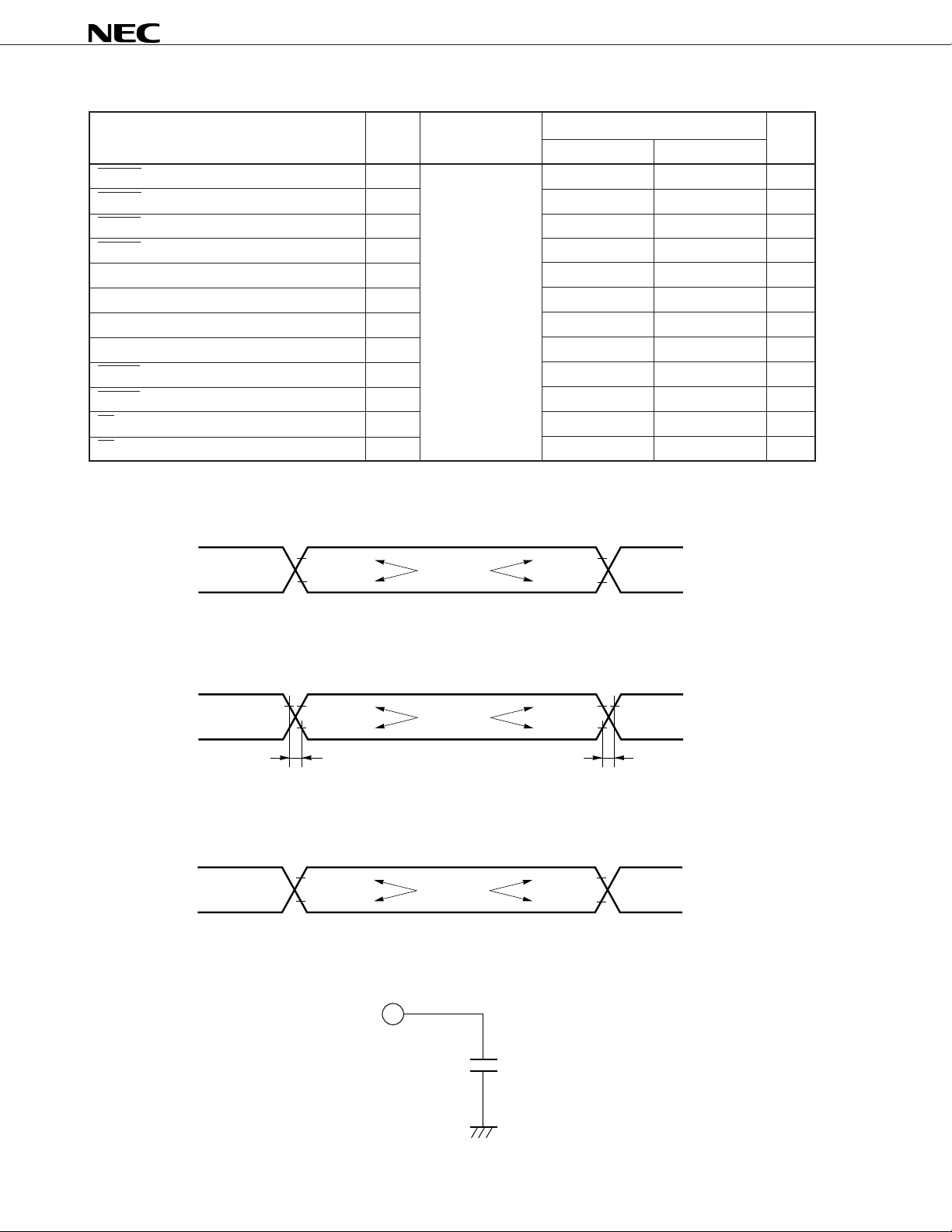
µPD70732
Bus Hold
Parameter Symbol Test Conditions µPD70732-25 Unit
MIN. MAX.
HLDRQ setup time (to CLK↓)tSHQK 8ns
HLDRQ hold time (from CLK↓)tHKHQ 5ns
HLDAK output delay time (from CLK↑)tDKHA 125ns
HLDAK output hold time (from CLK↑)tHKHA 125ns
Address, etc. delay time
Address, etc. delay time (from float, from CLK↑)
Data delay time (from active, from CLK↓)tHZKD 340ns
Data delay time (from float, from CLK↓)tLZKD 340ns
BCYST delay time (from active, from CLK↑)tHZKBC 330ns
BCYST delay time (from float, from CLK↑)tLZKBC 330ns
DA delay time (from active, from CLK↑)tHZKDA 330ns
DA delay time (from float, from CLK↑)tLZKDA 330ns
(from active, from CLK↑)
tHZKA 330ns
tLZKA 330ns
AC Test Input Waveform (Except CLK)
0.6 V
AC Test Input Waveform (CLK)
0.8 V
0.2 V
DD
DD
t
KF
0.7 V
0.3 V
DD
DD
AC Test Output Test Points
0.85 V
DD
0.4 V
Test points
Test points
Test points
2.0 V2.0 V
0.6 V
0.7 V
0.3 V
t
0.85 V
0.4 V
DD
DD
KR
DD
Load Conditions
50
V810
output pin
C
L
= 100 pF

µPD70732
10.3 Specifications When VDD = 2.2 to 3.6 V
Absolute Maximum Ratings (TA = 25˚C)
Parameter Symbol Test Conditions Rating Unit
Supply voltage VDD –0.5 to +7.0 V
Input voltage VI VDD = 2.2 to 3.6 V –0.5 to VDD + 0.3 V
Clock Input voltage VK VDD = 2.2 to 3.6 V –0.5 to VDD + 0.3 V
Output voltage VO VDD = 2.2 to 3.6 V –0.5 to VDD + 0.3 V
Operaitng ambient temperature
Storage temperature Tstg –65 to +150 ˚C
Cautions 1. Do not directly interconnect IC product output (or input/output) pins, or directly connect
V
DD or VCC to GND. However, open-drain pins and open-collector pins can be interconnected.
Direct connection is also possible for an external circuit using timing design that avoids
output collision with a pin that becomes high-impedance.
2. Product quality may suffer if the absolute maximum rating is exceeded for even a single
parameter, or even momentarily.
In other words, the absolute maximum ratings are rated values at which the product is
on the verge of suffering physical damage, and therefore, the product must be used under
conditions which ensure that the absolute maximum ratings are not exceeded. As far as
possible, the product should be used in a state in which the rated value is not approached.
The ratings and test conditions shown in the DC characteristics and AC characteristics
are the normal operation and quality assurance ranges of the product.
TA –40 to +85 ˚C
DC Characteristics (T
Parameter Symbol Test Conditions MIN. TYP. MAX. Unit
Clock input voltage, high VKH 0.8 VDD VDD + 0.3 V
Clock input voltage, low VKL –0.5 +0.2 VDD V
Input voltage, high VIH VDD ≥ 2.5 V 2.0 VDD + 0.3 V
Input voltage, low VIL –0.5 +0.2 VDD V
Output voltage, high VOH IOH = –2.0 mA 0.85 VDD V
Output voltage, low VOL IOL = 3.2 mA 0.4 V
Input leak current, high ILIH VIN = VDD 5 µA
Input leak current, low ILIL V IN = 0 V –5 µA
Output leak current, high ILOH V O = VDD 5 µA
Output leak current, low ILOL VO = 0 V –5 µA
Supply current IDD f = 10 MHz 24
A = –40 to +85˚C, VDD = 2.2 to 3.6 V)
VDD ≤ 2.5 V 0.8 VDD VDD + 0.3 V
IOH = –100 µAVDD – 0.2 V
Stopping clock
Note 1
Note 2
330µA
70 mA
Notes 1. VIL = 0 V, VIH = VDD applied
2. In general benchmark test (Output pins are open.)
Remark Operating supply current is approximately proportional to operating clock frequency.
51
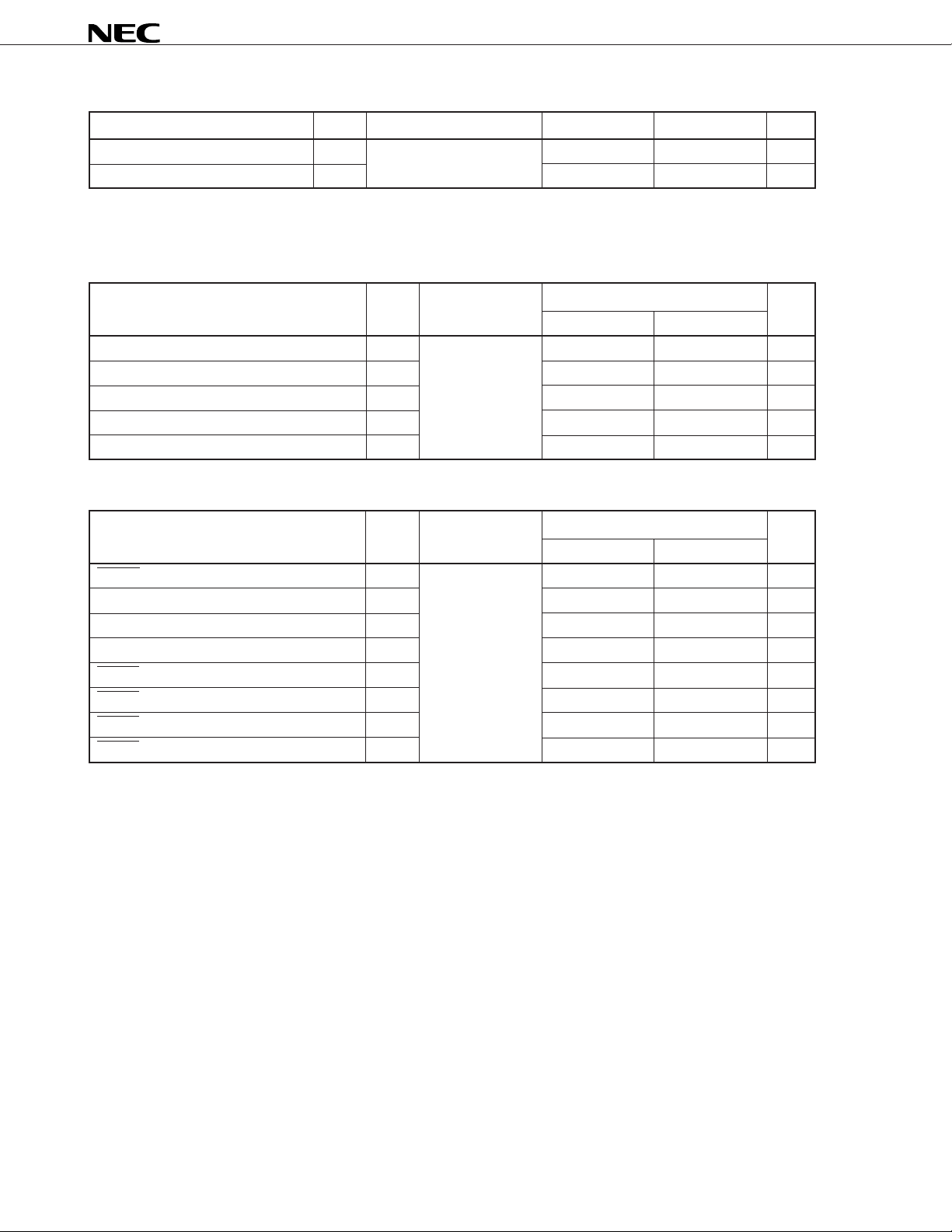
µPD70732
Capacitance (TA = 25˚C, VDD = 2.2 to 3.6 V)
Parameter Symbol Test Conditions MIN. MAX. Unit
Input capacitance CI f C = 1 MHz 15 pF
I/O capacitance CIO 15 pF
AC Characteristics (TA = –40 to +85˚C, VDD = 2.2 to 3.6 V)
Clock Input
Parameter Symbol Test Conditions µPD70732-25 Unit
MIN. MAX.
Clock cycle tCYK 100 ns
Clock pulse high-level width tKKH 40 ns
Clock pulse low-level width tKKL 40 ns
Clock rise time tKR 10 ns
Clock fall time tKF 10 ns
Reset
Parameter Symbol Test Conditions µPD70732-25 Unit
MIN. MAX.
RESET hold time (from VDD VALID) tHVR 1000 + 20tCYKR ns
Clock cycle (at reset) tCYKR 100 1000 ns
Clock high-level time (at reset) tKKHR 40 ns
Clock low-level time (at reset) tKKLR 40 ns
RESET setup time (to CLK↓, active) tSRKF 10 ns
RESET
setup time (to CLK↓, inactive)
RESET hold time (from CLK↓)tHKR 15 ns
RESET
pulse low-level width (to CLK↓)
tSRKR 10 ns
tWRL 20t CYKR ns
52

µPD70732
Memory, I/O Access
Parameter Symbol Test Conditions µPD70732-25 Unit
MIN. MAX.
Address, etc. output delay time (from CLK↑)tDKA 135ns
Address, etc. output hold time (from CLK↑)tHKA 135ns
BCYST output delay time (from CLK↑)tDKBC 135ns
BCYST output hold time (from CLK↑)tHKBC 135ns
DA output delay time (from CLK↑)tDKDA 135ns
DA output hold time (from CLK↑)tHKDA 135ns
READY setup time (to CLK↓)tSRYK 15 ns
READY hold time (from CLK↓)tHKRY 5ns
Data setup time (to CLK↑)tSDK 15 ns
Data hold time (from CLK↑)tHKD 5ns
Data output delay time (from active, from CLK↓)
Data output hold time (to active, from CLK↓)tHKDT 150ns
Data output delay time (from float, from CLK↓)
Data output hold time (to float, from CLK↓)tHZKDT 350ns
tDKDT 150ns
tLZKDT 350ns
Dynamic Bus Sizing
Parameter Symbol Test Conditions µPD70732-25 Unit
MIN. MAX.
SZRQ setup time (to CLK↓)tSSZK 15 ns
SZRQ hold time (from CLK↓)tHKSZ 5ns
Interrupt
Parameter Symbol Test Conditions µPD70732-25 Unit
MIN. MAX.
NMI setup time (to CLK↓)tSNK 15 ns
NMI hold time (from CLK↓)tHKN 5ns
INT, etc. setup time (to CLK↑)tSIK 15 ns
INT, etc. hold time (from CLK↑)tHKI 5ns
53

µPD70732
Bus Hold
Parameter Symbol Test Conditions µPD70732-25 Unit
MIN. MAX.
HLDRQ setup time (to CLK↓)tSHQK 15 ns
HLDRQ hold time (from CLK↓)tHKHQ 5ns
HLDAK output delay time (from CLK↑)tDKHA 135ns
HLDAK output hold time (from CLK↑)tHKHA 135ns
Address, etc. delay time
Address, etc. delay time (from float, from CLK↑)
Data delay time (from active, from CLK↓)tHZKD 350ns
Data delay time (from float, from CLK↓)tLZKD 350ns
BCYST delay time (from active, from CLK↑)tHZKBC 335ns
BCYST delay time (from float, from CLK↑)tLZKBC 335ns
DA delay time (from active, from CLK↑)tHZKDA 335ns
DA delay time (from float, from CLK↑)tLZKDA 335ns
(from active, from CLK↑)
tHZKA 335ns
tLZKA 335ns
AC Test Input Waveform (Except CLK)
0.8 V
DD
0.2 V
DD
AC Test Input Waveform (CLK)
0.8 V
0.2 V
DD
DD
t
KF
0.7 V
0.3 V
DD
DD
AC Test Output Test Points
0.85 V
0.4 V
0.8 V
Test points
Test points
DD
Test points
0.2 V
0.7 V
0.3 V
t
0.85 V
0.4 V
DD
DD
DD
DD
KR
DD
Load Conditions
54
V810
output pin
C
L
= 100 pF
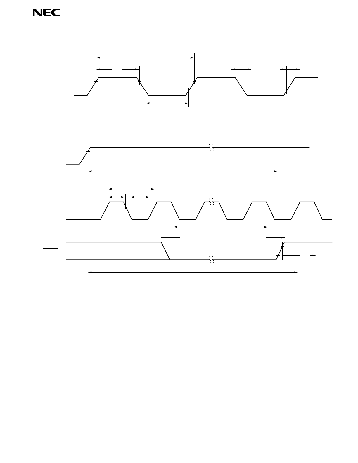
Clock Timing
CLK
Reset Timing
0.9 V
V
DD
DD
t
KKH
µPD70732
t
CYK
t
KF
t
KKL
t
HVR
t
KR
CLK
RESET
t
KKHR
t
CYKR
t
KKLR
t
SRKF
Clock stopping exception period
t
WRL
t
HKR
t
SRKR
55

Memory, I/O Access Timing
CLK
t
DKA
Note
t
DKBC
BCYST
t
HKDA
T1 T2 T2
t
HKBC
t
DKDA
µPD70732
t
HKA
t
HKDA
DA
t
SRYK
t
HKRY
t
SRYK
t
HKRY
READY
t
SDK
D31 to D0
Hi-Z
(Read)
t
LZKDT
D31 to D0
Hi-Z Hi-Z
(Write)
t
DKDT
D31 to D0
(Write)
Note A31 to A1, BE3 to BE0, R/W, MRQ, ST1, ST0, BLOCK, ADRSERR
t
HKD
Hi-Z
t
HZKDT
t
HKDT
56

Dynamic Bus Sizing Timing
CLK
SZRQ
Interrupt Timing
CLK
t
SSZK
T2
t
HKSZ
µPD70732
NMI
INT,
INTV3 to INTV0
t
SNK
t
HKN
t
SIK
t
HKI
57
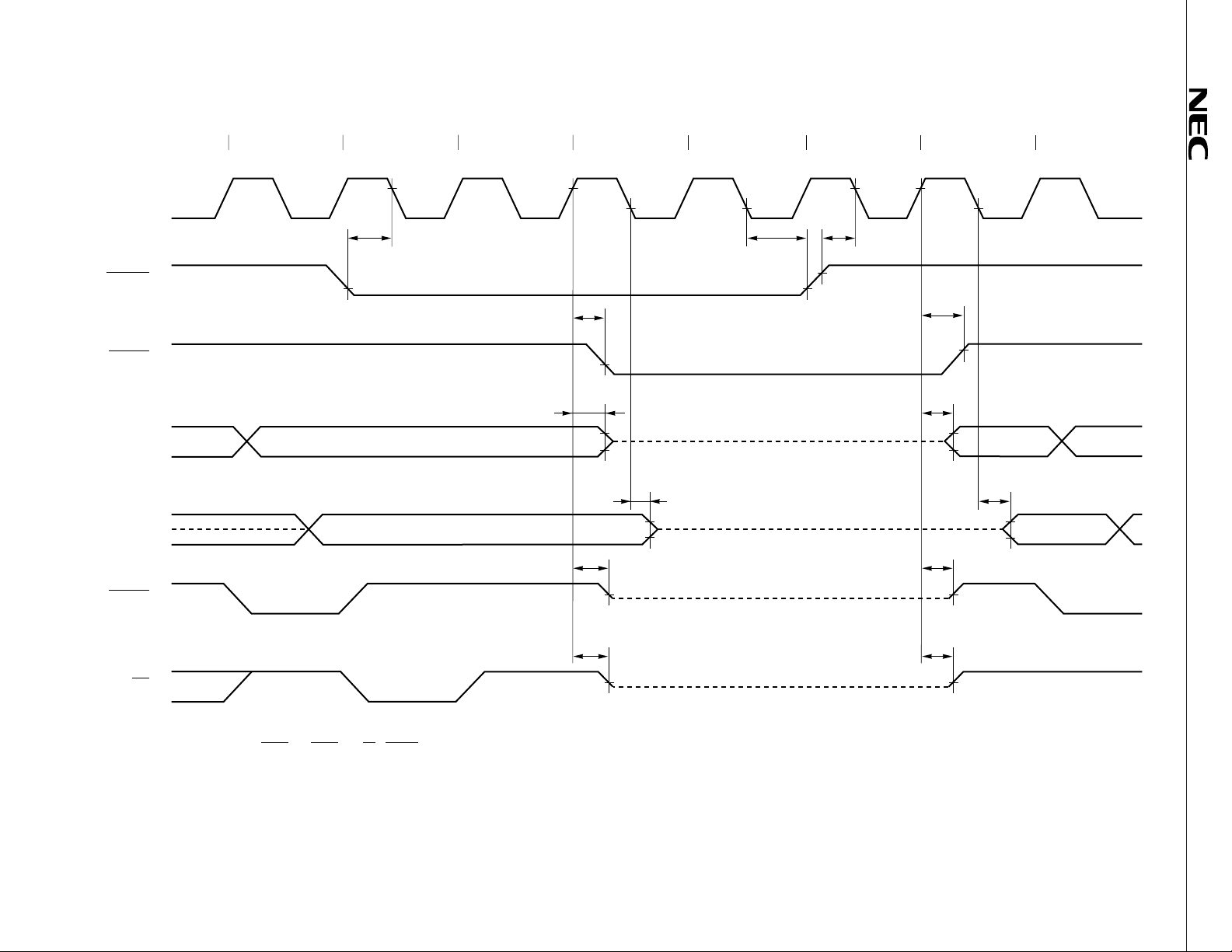
58
Bus Hold Timing
CLK
HLDRQ
HLDAK
Note 1
D31 to D0
(Write)
T1 T2 TI TH TH TH TI T1
t
SHQK
t
HZKA
t
DKHA
t
HKHQ
t
SHQK
t
t
LZKA
HKHA
Note 2
t
t
HZKD
LZKD
Note 2
t
HZKBC
t
LZKBC
BCYST
DA
Notes 1. A31 to A1, BE3 to BE0, R/W, MRQ, ST1, ST0
2. The level immediately before the high-impedance state has been stored internally.
Remark A dashed line indicates high impedance.
t
HZKDA
t
LZKDA
µPD70732
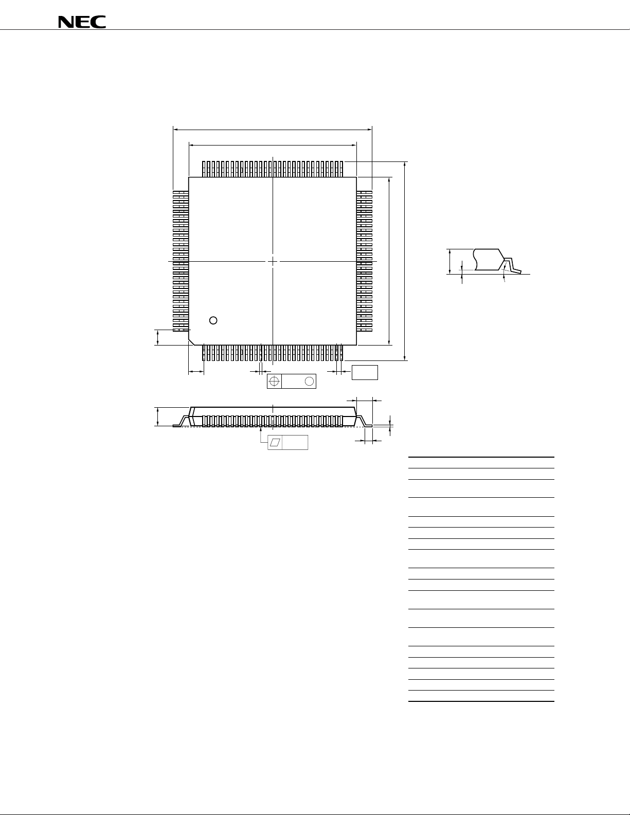
11. PACKAGE DRAWINGS
120-pin plastic QFP (28 x 28)
µPD70732
A
B
90
91
F
120 31
130
G
H
M
I
61
P
N
NOTE
Each lead centerline is located within 0.15 mm (0.006 inch) of
its true position (T.P.) at maximum material condition.
60
detail of lead end
C
D
S
Q
R
J
K
M
L
ITEM MILLIMETERS INCHES
A 32.0±0.3
28.0±0.2
B
28.0±0.2
C
D
32.0±0.3
F
2.4
G
2.4
H
0.35±0.10
I
0.15
J
0.8 (T.P.)
K
2.0±0.2
L
0.8±0.2
+0.10
0.15
M
N
P 3.2 0.126
Q
R 5°±5°
S
–0.05
0.1
0.1±0.1
3.5 MAX.
1.260±0.012
+0.009
1.102
–0.008
+0.009
1.102
–0.008
1.260±0.012
0.094
0.094
+0.004
0.014
–0.005
0.006
0.031 (T.P.)
+0.009
0.079
–0.008
+0.009
0.031
–0.008
+0.004
0.006
–0.003
0.004
0.004±0.004
5°±5°
0.138 MAX.
P120GD-80-LBB, MBB-1
59

★
120-pin plastic TQFP (Fine pitch) (14 x 14)
µPD70732
A
B
90
91
120
F
1
G
H
M
I
P
N
NOTE
Each lead centerline is located within 0.09
mm (0.004 inch) of its true position (T.P.) at
maximum material condition.
61
60
detail of lead end
D
C
S
Q
31
30
J
K
M
L
S120GC-40-9EV
ITEM MILLIMETERS INCHES
I
16.0±0.2
14.0±0.2
14.0±0.2
16.0±0.2
1.2
1.2
0.18±0.05
0.09
0.4 (T.P.)
1.0±0.2
0.5±0.2
0.145±0.05
0.08
1.0±0.1
0.1±0.05
1.2 MAX.
0.630±0.008
+0.009
0.551
–0.008
+0.009
0.551
–0.008
0.630±0.008
0.047
0.047
0.007±0.002
0.004
0.016 (T.P.)
+0.009
0.039
–0.008
+0.008
0.020
–0.009
+0.002
0.006
–0.003
0.003
+0.005
0.039
–0.004
0.004±0.002
0.048 MAX.
A
B
C
D
F
G
H
J
K
L
M
N
P
Q
S
–3°
+7°
3°
60

176-pin ceramic PGA (Seamweld)
ITEM MILLIMETERS INCHES
X176R-100A-1
A 38.1±0.4
1.500
D 38.1±0.4
1.500
E
F 2.54 (T.P.)
1.27
0.050
0.100 (T.P.)
G 2.8±0.3
0.110
H
IJ2.81
0.5 MIN.
4.57 MAX.
0.019 MIN.
0.180 MAX.
0.111
K 1.2±0.2 0.047
L 0.46±0.05
0.018
M 0.5 0.020
+0.016
–0.015
+0.016
–0.015
+0.012
–0.011
φ
φ
+0.008
–0.007
+0.002
–0.001
NOTE
Each lead centerline is located within 0.5 mm ( 0.020 inch) of
its true position (T.P.) at maximum material condition.
φ
15
14
13
12
11
10
9
8
7
6
5
4
3
2
1
Q
FE
A
D
PNMLKJHGFE CBA
J
K
L
φ
M
M
G
IH
Index mark
Orientation pin
(Bottom View)
φ
D
φ
φ
µPD70732
61
µPD70732
12. RECOMMENDED SOLDERING CONDITIONS
The µPD70732 should be soldered and mounted under the conditions recommended in the table below.
For details of recommended soldering conditions, refer to the information document “Semiconductor Device
Mounting Technology Manual” (C10535E).
For soldering methods and conditions other than those recommended below, contact an NEC sales representative.
Table 12-1. Surface Mounting Type Soldering Conditions
µPD70732GD-16-LBB : 120-pin plastic QFP (28 x 28 mm)
(1)
µPD70732GD-20-LBB : 120-pin plastic QFP (28 x 28 mm)
µPD70732GD-25-LBB : 120-pin plastic QFP (28 x 28 mm)
E specification model only
Soldering Method Soldering Conditions Recommended
Condition Symbol
Infrared reflow Package peak temperature: 235°C, Duration: 30 sec. Max. (at 210°C or above), IR35-367-2
Number of times: Twice Max., Time limit: 7 days
required at 125°C)
VPS Package peak temperature: 215°C, Duration: 40 sec. Max. (at 200°C or above), VP15-367-2
Number of times: Twice Max., Time limit: 7 days
required at 125°C)
Wave soldering Solder bath temperature: 260°C Max., Duration: 10 sec. Max., WS60-367-1
Number of times: Once, Time limit: 7 days
at 125°C), Preliminary heat temperature: 120°C Max. (Package surface temperature)
Partial heating Pin temperature: 300°C Max., Duration: 3 sec. Max. (per device side) —
Note
(thereafter 36 hours prebaking
Note
(thereafter 36 hours prebaking
Note
(thereafter 36 hours prebaking required
Note For the storage period after dry-pack decapsulation, storage conditions are Max. 25°C, 65% RH.
Caution Use of more than one soldering method should be avoided (except for partial heating).
62

µPD70732
(2) µPD70732GC-25-9EV: 120-pin plastic TQFP (Fine pitch) (14 x 14 mm)
Soldering Method Soldering Conditions Recommended
Condition Symbol
Infrared reflow Package peak temperature: 235°C, Duration: 30 sec. Max. (at 210°C or above), IR35-107-2
Number of times: Twice Max., Time limit: 7 days
required at 125°C)
VPS Package peak temperature: 215°C, Duration: 40 sec. Max. (at 200°C or above), VP15-107-2
Number of times: Twice Max., Time limit: 7 days
required at 125°C)
Partial heating Pin temperature: 300°C Max., Duration: 3 sec. Max. (per device side) —
Note
(thereafter 10 hours prebaking
Note
(thereafter 10 hours prebaking
Note For the storage period after dry-pack decapsulation, storage conditions are Max. 25°C, 65% RH.
Caution Use of more than one soldering method should be avoided (except for partial heating).
Table 12-2. Insertion Type Soldering Conditions
µPD70732R-25: 176-pin ceramic PGA (Seam weld)
Soldering Method Soldering Conditions
Wave soldering Solder bath temperature: 260°C Max., Duration: 10 sec. Max.
(Pin only)
Partial heating Pin temperature: 300°C Max., Duration: 3 sec. Max. (per one pin)
★
Caution Apply wave soldering only to the pins and be careful not to bring solder into direct contact
with the package.
63

NOTES FOR CMOS DEVICES
1 PRECAUTION AGAINST ESD FOR SEMICONDUCTORS
Note: Strong electric field, when exposed to a MOS device, can cause destruction of
the gate oxide and ultimately degrade the device operation. Steps must be taken
to stop generation of static electricity as much as possible, and quickly dissipate
it once, when it has occurred. Environmental control must be adequate. When
it is dry, humidifier should be used. It is recommended to avoid using insulators
that easily build static electricity. Semiconductor devices must be stored and
transported in an anti-static container, static shielding bag or conductive
material. All test and measurement tools including work bench and floor should
be grounded. The operator should be grounded using wrist strap. Semiconductor
devices must not be touched with bare hands. Similar precautions need to be
taken for PW boards with semiconductor devices on it.
µPD70732
2 HANDLING OF UNUSED INPUT PINS FOR CMOS
Note: No connection for CMOS device inputs can be cause of malfunction. If no
connection is provided to the input pins, it is possible that an internal input level
may be generated due to noise, etc., hence causing malfunction. CMOS devices
behave differently than Bipolar or NMOS devices. Input levels of CMOS devices
must be fixed high or low by using a pull-up or pull-down circuitry. Each unused
pin should be connected to VDD or GND with a resistor, if it is considered to have
a possibility of being an output pin. All handling related to the unused pins must
be judged device by device and related specifications governing the devices.
3 STATUS BEFORE INITIALIZATION OF MOS DEVICES
Note: Power-on does not necessarily define initial status of MOS device. Production
process of MOS does not define the initial operation status of the device.
Immediately after the power source is turned ON, the devices with reset function
have not yet been initialized. Hence, power-on does not guarantee out-pin
levels, I/O settings or contents of registers. Device is not initialized until the
reset signal is received. Reset operation must be executed immediately after
power-on for devices having reset function.
64

µPD70732
Regional Information
Some information contained in this document may vary from country to country. Before using any NEC
product in your application, please contact the NEC office in your country to obtain a list of authorized
representatives and distributors. They will verify:
• Device availability
• Ordering information
• Product release schedule
• Availability of related technical literature
• Development environment specifications (for example, specifications for third-party tools and components,
host computers, power plugs, AC supply voltages, and so forth)
• Network requirements
In addition, trademarks, registered trademarks, export restrictions, and other legal issues may also vary from
country to country.
NEC Electronics Inc. (U.S.)
Mountain View, California
Tel: 800-366-9782
Fax: 800-729-9288
NEC Electronics (Germany) GmbH
Duesseldorf, Germany
Tel: 0211-65 03 02
Fax: 0211-65 03 490
NEC Electronics (UK) Ltd.
Milton Keynes, UK
Tel: 01908-691-133
Fax: 01908-670-290
NEC Electronics Italiana s.r.1.
Milano, Italy
Tel: 02-66 75 41
Fax: 02-66 75 42 99
NEC Electronics (Germany) GmbH
Benelux Office
Eindhoven, The Netherlands
Tel:040-2445845
Fax: 040-2444580
NEC Electronics (France) S.A.
France
Tel:01-30-67 58 00
Fax: 01-30-67 58 99
NEC Electronics (France) S.A.
Spain Office
Madrid, Spain
Tel: 01-504-2787
Fax: 01-504-2860
NEC Electronics (Germany) GmbH
Scandinavia Office
Taeby Sweden
Tel: 8-63 80 820
Fax: 8-63 80 388
NEC Electronics Hong Kong Ltd.
Hong Kong
Tel:2886-9318
Fax: 2886-9022/9044
NEC Electronics Hong Kong Ltd.
Seoul Branch
Seoul, Korea
Tel: 02-528-0303
Fax: 02-528-4411
NEC Electronics Singapore Pte. Ltd.
United Square, Singapore 1130
Tel:253-8311
Fax: 250-3583
NEC Electronics Taiwan Ltd.
Taipei, Taiwan
Tel: 02-719-2377
Fax: 02-719-5951
NEC do Brasil S.A.
Sao Paulo-SP, Brasil
Tel: 011-889-1680
Fax: 011-889-1689
J96. 3
65

Reference: Electrical Characteristics for Microcomputer (IEI-601)
µPD70732
The related documents indicated in this publication may include preliminary versions. However, preliminary
versions are not marked as such.
V805, V810, and V810 Family are trademarks of NEC Corporation.
No part of this document may be copied or reproduced in any form or by any means without the prior written
consent of NEC Corporation. NEC Corporation assumes no responsibility for any errors which may appear in
this document.
NEC Corporation does not assume any liability for infringement of patents, copyrights or other intellectual property
rights of third parties by or arising from use of a device described herein or any other liability arising from use
of such device. No license, either express, implied or otherwise, is granted under any patents, copyrights or other
intellectual property rights of NEC Corporation or others.
While NEC Corporation has been making continuous effort to enhance the reliability of its semiconductor devices,
the possibility of defects cannot be eliminated entirely. To minimize risks of damage or injury to persons or
property arising from a defect in an NEC semiconductor device, customers must incorporate sufficient safety
measures in its design, such as redundancy, fire-containment, and anti-failure features.
NEC devices are classified into the following three quality grades:
"Standard", "Special", and "Specific". The Specific quality grade applies only to devices developed based on a
customer designated "quality assurance program" for a specific application. The recommended applications of
a device depend on its quality grade, as indicated below. Customers must check the quality grade of each device
before using it in a particular application.
Standard: Computers, office equipment, communications equipment, test and measurement equipment,
audio and visual equipment, home electronic appliances, machine tools, personal electronic
equipment and industrial robots
Special: Transportation equipment (automobiles, trains, ships, etc.), traffic control systems, anti-disaster
systems, anti-crime systems, safety equipment and medical equipment (not specifically designed
for life support)
Specific: Aircrafts, aerospace equipment, submersible repeaters, nuclear reactor control systems, life
support systems or medical equipment for life support, etc.
The quality grade of NEC devices is "Standard" unless otherwise specified in NEC's Data Sheets or Data Books.
If customers intend to use NEC devices for applications other than those specified for Standard quality grade,
they should contact an NEC sales representative in advance.
Anti-radioactive design is not implemented in this product.
M4 96.5
 Loading...