

Page 1
PRELIMINARY DATA SHEET
MOS INTEGRATED CIRCUIT
PD4664312-X
µµµµ
64M-BIT CMOS MOBILE SPECIFIED RAM
4M-WORD BY 16-BIT
EXTENDED TEMPERATURE OPERATION
Description
The µPD4664312-X is a high speed, low power, 67,108,864 bits (4,194,304 words by 16 bits) CMOS Mobile
Specified RAM featuring Low Power Static RAM compatible function and pin configuration.
The
PD4664312-X is fabricated with advanced CMOS technology using one-transistor memory cell.
µ
The
PD4664312-X is packed in 93-pin TAPE FBGA.
µ
Features
• 4,194,304 words by 16 bits organization
• Fast access time: 65, 75 ns (MAX.)
• Fast page access time: 18, 25 ns (MAX.)
• Byte data control: /LB (I/O0 to I/O7), /UB (I/O8 to I/O15)
• Low voltage operation:2.7 to 3.1 V (-B65X)
2.7 to 3.1 V (Chip), 1.65 to 2.1 V (I/O) (-BE75X)
= –25 to +85 °C
• Operating ambient temperature: T
• Output Enable input for easy application
• Chip Enable input: /CS pin
• Standby Mode input: MODE pin
• Standby Mode1: Normal standby (Memory cell data hold valid)
• Standby Mode2: Density of memory cell data hold is variable
A
PD4664312 Access Operating supply Operating Supply current
µ
time voltage ambient At operating At standby µA (MAX.)
ns (MAX.) V temperature mA (MAX.) Density of data hold
Chip I/O °C 64M bits 16M bits 8M bits 4M bits 0M bit
-B65X 65 2.7 to 3.1 – –25 to +85 45 100 60 50 45 10
Note
-BE75X
Note Under development
The information in this document is subject to change without notice. Before using this document, please
confirm that this is the latest version.
Not all devices/types available in every country. Please check with local NEC representative for
availability and additional information.
Document No. M15867EJ5V0DS00 (5th edition)
Date Published August 2002 NS CP (K)
Printed in Japan
75 2.7 to 3.1 1.65 to 2.1 40
The mark shows major revised points.
©
2001
Page 2

PD4664312-X
µµµµ
Ordering Information
Part number Package Access time Operating supply voltage Operating
ns (MAX.) V temperature
Chip I/O °C
PD4664312F9-B65X-CR2 93-pin TAPE FBGA (12 x 9) 65 2.7 to 3.1 – –25 to +85
µ
PD4664312F9-BE75X-CR2
µ
Note Under development
Note
75 2.7 to 3.1 1.65 to 2.1
2
Preliminary Data Sheet M15867EJ5V0DS
Page 3
Pin Configurations
/xxx indicates active low signal.
93-pin TAPE FBGA (12 x 9)
PD4664312F9-B65X-CR2 ]
[
µµµµ
PD4664312-X
µµµµ
10
Top View
P
BCDEFGHJKLM
A
ABCDEFGH
NC
NC
NC
NC
A15
A11
A8
/WE V
NC
/LB
A7 /OE
NC
NCNC
A12
A19
MODE A20
/UB
9
8
7
6
5
4
3
2
1
N
NC NCNC NC
A21 NC GND
A13
A18
A5 I/O8
A14
A10
NC
NC
A17
A4
A1A2
10
9
8
7
6
5
4
3
2
1
Top View
A16
NC
I/O6 I/O13A9
NC
NC
I/O1
GND
A0A3
NCNC
Bottom View
NP
M
LKJHGFEDCBA
NC
NC
/CS
I/O14
I/O5
NC
CC
I/O11NCNC
I/O2
I/O15
I/O4
I/O3
I/O9
NC
I/O7
I/O12
I/O10
I/O0A6
MKLJ
NC NC
NCNC
NCNC
NCNC
NCNC
NCNC
NCNC
N
NC
NC
NCNC
P
NC
NC
A0 to A21 : Address inputs
I/O0 to I/O15 : Data inputs / outputs
/CS : Chip Select
MODE : Standby mode
/LB, /UB : Byte data select
V
CC
GND : Ground
Note
NC
/WE : W rite enable
/OE : Output enable
Note Some signals can be applied because this pin is not internally connected.
Remarks Refer to Package Drawing for the index mark.
Preliminary Data Sheet M15867EJ5V0DS
: Power supply
: No Connection
3
Page 4
93-pin TAPE FBGA (12 x 9)
PD4664312F9-BE75X-CR2 ]
[
µµµµ
PD4664312-X
µµµµ
10
Top View
P
BCDEFGHJKLM
A
ABCDEFGH
NC
NC
NC
NC
A15
A11
A8
/WE V
NC
/LB
A7 /OE
NC
NCNC
A12
A19
MODE A20
/UB
9
8
7
6
5
4
3
2
1
N
NC NCNC NC
A21 NC GND
A13
A18
A5 I/O8
A14
A10
NC
NC
A17
A4
A1A2
10
9
8
7
6
5
4
3
2
1
Top View
A16
NC
I/O6 I/O13A9
NC
NC
I/O1
GND
A0A3
NCNC
Bottom View
NP
M
LKJHGFEDCBA
NC
NC
/CS
I/O14
I/O5
CC
CC
Q
V
I/O11NCNC
I/O2
I/O15
I/O4
I/O3
I/O9
NC
I/O7
I/O12
I/O10
I/O0A6
MKLJ
NC NC
NCNC
NCNC
NCNC
NCNC
NCNC
NCNC
N
NC
NC
NCNC
P
NC
NC
A0 to A21 : Address inputs
I/O0 to I/O15 : Data inputs / outputs
/CS : Chip Select
MODE : Standby mode
/WE : W rite enable
/LB, /UB : Byte data select
V
CC
V
Q : Input / Output power supply
CC
GND : Ground
Note
NC
/OE : Output enable
Note Some signals can be applied because this pin is not internally connected.
Remarks Refer to Package Drawing for the index mark.
4
Preliminary Data Sheet M15867EJ5V0DS
: Power supply
: No Connection
Page 5
Block Diagram
V
CC
VCCQ
Refresh
control
Standby mode control
PD4664312-X
µµµµ
GND
A0
A21
I/O0 to I/O7
I/O8 to I/O15
/CS
Refresh
counter
Address
buffer
Row
decoder
Input data
controller
Memory cell array
67,108,864 bits
Sense amplifier /
Switching circuit
Column decoder
Address buffer
Output data
controller
MODE
/LB
/UB
/WE
/OE
Remark VCCQ is the input / output power supply for -BE75X.
Preliminary Data Sheet M15867EJ5V0DS
5
Page 6
PD4664312-X
µµµµ
Truth Table
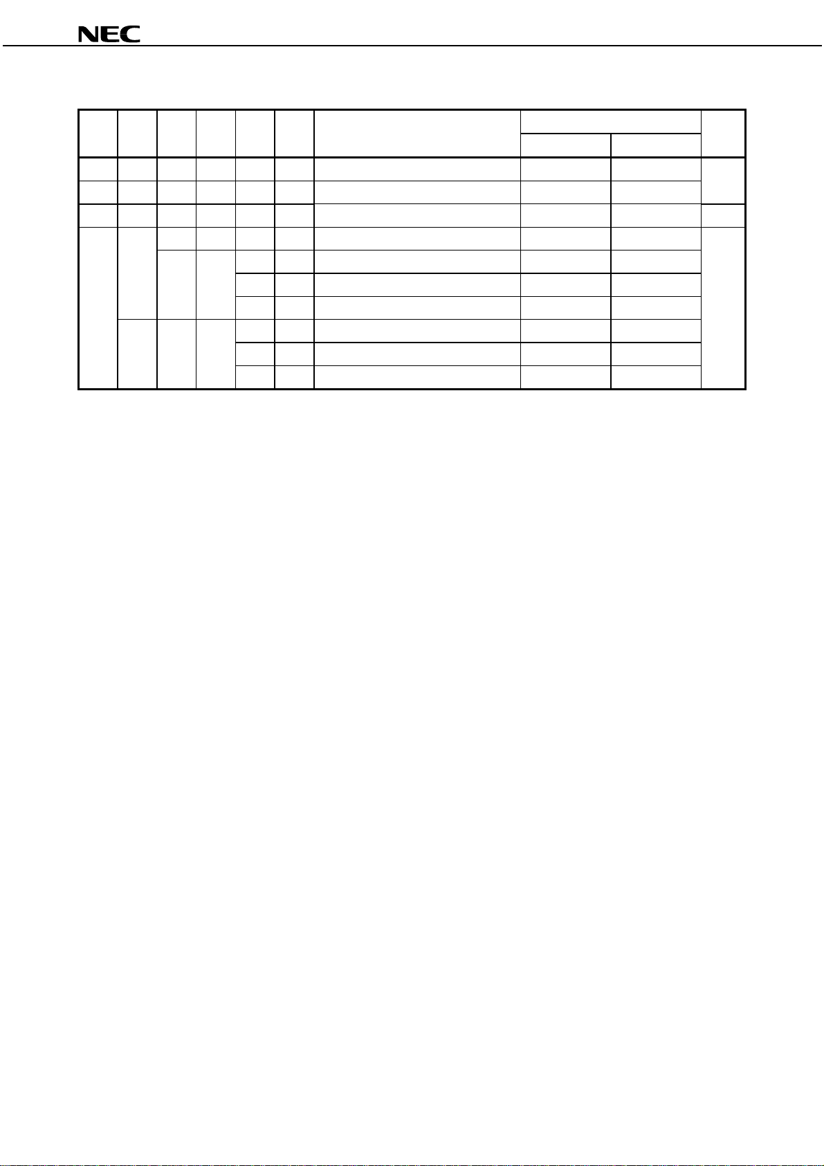
/CS MODE /OE /WE /LB /UB Mode I/O Supply
I/O0 to I/O7 I/O8 to I/O15 current
HH×××× Not selected (Standby Mode 1) High-Z High-Z I
× H ××H H Not selected (Standby Mode 1) High-Z High-Z
× L ×××× Not selected (Standby Mode 2)
Note
High-Z High-Z I
LHHH×× Output disable High-Z High-Z I
L H L L Word read D
L H Lower byte read D
OUT
OUT
H L Upper byte read High-Z D
HLLL Word write D
L H Lower byte write D
IN
IN
H L Upper byte write High-Z D
OUT
D
High-Z
OUT
IN
D
High-Z
IN
Note MODE pin must be fixed to high level except Standby Mode 2. (refer to 2.3 Standby Mode Status Transition).
Remark ×: VIH
or VIL, H: VIH, L: V
IL
SB1
SB2
CCA
6
Preliminary Data Sheet M15867EJ5V0DS
Page 7

PD4664312-X
µµµµ
CONTENTS
1. Initialization .................................................................................................................................................................... 8
2. Partial Refresh ............................................................................................................................................................... 9
2.1 Standby Mode........................................................................................................................................................... 9
2.2 Density Switching......................................................................................................................................................9
2.3 Standby Mode Status Transition............................................................................................................................... 9
2.4 Addresses for Which Partial Refresh Is Supported ................................................................................................ 10
3. Page Read Operation .................................................................................................................................................. 11
3.1 Features of Page Read Operation.......................................................................................................................... 11
3.2 Page Length ...........................................................................................................................................................11
3.3 Page-Corresponding Addresses............................................................................................................................. 11
3.4 Page Start Address................................................................................................................................................. 11
3.5 Page Direction ........................................................................................................................................................ 11
3.6 Interrupt during Page Read Operation.................................................................................................................... 11
3.7 When page read is not used................................................................................................................................... 11
4. Mode Register Settings................................................................................................................................................ 12
4.1 Mode Register Setting Method ............................................................................................................................... 12
4.2 Cautions for Setting Mode Register........................................................................................................................ 13
5. Electrical Specifications ............................................................................................................................................... 14
6. Timing Charts............................................................................................................................................................... 20
7. Package Drawing......................................................................................................................................................... 30
8. Recommended Soldering Conditions ..........................................................................................................................31
9. Revision History ........................................................................................................................................................... 32
Preliminary Data Sheet M15867EJ5V0DS
7
Page 8
PD4664312-X
µµµµ
1. Initialization
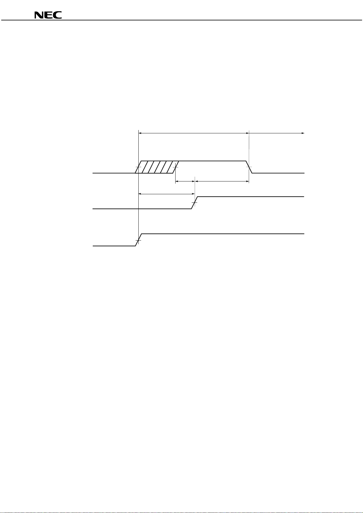
Initialize the µPD4664312-X at power application using the following sequence to stabilize internal circuits.
(1) Following power application, make MODE high level after fixing MODE to low level for the period of t
/CS high level before making MODE high level.
(2) /CS and MODE are fixed to high level for the period of t
Normal operation is possible after the completion of initialization.
Figure1-1. Initialization Timing Chart
MHCL
.
VHMH
. Make
Initialization
/CS (Input)
t
CHMH
t
VHMH
MODE (Input)
V
CC
VCC (MIN.)
Cautions 1. Make MODE low level when starting the power supply.
2. t
is specified from when the power supply voltage reaches the prescribed minimum value (V
VHMH
(MIN.)).
t
MHCL
Normal Operation
CC
8
Preliminary Data Sheet M15867EJ5V0DS
Page 9

PD4664312-X
µµµµ
2. Partial Refresh
2.1 Standby Mode
In addition to the regular standby mode (Standby Mode 1) with a 64M bits density, Standby Mode 2, which performs
partial refresh, is also provided.
2.2 Density Switching
In Standby Mode 2, the densities that can be selected for performing refresh are 16M bits, 8M bits, 4M bits, and 0M bit.
The density for performing refresh can be set with the mode register. Once the refresh density has been set in the
mode register, these settings are retained until they are set again, while applying the power supply. However, the mode
register setting will become undefined if the power is turned off, so set the mode register again after power application.
(For how to perform mode register settings, refer to section 4. Mode Register Settings.)
2.3 Standby Mode Status Transition
In Standby Mode 1, MODE and /CS are high level, or MODE, /LB and /UB are high level. In Standby Mode 2, MODE is
low level. In Standby Mode 2, if 0M bit is set as the density, it is necessary to perform initialization the same way as after
applying power, in order to return to normal operation from Standby Mode 2. When the density has been set to 16M bits,
8M bits, or 4M bits in Standby Mode 2, it is not necessary to perform initialization to return to normal operation from
Standby Mode 2.
For the timing charts, refer to Figure 6-14. Standby Mode 2 (data hold: 16M bits / 8M bits / 4M bits) Entry / Exit
Timing Chart, Figure 6-15. Standby Mode 2 (data not held) Entry / Exit Timing Chart.
Preliminary Data Sheet M15867EJ5V0DS
9
Page 10
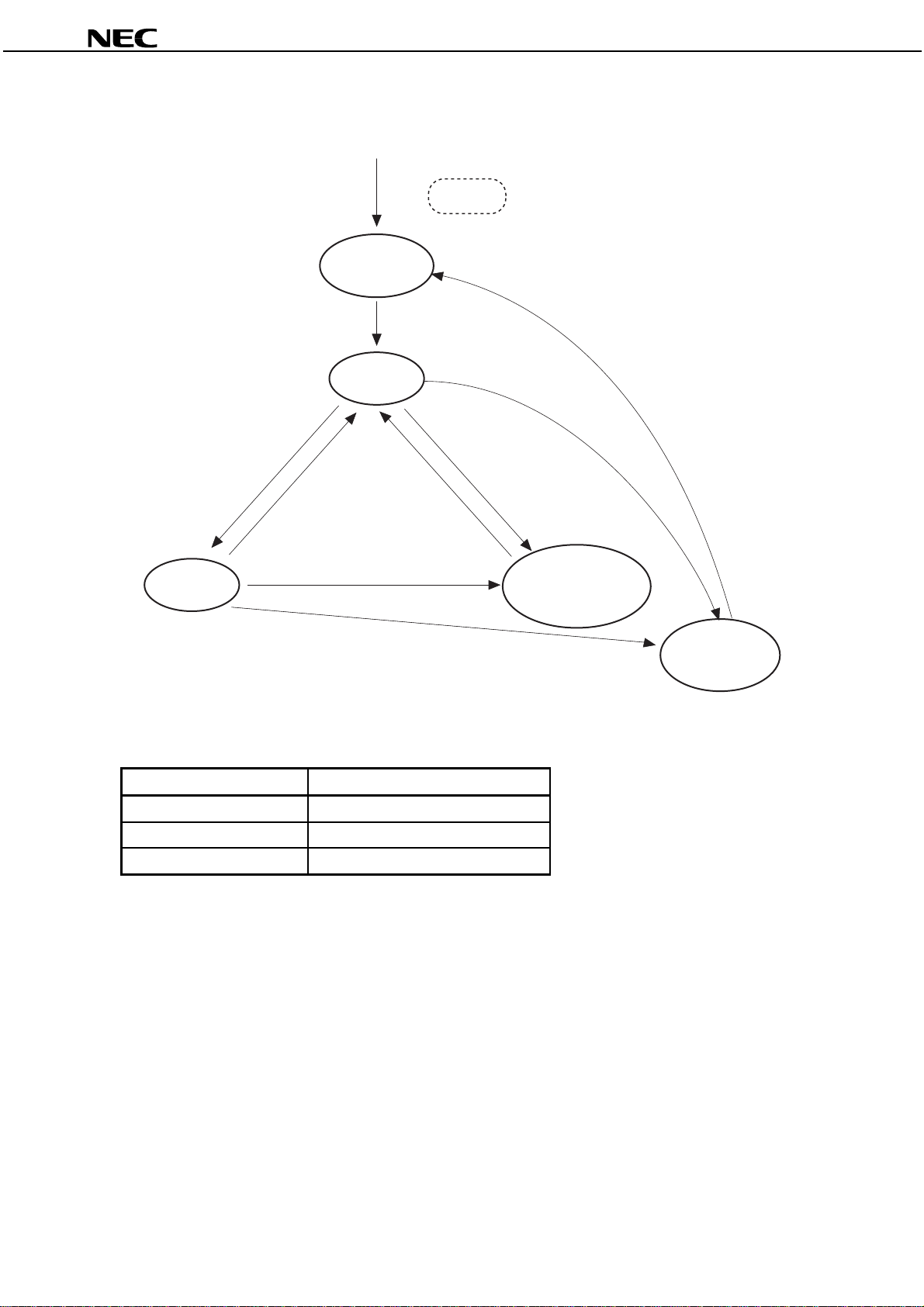
Figure 2-1. Standby Mode State Machine
Power On
Initialization
Initial State
PD4664312-X
µµµµ
IL
MODE = VIH,
/CS = VIH or
/LB, /UB = VIH
Standby
Mode 1
/CS = VIL,
MODE = VIH
/CS = V
Active
/CS = VIL,
MODE = V
MODE = VIL
MODE = VIL
2.4 Addresses for Which Partial Refresh Is Supported
MODE = VIH
MODE = VIL
MODE = VIL
IH
Standby Mode 2
(16M bits / 8M bits
/ 4M bits)
Standby Mode 2
(Data not held)
Data hold density Correspondence address
16M bits 000000H to 0FFFFFH
8M bits 000000H to 07FFFFH
4M bits 000000H to 03FFFFH
10
Preliminary Data Sheet M15867EJ5V0DS
Page 11

3. Page Read Operation
3.1 Features of Page Read Operation
Features 8 Words Mode
Page length 8 words
Page read-corresponding addresses A2, A1, A0
Page read start address Don’t care
Page direction Don’t care
Interrupt during page read operation Enabled
Note An interrupt is output when /CS = H or in case A3 or a higher address changes.
3.2 Page Length
8 words is supported as the page lengths.
Note
PD4664312-X
µµµµ
3.3 Page-Corresponding Addresses
The page read-enabled addresses are A2, A1, and A0. Fix addresses other than A2, A1, and A0 during page read
operation.
3.4 Page Start Address
Since random page read is supported, any address (A2, A1, A0) can be used as the page read start address.
3.5 Page Direction
Since random page read is possible, there is not restriction on the page direction.
3.6 Interrupt during Page Read Operation
When generating an interrupt during page read, either make /CS high level or change A3 and higher addresses.
3.7 When page read is not used
Since random page read is supported, even when not using page read, random access is possible as usual.
Preliminary Data Sheet M15867EJ5V0DS
11
Page 12
PD4664312-X
µµµµ
4. Mode Register Settings
The partial refresh density can be set using the mode register. Since the initial value of the mode register at power
application is undefined, be sure to set the mode register after initialization at power application. When setting the
density of partial refresh, data before entering the partial refresh mode is not guaranteed. (This is the same for re-
setup.) However, since partial refresh mode is not entered unless MODE = L when partial refresh is not used, it is not
necessary to set the mode register. Moreover, when using page read without using partial refresh, it is not necessary to
set the mode register.
4.1 Mode Register Setting Method
The mode register setting mode can be entered by successively writing two specific data after two continuous reads of
the highest address (3FFFFFH). The mode register setting is a continuous four-cycle operation (two read cycles and two
write cycles).
Commands are written to the command register. The command register is used to latch the addresses and data
required for executing commands, and it does not have an exclusive memory area.
For the timing chart and flow chart, refer to Figure 6-12. Mode Register Setting Timing Chart, Figure 6-13. Mode
Register Setting Flow Chart.
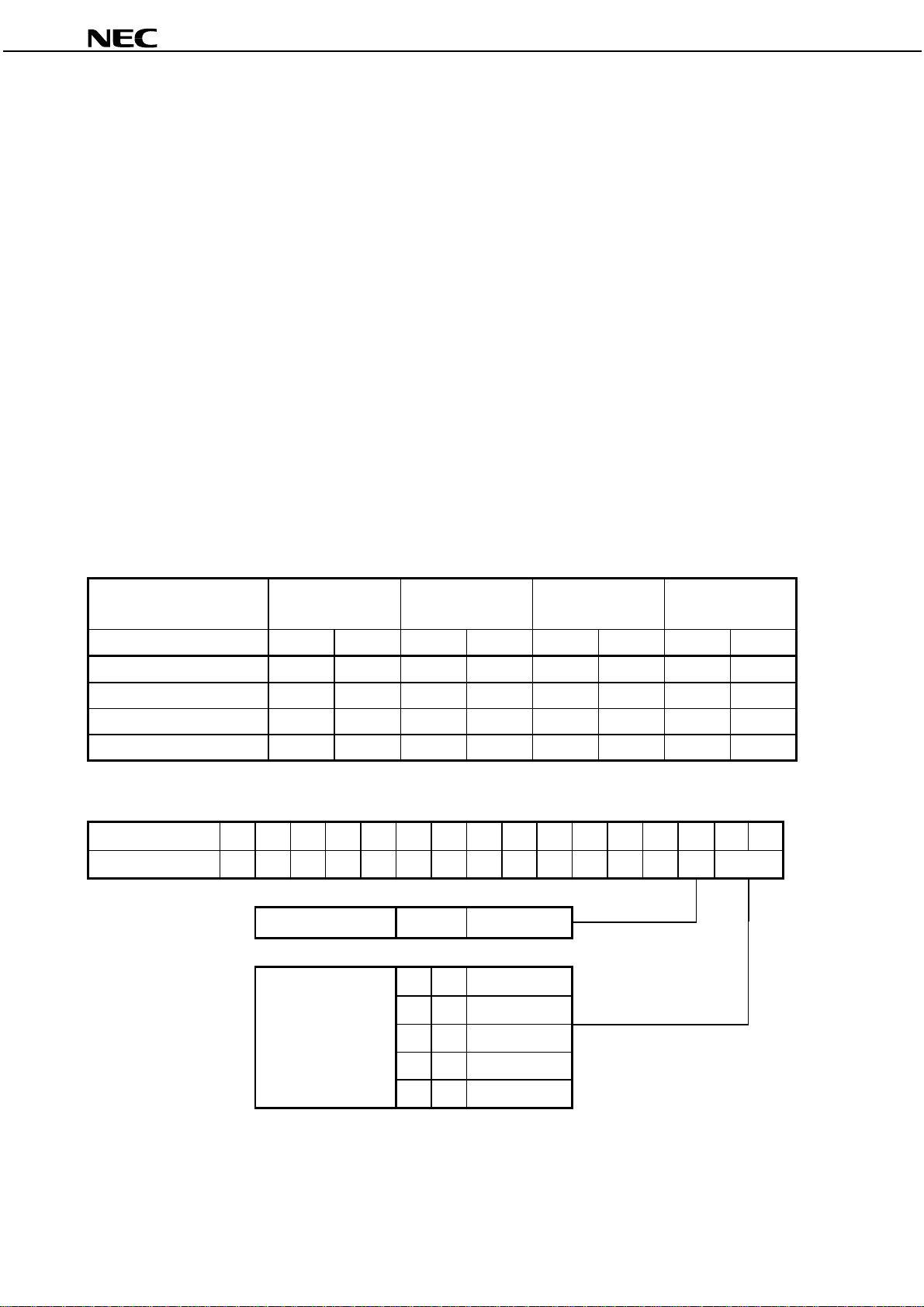
Table 4-1. shows the commands and command sequences.
Table 4-1. Command sequence
Command sequence 1st bus cycle 2nd bus cycle 3rd bus cycle 4th bus cycle
(Read cycle) (Read cycle) (Write cycle) (Write cycle)
Partial refresh density Address Data Address Data Address Data Address Data
16M bits 3FFFFFH – 3FFFFFH – 3FFFFFH 00H 3FFFFFH 04H
8M bits 3FFFFFH – 3FFFFFH – 3FFFFFH 00H 3FFFFFH 05H
4M bits 3FFFFFH – 3FFFFFH – 3FFFFFH 00H 3FFFFFH 06H
0M bit 3FFFFFH – 3FFFFFH – 3FFFFFH 00H 3FFFFFH 07H
4th bus cycle (Write cycle)
I/O 1514131211109876543210
Mode Register setting 0000000000000PL PD
Page length 1 8 words
I/O1 I/O0 Density
12
Partial refresh 0 0 16M bits
density 0 1 8M bits
1 0 4M bits
1 1 0M bit
Preliminary Data Sheet M15867EJ5V0DS
Page 13

PD4664312-X
µµµµ
4.2 Cautions for Setting Mode Register
Since, for the mode register setting, the internal counter status is judged by toggling /CS and /OE, toggle /CS at every
cycle during entry (read cycle twice, write cycle twice), and toggle /OE like /CS at the first and second read cycles.
If incorrect addresses or data are written, or if addresses or data are written in the incorrect order, the setting of the
mode register is not performed correctly.
When the highest address (3FFFFFH) is read consecutively three or more times, the mode register setting entries are
not performed correctly. (Immediately after the highest address is read, the setting of the mode register is not performed
correctly.) Perform the setting of the mode register after power application or after accessing other than the highest
address.
Once the refresh density has been set in the mode register, these settings are retained until they are set again, while
applying the power supply. However, the mode register setting will become undefined if the power is turned off, so set
the mode register again after power application.
For the timing chart and flow chart, refer to Figure 6-12. Mode Register Setting Timing Chart, Figure 6-13. Mode
Register Setting Flow Chart.
Preliminary Data Sheet M15867EJ5V0DS
13
Page 14

PD4664312-X
µµµµ
5. Electrical Specifications
Absolute Maximum Ratings
Parameter Symbol Condition Rating Unit
-B65X -BE75X
Supply voltage V
CC
Note
–0.5
to +4.0 –0.5
Input / Output supply voltage VCCQ – –0.5
Input / Output voltage V
Operating ambient temperature T
Storage temperature T
T
A
stg
Note
–0.5
to VCC + 0.4 (4.0 V MAX.)–0.5
–25 to +85 –25 to +85 °C
–55 to +125 –55 to +125 °C
Note
Note –1.0 V (MIN.) (Pulse width: 30 ns)
Caution Exposing the device to stress above those listed in Absolute Maximum Rating could cause permanent
damage. The device is not meant to be operated under conditions outside the limits described in the
operational section of this specification. Exposure to Absolute Maximum Rating conditions for
extended periods may affect device reliability.
Note
to +4.0 V
Note
to +4.0 V
to VCCQ + 0.4 (4.0 V MAX.)V
Recommended Operating Conditions
Parameter Symbol Condition -B65X -BE75X Unit
MIN. MAX. MIN. MAX.
Supply voltage V
CC
2.7 3.1 2.7 3.1 V
Input / Output supply voltage VCCQ – – 1.65 2.1 V
High level input voltage V
Low level input voltage V
Operating ambient temperature T
IH
IL
A
0.8V
–0.3
CC
Note
VCC+0.3 0.8VCCQV
0.2V
CC
–0.3
Note
CC
Q+0.3 V
0.2VCCQV
–25 +85 –25 +85 °C
Note –0.5 V (MIN.) (Pulse width: 30 ns)
Capacitance (TA = 25°°°°C, f = 1 MHz)
Parameter Symbol Test condition MIN. TYP. MAX. Unit
Input capacitance C
Input / Output capacitance C
Remarks 1. VIN: Input voltage, V
IN
VIN = 0 V 8 pF
I/O
I/O
V
= 0 V 10 pF
: Input / Output voltage
I/O
2. These parameters are not 100% tested.
14
Preliminary Data Sheet M15867EJ5V0DS
Page 15

DC Characteristics (Recommended Operating Conditions Unless Otherwise Noted) (1/2)
Parameter Symbol Test condition Density of -B65X Unit
data hold MIN. TYP. MAX.
PD4664312-X
µµµµ
Input leakage current ILIV
I/O leakage current I
Operating supply current I
Standby supply current I
LOVI/O
CCA
SB1
SB2
I
IN
= 0 V to V
= 0 V to VCC, /CS = V
/WE = VIL or /OE = V
/CS = VIL, Minimum cycle time, 45 mA
I/O
I
= 0 mA
/CS ≥ V
MODE ≥ V
/CS ≥ V
CC
IH
or –1.0 +1.0
IH
CC
− 0.2 V, 64M bits 60 100
CC
− 0.2 V
CC
− 0.2 V, 16M bits 50 60
–1.0 +1.0
MODE ≤ 0.2 V 8M bits 45 50
4M bits 40 45
0M bit 10
High level output voltage VOHI
Low level output voltage VOLI
Remark VIN: Input voltage, V
: Input / Output voltage
I/O
OH
= –0.5 mA 0.8V
OL
= 1 mA 0.2V
CC
DC Characteristics (Recommended Operating Conditions Unless Otherwise Noted) (2/2)
Parameter Symbol Test condition Density of -BE75X Unit
data hold MIN. TYP. MAX.
A
µ
A
µ
A
µ
V
CC
V
Input leakage current I
I/O leakage current I
Operating supply current I
Standby supply current
High level output voltage V
Low level output voltage V
Remark VIN: Input voltage, V
LI
IN
V
= 0 V to VCCQ –1.0 +1.0
LO
I/O
V
= 0 V to VCCQ, /CS = V
IL
/WE = V
CCA
/CS = VIL, Minimum cycle time, 40 mA
I/O
I
ISB1
/CS ≥ V
MODE ≥ V
SB2
I
/CS ≥ V
or /OE = V
= 0 mA
CC
− 0.2 V, 64M bits 60 100
CC
CC
− 0.2 V, 16M bits 50 60
MODE ≤ 0.2 V 8M bits 45 50
OHIOH
OLIOL
: Input / Output voltage
I/O
= –0.5 mA 0.8VCCQV
= 1 mA 0.2VCCQV
− 0.2 V
IH
or –1.0 +1.0
IH
4M bits 40 45
0M bit 10
A
µ
A
µ
A
µ
Preliminary Data Sheet M15867EJ5V0DS
15
Page 16

AC Characteristics (Recommended Operating Conditions Unless Otherwise Noted)
AC Test Conditions
[ -B65X ]
Input Waveform (Rise and Fall Time ≤≤≤≤ 5 ns)
Vcc
0.8Vcc
Vcc / 2
Test points
Vcc / 2
0.2Vcc
GND
5ns
Output Waveform
Test pointsVcc / 2 Vcc / 2
PD4664312-X
µµµµ
[ -BE75X ]
Input Waveform (Rise and Fall Time ≤≤≤≤ 5 ns)
VccQ
0.8VccQ
VccQ / 2
Test points
VccQ / 2
0.2VccQ
GND
5ns
Output Waveform
Test pointsVccQ / 2 VccQ / 2
Output Load
AC characteristics directed with the note should be measured with the output load shown in Figure 5-1, Figure 5-2.
Figure 5-1. Figure 5-2.
[ -B65X ] [ -BE75X ]
C
: 30 pF CL: 30 pF
L
5 pF (t
CLZ
, t
, t
, t
, t
, t
OLZ
BLZ
CHZ
OHZ
) 5 pF (t
BHZ
CLZ
, t
, t
, t
, t
, t
OLZ
BLZ
CHZ
OHZ
BHZ
)
16
I/O (Output)
Z
O = 50 Ω
I/O (Output)
C
50 Ω
VCC / 2
Preliminary Data Sheet M15867EJ5V0DS
L
O = 50 Ω
Z
VCCQ / 2
50 Ω
C
L
Page 17
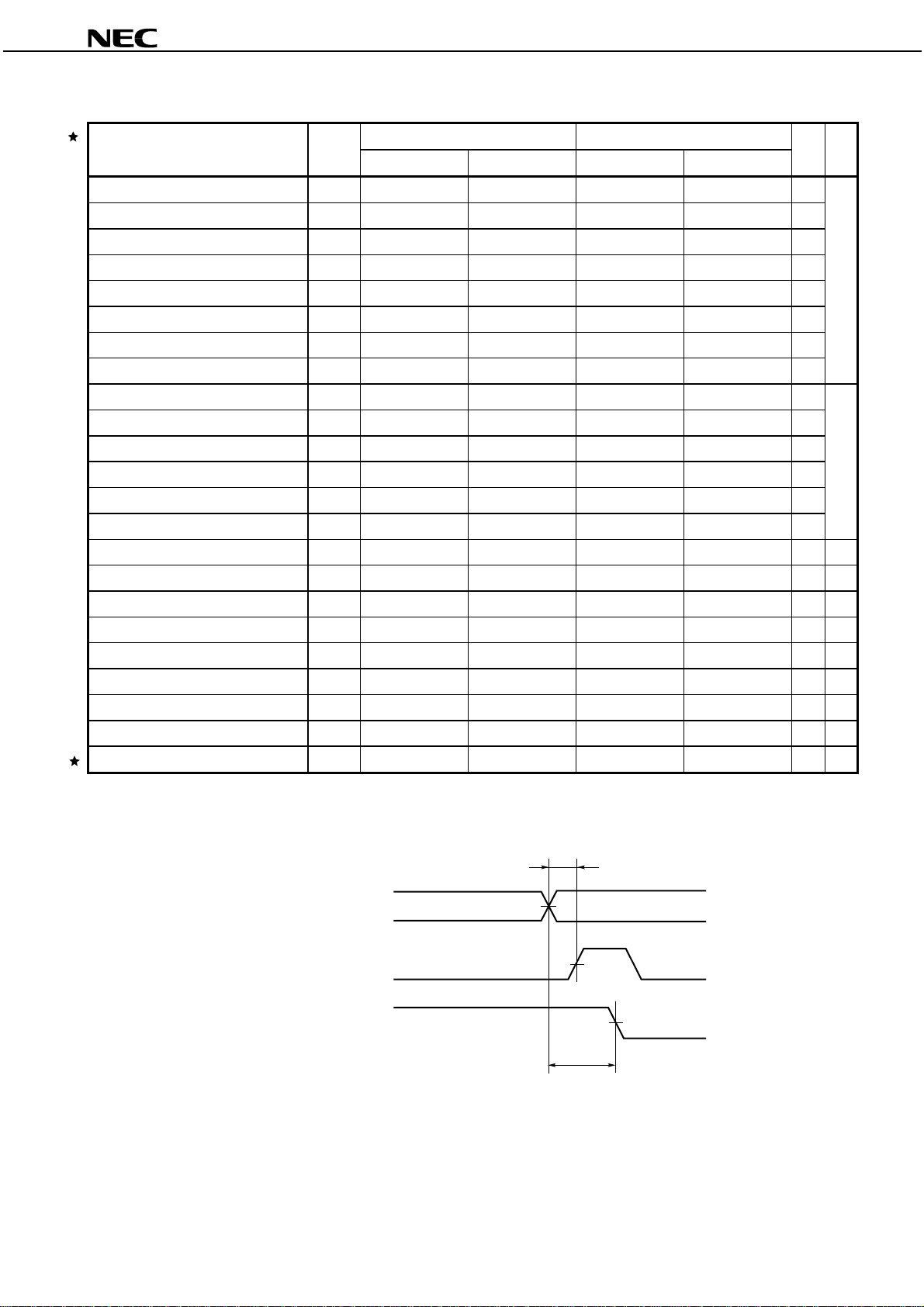
Read Cycle
PD4664312-X
µµµµ
Parameter Symbol -B65X -BE75X Unit Note
MIN. MAX. MIN. MAX.
Read cycle time t
Address access time t
/CS access time t
/OE to output valid t
/LB, /UB to output valid t
Output hold from address change t
Page read cycle time t
Page access time t
/CS to output in low impedance t
/OE to output in low impedance t
/LB, /UB to output in low impedance t
/CS to output in high impedance t
/OE to output in high impedance t
/LB, /UB to output in high impedance t
Address set to /OE low level t
/OE high level to address hold t
/CS high level to address hold t
/LB, /UB high level to address hold t
/CS low level to /OE low level t
/OE low level to /CS high level t
/CS high level pulse width t
/LB, /UB high level pulse width t
/OE high level pulse width t
RC
AA
ACS
OE
BA
OH
PRC
PAA
CLZ
OLZ
BLZ
CHZ
OHZ
BHZ
ASO
OHAH
CHAH
BHAH
CLOL
OLCH
CP
BP
OP
65 75 ns 1
65 75 ns
65 75 ns
45 50 ns
65 75 ns
55ns
18 25 ns
18 25 ns
10 10 ns 2
55ns
55ns
25 25 ns
25 25 ns
25 25 ns
00ns
–5 –5 ns
00ns3
0 0 ns 3, 4
0 10,000 0 10,000 ns 5
45 45 ns
10 10 ns
10 10 ns
2 10,000 2 10,000 ns 5
Notes 1. Output load: 30 pF
2. Output load: 5 pF
3. When t
4. t
BHAH
5. t
CLOL
≥ | t
ASO
CHAH
is specified from when both /LB and /UB become high level.
and tOP (MAX.) are applied while /CS is being hold at low level.
|, | t
BHAH
|, t
CHAH
Address (Input)
/LB, /UB, /CS (Input)
/OE (Input)
Preliminary Data Sheet M15867EJ5V0DS
and t
(MIN.) are –15 ns.
BHAH
t
ASO
t
CHAH
, t
BHAH
17
Page 18

Write Cycle
PD4664312-X
µµµµ
Parameter Symbol -B65X -BE75X Unit Note
MIN. MAX. MIN. MAX.
Write cycle time t
/CS to end of write t
Address valid to end of write t
/LB, /UB to end of write t
Write pulse width t
Write recovery time t
/CS pulse width t
/LB, /UB high level pulse width t
/WE high level pulse width t
Address setup time t
/OE high level to address hold t
/CS high level to address hold t
/LB, /UB high level to address hold t
Data valid to end of write t
Data hold time t
/OE high level to /WE set t
/WE high level to /OE set t
Notes 1. When tAS ≥ | t
CHAH
|, | t
BHAH
WC
CW
AW
BW
WP
WR
CP
BP
WHP
AS
OHAH
CHAH
BHAH
DW
DH
OES
OEH
65 75 ns
55 60 ns
55 60 ns
55 60 ns
50 55 ns
00ns
10 10 ns
10 10 ns
10 10 ns
00ns
–5 –5 ns
00ns1
0 0 ns 1, 2
30 35 ns
00ns
0 10,000 0 10,000 ns 3
10 10,000 10 10,000 ns
| and tCP ≥ 18 ns, t
CHAH
and t
(MIN.) are –15 ns.
BHAH
t
CHAH
, t
BHAH
2. t
3. t
Address (Input)
/LB, /UB, /CS (Input)
/WE (Input)
is specified from when both /LB and /UB become high level.
BHAH
OES
and t
(MAX.) are applied while /CS is being hold at low level.
OEH
t
AS
18
Preliminary Data Sheet M15867EJ5V0DS
Page 19

Initialization
PD4664312-X
µµµµ
Parameter Symbol MIN. MAX. Unit Note
Power application to MODE low level hold t
/CS high level to MODE high level t
Following power application t
VHMH
CHMH
MHCL
50
s
µ
0ns
200
s
µ
MODE high level hold to /CS low level
Standby Mode 2 Entry / Exit
Parameter Symbol MIN. MAX. Unit Note
Standby mode 2 entry t
CHML
0ns
/CS high level to MODE low level
Standby mode 2 exit to normal operation t
MHCL1
30 ns 1
MODE high level to /CS low level
Standby mode 2 exit to normal operation t
MHCL2
200
s2
µ
MODE high level to /CS low level
Notes 1. This is the time it takes to return to normal operation from Standby Mode 2 (data hold: 16M bits / 8M bits / 4M
bits).
2. This is the time it takes to return to normal operation from Standby Mode 2 (data not held).
Preliminary Data Sheet M15867EJ5V0DS
19
Page 20

6. Timing Charts
Figure 6-1. Read Cycle Timing Chart 1 (/CS Controlled)
t
RC
t
RC
PD4664312-X
µµµµ
Address (Input)
A1
t
t
ACS
CHAH
/CS (Input)
t
CP
t
CLZ
t
CHZ
/OE (Input)
/LB, /UB (Input)
I/O (Output)
High-Z High-Z High-Z
Data Out Q1
Remark In read cycle, MODE and /WE should be fixed to high level.
Figure 6-2. Read Cycle Timing Chart 2 (/OE Controlled)
t
RC
A2
t
ACS
t
CLZ
t
CHAH
t
CP
t
CHZ
A3
Data Out Q2
t
RC
Address (Input)
t
AA
A1
t
BHAH
/CS (Input)
t
t
ASO
OE
t
OHAH
/OE (Input)
t
OP
/LB, /UB (Input)
t
OHZ
I/O (Output)
t
OLZ
High-Z High-Z High-Z
Data Out Q1
Remark In read cycle, MODE and /WE should be fixed to high level.
A2
t
t
BHAH
OHAH
t
OHZ
t
OP
t
AA
t
t
ASO
OE
t
OLZ
A3
t
ASO
Data Out Q2
20
Preliminary Data Sheet M15867EJ5V0DS
Page 21
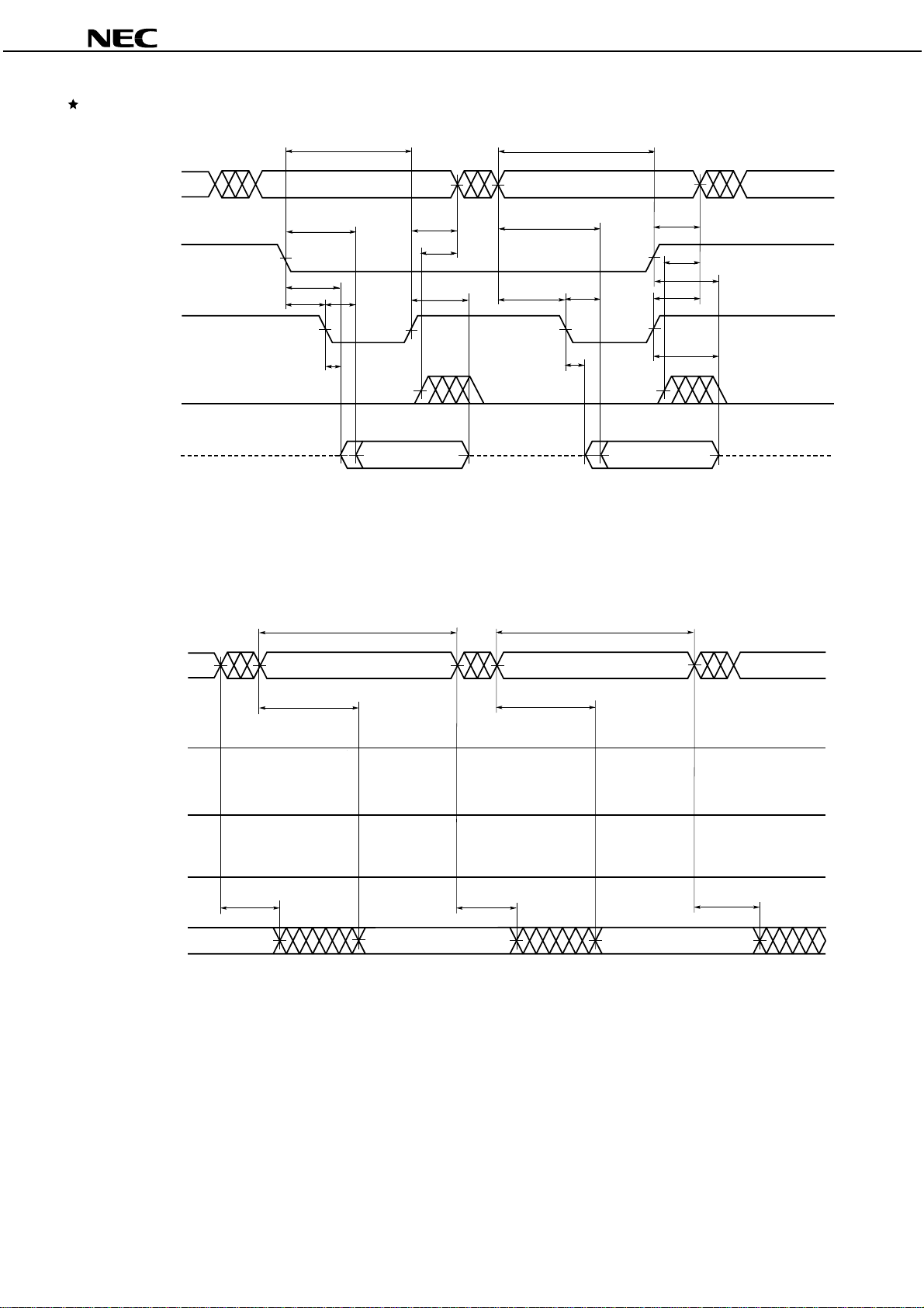
Figure 6-3. Read Cycle Timing Chart 3 (/CS, /OE Controlled)
PD4664312-X
µµµµ
tRC
Address (Input)
/CS (Input)
/OE (Input)
/LB, /UB (Input)
I/O (Output)
tCLZ
tCLOL
High-Z High-Z High-Z
tACS
tOLZ
tOE
A1
tOHAH
tBHAH
tOHZ
Data Out Q1
Remark In read cycle, MODE and /WE should be fixed to high level.
Figure 6-4. Read Cycle Timing Chart 4 (Address Controlled)
tASO
tRC
A2
tAA
tOE
tOLZ
tCHAH
tBHAH
tCHZ
tOHAH
tOHZ
Data Out Q2
A3
t
RC
Address (Input)
/CS (Input)
/OE (Input)
/LB, /UB (Input)
I/O (Output)
t
t
OH
A1
AA
t
OH
Q1
Data Out
Remark In read cycle, MODE and /WE should be fixed to high level.
t
RC
A2
t
AA
t
OH
Data Out Q2
A3
Preliminary Data Sheet M15867EJ5V0DS
21
Page 22
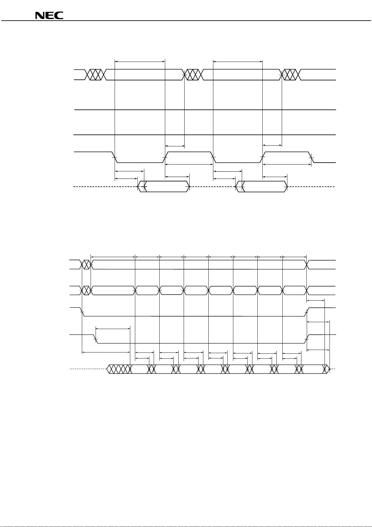
Figure 6-5. Read Cycle Timing Chart 5 (/LB, /UB Controlled)
t
RC
t
RC
PD4664312-X
µµµµ
Address (Input)
A1
/CS (Input)
/OE (Input)
t
BHAH
/LB, /UB (Input)
I/O (Output)
t
BA
t
BLZ
High-Z High-Z High-Z
Data Out Q1
t
BP
t
BHZ
Remark In read cycle, MODE and /WE should be fixed to high level.
Figure 6-6. Page Read Cycle Timing Chart
t
Address
(A3 to A21) (Input)
t
RC
A
N
PRC
A
N+1
t
PRC
A
N+2
t
PRC
A
N+3
A2
t
BHAH
t
BP
t
BA
t
BLZ
t
BHZ
A3
Data Out Q2
t
PRC
A
N+4
t
PRC
A
N+5
t
PRC
A
N+6
t
PRC
A
N+7
Page Address
(A0 to A2) (Input)
/CS (Input)
t
OE
/OE (Input)
t
I/O (Output)
High-Z
ACS
t
PAA
t
OH
Q
N
t
PAA
t
OH
Q
N+1
t
PAA
t
OH
Q
N+2
Q
N+3
Remarks 1. In read cycle, MODE and /WE should be fixed to high level.
2. /LB and /UB are low level.
t
OH
t
CHZ
t
t
PAA
t
OH
t
PAA
t
OH
Q
N+4
t
PAA
t
OH
Q
N+5
t
PAA
t
OH
Q
N+6
OHZ
Q
N+7
22
Preliminary Data Sheet M15867EJ5V0DS
Page 23

Figure 6-7. Write Cycle Timing Chart 1 (/CS Controlled)
t
WC
t
WC
PD4664312-X
µµµµ
Address (Input)
A1
t
t
AS
t
CW
t
WR
AS
A2
t
CW
t
WR
A3
t
AS
/CS (Input)
t
CP
t
CP
/WE (Input)
/LB, /UB (Input)
t
OHAH
t
OES
t
OEH
t
ASO
/OE (Input)
t
I/O (Input)
DW
High-Z High-Z High-Z
t
DH
t
DW
t
DH
Data In D2Data In D1
Cautions 1. During address transition, at least one of pins /CS and /WE, or both of /LB and /UB pins should be
inactivated.
2. Do not input data to the I/O pins while they are in the output state.
3. In write cycle, MODE and /OE should be fixed to high level.
Remark Write operation is done during the overlap time of a low level /CS, /WE, /LB and/or /UB.
Preliminary Data Sheet M15867EJ5V0DS
23
Page 24

Figure 6-8. Write Cycle Timing Chart 2 (/WE Controlled)
PD4664312-X
µµµµ
Address (Input)
/CS (Input)
/WE (Input)
/LB, /UB (Input)
/OE (Input)
I/O (Input)
tOHAH
tWC
A1
tWR
tCHAH
tBHAH
tCP
tWHP
tAS
tCW
tAS
tOES
High-Z High-Z High-Z
tWP tWP
tDW tDH tDW tDH
Data In D1
tCW
tWC
A2
A3
tCHAH
tWR tCP
tBHAH
tASO
tOEH
Data In D2
Cautions 1. During address transition, at least one of pins /CS and /WE, or both of /LB and /UB pins should be
inactivated.
2. Do not input data to the I/O pins while they are in the output state.
3. In write cycle, MODE and /OE should be fixed to high level.
Remark Write operation is done during the overlap time of a low level /CS, /WE, /LB and/or /UB.
24
Preliminary Data Sheet M15867EJ5V0DS
Page 25
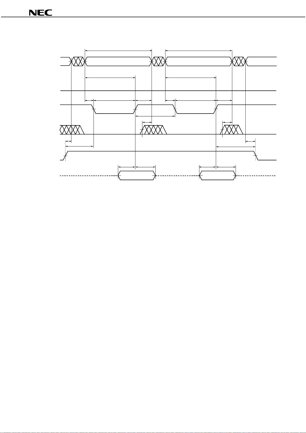
Figure 6-9. Write Cycle Timing Chart 3 (/WE Controlled)
t
WC
t
WC
PD4664312-X
µµµµ
Address (Input)
A1
t
AW
A2
t
AW
A3
/CS (Input)
t
/WE (Input)
AS
t
WP
t
WR
t
t
BHAH
WHP
t
AS
t
WP
t
WR
t
BHAH
/LB, /UB (Input)
t
OHAH
t
OES
t
OEH
t
ASO
/OE (Input)
t
I/O (Input)
DW
High-Z High-Z High-Z
Data In D1
t
DH
t
DW
t
DH
Data In D2
Cautions 1. During address transition, at least one of pins /CS and /WE, or both of /LB and /UB pins should be
inactivated.
2. Do not input data to the I/O pins while they are in the output state.
3. In write cycle, MODE and /OE should be fixed to high level.
Remark Write operation is done during the overlap time of a low level /CS, /WE, /LB and/or /UB.
Preliminary Data Sheet M15867EJ5V0DS
25
Page 26

Figure 6-10. Write Cycle Timing Chart 4 (/LB, /UB Controlled)
t
WC
t
WC
PD4664312-X
µµµµ
Address (Input)
A1
A2
A3
/CS (Input)
/WE (Input)
t
/LB, /UB (Input)
t
OHAH
t
t
t
AS
BW
t
WR
t
t
OES
AS
BP
BW
t
WR
t
BP
t
ASO
t
OEH
/OE (Input)
t
I/O (Input)
DW
High-Z High-Z High-Z
Data In D1
t
DH
t
DW
t
DH
Data In D2
Cautions 1. During address transition, at least one of pins /CS and /WE, or both of /LB and /UB pins should be
inactivated.
2. Do not input data to the I/O pins while they are in the output state.
3. In write cycle, MODE and /OE should be fixed to high level.
Remark Write operation is done during the overlap time of a low level /CS, /WE, /LB and/or /UB.
26
Preliminary Data Sheet M15867EJ5V0DS
Page 27

Figure 6-11. Write Cycle Timing Chart 5 (/LB, /UB Independent Controlled)
t
WC
t
WC
PD4664312-X
µµµµ
Address (Input)
/CS (Input)
/WE (Input)
/LB (Input)
/UB (Input)
/OE (Input)
I/O0 to I/O7 (Input)
t
OHAH
A1
DW
Data In
t
WR
t
AS
t
BP
t
DH
D1
t
AS
t
OES
t
BW
t
High-Z High-Z
A2
t
t
BW
WR
t
OEH
A3
t
ASO
t
DW
I/O8 to I/O15 (Input)
Data In D2
t
DH
High-ZHigh-Z
Cautions 1. During address transition, at least one of pins /CS and /WE, or both of /LB and /UB pins should be
inactivated.
2. Do not input data to the I/O pins while they are in the output state.
3. In write cycle, MODE and /OE should be fixed to high level.
Remark Write operation is done during the overlap time of a low level /CS, /WE, /LB and/or /UB.
Preliminary Data Sheet M15867EJ5V0DS
27
Page 28
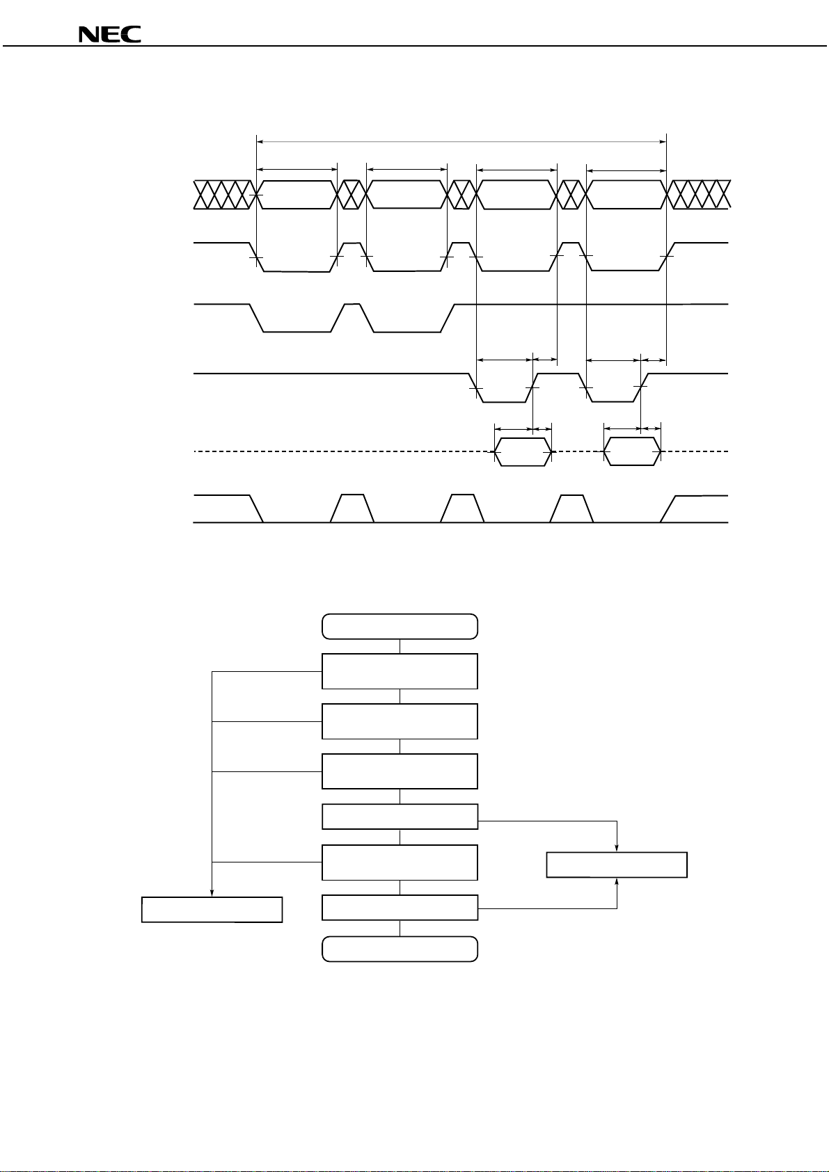
Figure 6-12. Mode Register Setting Timing Chart
Mode Register Setting
t
RC
t
RC
t
WC
PD4664312-X
µµµµ
t
WC
Address (Input)
/CS (Input)
/OE (Input)
/WE (Input)
I/O (Input)
/LB, /UB (Input)
3FFFFFH
3FFFFFH
3FFFFFH
t
WP
tDWt
High-Z High-Z High-Z
xxxxH xxxxH
Figure 6-13. Mode Register Setting Flow Chart
3FFFFFH
t
WR
DH
t
WP
tDWt
t
WR
DH
Mode register setting exit
Note xxH = 04H, 05H, 06H, 07H
Start
No
No
No
No
Address= 3FFFFFH
Read with toggled the /CS, /OE
Address= 3FFFFFH
Read with toggled the /CS, /OE
Address = 3FFFFFH
Write
Data = 00H?
Address = 3FFFFFH
Write
Data = xxH?
End
Note
No
Fail
No
28
Preliminary Data Sheet M15867EJ5V0DS
Page 29

Figure 6-14. Standby Mode 2 (data hold: 16M bits / 8M bits / 4M bits) Entry / Exit Timing Chart
MODE (Input)
t
CHML
/CS (Input)
t
MHCL1
PD4664312-X
µµµµ
MODE (Input)
/CS (Input)
Standby
mode 1
(Data hold: 16M bits / 8M bits / 4M bits)
Standby mode 2
Figure 6-15. Standby Mode 2 (data not held) Entry / Exit Timing Chart
t
CHML
Standby
mode 1
Standby mode 2
(Data not held)
t
MHCL2
Preliminary Data Sheet M15867EJ5V0DS
29
Page 30

7. Package Drawing
93-PIN TAPE FBGA (12x9)
PD4664312-X
µµµµ
INDEX MARK
yS
E
y1 S
φφ
M
SwB
D
SwA
A
A2
e
A1
SxbAB
ZD ZE
A
S
B
CBADEFGHJKLMNP
ITEM MILLIMETERS
D
9.0±0.1
E
12.0±0.1
w
0.2
e
0.8
A
1.3±0.1
0.16±0.05
A1
A2
1.14
b
0.40±0.05
0.08
x
0.1
y
0.2
y1
0.9
ZD
0.8
ZE
P93F9-80-CR2
10
9
8
7
6
5
4
3
2
1
30
Preliminary Data Sheet M15867EJ5V0DS
Page 31

8. Recommended Soldering Conditions
Please consult with our sales offices for soldering conditions of the µPD4664312-X.
Type of Surface Mount Device
PD4664312F9-CR2: 93-pin TAPE FBGA (12 x 9)
µ
PD4664312-X
µµµµ
Preliminary Data Sheet M15867EJ5V0DS
31
Page 32

PD4664312-X
µµµµ
9. Revision History
Edition/ Page Type of Location Description
Date This Previous revision (Previous edition → This edition)
edition edition
5th edition/ Throughout Throughout Deletion Class -C75X, -C85X, -E85X, -E10X,
Aug. 2002 -BE85X, -CE80X, -CE90X
Modification Supply Voltage (Chip) 2.6 to 3.1 V → 2.7 to 3.1 V
p.1 p.1 Deletion Features Fast access time: 80, 85, 90, 100 ns
Fast page access time: 30, 35 ns
pp.1, 15 pp.1, 15 Modification Operating supply current -BE75X: TBD → 40 mA
p.17 pp.17, 18 Addition Read Cycle tOP (MIN.): 2ns
p.20 p.22 Modification Figure 6-2 Timing charts are modified.
p.21 p.23 Modification Figure 6-3 Timing charts are modified.
32
Preliminary Data Sheet M15867EJ5V0DS
Page 33

[ MEMO ]
PD4664312-X
µµµµ
Preliminary Data Sheet M15867EJ5V0DS
33
Page 34

[ MEMO ]
PD4664312-X
µµµµ
34
Preliminary Data Sheet M15867EJ5V0DS
Page 35

µµµµ
NOTES FOR CMOS DEVICES
1 PRECAUTION AGAINST ESD FOR SEMICONDUCTORS
Note:
Strong electric field, when exposed to a MOS device, can cause destruction of the gate oxide and
ultimately degrade the device operation. Steps must be taken to stop generation of static electricity
as much as possible, and quickly dissipate it once, when it has occurred. Environmental control
must be adequate. When it is dry, humidifier should be used. It is recommended to avoid using
insulators that easily build static electricity. Semiconductor devices must be stored and transported
in an anti-static container, static shielding bag or conductive material. All test and measurement
tools including work bench and floor should be grounded. The operator should be grounded using
wrist strap. Semiconductor devices must not be touched with bare hands. Similar precautions need
to be taken for PW boards with semiconductor devices on it.
2 HANDLING OF UNUSED INPUT PINS FOR CMOS
Note:
No connection for CMOS device inputs can be cause of malfunction. If no connection is provided
to the input pins, it is possible that an internal input level may be generated due to noise, etc., hence
causing malfunction. CMOS devices behave differently than Bipolar or NMOS devices. Input levels
of CMOS devices must be fixed high or low by using a pull-up or pull-down circuitry. Each unused
DD
pin should be connected to V
being an output pin. All handling related to the unused pins must be judged device by device and
related specifications governing the devices.
or GND with a resistor, if it is considered to have a possibility of
PD4664312-X
3 STATUS BEFORE INITIALIZATION OF MOS DEVICES
Note:
Power-on does not necessarily define initial status of MOS device. Production process of MOS
does not define the initial operation status of the device. Immediately after the power source is
turned ON, the devices with reset function have not yet been initialized. Hence, power-on does
not guarantee out-pin levels, I/O settings or contents of registers. Device is not initialized until the
reset signal is received. Reset operation must be executed immediately after power-on for devices
having reset function.
Preliminary Data Sheet M15867EJ5V0DS
35
Page 36

PD4664312-X
µµµµ
•
The information in this document is current as of August, 2002. The information is subject to
change without notice. For actual design-in, refer to the latest publications of NEC's data sheets or
data books, etc., for the most up-to-date specifications of NEC semiconductor products. Not all
products and/or types are available in every country. Please check with an NEC sales representative
for availability and additional information.
•
No part of this document may be copied or reproduced in any form or by any means without prior
written consent of NEC. NEC assumes no responsibility for any errors that may appear in this document.
•
NEC does not assume any liability for infringement of patents, copyrights or other intellectual property rights of
third parties by or arising from the use of NEC semiconductor products listed in this document or any other
liability arising from the use of such products. No license, express, implied or otherwise, is granted under any
patents, copyrights or other intellectual property rights of NEC or others.
•
Descriptions of circuits, software and other related information in this document are provided for illustrative
purposes in semiconductor product operation and application examples. The incorporation of these
circuits, software and information in the design of customer's equipment shall be done under the full
responsibility of customer. NEC assumes no responsibility for any losses incurred by customers or third
parties arising from the use of these circuits, software and information.
•
While NEC endeavours to enhance the quality, reliability and safety of NEC semiconductor products, customers
agree and acknowledge that the possibility of defects thereof cannot be eliminated entirely. To minimize
risks of damage to property or injury (including death) to persons arising from defects in NEC
semiconductor products, customers must incorporate sufficient safety measures in their design, such as
redundancy, fire-containment, and anti-failure features.
•
NEC semiconductor products are classified into the following three quality grades:
"Standard", "Special" and "Specific". The "Specific" quality grade applies only to semiconductor products
developed based on a customer-designated "quality assurance program" for a specific application. The
recommended applications of a semiconductor product depend on its quality grade, as indicated below.
Customers must check the quality grade of each semiconductor product before using it in a particular
application.
"Standard": Computers, office equipment, communications equipment, test and measurement equipment, audio
and visual equipment, home electronic appliances, machine tools, personal electronic equipment
and industrial robots
"Special": Transportation equipment (automobiles, trains, ships, etc.), traffic control systems, anti-disaster
systems, anti-crime systems, safety equipment and medical equipment (not specifically designed
for life support)
"Specific": Aircraft, aerospace equipment, submersible repeaters, nuclear reactor control systems, life
support systems and medical equipment for life support, etc.
The quality grade of NEC semiconductor products is "Standard" unless otherwise expressly specified in NEC's
data sheets or data books, etc. If customers wish to use NEC semiconductor products in applications not
intended by NEC, they must contact an NEC sales representative in advance to determine NEC's willingness
to support a given application.
(Note)
(1) "NEC" as used in this statement means NEC Corporation and also includes its majority-owned subsidiaries.
(2) "NEC semiconductor products" means any semiconductor product developed or manufactured by or for
NEC (as defined above).
M8E 00. 4
 Loading...