

DATA SHEET
MOS INTEGRATED CIRCUIT
µ
PD17P709A
4-BIT SINGLE-CHIP MICROCONTROLLER
WITH DEDICATED HARDWARE FOR DIGITAL TUNING SYSTEM
DESCRIPTION
The µPD17P709A is produced by replacing the on-chip mask ROM of the µPD17704A, 17705A, 17707A, 17708A,
and 17709A with a one-time PROM.
µ
PD17P709A allows programs to be written once, so the µPD17P709A is suitable for preproduction in
The
µ
PD17704A, 17705A, 17707A, 17708A, or 17709A system development or low-volume production.
When reading this document, also refer to the publications on the µPD17704A, 17705A, 17707A, 17708A,
or 17709A.
The electrical characteristics (including power supply current) and PLL analog characteristics of the
µ
PD17P709A differ from those of the µPD17704A, 17705A, 17707A, 17708A, and 17709A. In high-volume
application set production, be sure to carefully check these differences.
FEATURES
• Compatible with the
• On-chip one-time PROM: 32 KB (16384 × 16 bits)
• Supply voltage: VDD = 5 V ±10%
ORDERING INFORMATION
Part Number Package
µ
PD17P709AGC-3B9 80-pin plastic QFP (14 × 14)
µ
PD17704A, 17705A, 17707A, 17708A, and 17709A
The information in this document is subject to change without notice. Before using this document, please
confirm that this is the latest version.
Not all devices/types available in every country. Please check with local NEC representative for
availability and additional information.
Document No. U15723EJ1V0DS00 (1st edition)
Date Published October 2001 N CP(K)
Printed in Japan
©
2001
FUNCTIONAL OUTLINE
Part Number
Item
Program memory (ROM)
General-purpose data memory (RAM)
Instruction execution time 1.78 µs (with fX = 4.5 MHz crystal oscillator)
General-purpose ports • I/O ports: 46
Stack levels • Address stack: 15 levels
Interrupts • External: 6 sources (falling edge of CE pin, INT0 to INT4)
Timer 5 channels
A/D converter 8 bits × 6 channels (hardware mode and software mode selectable)
D/A converter (PWM) 3 channels (8-bit or 9-bit resolution selectable by software)
Serial interface 2 units (3 channels)
PLL Division mode • Direct division mode (VCOL pin (MF mode): 0.5 to 3 MHz)
Reference frequency
Charge pump Two error-out output pins (EO0, EO1)
Phase comparator Unlock status detectable by program
Intermediate frequency counter • Intermediate frequency (IF) measurement
BEEP output 2 pins
µ
PD17704AµPD17705AµPD17707AµPD17708AµPD17709AµPD17P709A
8192 × 16 bits
(mask ROM) (mask ROM) (mask ROM)
672 × 4 bits 1120 × 4 bits 1176 × 4 bits
• Input ports: 12
• Output ports: 4
• Interrupt stack: 4 levels
• DBF stack: 4 levels (can be manipulated via software)
• Internal: 6 sources (timers 0 to 3, serial interfaces 0 and 1)
• Basic timer (clock: 10, 20, 50, 100 Hz): 1 channel
• 8-bit timer with gate counter (clock: 1 k, 2 k, 10 k, 100 kHz): 1 channel
• 8-bit timer (clock: 1 kHz, 2 kHz, 10 kHz, 100 kHz): 2 channels
• 8-bit timer multiplexed with PWM (clock: 440 Hz, 4.4 kHz): 1 channel
Output frequency: 4.4 kHz, 440 Hz (with 8-bit PWM selected)
• 3-wire serial I/O: 2 channels
• 2-wire serial I/O/I2C bus: 1 channel
• Pulse swallow mode (VCOL pin (HF mode): 10 to 40 MHz)
13 types selectable (1, 1.25, 2.5, 3, 5, 6.25, 9, 10, 12.5, 18, 20, 25, 50 kHz)
P1C0/FMIFC pin: 10 to 11 MHz in FMIF mode
P1C1/AMIFC pin: 0.4 to 0.5 MHz in AMIF mode
• External gate width measurement
P2A1/FCG1, P2A0/FCG0 pin
Output frequency: 1 kHz, 3 kHz, 4 kHz, 6.7 kHz (BEEP0 pin)
12288 × 16 bits 16384 × 16 bits
2.2 kHz, 220 Hz (with 9-bit PWM selected)
(VCOH pin (VHF mode): 60 to 130 MHz)
0.4 to 0.5 MHz in AMIF mode
67 Hz, 200 Hz, 3 kHz, 4 kHz (BEEP1 pin)
µ
PD17P709A
(1/2)
16384 × 16 bits
(one-time PROM)
2
Data Sheet U15723EJ1V0DS
Part Number
Item
Reset • Power-on reset (on power application)
Standby • Clock stop mode (STOP)
Supply voltage • PLL operation: VDD = 4.5 to 5.5 V
Package 80-pin plastic QFP (14 × 14)
µ
PD17704AµPD17705AµPD17707AµPD17708AµPD17709AµPD17P709A
• Reset by RESET pin
• Watchdog timer reset
Can be set only once on power application: 65536 instructions, 131072
• Stack pointer overflow/underflow reset
Can be set only once on power application: interrupt stack or address stack
• CE reset (CE pin low → high level)
CE reset delay timing can be set.
• Power failure detection function
• Halt mode (HALT)
• CPU operation: VDD = 3.5 to 5.5 V
µ
PD17P709A
instructions, or no-use
selectable
selectable
(2/2)
Data Sheet U15723EJ1V0DS
3
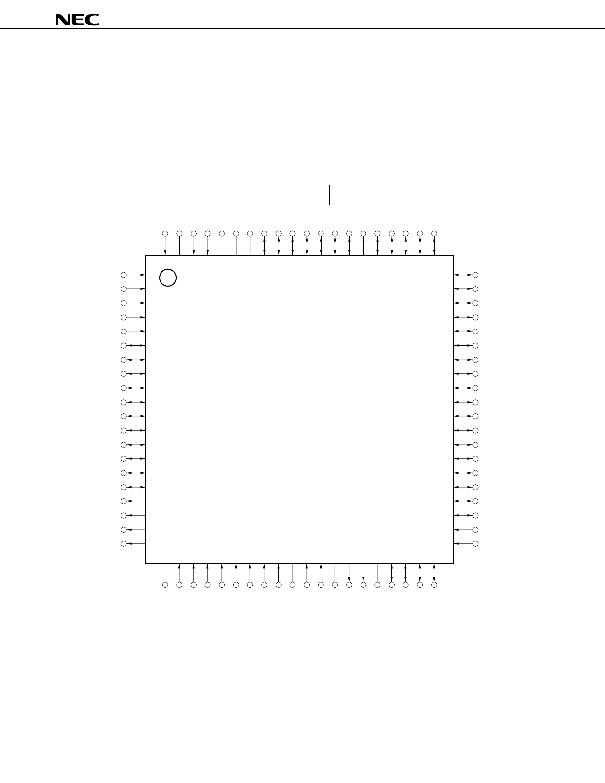
PIN CONFIGURATION (TOP VIEW)
80-pin plastic QFP (14 × 14)
µ
PD17P709AGC-3B9
(1) Normal operation mode
0
DD
INXOUT
CE
X
V
INT2
P1A3/INT4
P1A2/INT3
P1A1
P1A0/TM0G
P3A3
P3A2
P3A1
P3A0
P3B3
P3B2
P3B1
P3B0
P2A2
P2A1/FCG1
P2A0/FCG0
P1B3
P1B2/PWM2
P1B1/PWM1
P1B0/PWM0
RESET
80 79 78 77 76 75 74 73 72 71 70 69 68 67 66 65 64 63 62 61
1
2
3
4
5
6
7
8
9
10
11
12
13
14
15
16
17
18
19
20
22
21 23 24 25 26 27 28 29 30 31 32 33 34 35 36 37 38 39 40
GND0
REG
P2D0
P2D1
P2D2
P0B0/SI1
P0B1/SO1
P0B2/SCK1
P0B3/SI0
P0A0/SO0
P0A1/SCK0
P0A2/SCL
P0A3/SDA
P0C0
P0C1
60
59
58
57
56
55
54
53
52
51
50
49
48
47
46
45
44
43
42
41
µ
PD17P709A
P0C2
P0C3
P2C0
P2C1
P2C2
P2C3
P3D0
P3D1
P3D2
P3D3
P3C0
P3C1
P3C2
P3C3
P2B0
P2B1
P2B2
P2B3
INT0
INT1
1
DD
GND2
P0D3/AD3
P0D2/AD2
P0D1/AD1
P0D0/AD0
P1C3/AD5
P1C2/AD4
4
Data Sheet U15723EJ1V0DS
V
P1C0/FMIFC
P1C1/AMIFC
VCOH
VCOL
GND1
EO0
EO1
TEST
P1D3
P1D2
P1D1/BEEP1
P1D0/BEEP0
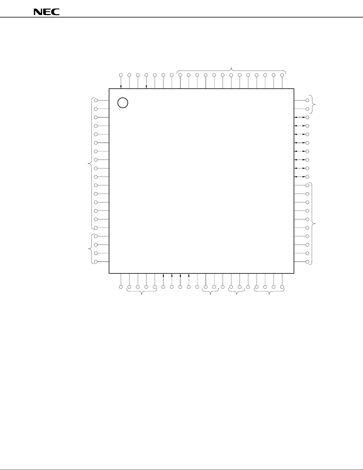
(2) PROM programming mode
µ
PD17P709A
(L)
(OPEN)
(OPEN)
GND0
Note
(L)
REG
0
DD
(L)
(H)
80 79 78 77 76 75 74 73 72 71 70 69 68 67 66 65 64 63 62 61
1
2
3
4
5
6
7
8
9
10
11
12
13
14
15
16
17
18
19
20
21 22 23 24 25 26 27 28 29 30 31 32 33 34 35 36 37 38 39 40
CLK
V
60
59
58
57
56
55
54
53
52
51
50
49
48
47
46
45
44
43
42
41
(L)
D0
D1
D2
D3
D4
D5
D6
D7
(L)
GND2
(L)
Note Connect to the same potential as V
MD3
DD.
MD2
MD1
MD0
1
DD
V
(L)
GND1
(OPEN)
PP
V
(L)
Caution The items in parentheses indicate the processing of pins not used in the PROM programming
mode.
L: Independently connect to GND via a resistor (470 Ω)
H: Independently connect each pin to VDD via a resistor (470 Ω)
OPEN: Leave open.
Data Sheet U15723EJ1V0DS
5

PIN NAMES
µ
PD17P709A
AD0 to AD5: A/D converter input
AMIFC: AM frequency counter input
BEEP0, BEEP1: BEEP output
CE: Chip enable
CLK: Address update clock input
D0 to D7: Data I/O
EO0, EO1: Error-out output
FCG0, FGC1: Frequency counter gate input
FMIFC: FM frequency counter input
GND0 to GND2: Ground 0 to 2
INT0 to INT4: External interrupt input
MD0 to MD3: Operation mode selection
PWM0 to PWM2: D/A converter output
P0A0 to P0A3: Port 0A
P0B0 to P0B3: Port 0B
P0C0 to P0C3: Port 0C
P0D0 to P0D3: Port 0D
P1A0 to P1A3: Port 1A
P1B0 to P1B3: Port 1B
P1C0 to P1C3: Port 1C
P1D0 to P1D3: Port 1D
P2A0 to P2A2: Port 2A
P2B0 to P2B3: Port 2B
P2C0 to P2C3: Port 2C
P2D0 to P2D2: Port 2D
P3A0 to P3A3: Port 3A
P3B0 to P3B3: Port 3B
P3C0 to P3C3: Port 3C
P3D0 to P3D3: Port 3D
REG: CPU regulator
RESET: Reset input
SCK0, SCK1: 3-wire serial clock I/O
SCL: 2-wire serial clock I/O
SDA: 2-wire serial data I/O
SI0, SI1: 3-wire serial data input
SO0, SO1: 3-wire serial data output
TEST: Test input
TM0G: Timer 0 gate input
VCOH: Local oscillation high input
VCOL: Local oscillation low input
DD0, VDD1: Power supply
V
VPP: Program voltage application
XIN, XOUT: Main clock oscillation
6
Data Sheet U15723EJ1V0DS
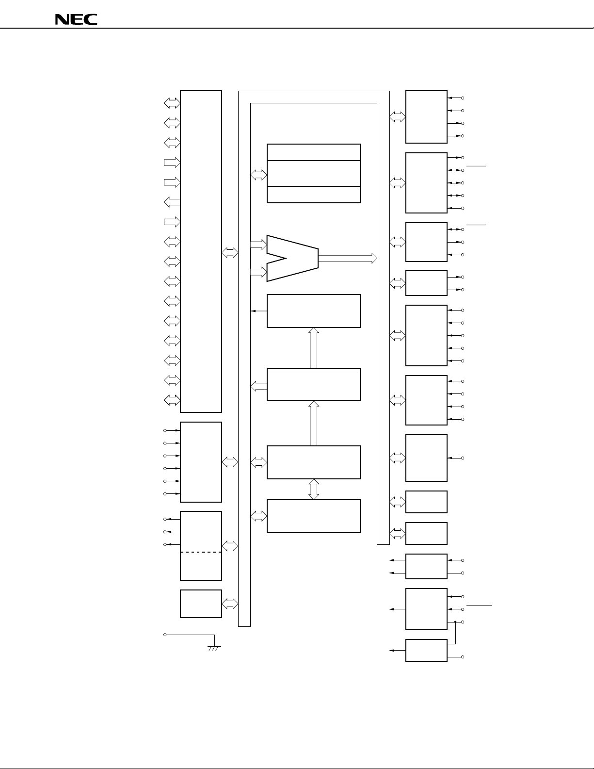
BLOCK DIAGRAM
µ
PD17P709A
P0A0 to P0A3
P0B0 to P0B3
P0C0 to P0C3
P0D0 to P0D3
P1A0 to P1A3
P1B0 to P1B3
P1C0 (MD0)
to P1C3 (MD3)
P1D0 to P1D3
P2A0 to P2A2
P2B0 to P2B3
P2C0 (D0)
to P2C3 (D3)
P2D0 to P2D2
P3A0 to P3A3
P3B0 to P3B3
P3C0 to P3C3
P3D0 (D4)
to P3D3 (D7)
AD0/P0D0
AD1/P0D1
AD2/P0D2
AD3/P0D3
AD4/P1C2
AD5/P1C3
PWM0/P1B0
PWM1/P1B1
PWM2/P1B2
4
4
4
4
4
4
4
4
3
4
4
3
4
4
4
4
Ports
A/D
converter
D/A
converter
8-bit
timer 3
RF
RAM
1776 × 4 bits
SYSREG
ALU
Instruction
decoder
One-time PROM
16384 × 16 bits
Program counter
Stack
CPU
Peripheral
PLL
Serial
interface 0
Serial
interface 1
BEEP
Interrupt
control
Frequency
counter
8-bit
timer 0
gate
counter
8-bit
timer 1
8-bit
timer 2
OSC
VCOH
VCOL
EO0
EO1
SO0/P0A0
SCK0/P0A1
SCL/P0A2
SDA/P0A3
SI0/P0B3
SCK1/P0B2
SO1/P0B1
SI1/P0B0
BEEP0/P1D0
BEEP1/P1D1
INT0
INT1
INT2
INT3/P1A2
INT4/P1A3
FCG0/P2A0
FCG1/P2A1
FMIFC/P1C0
AMIFC/P1C1
TM0G/P1A0
X
IN
X
OUT
Basic
timer
GND0 to GND2
V
CPU
Remark Pins in parentheses are used in PROM programming mode.
Data Sheet U15723EJ1V0DS
Reset
Regulator
CE
RESET
V
DD
0, VDD1
REG
7

µ
PD17P709A
CONTENTS
1. PIN FUNCTIONS .............................................................................................................................. 9
1.1 Pin Function List .................................................................................................................. 9
1.2 PROM Programming Mode ................................................................................................. 13
1.3 Equivalent Circuits of Pins ................................................................................................. 14
1.4 Connections of Unused Pins .............................................................................................. 19
1.5 Cautions on Using CE, INT0 to INT4, and RESET Pins
(Only in Normal Operation Mode) ...................................................................................... 21
1.6 Cautions on Using TEST Pin (Only in Normal Operation Mode) ..................................... 21
2. ONE-TIME PROM (PROGRAM MEMORY) WRITE, READ, AND VERIFY .................................... 22
2.1 Operation Modes for Program Memory Write, Read and Verify ...................................... 23
2.2 Program Memory Write Procedure .................................................................................... 24
2.3 Program Memory Read Procedure ..................................................................................... 25
3. ELECTRICAL SPECIFICATIONS .........................................................................................................26
4. PACKAGE DRAWING ..........................................................................................................................31
5. RECOMMENDED SOLDERING CONDITIONS ...................................................................................32
APPENDIX DEVELOPMENT TOOLS ......................................................................................................33
8
Data Sheet U15723EJ1V0DS
µ
PD17P709A
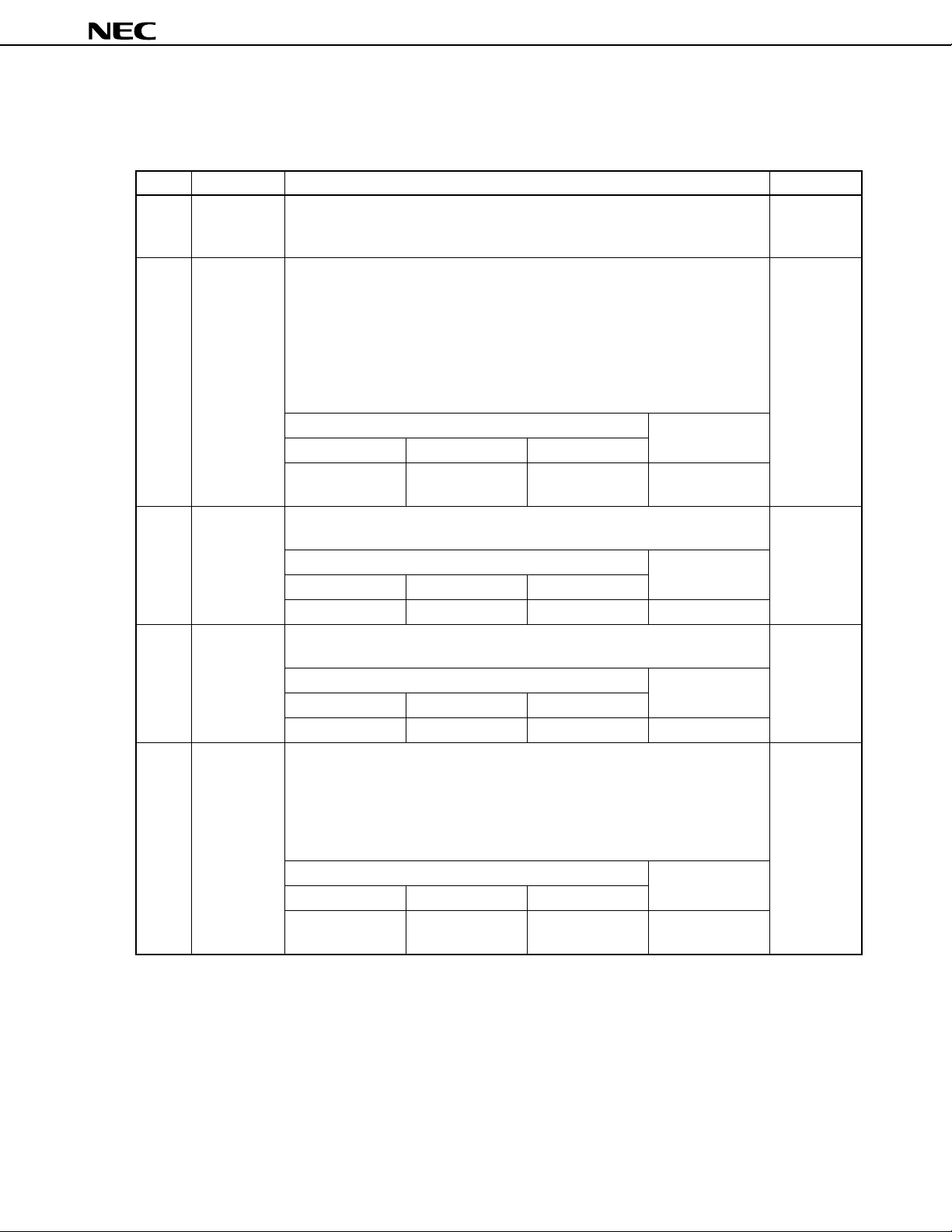
1. PIN FUNCTIONS
1.1 Pin Function List
Pin No. Symbol Function Output Form
1 INT2 Edge-detectable vectored interrupt input pins. Rising or falling edge can be –
41 INT1 specified.
42 INT0
2 P1A3/INT4 Port 1A multiplexed with external interrupt request signal input and event –
3 P1A2/INT3 signal input pins.
4 P1A1 • P1A3 to P1A0
5 P1A0/TM0G • 4-bit input port
• INT4, INT3
• Edge-detectable vectored interrupt
• TM0G
• Input for gate of 8-bit timer 0
After reset
Power-on reset WDT&SP reset CE reset
Input Input Retained Retained
(P1A3 to P1A0) (P1A3 to P1A0)
6 P3A3 4-bit I/O port. CMOS
| | Input or output can be specified in 4-bit units. push-pull
9 P3A0
Power-on reset WDT&SP reset CE reset
Input Input Retained Retained
10 P3B3 4-bit I/O port. CMOS
| | Input or output can be specified in 4-bit units. push-pull
13 P3B0
Power-on reset WDT&SP reset CE reset
Input Input Retained Retained
14 P2A2 Port 2A multiplexed with external gate counter input pins. CMOS
15 P2A1/FCG1 • P2A2 to P2A0 push-pull
16 P2A0/FCG0 • 3-bit I/O port
• Input or output can be specified in 1-bit units.
• FCG1, FCG0
• Input for external gate counter
Power-on reset WDT&SP reset CE reset
Input Input Retained Retained
(P2A2 to P2A0) (P2A2 to P2A0) (P2A2 to P2A0) (P2A2 to P2A0)
After reset
After reset
After reset
With clock stopped
With clock stopped
With clock stopped
With clock stopped
Data Sheet U15723EJ1V0DS
9
µ
PD17P709A
Pin No. Symbol Function Output Form
17 P1B3 Port 1B multiplexed with D/A converter output pins. N-ch
18 P1B2/PWM2 • P1B3 to P1B0 open-drain
| | • 4-bit output port (12 V
20 P1B0/PWM0 • PWM2 to P2M0 withstanding
• 8- or 9-bit D/A converter output voltage)
After reset
Power-on reset WDT&SP reset CE reset
Outputs low level Outputs low level Retained Retained
(P1B3 to P1B0) (P1B3 to P1B0) (P1B3 to P1B0)
21 GND2 Ground –
33 GND1
75 GND0
22 P0D3/AD3 Port 0D multiplexed with A/D converter input pins –
| | • P0D3 to P0D0
25 P0D0/AD0 • 4-bit input port
• Pull-down resistors can be connected in 1-bit units.
• AD3 to AD0
• Analog input of A/D converter with 8-bit resolution
After reset
Power-on reset WDT&SP reset CE reset
Input with pull-down Input with pull-down
resistor resistor
(P0D3 to P0D0) (P0D3 to P0D0)
26 P1C3/AD5 Port 1C multiplexed with A/D converter input and IF counter input pins. –
27 P1C2/AD4 • P1C3 to P1C0
28 P1C1/AMIFC • 4-bit input port
29 P1C0/FMIFC • AD5, AD4
• Analog input to A/D converter with 8-bit resolution
• FMIFC, AMIFC
• Input to frequency counter
After reset
Power-on reset WDT&SP reset CE reset
Input Input • P1C3/AD5, • P1C3/AD5,
(P1C3 to P1C0) (P1C3 to P1C0) P1C2/AD4 P1C2/AD4
Retained Retained
Retained Retained
• P1C1/AMIFC, • P1C1/AMIFC,
P1C0/FMIFC P1C0/FMIFC
Input Input
(P1C1, P1C0) (P1C1, P1C0)
With clock stopped
With clock stopped
With clock stopped
10
Data Sheet U15723EJ1V0DS
µ
PD17P709A
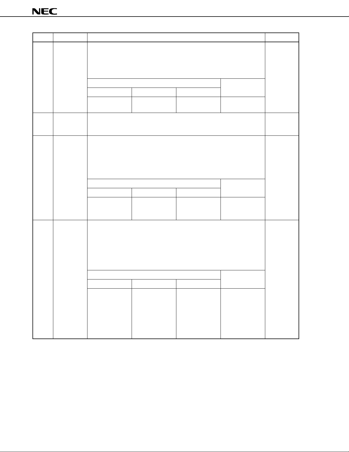
Pin No. Symbol Function Output Form
30 VDD1 Power supply. Supply the same voltage to these pins. –
79 VDD0 • With CPU and peripheral function operating: 4.5 to 5.5 V
• With CPU operating: 3.5 to 5.5 V
• With clock stopped: 2.2 to 5.5 V
31 VCOH PLL local oscillation (VCO) frequency input. –
32 VCOL • VCOH
• Active with VHF mode selected by program; otherwise, pulled down.
• VCOL
•
Active with HF or MW mode selected by program; otherwise, pulled down.
Because the input of these pins goes into an AC amplifier, cut the DC
component of the input signal with a capacitor.
34 EO0 Output from charge pump of PLL frequency synthesizer. Outputs the divided CMOS
35 EO1 frequency of local oscillation and the result of comparison of the phase 3-state
difference of the reference frequency.
After reset
Power-on reset WDT&SP reset CE reset
High-impedance High-impedance High-impendance High-impedance
output output output output
36 TEST Test input pin. –
Be sure to connect this pin to GND.
37 P1D3 Port 1D and BEEP output. CMOS
38 P1D2 • P1D3 to P1D0 push-pull
39 P1D1/BEEP1 • 4-bit I/O port
40 P1D0/BEEP0 • Input or output can be specified in 1-bit units.
• BEEP1, BEEP0
• BEEP output
After reset
Power-on reset WDT&SP reset CE reset
Input Input Retained Retained
(P1D3 to P1D0) (P1D3 to P1D0) (P1D3 to P1D0) (P1D3 to P1D0)
43 P2B3 4-bit I/O port. CMOS
| | Input or output can be specified in 1-bit units. push-pull
46 P2B0
Power-on reset WDT&SP reset CE reset
Input Input Retained Retained
47 P3C3 4-bit I/O port. CMOS
| | Input or output can be specified in 4-bit units. push-pull
50 P3C0
Power-on reset WDT&SP reset CE reset
Input Input Retained Retained
After reset
After reset
With clock stopped
With clock stopped
With clock stopped
With clock stopped
Data Sheet U15723EJ1V0DS
11

µ
PD17P709A
Pin No. Symbol Function Output Form
51 P3D3 4-bit I/O port. CMOS
| | Input or output can be specified in 4-bit units. push-pull
54 P3D0
Power-on reset WDT&SP reset CE reset
Input Input Retained Retained
55 P2C3 4-bit I/O port. CMOS
| | Input or output can be specified in 4-bit units. push-pull
58 P2C0
Power-on reset WDT&SP reset CE reset
Input Input Retained Retained
59 P0C3 4-bit I/O port. CMOS
| | Input or output can be specified in 4-bit units. push-pull
62 P0C0
Power-on reset WDT&SP reset CE reset
Input Input Retained Retained
63 P0A3/DSA Ports P0A and P0B are multiplexed with I/O of serial interface. N-ch
64 P0A2/SCL • P0A3 to P0A0 open-drain
65 P0A1/SCK0
66 P0A0/SO0
67 P0B3/SI0
68 P0B2/SCK1
69 P0B1/SO1
70 P0B0/SI1
71 P2D2 3-bit I/O port. CMOS
| | Input or output can be specified in 1-bit units. push-pull
73 P2D0
• 4-bit I/O port
• Input or output can be specified in 1-bit units.
• P0B3 to P0B0
• 4-bit I/O port
• Input or output can be specified in 1-bit units.
• SDA, SCL
• Serial data and serial clock I/O of serial interface 0 in 2-wire serial I/O or
I2C bus mode
• SCK0, SO0, SI0
•
Serial clock I/O, serial data output, and serial data input of serial interface
0 in 3-wire serial I/O mode
• SCK1, SO1, SI1
• Serial clock I/O, serial data output, serial data input of serial interface 1
in 3-wire serial I/O mode
Power-on reset WDT&SP reset CE reset
Input Input Retained Retained
P0A3 to P0A0, P0A3 to P0A0, P0A3 to P0A0, P0A3 to P0A0,
P0B3 to P0B0 P0B3 to P0B0 P0B3 to P0B0 P0B3 to P0B0
Power-on reset WDT&SP reset CE reset
Input Input Retained Retained
After reset
After reset
After reset
After reset
After reset
With clock stopped
With clock stopped
With clock stopped
CMOS
push-pull
With clock stopped
With clock stopped
12
Data Sheet U15723EJ1V0DS

µ
PD17P709A
Pin No. Symbol Function Output Form
74 REG CPU regulator. –
Connect this pin to GND via 0.1 µF capacitor.
76 X
77 XIN
78 CE Device operation selection, CE reset, and interrupt signal input pin. –
80 RESET Reset input –
OUT Ground pins of crystal resonator. –
• Device operation selection
When CE is high, the PLL frequency synthesizer can operate.
When CE is low, the PLL frequency synthesizer is automatically disabled
internally.
• CE reset
When CE goes high, the device is reset at the rising edge of the internal
basic timer setting pulse. This pin also has a reset timing delay function.
• Interrupt
A vectored interrupt occurs at the falling edge of this pin.
1.2 PROM Programming Mode
Pin No. Symbol Function Output Form
26 MD3 Input for operating mode selection for program memory write, read, or –
| | verify.
29 MD0
21 GND2 Ground –
33 GND1
75 GND0
36 VPP Pin to which program voltage is applied during program memory write, read, –
or verify. +12.5 V is applied.
30 VDD1 Power supply pins. +6 V is applied during program memory write, read, or –
79 VDD0 verify.
51 D7 8-bit data I/O for program memory write, read, or verify
| |
58 D0
77 CLK Clock input for address updating during program memory write, read, or –
verify
CMOS push-pull
Remark The pins other than those listed above are not used in PROM programming mode. For the handling
of the unused pins, see PIN CONFIGURATION (2) PROM programming mode.
Data Sheet U15723EJ1V0DS
13

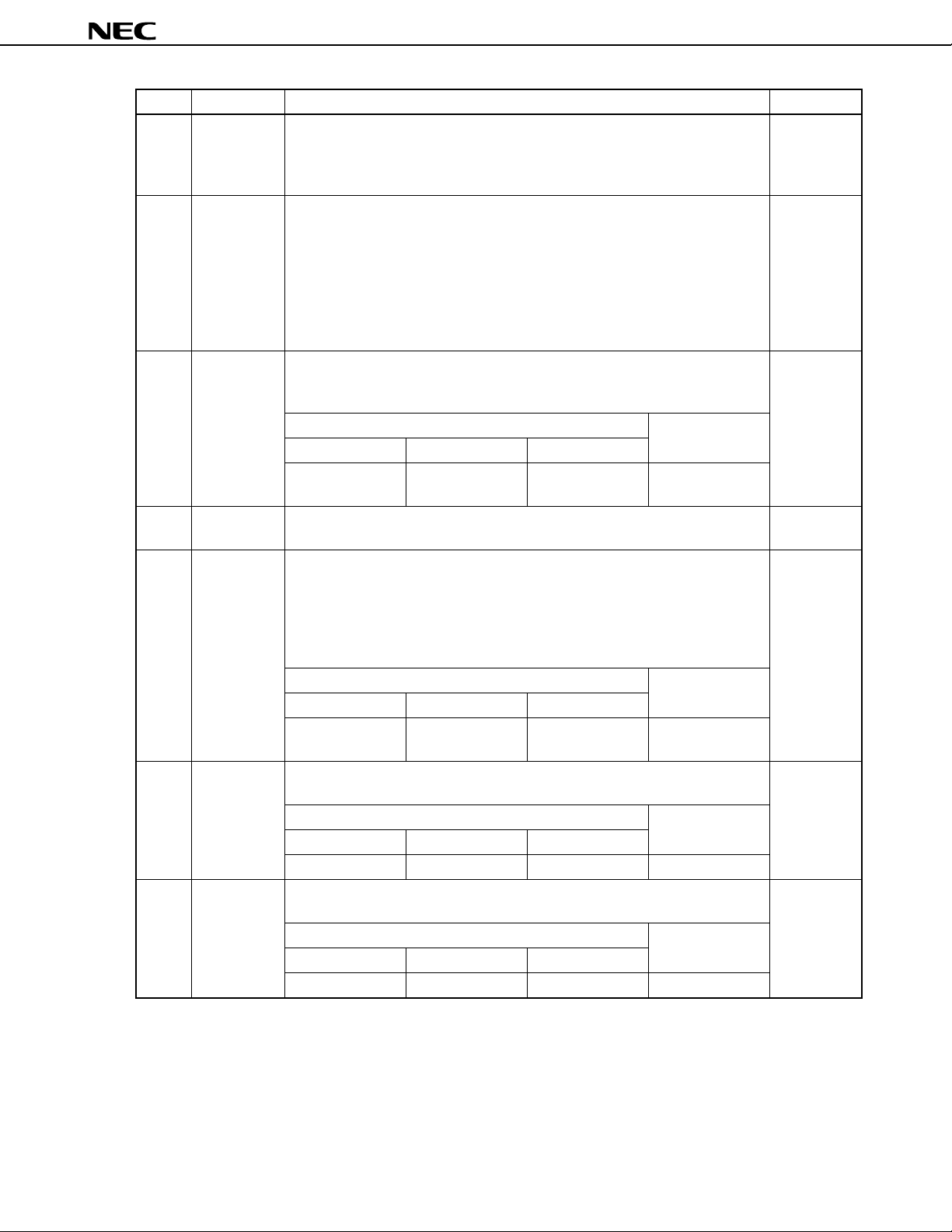
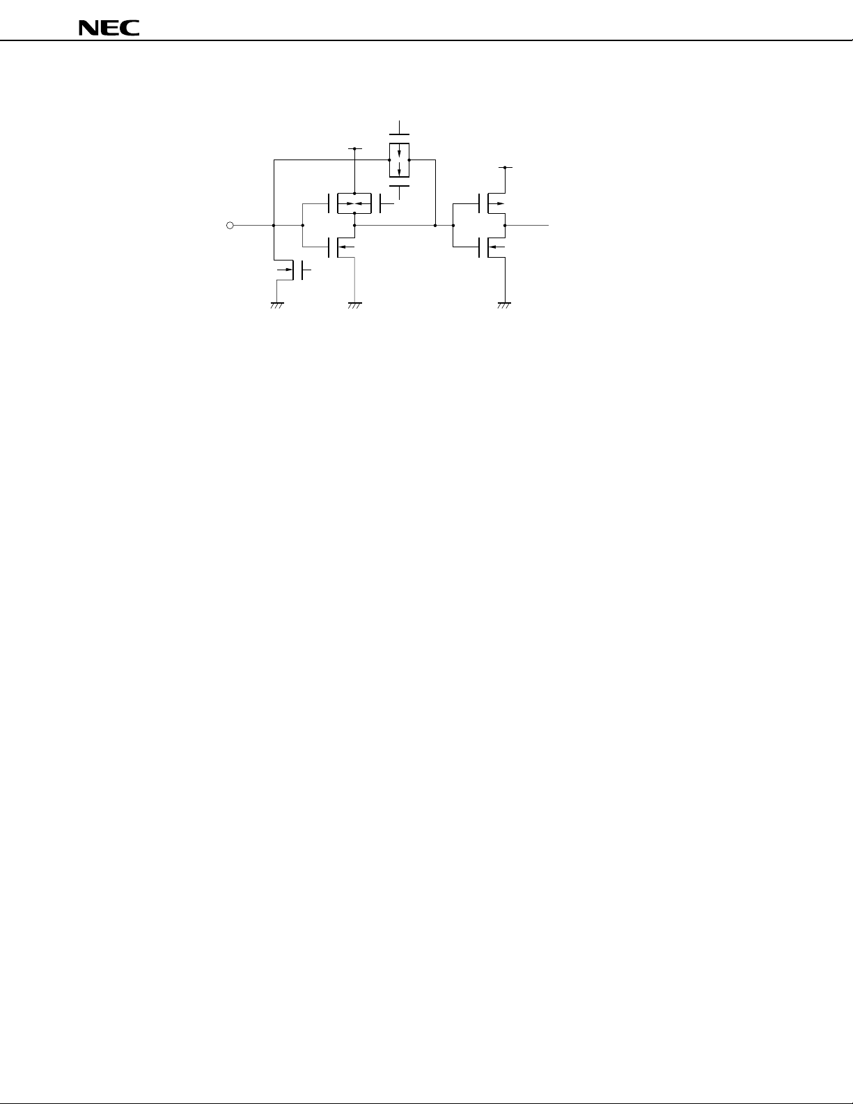
1.3 Equivalent Circuits of Pins
(1) P0A (P0A1/SCK0, P0A0/SO0)
P0B (P0B3/SI0, P0B2/SCK1, P0B1/SO1, P0B0/SI1)
P0C (P0C3, P0C2, P0C1, P0C0)
P1D (P1D3, P1D2, P1D1/BEEP1, P1D0/BEEP0)
P2A (P2A2, P2A1/FCG1, P2A0/FCG0)
P2B (P2B3, P2B2, P2B1, P2B0)
P2C (P2C3, P2C2, P2C1, P2C0)
P2D (P2D2, P2D1, P2D0)
P3A (P3A3, P3A2, P3A1, P3A0)
P3B (P3B3, P3B2, P3B1, P3B0)
P3C (P3C3, P3C2, P3C1, P3C0)
P3D (P3D3, P3D2, P3D1, P3D0)
µ
PD17P709A
(I/O)
V
DD
CKSTOP
V
DD
Note
Note This is an internal signal that is output when the clock stop instruction is executed. Its circuit is
designed not to increase the current consumption due to noise even if it is floated.
14
Data Sheet U15723EJ1V0DS

(2) P0A (P0A3/SDA, P0A2/SCL) (I/O)
µ
PD17P709A
V
DD
CKSTOP
Note
Note This is an internal signal that is output when the clock stop instruction is executed. Its circuit is
designed not to increase the current consumption due to noise even if it is floated.
(3) P1B (P1B3, P1B2/PWM2, P1B1/PWM1, P1B0/PWM0) (output)
(4) P0D (P0D3/AD3, P0D2/AD2, P0D1/AD1, P0D0/AD0) (input)
A/D converter
V
DD
CKSTOP
P0DPLD flag
High on-resistance
Note
Note This is an internal signal that is output when the clock stop instruction is executed. Its circuit is
designed not to increase the current consumption due to noise even if it is floated.
Data Sheet U15723EJ1V0DS
15
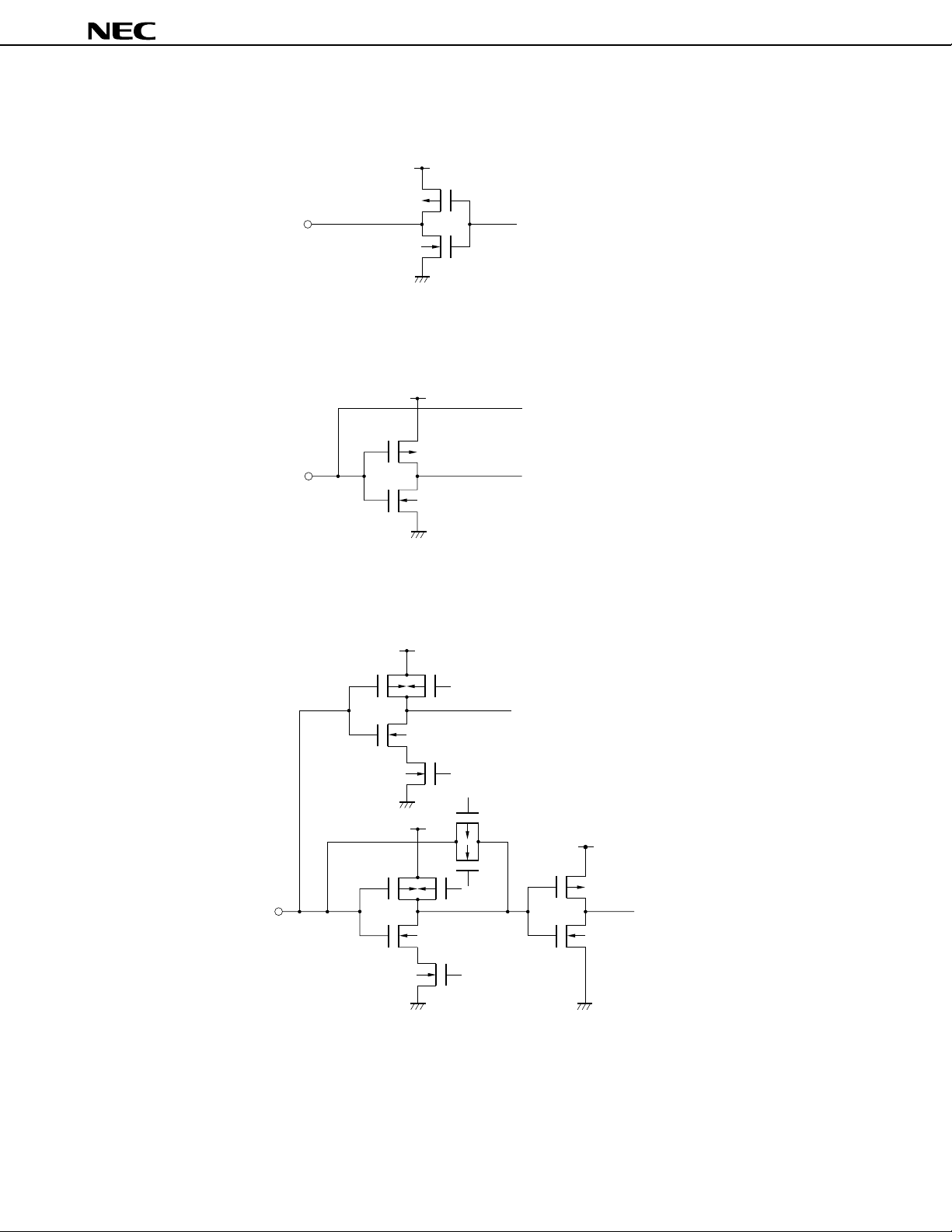
(5) P1A (P1A1) (input)
(6) P1C (P1C3/AD5, P1C2/AD4) (input)
V
VDD
DD
A/D converter
µ
PD17P709A
(7) P1C (P1C1/AMIFC, P1C0/FMIFC) (input)
V
DD
General-purpose port
V
DD
High on-resistance
V
DD
Frequency counter
16
Data Sheet U15723EJ1V0DS
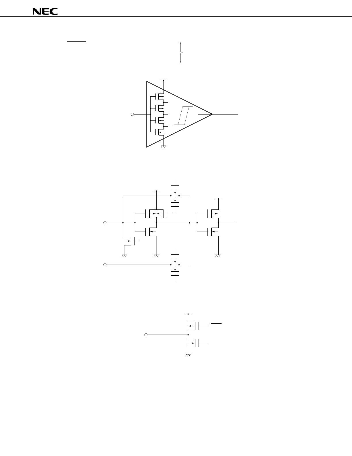
(8) CE
RESET
INT0, INT1, INT2 (Schmitt-triggered input)
P1A (P1A3/INT4, P1A2/INT3, P1A0/TM0G)
VDD
OUT (output), XIN (input)
(9) X
µ
PD17P709A
IN
X
X
OUT
(10) EO1, EO0 (output)
High onresistance
V
DD
High on-resistance
V
V
DD
DWN
UP
DD
Internal clock
Data Sheet U15723EJ1V0DS
17
(11) VCOH, VCOL (input)
µ
PD17P709A
High onresistance
V
DD
High on-resistance
V
DD
18
Data Sheet U15723EJ1V0DS
µ
1.4 Connections of Unused Pins
It is recommended to connect unused pins as follows.
Table 1-1. Connections of Unused Pins
Pin Name I/O Mode Recommended Connection
Port pin P0D3/AD3 to P0D0/AD0 Input Independently connect to GND via a resistor
P1C3/AD5
P1C2/AD4
P1C1/AMIFC
P1C0/FMIFC
P1A3/INT4 Independently connect to GND via a resistor
P1A2/INT3
P1A1
P1A0/TM0G
P1B3 N-ch open-drain Set to low-level output by software and leave open.
P1B2/PWM2 to P1B0/PWM0
P0A3/SDA I/O
P0A2/SCL independently connect to VDD or GND via a resistor
P0A1/SCK0
P0A0/SO0
P0B3/SI0
P0B2/SCK1
P0B1/SO1
P0B0/SI1
P0C3 to P0C0
P1D3
P1D2
P1D1/BEEP1
P1D0/BEEP0
P2A2
P2A1/FCG1
P2A0/FCG0
P2B3 to P2B0
P2C3 to P2C0
P2D2 to P2D0
Note 2
Note 2
output
Note 3
Set to port mode and individually connect to VDD or GND
via a resistor
Set to general-purpose input port mode by software and
Note 1
.
PD17P709A
(1/2)
Note 1
.
Note 1
.
Note 1
.
Notes 1. If a pin is externally pulled up (connected to VDD via a resistor) or pulled down (connected to GND
via a resistor) with a high resistance, the pin almost enters a high-impedance state, increasing the
current (through-current) consumption of the port. Generally, the resistance of a pull-up or pull-
down resistor is several 10 kΩ, although it depends on the application circuit.
2. Do not set these pins as AMIFC and FMIFC pins; otherwise, the current consumption will increase.
3. The I/O ports are set in the general-purpose input port mode at power-on reset, when reset by the
RESET pin, or when reset by an overflow or underflow of the watchdog timer or the stack.
Data Sheet U15723EJ1V0DS
19
µ
PD17P709A
Table 1-1. Connections of Unused Pins
(2/2)
Pin Name I/O Mode Recommended Connection
Port pin P3A3 to P3A0 I/O
P3B3 to P3B0 independently connect to VDD or GND via a resistor
P3C3 to P3C0
P3D3 to P3D0
Non-port CE Input Connect to VDD via a resistor
pins
EO1 Output Leave open.
EO0
INT0 to INT2 Input Independently connect to GND via a resistor
RESET Input Connect to VDD via a resistor
TEST – Directly connect to GND.
VCOH Input Disable PLL via software and leave open.
VCOL
Note 2
Set in general-purpose input port mode by software and
Note 1
Note 1
.
Note 1
.
Note 1
.
Notes 1. If a pin is externally pulled up (connected to VDD via a resistor) or pulled down (connected to GND
via a resistor) with a high resistance, the pin almost enters a high-impedance state, increasing the
current (through-current) consumption of the port. Generally, the resistance of a pull-up or pull-
down resistor is several 10 kΩ, although it depends on the application circuit.
2. The I/O ports are set in the general-purpose input port mode at power-on reset, when reset by the
RESET pin, or when reset by an overflow or underflow of the watchdog timer or the stack.
.
20
Data Sheet U15723EJ1V0DS
µ
PD17P709A
1.5 Cautions on Using CE, INT0 to INT4, and RESET Pins (Only in Normal Operation Mode)
The CE, INT0 to INT4, and RESET pins have a function to set a test mode in which the internal operations
of the
µ
PD17P709A are tested (IC test), in addition to the functions listed in 1.1 Pin Function List.
When a voltage exceeding VDD is applied to any of these pins, the device is set in the test mode. If a noise
exceeding V
the normal operation.
Especially if the wiring length of pins is too long, noise is superimposed on these pins. In consequence, the
above problem occurs.
Therefore, keep the wiring length as short as possible to prevent noise from being superimposed. If
superimposition of noise is unavoidable, connect an external component as illustrated below to suppress the
noise.
DD is superimposed during normal operation, therefore, the test mode is set by mistake, affecting
• Connect a diode with a low V
between the pin and V
Diode with
low V
F
CE, INT0 to INT4, RESET
DD.VDD.
F • Connect a capacitor between the pin and
V
DD
V
DD
CE, INT0 to INT4, RESET
V
DD
V
DD
1.6 Cautions on Using TEST Pin (Only in Normal Operation Mode)
When VDD is applied to the TEST pin, the device is set in the test mode or program memory write/verify mode.
Therefore, be sure to keep the wiring length of this pin as short as possible, and directly connect it to the GND
pin.
If the wiring length between the TEST pin and GND pin is too long, or if external noise is superimposed on
the TEST pin, generating a potential difference between the TEST pin and GND pin, your program may not run
normally.
GND TEST
Short
Data Sheet U15723EJ1V0DS
21
µ
PD17P709A
2. ONE-TIME PROM (PROGRAM MEMORY) WRITE, READ, AND VERIFY
The µPD17P709A includes a 16,384 × 16-bit one-time PROM program memory. In normal operation, this
PROM is accessed in 16-bit word units. During program memory write, read, and verify, the PROM is accessed
in 8-bit word units. The higher 8 bits of a 16-bit word are located at an even-numbered address, and the lower
8 bits are located at an odd-numbered address.
The pins used for the write, read, and verify operations of this one-time PROM are listed in Table 2-1.
Clock input from the CLK pin, instead of address input, is used for updating addresses.
Table 2-1. Pins Used for Program Memory Write, Read, and Verify
Pin Name Function
VPP Program voltage application (+12.5 V)
CLK Address update clock input
MD0 to MD3 Operation mode selection
D0 to D7 8-bit data I/O
VDD0, VDD1 Supply voltage application (+6 V)
The specified PROM programmer and a dedicated programmer adapter are used for writing to the on-chip
PROM.
The following PROM programmers and programmer adapters are usable.
PROM Programmer Programmer Adapter
PG-1500 PA17P709GC
+
PA-17KDZ
(adapter for PG-1500)
Third-party PROM programmers are also available, such as the AF-9703, AF-9704, AF-9705, and AF-9706
(manufactured by Ando Electric Co., Ltd.)
22
Data Sheet U15723EJ1V0DS
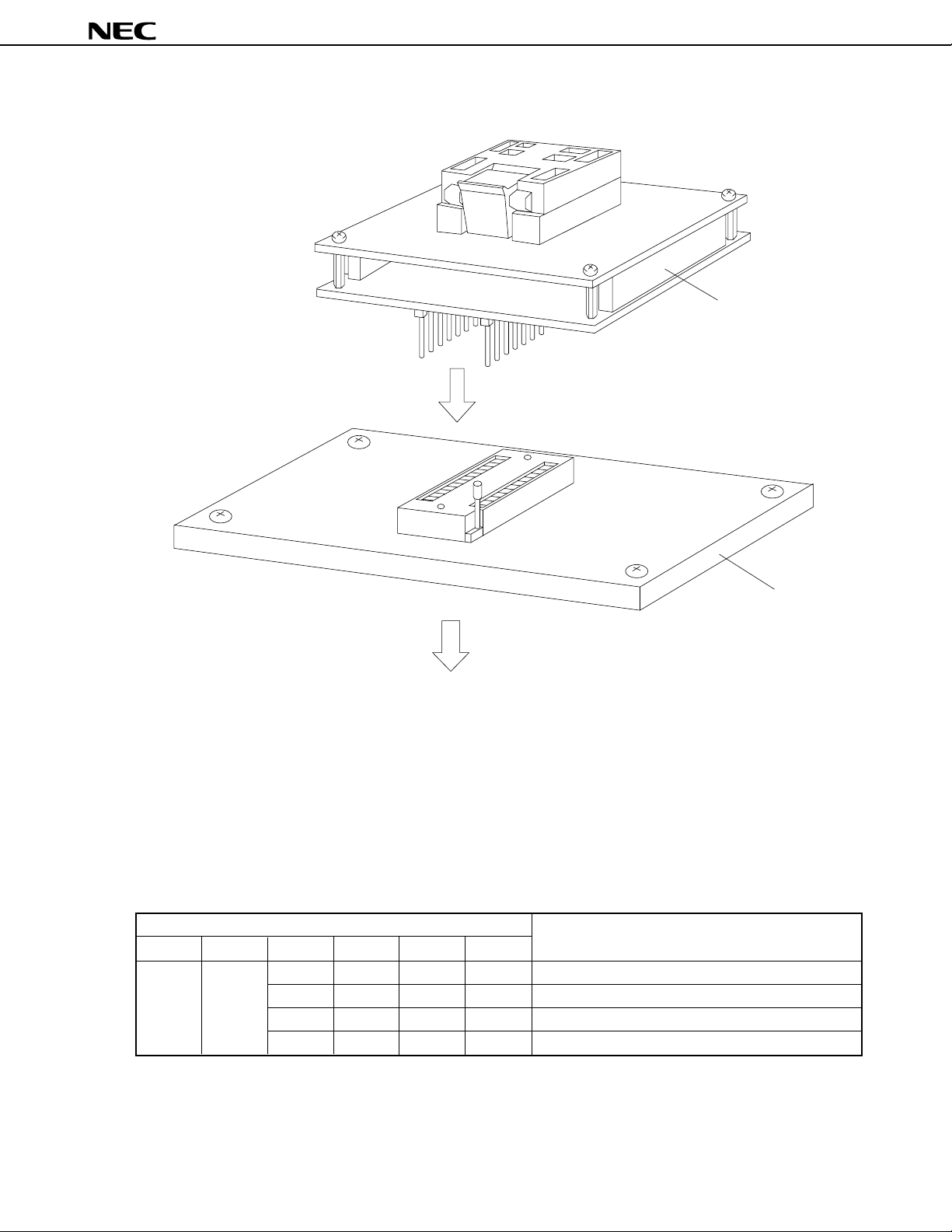
Figure 2-1. PA-17P709GC and PA-17KDZ
µ
PD17P709A
PA-17P709GC
PA-17KDZ
To PG-1500
2.1 Operation Modes for Program Memory Write, Read, and Verify
When +6 V is applied to the VDD pin and +12.5 V to the VPP pin, the µPD17P709A enters the program memory write,
read, and verify mode.
The following operation modes can be set by setting pins MD0 to MD3 as shown below.
Pins not listed in Table 2-2 should be connected to GND via a pull-down resistor (470 Ω) (refer to PIN
CONFIGURATION (2) PROM programming mode).
Table 2-2. Operation Mode Setting for Program Memory Write, Read, and Verify
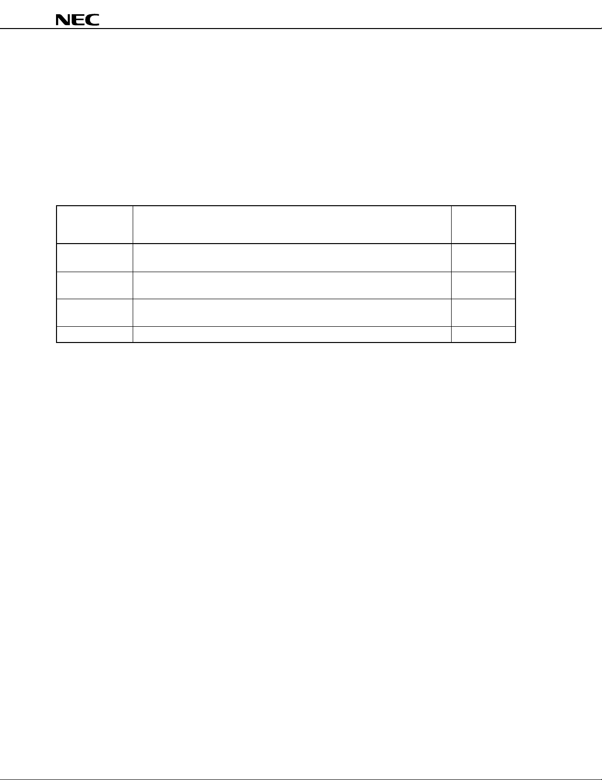
Operation Mode Setting Operation Mode
VPP VDD MD0 MD1 MD2 MD3
+12.5 V +6 V H L H L Program memory address 0-clear mode
L H H H Write mode
L L H H Write/verify mode
H × H H Program inhibit mode
Remark ×: L or H
Data Sheet U15723EJ1V0DS
23
2.2 Program Memory Write Procedure
Program memory can be written at high speed using the following procedure.
(1) Pull down unused pins to GND via a resistor. Set the CLK pin to low.
(2) Supply 5 V to the V
(3) Wait for 10
µ
(4) Set the mode setting pin to program memory address 0-clear mode.
(5) Supply +6 V to the V
(6) Set the program inhibit mode.
(7) Write data in the 1 ms write mode.
(8) Set the program inhibit mode.
(9) Set the verify mode. If the data is correct, go to step (10). If not, repeat steps (7) to (9).
(10) (X: Number of write operations from steps (7) to (9)) × 1 ms additional write.
(11) Set the program inhibit mode.
(12) Input four pulses to the CLK pin to increment the program memory address by one.
(13) Repeat steps (7) to (12) until the end address is reached.
(14) Set the program memory address 0-clear mode.
(15) Change the V
(16) Turn off the power.
DD pin. Set the VPP pin to low.
s and then supply 5 V to the VPP pin.
DD pin and +12.5 V to the VPP pin.
DD and VPP pins to 5 V.
µ
PD17P709A
The following figure shows steps (2) to (12).
X repetitions
Reset
Write
V
DD
+ 1
DD
V
PP
V
V
GND
V
V
GND
CLK
D0 to D7
MD0
MD1
MD2
DD
PP
DD
Hi - Z Hi - Z Hi - Z Hi - Z
Data input
Verify Additional write
Data output
Data input
Address
increment
24
MD3
Data Sheet U15723EJ1V0DS
µ
PD17P709A
2.3 Program Memory Read Procedure
(1) Pull down unused pins to GND via a resistor. Set the CLK pin to low.
(2) Supply 5 V to the V
(3) Wait for 10 µs and then supply 5 V to the VPP pin.
(4) Set the mode setting pin to program memory address 0-clear mode.
(5) Supply +6 V to the V
(6) Set the program inhibit mode.
(7) Set the verify mode. Addresses are incremented by one for each 4-pulse cycle input to the CLK pin.
(8) Set the program inhibit mode.
(9) Set the program memory address 0-clear mode.
(10) Change the V
(11) Turn off the power.
The following figure shows steps (2) to (9).
DD pin. Set the VPP pin to low.
DD pin and +12.5 V to the VPP pin.
DD and VPP pins to 5 V.
Reset
DD
V
PP
V
DD + 1
V
VDD
GND
VPP
VDD
GND
CLK
D0 to D7
MD0
MD1
MD2
MD3
Hi - Z Hi - Z
Data output
“L”
Data output
Data Sheet U15723EJ1V0DS
25

µ
PD17P709A
3. ELECTRICAL SPECIFICATIONS
Absolute Maximum Ratings (TA = 25°C)
Parameter Symbol Conditions Ratings Unit
Supply voltage VDD –0.3 to +6.0 V
PROM program voltage VPP –0.3 to +13.5 V
Input voltage VI Other than CE, INT0 to INT4, and RESET pins –0.3 to VDD + 0.3 V
CE, INT0 to INT4, and RESET pins –0.3 to VDD + 0.6 V
Output voltage VO Except P1B0 to P1B3 –0.3 to VDD + 0.3 V
Output current, high IOH Per pin –8.0 mA
Total of P2A0 to P2A2, P3A0 to P3A3, –15.0 mA
and P3B0 to P3B3
Total of P0A0 to P0A3, P0B0 to P0B3, P0C0 to P0C3, –25.0 mA
P1D0 to P1D3, P2B0 to P2B3, P2C0 to P2C3,
P2D0 to P2D2, P3C0 to P3C3, and P3D0 to P3D3
Output current, low IOL Per pin for P1B0 to P1B3 12.0 mA
Per pin for P1B0 to P1B3 8.0 mA
Total of P2A0 to P2A2, P3A0 to P3A3, 15.0 mA
and P3B0 to P3B3
Total of P0A0 to P0A3, P0B0 to P0B3, P0C0 to P0C3, 25.0 mA
P1D0 to P1D3, P2B0 to P2B3, P2C0 to P2C3,
P2D0 to P2D2, P3C0 to P3C3, and P3D0 to P3D3
Total of P1B0 to P1B3 pins 25.0 mA
Output voltage VBDS P1B0 to P1B3 14.0 V
Total power dissipation Pt 200 mW
Operating ambient TA –40 to +85 °C
temperature
Storage temperature Tstg –55 to +125 °C
Caution Product quality may suffer if the absolute maximum rating is exceeded even momentarily for any
parameter. That is, the absolute maximum ratings are rated values at which the product is on
the verge of suffering physical damage, and therefore the product must be used under conditions
that ensure that the absolute maximum ratings are not exceeded.
Recommended Operating Range (T
Parameter Symbol Conditions MIN. TYP. MAX. Unit
Supply voltage VDD1 When CPU and PLL are operating 4.5 5.0 5.5 V
VDD2 When CPU and PLL are stopped 3.5 5.0 5.5 V
A = –40 to +85°C)
Recommended Output Withstanding Voltage (TA = –40 to +85°C)
Parameter Symbol Conditions MIN. TYP. MAX. Unit
Output withstanding VBDS P1B0 to P1B3 12 V
voltage
26
Data Sheet U15723EJ1V0DS

µ
PD17P709A
DC Characteristics (TA = –40 to +85°C, VDD = 3.5 to 5.5 V)
Parameter Symbol Conditions MIN. TYP. MAX. Unit
Supply current IDD1 When CPU is operating and PLL is stopped with 1.5 3.0 mA
sine wave input to XIN pin.
(fIN = 4.5 MHz ±1%, VIN = VDD)
IDD2 When CPU and PLL are stopped with sine-wave 0.7 1.5 mA
input to XIN pin.
(fIN = 4.5 MHz ±1%, VIN = VDD)
With HALT instruction
Data retention voltage VDDR1 Crystal oscillation 3.5 5.5 V
VDDR2 Crystal oscillation Power failure detection by timer FF 2.2 5.5 V
VDDR3 stopped Data memory retained 2.0 5.5 V
Data retention current IDDR1 Crystal oscillation VDD = 5 V, TA = 25°C 2.0 4.0
IDDR2 stopped 2.0 30.0
Input voltage, high VIH1 P0A0, P0B1, P0C0 to P0C3, P1A0, P1A1, P1C0 to 0.7VDD VDD V
P1C3, P1D0 to P1D3, P2A2, P2B0 to P2B3,
P2C0 to P2C3, P2D0 to P2D2, P3A0 to P3A3,
P3B0 to P3B3, P3C0 to P3C3, P3D0 to P3D3
VIH2 P0A1 to P0A3, P0B0, P0B2, P0B3, P2A0, P2A1, CE, 0.8VDD VDD V
INT0 to INT4, RESET
VIH3 P0D0 to P0D3
Input voltage, low VIL1 P0A0, P0B1, P0C0 to P0C3, P1A0, P1A1, P1C0 to 0 0.3VDD V
P1C3, P1D0 to P1D3, P2A2, P2B0 to P2B3,
P2C0 to P2C3, P2D0 to P2D2, P3A0 to P3A3,
P3B0 to P3B3, P3C0 to P3C3, P3D0 to P3D3
VIL2 P0A1 to P0A3, P0B0, P0B2, P0B3, P2A0, P2A1, CE, 0 0.2VDD V
INT0 to INT4, RESET
VIL3 P0D0 to P0D3 0
Output current, high IOH1 P0A0 to P0A3, P0B0 to P0B3, P0C0 to P0C3, –1.0 mA
P1D0 to P1D3, P2A0 to P2A2, P2B0 to P2B3,
P2C0 to P2C3, P2D0 to P2D2, P3A0 to P3A3,
P3B0 to P3B3, P3C0 to P3C3, P3D0 to P3D3
VOH = VDD – 1 V
IOH2 EO0, EO1 VDD = 4.5 to 5.5 V, VOH = VDD – 1 V –3.0 mA
Output current, low IOL1 P0A0 to P0A3, P0B0 to P0B3, P0C0 to P0C3, 1.0 mA
P1D0 to P1D3, P2A0 to P2A2, P2B0 to P2B3,
P2C0 to P2C3, P2D0 to P2D2, P3A0 to PA3A,
P3B0 to P3B3, P3C0 to P3C3, P3D0 to P3D3
VOL = 1 V
IOL2 EO0, EO1 VDD = 4.5 to 5.5 V, VOL = 1 V 3.0 mA
IOL3 P1B0 to P1B3 VOL = 1 V 7.0 mA
Input current, high IIH P0D0 to P0D3 pulled down VIN = VDD 5.0 150
Output off leakage ILO1 P1B0 to P1B3 VIN = 12 V 1.0
current ILO2 EO0, EO1 VIN = VDD, VIN = 0 V ±1.0
Input leakage current, ILIH Input pin VIN = VDD 1.0
high
Input leakage current, low ILIL Input pin VIN = 0 V –1.0
0.55VDD
VDD V
0.15VDD
µ
A
µ
A
V
µ
A
µ
A
µ
A
µ
A
µ
A
Data Sheet U15723EJ1V0DS
27

µ
PD17P709A
AC Characteristics (TA = –40 to +85°C, VDD = 5 V ±10%)
Parameter Symbol Conditions MIN. TYP. MAX. Unit
Operating frequency f
SIO0 input frequency fIN7 External clock 1 MHz
IN1 VCOL pin, Sine-wave input VIN = 0.15Vp-p 0.8 3 MHz
MF mode Sine-wave input VIN = 0.1Vp-p 0.5 3 MHz
f
IN2 VCOL pin, HF mode, sine-wave input 10 40 MHz
VIN = 0.1Vp-p
fIN3 VCOH pin, VHF mode, sine-wave input 60 130 MHz
VIN = 0.1Vp-p
fIN4 AMIFC pin, sine-wave input 0.4 0.5 MHz
VIN = 0.15Vp-p
fIN5 FMIFC pin, FMIF count mode, sine-wave input 10 11 MHz
VIN = 0.20Vp-p
fIN6 FMIFC pin, AMIF count mode, sine-wave input 0.4 0.5 MHz
VIN = 0.15Vp-p
Note
Note
SIO1 input frequency f
IN8 External clock 0.7 MHz
Note The condition of sine-wave input VIN = 0.1Vp-p is the rated value when the µPD17P709A is operating alone.
Where influence of noise must be taken into consideration, operation under input amplitude conditions of
IN = 0.15Vp-p is recommended.
V
A/D Converter Characteristics (TA = –40 to +85°C, VDD = 5 V ±10%)
Parameter Symbol Conditions MIN. TYP. MAX. Unit
A/D conversion total error 8 bits ±3.0 LSB
A/D conversion total error 8 bits TA = 0 to 85°C ±2.5 LSB
Reference Characteristics (TA = +25°C, VDD = 5.0 V)
Parameter Symbol Conditions MIN. TYP. MAX. Unit
Supply current IDD3 When CPU and PLL are operating with sine-wave 6.0 12.0 mA
input to VCOH pin
(fIN = 130 MHz, VIN = 0.3Vp-p)
DC Programming Characteristics (TA = 25°C, VDD = 6.0 ±0.25 V, VPP = 12.5 ±0.5 V)
Parameter Symbol Conditions MIN. TYP. MAX. Unit
Input voltage, high VIH1 Pins other than CLK 0.7VDD VDD V
VIH2 CLK VDD – 0.5 VDD V
Input voltage, low VIL1 Pins other than CLK 0 0.2VDD V
VIL2 CLK 0 0.4 V
Input leakage current ILI VIN = VIL or VIH 10
Output voltage, high VOH IOH = –1 mA VDD – 1.0 V
Output voltage, low VOL IOL = 1 mA 1.0 V
VDD supply current IDD 30 mA
VPP supply current IPP MD0 = VIL, MD1 = VIH 30 mA
µ
A
Cautions 1. Ensure that VPP does not exceed +13.5 V including overshoot.
2. VDD must be applied before VPP, and cut after VPP.
28
Data Sheet U15723EJ1V0DS

µ
PD17P709A
AC Programming Characteristics (TA = 25°C, VDD = 6.0 ±0.25 V, VPP = 12.5 ±0.5 V)
Parameter Symbol Conditions MIN. TYP. MAX. Unit
Address setup time
MD1 setup time (to MD0↓)t
Data setup time (to MD0↓)tDS 2
Address hold time
Data hold time (from MD0↑)t
Delay time from MD0↑ to data output float
PP setup time (to MD3↑)tVPS 2
V
V
DD setup time (to MD3↑)tVDS 2
Initial program pulse width tPW 0.95 1.0 1.05 ms
Additional program pulse width t
MD0 setup time (to MD1↑)t
Delay time from MD0↓ to data output tDV MD0 = MD1 = VIL 1
MD1 hold time (from MD0↑)tM1H tM1H + tM1R ≥ 50 µs2
MD1 recovery time (from MD0↓)tM1R 2
Program counter reset time tPCR 10
CLK input high-/low-level widths tXH, tXL 0.125
CLK input frequency fX 4.19 MHz
Initial mode setting time tI 2
MD3 setup time (to MD1↑)tM3S 2
MD3 hold time (from MD1↓)tM3H 2
MD3 setup time (to MD0↓)tM3SR Program memory read 2
Delay time from address
Hold time from address
MD3 hold time (from MD0↑)tM3HR Program memory read 2
Delay time from MD3↓ to data output float
Reset setup time tRES 10
Note
(to MD0↓)tAS 2
M1S 2
Note
(from MD0↑)tAH 2
DH 2
tDF 0 130 ns
OPW 0.95 21.0 ms
M0S 2
Note
to data output
Note
to data output
tDAD Program memory read 2
tHAD Program memory read 0 130 ns
tDFR Program memory read 2
µ
s
µ
s
µ
s
µ
s
µ
s
µ
s
µ
s
µ
s
µ
s
µ
s
µ
s
µ
s
µ
s
µ
s
µ
s
µ
s
µ
s
µ
s
µ
s
µ
s
µ
s
Note The internal address signal is incremented by 1 on the 3rd fall of a four-clock input (CLK) cycle, and is not
connected to a pin.
Data Sheet U15723EJ1V0DS
29

Program Memory Write Timing
t
RES
t
t
M3S
VPS
t
VDS
Data input
DS
t
t
M1S
t
t
PW
t
M1H
PP
V
VDD + 1
V
DD
D0-D7
V
V
GND
V
GND
CLK
MD0
MD1
MD2
PP
DD
DD
tI
t
PCR
µ
PD17P709A
t
XH
t
Data output
DH
t
M1R
t
DV
t
DF
t
M0S
Data input Data input
t
DS
t
OPW
XL
t
DH
t
AH
t
AS
t
M3H
MD3
Remark The dashed line indicates high-impedance.
Program Memory Read Timing
RES
t
V
PP
PP
V
V
DD
GND
V
DD
V
+ 1
DD
DD
V
GND
CLK
D0-D7
I
t
MD0
t
VPS
t
VDS
t
XH
t
XL
Hi-Z Hi-Z
Data output Data output
t
DV
t
t
DAD
HAD
t
M3HR
t
DFR
30
MD1
MD2
MD3
L
t
PCR
t
M3SR
Data Sheet U15723EJ1V0DS

4. PACKAGE DRAWING
80-PIN PLASTIC QFP (14x14)
µ
PD17P709A
A
B
61
80
60
1
41
20
40
21
F
G
H
M
I
P
SN
NOTE
Each lead centerline is located within 0.13 mm of
its true position (T.P.) at maximum material condition.
L
detail of lead end
S
C D
Q
R
J
K
S
M
ITEM MILLIMETERS
A
17.2±0.4
B
14.0±0.2
C 14.0±0.2
D
17.2±0.4
F 0.825
G
0.825
H 0.30±0.10
0.13
I
J
0.65 (T.P.)
K
1.6±0.2
L
0.8±0.2
M 0.15
N
P
Q
R
S
+0.10
−0.05
0.10
2.7±0.1
0.1±0.1
5°±5°
3.0 MAX.
S80GC-65-3B9-6
Data Sheet U15723EJ1V0DS
31
µ
PD17P709A
5. RECOMMENDED SOLDERING CONDITIONS
The µPD17P709A should be soldered and mounted under the following recommended conditions.
For details of the recommended soldering conditions, refer to the document Semiconductor Device Mounting
Technology Manual (C10535E).
For soldering methods and conditions other than those recommended below, contact an NEC sales representative.
Table 5-1. Surface Mounting Type Soldering Conditions
µ
PD17P709AGC-3B9: 80-pin plastic QFP (14 × 14)
Soldering Method Soldering Conditions Recommended
Condition
Symbol
Infrared reflow Package peak temperature: 235°C, Time: 30 seconds MAX. (at 210°C or higher.), IR35-00-3
Count: Three times or less
VPS Package peak temperature: 215°C, Time: 40 seconds MAX. (at 200°C or higher.), VP15-00-3
Count: Three times or less
Wave soldering Solder bath temperature: 260°C MAX., Time: 10 seconds MAX., Count: Once, WS60-00-1
Preheating temperature: 120°C MAX. (package surface temperature)
Partial heating Pin temperature: 300°C MAX., Time: 3 seconds MAX. (per pin row) —
Caution Do not use different soldering methods together (except for partial heating).
32
Data Sheet U15723EJ1V0DS
µ
APPENDIX DEVELOPMENT TOOLS
The following development tools are available for development of programs for the µPD17P709A.
Hardware
Name Outline
In-circuit emulator
(IE-17K-ET
SE board
(SE-17709)
Emulation probe
(EP-17K80GC)
Conversion socket
(EV-9200GC-80
PROM programmer
(PG-1500)
Programmer adapter
(PA-17P709GC)
Note 1
)
Note 2
IE-17K-ET is an in-circuit emulator that can be used with any model in the 17K Series.
IE-17K-ET is connected to a host machine, which is PC-9800 series or IBM PC/ATTM, with RS-232C.
By using these in-circuit emulators with a system evaluation board (SE board) corresponding to each
model, these emulators operate as emulators specific to a model. When man-machine interface
software
SE-17709 is an SE board for the µPD17709A Subseries. This board can be used alone to evaluate
a system, or in combination with an in-circuit emulator for debugging.
EP-17K80GC is an emulation probe for the µPD17P709AGC. By using this probe with EV-9200GC-
80
EV-9200GC-80 is a conversion socket for 80-pin plastic QFP (14 × 14). It is used to connect the EP-
)
17K80GC and target system.
PG-1500 is a PROM programmer supporting µPD17P709A. It can program the µPD17P709A when
connected with the PG-1500 adapter PA-17KDZ and programmer adapter PA-17P709GC.
PA-17P709GC is an adapter to program the µPD17P709A. It is used with PG-1500.
SIMPLEHOST
Note 2
, the SE board and target system are connected.
TM
is used, a more sophisticated debugging environment can be created.
PD17P709A
Notes 1. External power supply type
2. One EV-9200GC-80 is supplied with the EP-17K80GC. Five EV-9200GC-80 are also available as a set.
Remark Third-party PROM programmers AF-9703, AF-9704, AF-9705, and AF-9706 are available from Ando
Electric Co., Ltd. Use these programmers with programmer adapter PA-17P709GC. For details, consult
Ando Electric Co., Ltd. (TEL: +8-44-549-7300).
Software
Name Outline Host Machine OS Media Parts Number
17K Series PC-9800 series
assembler
(RA17K) IBM PC/AT
Device file PC-9800 series
(AS17704)
Support PC-9800 series
software
(
SIMPLEHOST
RA17K is an assembler that can be
commonly used with 17K Series.
To develop programs for the
µ
PD17P709A, this RA17K and a
device file (AS17704) are used in
combination.
AS17704 is a device file for the
µ
PD17P709A.
It is used with the assembler common
to the 17K Series (RA17K).
SIMPLEHOST
interface software that runs on
Windows when a program is
) IBM PC/AT
developed by using an in-circuit
emulator and personal computer.
is man-machine
compatibles English Windows
IBM PC/AT
compatibles English Windows
compatibles English Windows
Japanese WindowsTM3.5” 2HDµSAA13RA17K
Japanese Windows
Japanese Windows
Japanese Windows
Japanese Windows
Japanese Windows
3.5” 2HCµSAB13RA17K
µ
SBB13RA17K
3.5” 2HDµSAA13AS17704
3.5” 2HCµSAB13AS17704
µ
SBB13AS17704
3.5” 2HDµSAA13ID17K
3.5” 2HCµSAB13ID17K
µ
SBB13ID17K
Data Sheet U15723EJ1V0DS
33
NOTES FOR CMOS DEVICES
1 PRECAUTION AGAINST ESD FOR SEMICONDUCTORS
Note:
Strong electric field, when exposed to a MOS device, can cause destruction of the gate oxide and
ultimately degrade the device operation. Steps must be taken to stop generation of static electricity
as much as possible, and quickly dissipate it once, when it has occurred. Environmental control
must be adequate. When it is dry, humidifier should be used. It is recommended to avoid using
insulators that easily build static electricity. Semiconductor devices must be stored and transported
in an anti-static container, static shielding bag or conductive material. All test and measurement
tools including work bench and floor should be grounded. The operator should be grounded using
wrist strap. Semiconductor devices must not be touched with bare hands. Similar precautions need
to be taken for PW boards with semiconductor devices on it.
2 HANDLING OF UNUSED INPUT PINS FOR CMOS
Note:
No connection for CMOS device inputs can be cause of malfunction. If no connection is provided
to the input pins, it is possible that an internal input level may be generated due to noise, etc., hence
causing malfunction. CMOS devices behave differently than Bipolar or NMOS devices. Input levels
of CMOS devices must be fixed high or low by using a pull-up or pull-down circuitry. Each unused
pin should be connected to V
being an output pin. All handling related to the unused pins must be judged device by device and
related specifications governing the devices.
DD or GND with a resistor, if it is considered to have a possibility of
µ
PD17P709A
3 STATUS BEFORE INITIALIZATION OF MOS DEVICES
Note:
Power-on does not necessarily define initial status of MOS device. Production process of MOS
does not define the initial operation status of the device. Immediately after the power source is
turned ON, the devices with reset function have not yet been initialized. Hence, power-on does
not guarantee out-pin levels, I/O settings or contents of registers. Device is not initialized until the
reset signal is received. Reset operation must be executed immediately after power-on for devices
having reset function.
34
Data Sheet U15723EJ1V0DS

µ
PD17P709A
Regional Information
Some information contained in this document may vary from country to country. Before using any NEC
product in your application, pIease contact the NEC office in your country to obtain a list of authorized
representatives and distributors. They will verify:
•
Device availability
•
Ordering information
•
Product release schedule
•
Availability of related technical literature
•
Development environment specifications (for example, specifications for third-party tools and
components, host computers, power plugs, AC supply voltages, and so forth)
•
Network requirements
In addition, trademarks, registered trademarks, export restrictions, and other legal issues may also vary
from country to country.
NEC Electronics Inc. (U.S.)
Santa Clara, California
Tel: 408-588-6000
800-366-9782
Fax: 408-588-6130
800-729-9288
NEC Electronics (Germany) GmbH
Duesseldorf, Germany
Tel: 0211-65 03 02
Fax: 0211-65 03 490
NEC Electronics (UK) Ltd.
Milton Keynes, UK
Tel: 01908-691-133
Fax: 01908-670-290
NEC Electronics Italiana s.r.l.
Milano, Italy
Tel: 02-66 75 41
Fax: 02-66 75 42 99
NEC Electronics (Germany) GmbH
Benelux Office
Eindhoven, The Netherlands
Tel: 040-2445845
Fax: 040-2444580
NEC Electronics (France) S.A.
Velizy-Villacoublay, France
Tel: 01-3067-5800
Fax: 01-3067-5899
NEC Electronics (France) S.A.
Madrid Office
Madrid, Spain
Tel: 091-504-2787
Fax: 091-504-2860
NEC Electronics (Germany) GmbH
Scandinavia Office
Taeby, Sweden
Tel: 08-63 80 820
Fax: 08-63 80 388
NEC Electronics Hong Kong Ltd.
Hong Kong
Tel: 2886-9318
Fax: 2886-9022/9044
NEC Electronics Hong Kong Ltd.
Seoul Branch
Seoul, Korea
Tel: 02-528-0303
Fax: 02-528-4411
NEC Electronics Singapore Pte. Ltd.
Novena Square, Singapore
Tel: 253-8311
Fax: 250-3583
NEC Electronics Taiwan Ltd.
Taipei, Taiwan
Tel: 02-2719-2377
Fax: 02-2719-5951
NEC do Brasil S.A.
Electron Devices Division
Guarulhos-SP, Brasil
Tel: 11-6462-6810
Fax: 11-6462-6829
Data Sheet U15723EJ1V0DS
J01.2
35

µ
PD17P709A
Purchase of NEC I2C components conveys a license under the Philips I2C Patent Rights to use these
2
components in an I
by Philips.
C system, provided that the system conforms to the I2C Standard Specification as defined
SIMPLEHOST
Windows is either a registered trademark or trademark of Microsoft Corporation in the United States and/
or other countries.
PC/AT is a trademark of International Business Machines Corporation.
The export of this product from Japan is regulated by the Japanese government. To export this product may be prohibited
without governmental license, the need for which must be judged by the customer. The export or re-export of this product
from a country other than Japan may also be prohibited without a license from that country. Please call an NEC sales
representative.
•
The information in this document is current as of September, 2001. The information is subject to
change without notice. For actual design-in, refer to the latest publications of NEC's data sheets or
data books, etc., for the most up-to-date specifications of NEC semiconductor products. Not all
products and/or types are available in every country. Please check with an NEC sales representative
for availability and additional information.
•
No part of this document may be copied or reproduced in any form or by any means without prior
written consent of NEC. NEC assumes no responsibility for any errors that may appear in this document.
•
NEC does not assume any liability for infringement of patents, copyrights or other intellectual property rights of
third parties by or arising from the use of NEC semiconductor products listed in this document or any other
liability arising from the use of such products. No license, express, implied or otherwise, is granted under any
patents, copyrights or other intellectual property rights of NEC or others.
•
Descriptions of circuits, software and other related information in this document are provided for illustrative
purposes in semiconductor product operation and application examples. The incorporation of these
circuits, software and information in the design of customer's equipment shall be done under the full
responsibility of customer. NEC assumes no responsibility for any losses incurred by customers or third
parties arising from the use of these circuits, software and information.
•
While NEC endeavours to enhance the quality, reliability and safety of NEC semiconductor products, customers
agree and acknowledge that the possibility of defects thereof cannot be eliminated entirely. To minimize
risks of damage to property or injury (including death) to persons arising from defects in NEC
semiconductor products, customers must incorporate sufficient safety measures in their design, such as
redundancy, fire-containment, and anti-failure features.
•
NEC semiconductor products are classified into the following three quality grades:
"Standard", "Special" and "Specific". The "Specific" quality grade applies only to semiconductor products
developed based on a customer-designated "quality assurance program" for a specific application. The
recommended applications of a semiconductor product depend on its quality grade, as indicated below.
Customers must check the quality grade of each semiconductor product before using it in a particular
application.
"Standard": Computers, office equipment, communications equipment, test and measurement equipment, audio
"Special": Transportation equipment (automobiles, trains, ships, etc.), traffic control systems, anti-disaster
"Specific": Aircraft, aerospace equipment, submersible repeaters, nuclear reactor control systems, life
The quality grade of NEC semiconductor products is "Standard" unless otherwise expressly specified in NEC's
data sheets or data books, etc. If customers wish to use NEC semiconductor products in applications not
intended by NEC, they must contact an NEC sales representative in advance to determine NEC's willingness
to support a given application.
(Note)
(1) "NEC" as used in this statement means NEC Corporation and also includes its majority-owned subsidiaries.
(2) "NEC semiconductor products" means any semiconductor product developed or manufactured by or for
NEC (as defined above).
2
is a trademark of NEC Corporation.
and visual equipment, home electronic appliances, machine tools, personal electronic equipment
and industrial robots
systems, anti-crime systems, safety equipment and medical equipment (not specifically designed
for life support)
support systems and medical equipment for life support, etc.
M8E 00. 4
 Loading...