

DATA SHEET
MOS INTEGRATED CIRCUIT
µ
PD17P236
4-BIT SINGLE-CHIP MICROCONTROLLER
FOR SMALL GENERAL-PURPOSE INFRARED
REMOTE CONTROLLER
The µPD17P236 is a model of the µPD17236 with a one-time PROM instead of an internal mask ROM.
Since the user can write programs to the µPD17P236, it is ideal for experimental production or small-scale
µ
production of the
When reading this document, also read the documents related to the µPD17230, 17231, 17232, 17233, 17234,
17235, and 17236.
Detailed functions are described in the following user's manual. Read this manual when designing your system.
PD17230, 17231, 17232, 17233, 17234, 17235, or 17236 systems.
µ
PD172×× Series User's Manual: U12795E
FEATURES
• Pin compatible with µPD17230, 17231, 17232, 17233, 17234, 17235, and 17236 (except PROM programming
function)
• Carrier generator circuit for infrared remote controller (REM output)
• 17K architecture: General-purpose register method
• Program memory (one-time PROM): 32 Kbytes (16,384 × 16)
• Data memory (RAM): 223 × 4 bits
• Low-voltage detection circuit
• Input/output of P1A
Input/output of P1A0 pin Output Input Output Input
Clock (RfX) selection for carrier generation RfX = fX/2 RfX = fX
• Supply voltage: VDD = 2.2 to 3.6 V (fX = 4 MHz: high-speed mode, 4 µs)
APPLICATIONS
Preset remote controllers, toys, and portable systems
0 pin, clock selection for carrier generation
µ
PD17P236M1µPD17P236M2µPD17P236M3µPD17P236M4
VDD = 3.0 to 3.6 V (fX = 8 MHz: high-speed mode, 2 µs)
The information in this document is subject to change without notice. Before using this document, please
confirm that this is the latest version.
Not all devices/types available in every country. Please check with local NEC representative for
availability and additional information.
Document No. U14776EJ1V0DS00 (1st edition)
Date Published June 2000 J CP(K)
Printed in Japan
©
2000
ORDERING INFORMATION
Part Number Package
µ
PD17P236M1GT 28-pin plastic SOP (9.53 mm (375))
µ
PD17P236M1MC-5A4 30-pin plastic SSOP (7.62 mm (300))
µ
PD17P236M2GT 28-pin plastic SOP (9.53 mm (375))
µ
PD17P236M2MC-5A4 30-pin plastic SSOP (7.62 mm (300))
µ
PD17P236M3GT 28-pin plastic SOP (9.53 mm (375))
µ
PD17P236M3MC-5A4 30-pin plastic SSOP (7.62 mm (300))
µ
PD17P236M4GT 28-pin plastic SOP (9.53 mm (375))
µ
PD17P236M4MC-5A4 30-pin plastic SSOP (7.62 mm (300))
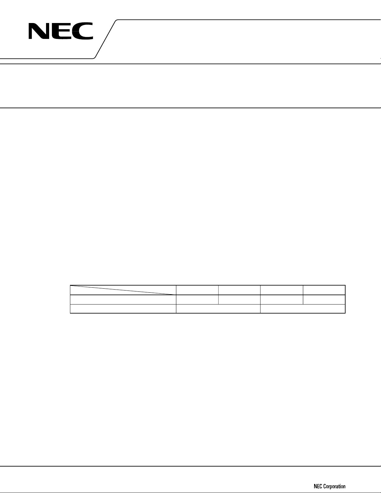
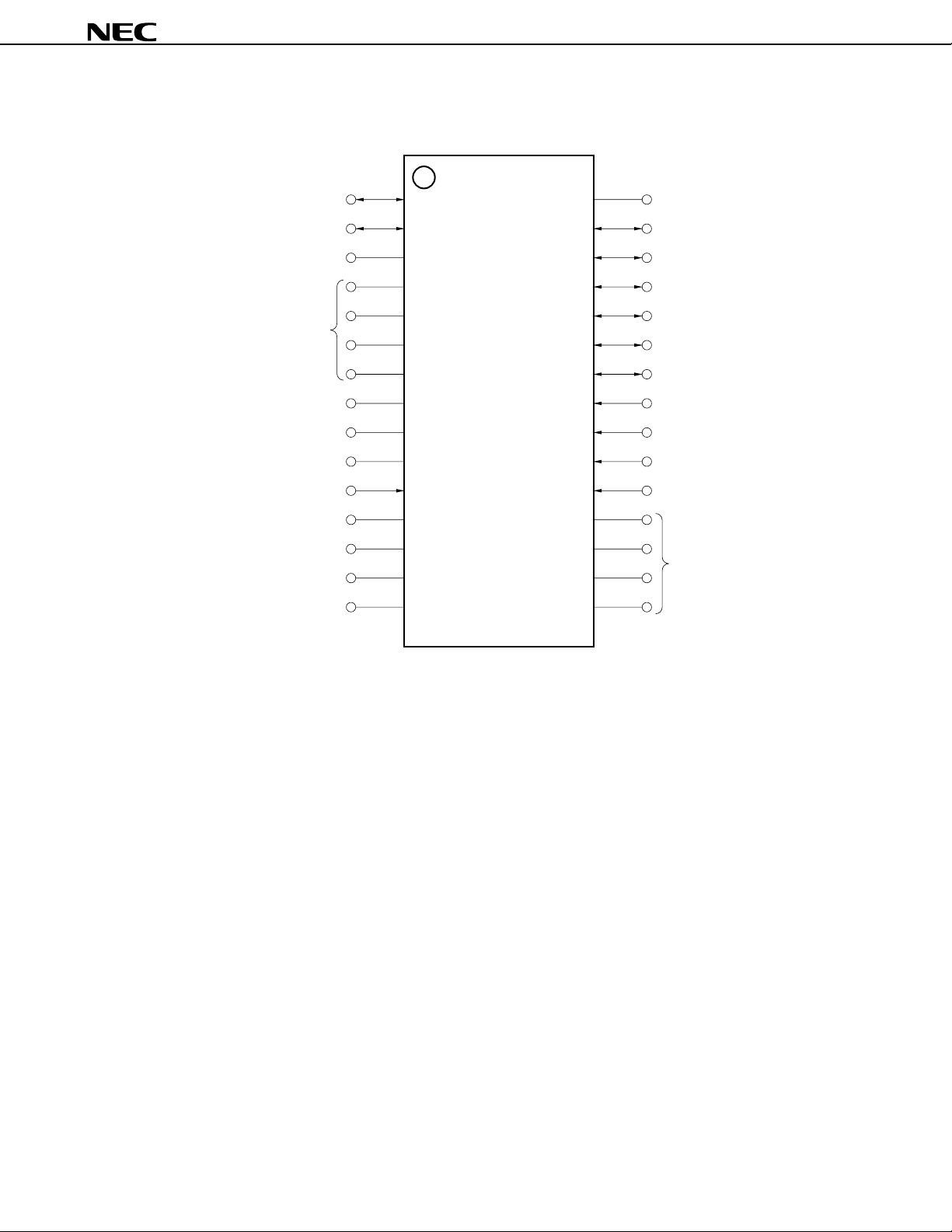
PIN CONFIGURATION (TOP VIEW)
(1) Normal operation mode
• 28-pin plastic SOP (9.53 mm (375))
µ
PD17P236M1GT, 17P236M2GT, 17P236M3GT, 17P236M4GT
µ
PD17P236
P0D
P0D
INT
P0E
P0E
P0E
P0E
REM
V
X
OUT
X
GND
RESET
P1A
2
3
1
2
3
0
1
2
3
4
5
6
7
8
DD
9
10
IN
11
12
13
0
14
28
27
26
25
24
23
22
21
20
19
18
17
16
15
P0D
P0D
P0C
P0C
P0C
P0C
P0B
P0B
P0B
P0B
P0A
P0A
P0A
P0A
1
0
3
2
1
0
3
2
1
0
3
2
1
0
2
Data Sheet U14776EJ1V0DS00
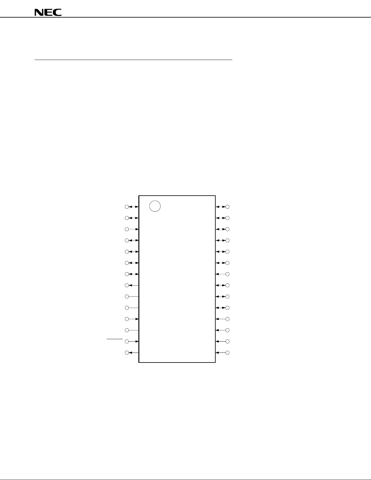
• 30-pin plastic SSOP (7.62 mm (300))
µ
PD17P236M1MC-5A4, 17P236M2MC-5A4, 17P236M3MC-5A4, 17P236M4MC-5A4
µ
PD17P236
P0D
P0D
INT
P0E
P0E
P0E
P0E
REM
V
X
OUT
X
GND
RESET
P1A
IC1
2
3
1
2
3
0
1
2
3
4
5
6
7
8
DD
9
10
IN
11
12
13
0
14
15
30
29
28
27
26
25
24
23
22
21
20
19
18
17
16
IC2
P0D
P0D
P0C
P0C
P0C
P0C
P0B
P0B
P0B
P0B
P0A
P0A
P0A
P0A
1
0
3
2
1
0
3
2
1
0
3
2
1
0
GND : Ground
IC1, IC2 : Internally connected
Note 1
INT : External interrupt request signal input
P0A0-P0A3 : Input port (CMOS input)
0-P0B3 : Input/output port (CMOS input/N-ch open-drain output)
P0B
P0C0-P0C3 : Input/output port (CMOS input/N-ch open-drain output)
P0D0-P0D3 : Input/output port (CMOS input/N-ch open-drain output)
0-P0E3 : Input/output port (CMOS push-pull output)
P0E
P1A0 : Input port (CMOS input) or output port (N-ch open-drain output)
REM : Remote controller output (CMOS push-pull output)
RESET : Reset input
DD : Power supply
V
XIN, XOUT : Resonator connection
Notes 1. This pin cannot be used. Leave open.
2. Input port or output port is selected depending on the product (see 2. PIN
FUNCTIONS).
Note 2
Data Sheet U14776EJ1V0DS00
3
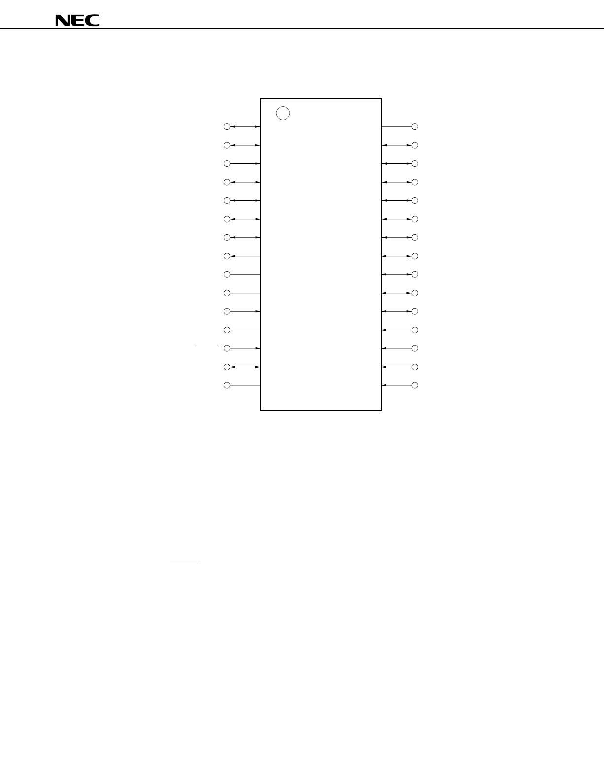
(2) PROM programming mode
• 28-pin plastic SOP (9.53 mm (375))
µ
PD17P236M1GT, 17P236M2GT, 17P236M3GT, 17P236M4GT
D
2
D
3
V
PP
(L)
µ
PD17P236
D
D
D
D
D
D
MD
1
0
7
6
5
4
3
1
2
3
4
5
6
7
28
27
26
25
24
23
22
(Open)
V
(Open)
CLK
GND
(L)
(Open)
MD
MD
MD
2
1
0
8
DD
9
10
11
12
21
20
19
18
17
(L)
13
14
16
15
4
Data Sheet U14776EJ1V0DS00
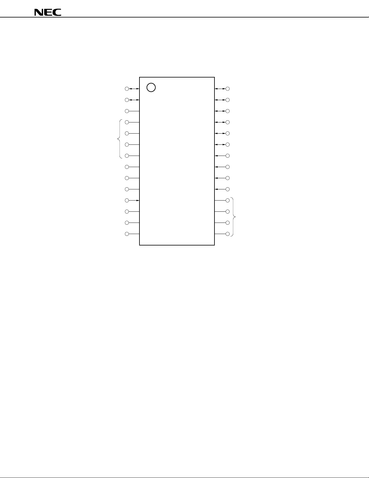
• 30-pin plastic SSOP (7.62 mm (300))
µ
PD17P236M1MC-5A4, 17P236M2MC-5A4, 17P236M3MC-5A4, 17P236M4MC-5A4
µ
PD17P236
D
D3
VPP
(L)
(Open)
V
(Open)
CLK
GND
(L)
(Open)
(Open)
2
DD
1
2
3
4
5
6
7
8
9
10
11
12
13
14
15
30
29
28
27
26
25
24
23
22
21
20
19
18
17
16
(Open)
D
1
D0
D7
D6
D5
D4
MD3
MD2
MD1
MD0
(L)
Caution Contents in parentheses indicate how to handle unused pins in PROM programming mode.
L : Connect to GND via a resistor (470
Ω) separately.
Open : Leave unconnected.
CLK : Clock input for PROM
0-D7 : Data input/output for PROM
D
GND : Ground
0-MD3 : Mode select input for PROM
MD
VDD : Power supply
VPP : Power supply for PROM writing
Data Sheet U14776EJ1V0DS00
5
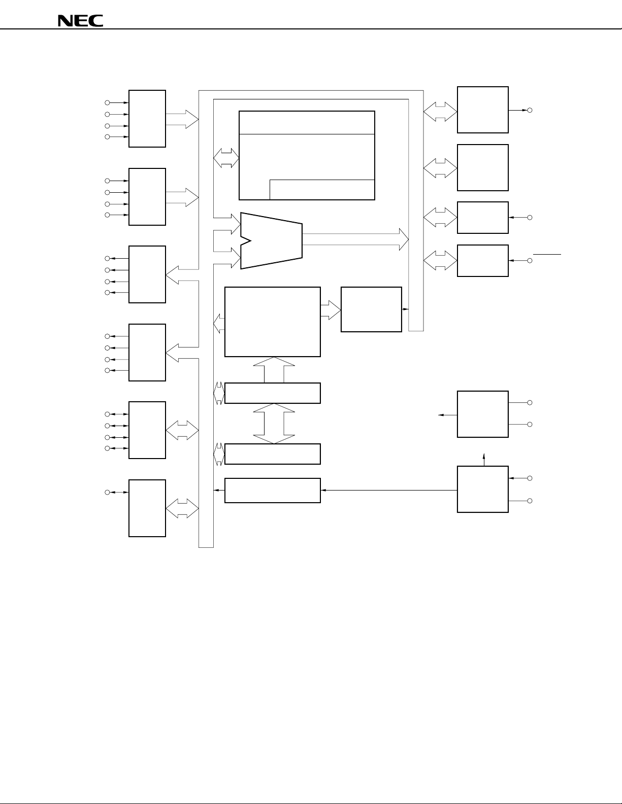
BLOCK DIAGRAM
µ
PD17P236
P0A
P0A
P0A
P0A
P0B0 (MD0)
1
(MD1)
P0B
2
(MD2)
P0B
3
(MD3)
P0B
P0C0 (D4)
1
(D5)
P0C
2
(D6)
P0C
3
(D7)
P0C
P0D0 (D0)
1
(D1)
P0D
2
(D2)
P0D
3
(D3)
P0D
0
1
2
3
P0A
RF
Remote
Control
Divider
REM
RAM
223 × 4 bits
8-bit
timer
P0B
SYSTEM REG.
Interrupt
Controller
INT (V
PP
)
ALU
Reset
Controller
RESET
P0C
Instruction
One Time PROM
Decoder
16,384 × 16 bits
P0D
Program Counter
Power
P0E
P1A
P0E
P0E
P0E
Note
0
0
1
2
3
P0E
Stack (5 levels)
Basic Interval/
Watchdog Timer
Supply
Circuit
CPU Clock
P1A
Note Input port or output port is selected depending on the product (see 2. PIN FUNCTIONS).
Remark ( ): During PROM programming mode
OSC
DD
V
GND
IN
X
OUT
X
(CLK)
6
Data Sheet U14776EJ1V0DS00

µ
PD17P236
CONTENTS
1. DIFFERENCES BETWEEN µPD17236 AND µPD17P236 ........................................................... 8
2. PIN FUNCTIONS ........................................................................................................................... 9
2.1 Normal Operation Mode .................................................................................................................... 9
2.2 PROM Programming Mode ............................................................................................................... 10
2.3 Input/Output Circuits ......................................................................................................................... 11
2.4 Processing of Unused Pins .............................................................................................................. 12
2.5 Notes on Using the RESET and INT Pins ........................................................................................12
3. WRITING AND VERIFYING ONE-TIME PROM (PROGRAM MEMORY) .................................... 13
3.1 Operating Mode When Writing/Verifying Program Memory .......................................................... 13
3.2 Program Memory Writing Procedure ............................................................................................... 14
3.3 Program Memory Reading Procedure .............................................................................................15
4. ELECTRICAL SPECIFICATIONS ................................................................................................. 16
5. PACKAGE DRAWING .................................................................................................................. 23
6. RECOMMENDED SOLDERING CONDITIONS ............................................................................ 25
APPENDIX. DEVELOPMENT TOOLS................................................................................................ 27
Data Sheet U14776EJ1V0DS00
7
µ
PD17P236
1. DIFFERENCES BETWEEN µPD17236 AND µPD17P236
µ
PD17P236 is equipped with PROM to which data can be written by the user instead of the internal mask ROM
(program memory) of the µPD17236.
µ
Table 1-1 shows the differences between the
The CPU functions and internal hardware of the µPD17P236, 17230, 17231, 17232, 17233, 17234, 17235, and
17236 are identical. Therefore, the µPD17P236 can be used to evaluate the program developed for the µPD17230,
17231, 17232, 17233, 17234, 17235, and 17236 system. Note, however, that some of the electrical specifications
such as supply current and low-voltage detection voltage of the
µ
PD17230, 17231, 17232, 17233, 17234, 17235, and 17236.
Table 1-1. Differences among
PD17236 and µPD17P236.
µ
PD17P236 are different from those of the
µ
PD17236 and µPD17P236
Product Name
Item 17P236M3, 17P236M4
Program memory One-time PROM Mask ROM
32 Kbytes (16,384 × 16)
(0000H-3FFFH)
Data memory 223 × 4 bits
Input/output of P1A0 pin • Input (µPD17P236M2, 17P236M4) Any (mask option)
• Output (µPD17P236M1, 17P236M3)
Clock (RfX) selection for carrier • RfX = fX/2 (µPD17P236M1, 17P236M2) Any (mask option)
generation • RfX = fX (µPD17P236M3, 17P236M4)
Low-voltage detection circuit
Instruction execution time • 2 µs (VDD = 3.0 to 3.6 V) • 2 µs (VDD = 2.2 to 3.6 V)
Supply voltage VDD = 2.2 to 3.6 V VDD = 2.0 to 3.6 V
Package • 28-pin plastic SOP (9.53 mm (375))
Note
Provided Any (mask option)
• 4 µs (VDD = 2.2 to 3.6 V) • 4 µs (VDD = 2.0 to 3.6 V)
• 30-pin plastic SSOP (7.62 mm (300))
µ
PD17P236
µ
PD17P236M1, 17P236M2,
µ
PD17236
Note Although the circuit configuration is identical, its electrical characteristics differ depending on the product.
8
Data Sheet U14776EJ1V0DS00
2. PIN FUNCTIONS
2.1 Normal Operation Mode (1/2)
µ
PD17P236
Pin No. Symbol Function
27 (28) P0D0 These pins constitute a 4-bit I/O port which can be set in the input N-ch Low-level
28 (29) P0D1 or output mode in 4-bit units (group I/O). open-drain output
1 (1) P0D2 In the input mode, these pins serve as CMOS input pins with a
2 (2) P0D3 pull-up resistor, and can be used as key return input lines of a key
matrix. The standby status must be released when at least one of
the input lines goes low. In the output mode, these pins are used
as N-ch open-drain output pins and can be used as the output
lines of a key matrix.
3 (3) INT External interrupt request signal. This signal releases the standby – Input
status if an external interrupt request signal is input to it when the
INT pin interrupt enable flag (IP) is set.
4 (4) P0E0 These pins constitute a 4-bit I/O port that can be set in the input or CMOS Input
5 (5) P0E1 output mode in 1-bit units. push-pull
6 (6) P0E2 In the output mode, this port functions as a high current CMOS
7 (7) P0E3 output port. In the input mode, function as CMOS input and can be
specified to connect pull-up resistor by program.
8 (8) REM Outputs transfer signal for infrared remote controller. CMOS Low-level
Active-high output. push-pull output
9 (9) VDD Power supply – –
10 (10) XOUT Connects ceramic resonator for system clock oscillation – (Oscillation
11 (11) XIN stops)
12 (12) GND Ground – –
13 (13) RESET Turns ON pull down resistor if POC or watchdog timer overflows – Input
and if the stack pointer overflows or underflows, and resets the
system. Usually, the pull-down resistor is ON.
14 (14) P1A0
15 (16) P0A0 These pins are CMOS input pins with a 4-bit pull-up resistor. – Input
16 (17) P0A1 They can be used as the key return input lines of a key matrix.
17 (18) P0A2 If any one of these pins goes low, the standby status is released.
18 (19) P0A3
19 (20) P0B0 These pins constitute a 4-bit I/O port that can be set in the input or N-ch Input
20 (21) P0B1 output mode in 1-bit units. open-drain
21 (22) P0B2 In the input mode, these pins are CMOS input pins with a pull-up
22 (23) P0B3 resistor, and can be used as the key return input lines of a key
µ
PD17P136M1, This pin is 1-bit output port (N-ch open-drain N-ch High-
µ
PD17P136M3 output) and can be used as the output lines of open-drain impedance
a key matrix. output
µ
PD17P136M2, This pin is 1-bit input port (CMOS input). – Input
µ
PD17P136M4 However, it cannot release the STOP mode.
matrix. The standby status is released when at least one of these
pins goes low.
In the output mode, they serve as N-ch open-drain output pins and
can be used as the output lines of a key matrix.
Output Format
At Reset
Remark The number in parenthesis in the Pin No. column indicates the pin numbers of the 30-pin plastic SSOP.
Data Sheet U14776EJ1V0DS00
9
2.1 Normal Operation Mode (2/2)
µ
PD17P236
Pin No. Symbol Function
23 (24) P0C0 These pins constitute a 4-bit I/O port that can be set in the input or N-ch Low-level
24 (25) P0C1 output mode in 4-bit units (group I/O). open-drain output
25 (26) P0C2 In the input mode, these pins are CMOS input pins with a pull-up
26 (27) P0C3 resistor, and can be used as the key return input lines of a key
matrix. The standby status is released when at least one of these
pins goes low.
In the output mode, they serve as N-ch open-drain output pins and
can be used as the output lines of a key matrix.
(15) IC1 These pins cannot be used. – –
(30) IC2 Leave open.
Output Format
At Reset
Remark The number in parenthesis in the Pin No. column indicates the pin numbers of the 30-pin plastic SSOP.
2.2 PROM Programming Mode
Pin No. Symbol Function
3VPP Power supply for PROM programming. – –
Apply +12.5 V to this pin as the program voltage when writing/
verifying program memory.
9VDD Power supply. Apply +6 V to this pin when writing/verifying – –
program memory.
11 CLK Inputs clock for PROM programming. – –
12 GND Ground. – –
19 (20) MD0 Input pins used to select operation mode when PROM is – Input
programmed.
22 (23) MD3
23 (24) D4 Input/output 8-bit data for PROM programming CMOS Input
push-pull
26 (27) D7
27 (28) D0
28 (29) D1
1D2
2D3
Output Format
At Reset
Remarks 1. The other pins are not used in the PROM programming mode. How to handle the other opins are
described in PIN CONFIGURATION (2) PROM programming mode.
2. The number in parenthesis in the Pin No. column indicates the pin numbers of the 30-pin plastic
SSOP.
10
Data Sheet U14776EJ1V0DS00

2.3 Input/Output Circuits
The equivalent input/output circuit for each µPD17P236 pin is shown below.
µ
PD17P236
(1) P0A
Input buffer
(2) P0B, P0C, P0D
Data
Output
disable
Output
latch
Selector
VDD
N-ch
(4) P1A
• Input mode (
µ
PD17P236M2, 17P236M4)
Input buffer
• Output mode (µPD17P236M1, 17P236M3)
V
DD
data N-ch
P-ch
Output
latch
(5) RESET
V
DD
P-chReset input
(3) P0E
Data
Data
Output
disable
Pull-up
register
Output
latch
Selector
Input buffer
Input buffer
V
DD
P-ch
N-ch
Input buffer
Schmitt trigger input with
hysteresis characteristics
V
DD
N-ch
(6) INT
P-ch
Input buffer
Schmitt trigger input with hysteresis
characteristics
(7) REM
V
DD
Data
P-ch
Output
disable
Data Sheet U14776EJ1V0DS00
N-ch
11
2.4 Processing of Unused Pins
Process the unused pins as follows:
Table 2-1. Processing of Unused Pins
Pin Recommended Connection
P0A0-P0A3 Leave open.
P0B0-P0B3
P0C0-P0C3
P0D0-P0D3
P0E0-P0E3 Input : Individually connect to VDD or GND via resistor.
P1A0 Connect to GND.
REM Leave open.
INT Connect to GND.
IC1, IC2 These pins cannot be used.
Output : Leave open.
Leave open.
µ
PD17P236
2.5 Notes on Using the RESET and INT Pins
In addition to the functions shown in 2. PIN FUNCTIONS, the RESET pin also has the function of setting a test mode
µ
(for IC testing) in which the internal operations of the
When a voltage higher than VDD is applied to either of these pins, the test mode is set. This means that, even during
µ
normal operation, the
PD17P236 may be set in the test mode if noise exceeding VDD is applied.
For example, if the wiring length of the RESET or INT pin is too long, noise superimposed on the wiring line of the pin
may cause the above problem.
Therefore, keep the wiring length of these pins as short as possible to suppress the noise; otherwise, take noise
preventive measures as shown below by using external components.
• Connect diode with low V
F between VDD • Connect capacitor between VDD
and RESET/INT pin and RESET/INT pin
Diode with
low V
F
RESET, INT
V
DD
PD17P236 are tested.
V
DD
RESET, INT
V
DD
V
DD
12
Data Sheet U14776EJ1V0DS00

µ
PD17P236
3. WRITING AND VERIFYING ONE-TIME PROM (PROGRAM MEMORY)
The program memory of the µPD17P236 is a one-time PROM of 16,384 × 16 bits.
To write or verify this one-time PROM, the pins shown in Table 3-1 are used. Note that no address input pin
is used. Instead, the address is updated by using the clock input from the CLK pin.
Table 3-1. Pins Used to Write/Verify Program Memory
Pin Name Function
VPP Supplies voltage when writing/verifying program memory.
Apply +12.5 V to this pin.
VDD Power supply.
Supply +6 V to this pin when writing/verifying program memory.
CLK Inputs clock to update address when writing/verifying program memory.
By inputting pulse four times to CLK pin, address of program memory is updated.
MD0-MD3 Input to select operation mode when writing/verifying program memory.
D0-D7 Inputs/outputs 8-bit data when writing/verifying program memory.
3.1 Operating Mode When Writing/Verifying Program Memory
The µPD17P236 is set in the program memory write/verify mode when +6 V is applied to the VDD pin and +12.5
V is applied to the VPP pin after the µPD17P236 has been in the reset status (VDD = 5 V, RESET = 0 V) for a specific
time. In this mode, the operating modes shown in Table 3-2 can be set by setting the MD0 through MD3 pins. Leave
all the pins other than those shown in Table 3-1 unconnected or connect them to GND via pull-down resistor
(470 Ω). (See PIN CONFIGURATION (2) PROM programming mode.)
Table 3-2. Setting Operation Mode
Setting of Operating Mode Operating Mode
VPP VDD MD0 MD1 MD2 MD3
+12.5 V +6 V H L H L Program memory address 0 clear mode
L H H H Write mode
L L H H Verify mode
H × H H Program inhibit mode
×: don’t care (L or H)
Data Sheet U14776EJ1V0DS00
13

µ
PD17P236
3.2 Program Memory Writing Procedure
The program memory is written at high speed in the following procedure.
(1) Pull down the pins not used to GND via resistor. Keep the CLK pin low.
(2) Supply 5 V to the V
(3) Supply 5 V to the V
(4) Set the program memory address 0 clear mode by using the mode setting pins.
(5) Supply +6 V to VDD and +12.5 V to VPP.
(6) Set the program inhibit mode.
(7) Write data to the program memory in the 1-ms write mode.
(8) Set the program inhibit mode.
(9) Set the verify mode. If the data have been written to the program memory, proceed to (10). If not, repeat
steps (7) through (9).
(10) Additional writing of (number of times of writing in (7) through (9): X) × 1 ms.
(11) Set the program inhibit mode.
(12) Input a pulse to the CLK pin four times to update the program memory address (+1).
(13) Repeat steps (7) through (12) up to the last address.
(14) Set the 0 clear mode of the program memory address.
(15) Change the voltages on the V
(16) Turn off power.
DD pin. Keep the VPP pin low.
PP pin after waiting for 10
DD and VPP pins to 5 V.
µ
s.
The following figure illustrates steps (2) through (12) above.
Repeated X time
Reset
V
PP
DD
V
V
PP
GND
VDD+1
V
V
DD
DD
GND
CLK
D0-D
MD
MD
7
0
1
Hi-Z Hi-Z Hi-Z Hi-Z
Write
Data input
Verify
Data output
Additional write
Data input
Address
increment
14
MD
MD
2
3
Data Sheet U14776EJ1V0DS00

µ
PD17P236
3.3 Program Memory Reading Procedure
(1) Pull down the pins not used to GND via resistor. Keep the CLK pin low.
(2) Supply 5 V to the VDD pin. Keep the VPP pin low.
(3) Supply 5 V to the VPP pin after waiting for 10 µs.
(4) Set the program memory address 0 clear mode by using the mode setting pins.
(5) Supply +6 V to V
(6) Set the program inhibit mode.
(7) Set the verify mode. Data of each address is output sequentially each time the clock pulse is input to
the CLK pin four times.
(8) Set the program inhibit mode.
(9) Set the program memory address 0 clear mode.
(10) Change the voltage on the V
(11) Turn off power.
The following figure illustrates steps (2) through (9) above.
Reset
VPP
DD and +12.5 V to VPP.
DD and VPP pins to 5 V.
VPP
V
VDD
GND
DD+1
V
VDD
DD
GND
CLK
D0-D7
MD0
MD1
MD2
Hi-Z Hi-Z
"L"
One cycle
Data output Data output
MD3
Data Sheet U14776EJ1V0DS00
15

µ
PD17P236
4. ELECTRICAL SPECIFICATIONS
Absolute Maximum Ratings (TA = 25°C)
Item Symbol Conditions Ratings Unit
Supply voltage VDD –0.3 to +7.0 V
PROM power supply VPP –0.3 to +13.5 V
Input voltage VI –0.3 to VDD + 0.3 V
Output voltage VO –0.3 to VDD + 0.3 V
High-level output current
Low-level output current
Operating temperature TA –40 to +85 °C
Storage temperature Tstg –65 to +150 °C
Power dissipation Pd TA = 85°C 180 mW
Note
Note
IOH REM pin Peak value –36.0 mA
rms value –24.0 mA
1 pin (P0E pin) Peak value –7.5 mA
rms value –5.0 mA
Total of P0E pins Peak value –22.5 mA
rms value –15.0 mA
IOL 1 pin (P0B, P0C, P0D, Peak value 7.5 mA
P0E, P1A0, or REM pin)
Total of P0B, P0C, P0D, Peak value 22.5 mA
P1A0, REM pins
Total of P0E pins Peak value 30.0 mA
rms value 5.0 mA
rms value 15.0 mA
rms value 20.0 mA
Note The rms value should be calculated as follows: [rms value] = [Peak value] × √ Duty
Caution Product quality may suffer if the absolute maximum rating is exceeded even momentarily for any
parameter. That is, the absolute maximum ratings are rated values at which the product is on
the verge of suffering physical damage, and therefore the product must be used under conditions
that ensure that the absolute maximum ratings are not exceeded.
16
Data Sheet U14776EJ1V0DS00

µ
PD17P236
Recommended Operating Ranges (TA = –40 to +85 °C, VDD = 2.2 to 3.6 V)
Item Symbol Conditions MIN. TYP. MAX. Unit
Supply voltage VDD1 fX = 1 MHz High-speed mode 2.2 3.6 V
(Instruction execution time: 16 µs)
VDD2 fX = 4 MHz High-speed mode
(Instruction execution time: 4 µs)
VDD3 fX = 8 MHz Ordinary mode
(Instruction execution time: 4 µs)
VDD4 High-speed mode 3.0 3.6 V
(Instruction execution time: 2 µs)
Oscillation frequency fX 1.0 4.0 8.0 MHz
Operating temperature TA –40 +25 +85 °C
Low-voltage detector circuit
Note
tCY 432
Note Reset if the status of VDD = 2.05 V (TYP.) lasts for 1 ms or longer. Program hang-up does not occur even
if the voltage drops, until the reset function is effected. Some oscillators stop oscillating before the reset
function is effected.
µ
s
(MHZ)
10
9
8
7
6
5
)
Z
4
(MH
X
3
(Normal mode)
2
System clock: f
1
fX vs VDD
Operation
guaranteed area
0.4
20 2.2 3 3.6 4
Supply voltage: V
DD
(V)
Remark The region indicated by the broken line in the above figure is the guaranteed operating range in the high-
speed mode.
Data Sheet U14776EJ1V0DS00
17

µ
PD17P236
System Clock Oscillator Characteristics (TA = –40 to +85 °C, VDD = 2.2 to 3.6 V)
Resonator Recommended Item Conditions MIN. TYP. MAX. Unit
Constants
Ceramic Oscillation frequency 1.0 4.0 8.0 MHz
resonator (fX)
X
IN
X
OUT
Note 1
Oscillation After VDD reached MIN. 4 ms
stabilization time
Note 2
in oscillation voltage
range
Notes 1. The oscillation frequency only indicates the oscillator characteristics.
2. The oscillation stabilization time is necessary for oscillation to be stabilized, after VDD application or
STOP mode release.
Caution To use a system clock oscillator circuit, perform the wiring in the area enclosed by the dotted
line in the above figure as follows, to avoid adverse wiring capacitance influences:
• Keep wiring length as short as possible.
• Do not cross a signal line with some other signal lines. Do not route the wiring in the vicinity
of lines through which a large current flows.
• Always keep the oscillator capacitor ground at the same potential as GND. Do not ground the
capacitor to a ground pattern, through which a large current flows.
• Do not extract signals from the oscillator.
External circuit example
X
IN
X
OUT
R1
C2C1
Remark For the resonator selection and oscillator constant, customers are requested to either evaluate the
oscillation themselves or apply to the resonator manufacturer for evaluation.
18
Data Sheet U14776EJ1V0DS00

µ
PD17P236
DC Characteristics (TA = –40 to +85 °C, VDD = 2.2 to 3.6 V)
Item Symbol Conditions MIN. TYP. MAX. Unit
High-level input voltage VIHI1 P1A0 (input), RESET, INT 0.8VDD VDD V
VIH2 P0A, P0B, P0C, P0D 0.7VDD VDD V
VIH3 P0E 0.8VDD VDD V
Low-level input voltage VIL1 P1A0 (input), RESET, INT 0 0.2VDD V
VIL2 P0A, P0B, P0C, P0D 0 0.3VDD V
VIL3 P0E 0 0.35VDD V
High-level input leakage ILIH P0A, P0B, P0C, P0D, P0E, VIH = VDD 3
current P1A0, RESET, INT
Low-level input leakage ILIL1 INT, P1A0 VIL = 0 V –3
current
Internal pull-up resistor R1 P0E, RESET (pulled up) 25 50 100 kΩ
Internal pull-down resistor R3 RESET (pulled down) 2.5 5 10 kΩ
High-level output current IOH1 REM VOH = 1.0 V, –6 –13 –24 mA
High-level output voltage VOH P0E, REM IOH = –0.5 mA VDD–0.3 VDD V
Low-level output voltage VOL1
Low-voltage detection VDT RESET pin pulled down, VDT = VDD 2.05 2.2 V
voltage
Data retention voltage VDDDR RESET = low level or STOP mode 1.3 3.6 V
Supply current IDD1 Operating mode VDD = 3 V ±10% fX = 1 MHz 0.55 1.1 mA
ILIL2 P0E VIL = 0 V –3
w/o pull-up resistor
R2 P0A, P0B, P0C, P0D 100 200 400 kΩ
VDD = 3 V
P0B, P0C, P0D, P1A0 (output), REM
VOL2 P0E IOL = 1.5 mA 0 0.3 V
(high-speed)
IDD2 Operating mode VDD = 3 V ±10% fX = 1 MHz 0.5 1.0 mA
(low-speed)
IDD3 HALT mode VDD = 3 V ±10% fX = 1 MHz 0.4 0.8 mA
IDD4 STOP mode VDD = 3 V ±10% 2.0 20.0
built-in POC
IOL = 0.5 mA 0 0.3 V
fX = 4 MHz 1.0 2.0 mA
fX = 8 MHz 1.3 2.6 mA
fX = 4 MHz 0.75 1.5 mA
fX = 8 MHz 0.9 1.8 mA
fX = 4 MHz 0.5 1.0 mA
fX = 8 MHz 0.6 1.2 mA
TA = 25°C 2.0 5.0
µ
A
µ
A
µ
A
µ
A
µ
A
Data Sheet U14776EJ1V0DS00
19

AC Characteristics (TA = –40 to +85 °C, VDD = 2.2 to 3.6 V)
Item Symbol Conditions MIN. TYP. MAX. Unit
CPU clock cycle time
(instruction execution time)
INT high/low level width tINTH, tINTL 20
RESET low level lwidth tRSL 10
Note
tCY1 3.8 33
tCY2 VDD = 3.0 to 3.6 V 1.9 33
µ
PD17P236
µ
s
µ
s
µ
s
µ
s
Note The CPU clock cycle time (instruction execution time)
is determined by the oscillation frequency of the resonator
connected and SYSCK (RF: address 02H) of the register
file.
The figure on the right shows the CPU clock cycle time
CY vs. supply voltage VDD characteristics.
t
tCY vs V
40
33
10
9
8
7
6
µ
( s)
5
CY
4
3.8
3
2
1.9
CPU clock cycle time t
1
Supply voltage VDD (V)
DD
Operation
guaranteed
area
2.2 3.6
201 34
20
Data Sheet U14776EJ1V0DS00

µ
PD17P236
DC Programming Characteristics (TA = 25°C, VDD = 6.0 ±0.25 V, VPP = 12.5 ±0.3 V)
Parameter Symbol Conditions MIN. TYP. MAX. Unit
High-level input voltage VIH1 Other than CLK 0.7VDD VDD V
VIH2 CLK VDD – 0.5 VDD V
Low-level input voltage VIL1 Other than CLK 0 0.3VDD V
VIL2 CLK 0 0.4 V
Input leakage current ILI VIN = VIL or VIH 10
High-level output voltage VOH IOH = –1 mA VDD – 1.0 V
Low-level output voltage VOL IOL = 1.6 mA 0.4 V
VDD supply current IDD 30 mA
VPP supply current IPP MD0 = V IL, MD1 = VIH 30 mA
Cautions 1. Keep VPP to within +13.5 V including overshoot.
2. Apply V
DD before VPP and turns it off after VPP.
AC Programming Characteristics (TA = 25°C, VDD = 6.0 ±0.25 V, VPP = 12.5 ±0.3 V)
Parameter Symbol Conditions MIN. TYP. MAX. Unit
Address setup time
MD1 setup time (vs. MD0↓)tM1S 2
Data setup time (vs. MD0↓)tDS 2
Address hold time
Data hold time (vs. MD0↑)tDH 2
MD0↑→ data output float delay time tDF 0 130 ns
VPP setup time (vs. MD3↑)tVPS 2
VDD setup time (vs. MD3↑)tVDS 2
Initial program pulse width tPW 0.95 1.0 1.05 ms
Additional program pulse width tOPW 0.95 21.0 ms
MD0 setup time (vs. MD1↑)tMOS 2
MD0↓→ data output delay time tDV MD0 = MD1 = VIL 1
MD1 hold time (vs. MD0↑)tM1H tM1H+tM1R ≥ 50 µs2
MD1 recovery time (vs. MD0↓)tM1R 2
Program counter reset time tPCR 10
CLK input high-, low-level width tXH, tXL 0.125
CLK input frequency fX 4.19 MHz
Initial mode set time tI 2
MD3 setup time (vs. MD1↑)tM3S 2
MD3 hold time (vs. MD1↓)tM3H 2
MD3 setup time (vs. MD0↓)tM3SR When program memory is read 2
Note
Address
Address
MD3 hold time (vs. MD0↑)tM3HR When program memory is read 2
MD3↓→ data output float delay time tDFR When program memory is read 2
Reset setup time tRES 10
→ data output delay time
Note
Note
(vs. MD0↓)tAS 2
µ
µ
µ
Note
(vs. MD0↑)tAH 2
µ
µ
µ
µ
µ
µ
µ
µ
µ
µ
µ
µ
µ
µ
tDAD When program memory is read 2
→ data output hold time tHAD When program memory is read 0 130 ns
µ
µ
µ
µ
µ
A
s
s
s
s
s
s
s
s
s
s
s
s
s
s
s
s
s
s
s
s
s
Note The internal address increment (+1) is performed on the fall of the 3rd clock, where 4 clocks compreise one
cycle. The internal clock is not connected to a pin.
Data Sheet U14776EJ1V0DS00
21

Program Memory Write Timing
t
RES
V
PP
V
V
DD
PP
GND
V
DD
+1
DD
V
V
DD
GND
CLK
0-D7
Hi-Z
t
I
0
1
2
3
D
MD
MD
MD
MD
t
VPS
t
VDS
Data input
t
DS
t
t
PCR
t
M1S
t
M3S
PW
t
t
M1H
µ
PD17P236
t
XH
t
Data output
t
DF
t
t
M1R
DV
t
MOS
DH
Data input Data input
t
DS
t
OPW
XL
t
DH
t
AH
t
AS
t
M3H
Program Memory Read Timing
t
RES
V
PP
V
V
V
DD
PP
GND
DD
+1
V
V
DD
DD
GND
CLK
D
0-D7
t
I
MD
0
MD
1
"L"
t
PCR
t
VPS
t
VDS
t
XH
t
XL
t
HAD
t
DAD
Data output Data output
t
DV
t
M3HR
t
DFR
22
MD
MD
2
t
M3SR
3
Data Sheet U14776EJ1V0DS00

5. PACKAGE DRAWING
28-PIN PLASTIC SOP (9.53 mm (375))
28 15
114
A
detail of lead end
P
µ
PD17P236
F
G
H
I
J
S
C
D
M
M
B
L
S
N
K
E
NOTE
Each lead centerline is located within 0.12 mm of
its true position (T.P.) at maximum material condition.
ITEM
MILLIMETERS
A
B
C
D
E
F
G
H
I
J
K
L
N
P
P28GM-50-375B-5
17.9±0.17
0.78 MAX.
1.27 (T.P.)
+0.08
0.42
−0.07
0.1±0.1
2.6±0.2
2.50
10.3±0.3
7.2±0.2
1.6±0.2
+0.08
0.17
−0.07
0.8±0.2
0.12M
0.15
+7°
3°
−3°
Data Sheet U14776EJ1V0DS00
23

30-PIN PLASTIC SSOP (7.62 mm (300))
30 16
µ
PD17P236
detail of lead end
F
G
T
P
115
A
E
S
C
D
M
M
N
S
NOTE
Each lead centerline is located within 0.13 mm of
its true position (T.P.) at maximum material condition.
B
K
L
U
H
I
ITEM
MILLIMETERS
A
9.85±0.15
0.45 MAX.
B
0.65 (T.P.)
C
D
0.24
E
0.1±0.05
F
1.3±0.1
1.2
G
8.1±0.2
H
6.1±0.2
I
1.0±0.2
J
K
0.17±0.03
0.5
L
0.13
M
0.10
N
3°
P
T
0.25
0.6±0.15U
S30MC-65-5A4-2
J
+0.08
−0.07
+5°
−3°
24
Data Sheet U14776EJ1V0DS00

µ
PD17P236
6. RECOMMENDED SOLDERING CONDITIONS
For the µPD17P236 soldering must be performed under the following conditions.
For details of recommended conditions for surface mounting, refer to information document "Semiconductor
Device Mounting Technology Manual" (C10535E).
For other soldering methods, please consult with NEC personnel.
Table 6-1. Soldering Conditions of Surface Mount Type
µ
PD17P236M1GT: 28-pin plastic SOP (9.35 mm (375))
(1)
µ
PD17P236M2GT: 28-pin plastic SOP (9.35 mm (375))
µ
PD17P236M3GT: 28-pin plastic SOP (9.35 mm (375))
µ
PD17P236M4GT: 28-pin plastic SOP (9.35 mm (375))
Soldering Method Soldering Conditions Symbol
Infrared reflow Package peak temperature: 235°C, Time: 30 seconds max. (210°C min.), IR35-107-2
Number of times: 2 max. Number of days: 7
necessary at 125°C for 10 hours)
<Caution>
Non-heat-resistant trays, such as magazine and taping trays, cannot be baked
before unpacking.
VPS Package peak temperature: 215°C, Time: 40 seconds max. (200°C min.), VP15-107-2
Number of days: 7
<Caution>
Non-heat-resistant trays, such as magazine and taping trays, cannot be baked
before unpacking.
Wave soldering Solder bath temperature: 260°C max, Time: 10 seconds max., Number of times: WS60-107-1
once, preheating temperature: 120°C max. (package surface temperature)
Number of days: 7
Partial heating Pin temperature: 300°C max., Time: 3 seconds max. (per side of device) —
Note
(after that, prebaking is necessary at 125°C for 10 hours)
Note
(after that, prebaking is necessary at 125°C for 10 hours)
Note
(after that, prebaking is
Note After opening the dry pack, store it at 25 °C or less and 6.5 % RH or less for the allowable storage period.
Caution Do not use different soldering methods together (except for partial heating).
Data Sheet U14776EJ1V0DS00
25

µ
PD17P236
(2)µPD17P236M1MC-5A4: 30-pin plastic SSOP (7.62 mm (300))
µ
PD17P236M2MC-5A4: 30-pin plastic SSOP (7.62 mm (300))
µ
PD17P236M3MC-5A4: 30-pin plastic SSOP (7.62 mm (300))
µ
PD17P236M4MC-5A4: 30-pin plastic SSOP (7.62 mm (300))
Soldering Method Soldering Conditions Symbol
Intrared reflow Package peak temperature: 235°C, Time: 30 seconds max. (210°C min.), IR35-103-2
Number of times: 2 max. Number of days: 3
necessary at 125°C for 10 hours)
<Caution>
Non-heat-resistant trays, such as magazine and taping trays, cannot be baked
before unpacking.
VPS Package peak temperature: 215°C, Time: 40 seconds max. (200°C min.), VP15-103-2
Number of times: 2 max. Number of days: 3
necessary at 125°C for 10 hours)
<Caution>
Non-heat-resistant trays, such as magazine and taping trays, cannot be baked
before unpacking.
Wave soldering Solder bath temperature: 260°C max, Time: 10 seconds max., Number of times: WS60-103-1
once, preheating temperature: 120°C max. (package surface temperature)
Number of days: 3
Partial heating Pin temperature: 300°C max., Time: 3 seconds max. (per side of device) —
Note
(after that, prebaking is necessary at 125°C for 10 hours)
Note
(after that, prebaking is
Note
(after that, prebaking is
Note After opening the dry pack, store it at 25 °C or less and 6.5 % RH or less for the allowable storage period.
Caution Do not use different soldering methods together (except for partial heating).
26
Data Sheet U14776EJ1V0DS00

µ
PD17P236
APPENDIX. DEVELOPMENT TOOLS
To develop the programs for the µPD17P236 subseries, the following development tools are available:
Hardware
Name Remarks
In-circuit emulator
IE-17K,
IE-17K-ET
Note 1
SE board This is an SE board for µPD17236 subseries. It can be used alone to evaluate a system
(SE-17235) or in combination with an in-circuit emulator for debugging.
Emulation probe EP-17K28GT is an emulation probe for 17K series 28-pin SOP (GM-375B). When used with
(EP-17K28GT) EV9500GT-28
Emulation probe EP-17K30GS is an emulation probe for 17K series 30-pin SSOP (MC-5A4). When used
(EP-17K30GS) with EV-9500GT-30
Conversion adapter The EV-9500GT-28 is a conversion adapter for the 28-pin SOP (GM-375B). It is used to connect
(EV-9500GT-28
Conversion adapter The EV-9500GT-30 is a conversion adapter for the 30-pin SSOP (MC-5A4). It is used to
(EV-9500GT-30
PROM programmer AF-9706, AF-9708, and AF-9709 are PROM programmers corresponding to µPD17P236.
(AF-9706
AF-9709
Note 2
) the EP-17K28GT and target system.
Note 3
) connect the EP-17K30GS and target system.
Note 4
, AF-9708
Note 4
) programmed.
Note 4
Program adapter PA-17P236 are adapters that is used to program µPD17P236, and is used in combination
(PA-17P236) with AF-9706, AF-9708, or AF-9709.
IE-17K and IE-17K-ET are the in-circuit emulators used in common with the 17K series
microcontroller.
IE-17K and IE-17K-ET are connected to a PC-9800 series or IBM PC/ATTM compatible machines
as the host machine with RS-232C.
By using these in-circuit emulators with a system evaluation board corresponding to the
microcomputer, the emulators can emulate the microcomputer. A higher level debugging
environment can be provided by using man-machine interface
Note 2
, it connects an SE board to the target system.
Note 3
, it connects an SE board to the target system.
SIMPLEHOST
TM
.
, By connecting program adapter PA-17P236 to this PROM programmer, µPD17P236 can be
Notes 1. Low-cost model: External power supply type
2. Two EV-9500GT-28 are supplied with the EP-17K28GT. Five EV-9500GT-28 are optionally available
as a set.
3. Two EV-9500GT-30 are supplied with the EP-17K30GS. Five EV-9500GT-30 are optionally available
as a set.
4. These are products from Ando Electric Co., Ltd. For details, consult Ando Electric Co., Ltd. (Tel: 033733-1166).
Data Sheet U14776EJ1V0DS00
27

µ
PD17P236
Software
Name Outline Host Machine OS Supply Order Code
17K assembler PC-9800 Japanese WindowsTM3.5" 2HDµSAA13RA17K
(RA17K) series
The RA17K is an assembler common
to the 17K series products. When
developing the program of devices,
RA17K is used in combination with
a device file (AS17235).
IBM PC/AT Japanese Windows 3.5" 2HCµSAB13RA17K
compatible
machine
English Windows
µ
SBB13RA17K
Device file PC-9800 Japanese Windows 3.5" 2HDµSAA13AS17235
(AS17235) series
Support PC-9800 Japanese Windows 3.5" 2HDµSAA13ID17K
software series
(
SIMPLEHOST
The AS17235 is a device file for
µ
PD17230, 17231, 17232, 17233,
17234, 17235, and 17236 and is
used in combination with an
assembler for the 17K series
(RA17K).
SIMPLEHOST
that enables man-machine interface
)
on the Windows when a program is
developed by using an in-circuit
emulator and a personal computer.
is a software package
IBM PC/AT Japanese Windows 3.5" 2HCµSAB13AS17235
compatible
machine
IBM PC/AT Japanese Windows 3.5" 2HCµSAB13ID17K
compatible
machine
English Windows
English Windows
µ
SBB13AS17235
µ
SBB13ID17K
28
Data Sheet U14776EJ1V0DS00

µ
PD17P236
NOTES FOR CMOS DEVICES
1 PRECAUTION AGAINST ESD FOR SEMICONDUCTORS
Note:
Strong electric field, when exposed to a MOS device, can cause destruction of the gate oxide and
ultimately degrade the device operation. Steps must be taken to stop generation of static electricity
as much as possible, and quickly dissipate it once, when it has occurred. Environmental control
must be adequate. When it is dry, humidifier should be used. It is recommended to avoid using
insulators that easily build static electricity. Semiconductor devices must be stored and transported
in an anti-static container, static shielding bag or conductive material. All test and measurement
tools including work bench and floor should be grounded. The operator should be grounded using
wrist strap. Semiconductor devices must not be touched with bare hands. Similar precautions need
to be taken for PW boards with semiconductor devices on it.
2 HANDLING OF UNUSED INPUT PINS FOR CMOS
Note:
No connection for CMOS device inputs can be cause of malfunction. If no connection is provided
to the input pins, it is possible that an internal input level may be generated due to noise, etc., hence
causing malfunction. CMOS devices behave differently than Bipolar or NMOS devices. Input levels
of CMOS devices must be fixed high or low by using a pull-up or pull-down circuitry. Each unused
pin should be connected to V
being an output pin. All handling related to the unused pins must be judged device by device and
related specifications governing the devices.
DD or GND with a resistor, if it is considered to have a possibility of
3 STATUS BEFORE INITIALIZATION OF MOS DEVICES
Note:
Power-on does not necessarily define initial status of MOS device. Production process of MOS
does not define the initial operation status of the device. Immediately after the power source is
turned ON, the devices with reset function have not yet been initialized. Hence, power-on does
not guarantee out-pin levels, I/O settings or contents of registers. Device is not initialized until the
reset signal is received. Reset operation must be executed immediately after power-on for devices
having reset function.
Data Sheet U14776EJ1V0DS00
29

µ
PD17P236
Regional Information
Some information contained in this document may vary from country to country. Before using any NEC
product in your application, please contact the NEC office in your country to obtain a list of authorized
representatives and distributors. They will verify:
• Device availability
• Ordering information
• Product release schedule
• Availability of related technical literature
• Development environment specifications (for example, specifications for third-party tools and
components, host computers, power plugs, AC supply voltages, and so forth)
• Network requirements
In addition, trademarks, registered trademarks, export restrictions, and other legal issues may also vary
from country to country.
NEC Electronics Inc. (U.S.)
Santa Clara, California
Tel: 408-588-6000
800-366-9782
Fax: 408-588-6130
800-729-9288
NEC Electronics (Germany) GmbH
Duesseldorf, Germany
Tel: 0211-65 03 02
Fax: 0211-65 03 490
NEC Electronics (UK) Ltd.
Milton Keynes, UK
Tel: 01908-691-133
Fax: 01908-670-290
NEC Electronics (Germany) GmbH
Benelux Office
Eindhoven, The Netherlands
Tel:040-2445845
Fax: 040-2444580
NEC Electronics (France) S.A.
Velizy-Villacoublay, France
Tel:01-30-67 58 00
Fax: 01-30-67 58 99
NEC Electronics (France) S.A.
Spain Office
Madrid, Spain
Tel: 91-504-2787
Fax: 91-504-2860
NEC Electronics Hong Kong Ltd.
Hong Kong
Tel:2886-9318
Fax: 2886-9022/9044
NEC Electronics Hong Kong Ltd.
Seoul Branch
Seoul, Korea
Tel: 02-528-0303
Fax: 02-528-4411
NEC Electronics Singapore Pte. Ltd.
United Square, Singapore 1130
Tel:65-253-8311
Fax: 65-250-3583
NEC Electronics Taiwan Ltd.
NEC Electronics Italiana s.r.l.
Milano, Italy
Tel: 02-66 75 41
Fax: 02-66 75 42 99
NEC Electronics (Germany) GmbH
Scandinavia Office
Taeby, Sweden
Tel: 08-63 80 820
Fax: 08-63 80 388
Taipei, Taiwan
Tel: 02-2719-2377
Fax: 02-2719-5951
NEC do Brasil S.A.
Electron Devices Division
Rodovia Presidente Dutra, Km 214
07210-902-Guarulhos-SP Brasil
Tel: 55-11-6465-6810
Fax: 55-11-6465-6829
30
J99.1
Data Sheet U14776EJ1V0DS00

µ
PD17P236
SIMPLEHOST
Windows is either a registered trademark or a trademark of Microsoft Corporation in the United States
and/or other countries.
PC/AT is a trademark of IBM Corporation.
The export of this product from Japan is regulated by the Japanese government. To export this product may be prohibited
without governmental license, the need for which must be judged by the customer. The export or re-export of this product
from a country other than Japan may also be prohibited without a license from that country. Please call an NEC sales
representative.
is a trademark of NEC Corporation.
Data Sheet U14776EJ1V0DS00
31

µ
PD17P236
•
The information in this document is current as of June, 2000. The information is subject to change
without notice. For actual design-in, refer to the latest publications of NEC's data sheets or data
books, etc., for the most up-to-date specifications of NEC semiconductor products. Not all products
and/or types are available in every country. Please check with an NEC sales representative for
availability and additional information.
•
No part of this document may be copied or reproduced in any form or by any means without prior
written consent of NEC. NEC assumes no responsibility for any errors that may appear in this document.
•
NEC does not assume any liability for infringement of patents, copyrights or other intellectual property rights of
third parties by or arising from the use of NEC semiconductor products listed in this document or any other
liability arising from the use of such products. No license, express, implied or otherwise, is granted under any
patents, copyrights or other intellectual property rights of NEC or others.
•
Descriptions of circuits, software and other related information in this document are provided for illustrative
purposes in semiconductor product operation and application examples. The incorporation of these
circuits, software and information in the design of customer's equipment shall be done under the full
responsibility of customer. NEC assumes no responsibility for any losses incurred by customers or third
parties arising from the use of these circuits, software and information.
•
While NEC endeavours to enhance the quality, reliability and safety of NEC semiconductor products, customers
agree and acknowledge that the possibility of defects thereof cannot be eliminated entirely. To minimize
risks of damage to property or injury (including death) to persons arising from defects in NEC
semiconductor products, customers must incorporate sufficient safety measures in their design, such as
redundancy, fire-containment, and anti-failure features.
•
NEC semiconductor products are classified into the following three quality grades:
"Standard", "Special" and "Specific". The "Specific" quality grade applies only to semiconductor products
developed based on a customer-designated "quality assurance program" for a specific application. The
recommended applications of a semiconductor product depend on its quality grade, as indicated below.
Customers must check the quality grade of each semiconductor product before using it in a particular
application.
"Standard": Computers, office equipment, communications equipment, test and measurement equipment, audio
and visual equipment, home electronic appliances, machine tools, personal electronic equipment
and industrial robots
"Special": Transportation equipment (automobiles, trains, ships, etc.), traffic control systems, anti-disaster
systems, anti-crime systems, safety equipment and medical equipment (not specifically designed
for life support)
"Specific": Aircraft, aerospace equipment, submersible repeaters, nuclear reactor control systems, life
support systems and medical equipment for life support, etc.
The quality grade of NEC semiconductor products is "Standard" unless otherwise expressly specified in NEC's
data sheets or data books, etc. If customers wish to use NEC semiconductor products in applications not
intended by NEC, they must contact an NEC sales representative in advance to determine NEC's willingness
to support a given application.
(Note)
(1) "NEC" as used in this statement means NEC Corporation and also includes its majority-owned subsidiaries.
(2) "NEC semiconductor products" means any semiconductor product developed or manufactured by or for
NEC (as defined above).
M8E 00. 4
 Loading...